EP2625307B1 - Verschleissresistente artikel - Google Patents
Verschleissresistente artikel Download PDFInfo
- Publication number
- EP2625307B1 EP2625307B1 EP11773611.6A EP11773611A EP2625307B1 EP 2625307 B1 EP2625307 B1 EP 2625307B1 EP 11773611 A EP11773611 A EP 11773611A EP 2625307 B1 EP2625307 B1 EP 2625307B1
- Authority
- EP
- European Patent Office
- Prior art keywords
- layer
- coating
- substrate
- wear
- dimethylsilane
- Prior art date
- Legal status (The legal status is an assumption and is not a legal conclusion. Google has not performed a legal analysis and makes no representation as to the accuracy of the status listed.)
- Active
Links
- 238000000576 coating method Methods 0.000 claims description 80
- 239000011248 coating agent Substances 0.000 claims description 70
- UBHZUDXTHNMNLD-UHFFFAOYSA-N dimethylsilane Chemical group C[SiH2]C UBHZUDXTHNMNLD-UHFFFAOYSA-N 0.000 claims description 48
- 238000005229 chemical vapour deposition Methods 0.000 claims description 27
- 239000000463 material Substances 0.000 claims description 27
- PQDJYEQOELDLCP-UHFFFAOYSA-N trimethylsilane Chemical compound C[SiH](C)C PQDJYEQOELDLCP-UHFFFAOYSA-N 0.000 claims description 16
- 238000011282 treatment Methods 0.000 claims description 9
- 239000000470 constituent Substances 0.000 claims description 4
- 239000011521 glass Substances 0.000 claims description 4
- 238000005979 thermal decomposition reaction Methods 0.000 claims description 4
- 239000000919 ceramic Substances 0.000 claims description 3
- 239000002184 metal Substances 0.000 claims description 2
- 229910052751 metal Inorganic materials 0.000 claims description 2
- 239000000758 substrate Substances 0.000 description 72
- XLYOFNOQVPJJNP-UHFFFAOYSA-N water Substances O XLYOFNOQVPJJNP-UHFFFAOYSA-N 0.000 description 37
- 238000000034 method Methods 0.000 description 36
- 239000003153 chemical reaction reagent Substances 0.000 description 28
- 238000007254 oxidation reaction Methods 0.000 description 28
- 230000003647 oxidation Effects 0.000 description 27
- 230000001590 oxidative effect Effects 0.000 description 27
- 239000007789 gas Substances 0.000 description 25
- 238000009792 diffusion process Methods 0.000 description 20
- 229910052710 silicon Inorganic materials 0.000 description 20
- 229910052799 carbon Inorganic materials 0.000 description 16
- 230000007423 decrease Effects 0.000 description 14
- 238000000151 deposition Methods 0.000 description 13
- 230000008569 process Effects 0.000 description 13
- 230000008901 benefit Effects 0.000 description 12
- 150000002430 hydrocarbons Chemical group 0.000 description 12
- XUIMIQQOPSSXEZ-UHFFFAOYSA-N Silicon Chemical compound [Si] XUIMIQQOPSSXEZ-UHFFFAOYSA-N 0.000 description 11
- YENOLDYITNSPMQ-UHFFFAOYSA-N carboxysilicon Chemical compound OC([Si])=O YENOLDYITNSPMQ-UHFFFAOYSA-N 0.000 description 11
- 238000005259 measurement Methods 0.000 description 11
- 239000010703 silicon Substances 0.000 description 11
- OKTJSMMVPCPJKN-UHFFFAOYSA-N Carbon Chemical compound [C] OKTJSMMVPCPJKN-UHFFFAOYSA-N 0.000 description 10
- BLRPTPMANUNPDV-UHFFFAOYSA-N Silane Chemical compound [SiH4] BLRPTPMANUNPDV-UHFFFAOYSA-N 0.000 description 10
- 230000008021 deposition Effects 0.000 description 10
- 239000000203 mixture Substances 0.000 description 10
- 238000000682 scanning probe acoustic microscopy Methods 0.000 description 10
- 229910002808 Si–O–Si Inorganic materials 0.000 description 9
- 230000000694 effects Effects 0.000 description 9
- 229930195733 hydrocarbon Natural products 0.000 description 9
- 150000001282 organosilanes Chemical class 0.000 description 9
- IJGRMHOSHXDMSA-UHFFFAOYSA-N Atomic nitrogen Chemical compound N#N IJGRMHOSHXDMSA-UHFFFAOYSA-N 0.000 description 8
- 238000005033 Fourier transform infrared spectroscopy Methods 0.000 description 8
- 229910008051 Si-OH Inorganic materials 0.000 description 8
- 229910006358 Si—OH Inorganic materials 0.000 description 8
- 238000006243 chemical reaction Methods 0.000 description 8
- 230000003247 decreasing effect Effects 0.000 description 8
- GQPLMRYTRLFLPF-UHFFFAOYSA-N Nitrous Oxide Chemical compound [O-][N+]#N GQPLMRYTRLFLPF-UHFFFAOYSA-N 0.000 description 7
- 239000011261 inert gas Substances 0.000 description 7
- 230000033001 locomotion Effects 0.000 description 7
- 229910018540 Si C Inorganic materials 0.000 description 6
- 238000005260 corrosion Methods 0.000 description 6
- 230000007797 corrosion Effects 0.000 description 6
- 239000008367 deionised water Substances 0.000 description 6
- 229910021641 deionized water Inorganic materials 0.000 description 6
- 229910052739 hydrogen Inorganic materials 0.000 description 6
- 229910010271 silicon carbide Inorganic materials 0.000 description 6
- 239000000126 substance Substances 0.000 description 6
- 229930195735 unsaturated hydrocarbon Natural products 0.000 description 6
- 238000007306 functionalization reaction Methods 0.000 description 5
- 238000004519 manufacturing process Methods 0.000 description 5
- 238000010926 purge Methods 0.000 description 5
- XKRFYHLGVUSROY-UHFFFAOYSA-N Argon Chemical compound [Ar] XKRFYHLGVUSROY-UHFFFAOYSA-N 0.000 description 4
- CWYNVVGOOAEACU-UHFFFAOYSA-N Fe2+ Chemical compound [Fe+2] CWYNVVGOOAEACU-UHFFFAOYSA-N 0.000 description 4
- UFHFLCQGNIYNRP-UHFFFAOYSA-N Hydrogen Chemical compound [H][H] UFHFLCQGNIYNRP-UHFFFAOYSA-N 0.000 description 4
- 230000015556 catabolic process Effects 0.000 description 4
- 238000000354 decomposition reaction Methods 0.000 description 4
- 230000003628 erosive effect Effects 0.000 description 4
- 239000012530 fluid Substances 0.000 description 4
- 239000001257 hydrogen Substances 0.000 description 4
- 230000006872 improvement Effects 0.000 description 4
- 239000007788 liquid Substances 0.000 description 4
- 229910052757 nitrogen Inorganic materials 0.000 description 4
- 239000003921 oil Substances 0.000 description 4
- 229910052760 oxygen Inorganic materials 0.000 description 4
- 229910052990 silicon hydride Inorganic materials 0.000 description 4
- 229910014033 C-OH Inorganic materials 0.000 description 3
- 229910014570 C—OH Inorganic materials 0.000 description 3
- 238000005299 abrasion Methods 0.000 description 3
- 150000001408 amides Chemical class 0.000 description 3
- 150000001412 amines Chemical class 0.000 description 3
- 239000011230 binding agent Substances 0.000 description 3
- 125000004432 carbon atom Chemical group C* 0.000 description 3
- 125000002915 carbonyl group Chemical group [*:2]C([*:1])=O 0.000 description 3
- 125000003178 carboxy group Chemical group [H]OC(*)=O 0.000 description 3
- 239000003054 catalyst Substances 0.000 description 3
- 230000003197 catalytic effect Effects 0.000 description 3
- 238000006731 degradation reaction Methods 0.000 description 3
- 238000000157 electrochemical-induced impedance spectroscopy Methods 0.000 description 3
- 150000002118 epoxides Chemical class 0.000 description 3
- 150000002148 esters Chemical class 0.000 description 3
- 150000002170 ethers Chemical class 0.000 description 3
- 239000012634 fragment Substances 0.000 description 3
- 238000010438 heat treatment Methods 0.000 description 3
- 125000004435 hydrogen atom Chemical group [H]* 0.000 description 3
- 230000007246 mechanism Effects 0.000 description 3
- 229910000077 silane Inorganic materials 0.000 description 3
- 239000007787 solid Substances 0.000 description 3
- 238000001179 sorption measurement Methods 0.000 description 3
- 150000003460 sulfonic acids Chemical class 0.000 description 3
- 229910000619 316 stainless steel Inorganic materials 0.000 description 2
- 239000004215 Carbon black (E152) Substances 0.000 description 2
- VGGSQFUCUMXWEO-UHFFFAOYSA-N Ethene Chemical compound C=C VGGSQFUCUMXWEO-UHFFFAOYSA-N 0.000 description 2
- 239000005977 Ethylene Substances 0.000 description 2
- CBENFWSGALASAD-UHFFFAOYSA-N Ozone Chemical compound [O-][O+]=O CBENFWSGALASAD-UHFFFAOYSA-N 0.000 description 2
- 239000002253 acid Substances 0.000 description 2
- 239000000853 adhesive Substances 0.000 description 2
- 230000001070 adhesive effect Effects 0.000 description 2
- 125000000217 alkyl group Chemical group 0.000 description 2
- 229910052786 argon Inorganic materials 0.000 description 2
- 125000003118 aryl group Chemical group 0.000 description 2
- 239000012298 atmosphere Substances 0.000 description 2
- QVGXLLKOCUKJST-UHFFFAOYSA-N atomic oxygen Chemical compound [O] QVGXLLKOCUKJST-UHFFFAOYSA-N 0.000 description 2
- 239000007795 chemical reaction product Substances 0.000 description 2
- 239000013626 chemical specie Substances 0.000 description 2
- 238000004939 coking Methods 0.000 description 2
- 239000003086 colorant Substances 0.000 description 2
- 238000013461 design Methods 0.000 description 2
- 238000011161 development Methods 0.000 description 2
- 239000003085 diluting agent Substances 0.000 description 2
- 238000005553 drilling Methods 0.000 description 2
- 125000002887 hydroxy group Chemical group [H]O* 0.000 description 2
- 230000003993 interaction Effects 0.000 description 2
- 230000004048 modification Effects 0.000 description 2
- 238000012986 modification Methods 0.000 description 2
- 239000001272 nitrous oxide Substances 0.000 description 2
- 125000000962 organic group Chemical group 0.000 description 2
- 125000002524 organometallic group Chemical group 0.000 description 2
- 239000001301 oxygen Substances 0.000 description 2
- 230000036961 partial effect Effects 0.000 description 2
- 239000002245 particle Substances 0.000 description 2
- 239000002243 precursor Substances 0.000 description 2
- 230000009257 reactivity Effects 0.000 description 2
- 230000002829 reductive effect Effects 0.000 description 2
- 238000005096 rolling process Methods 0.000 description 2
- 239000004065 semiconductor Substances 0.000 description 2
- 229910001220 stainless steel Inorganic materials 0.000 description 2
- 239000010935 stainless steel Substances 0.000 description 2
- 238000006557 surface reaction Methods 0.000 description 2
- 238000002230 thermal chemical vapour deposition Methods 0.000 description 2
- 239000004593 Epoxy Substances 0.000 description 1
- LFQSCWFLJHTTHZ-UHFFFAOYSA-N Ethanol Chemical compound CCO LFQSCWFLJHTTHZ-UHFFFAOYSA-N 0.000 description 1
- HMDDXIMCDZRSNE-UHFFFAOYSA-N [C].[Si] Chemical compound [C].[Si] HMDDXIMCDZRSNE-UHFFFAOYSA-N 0.000 description 1
- 238000009825 accumulation Methods 0.000 description 1
- 230000009471 action Effects 0.000 description 1
- 125000002252 acyl group Chemical group 0.000 description 1
- 230000002411 adverse Effects 0.000 description 1
- 239000003570 air Substances 0.000 description 1
- 150000001299 aldehydes Chemical class 0.000 description 1
- 230000001668 ameliorated effect Effects 0.000 description 1
- 229910021417 amorphous silicon Inorganic materials 0.000 description 1
- 125000004429 atom Chemical group 0.000 description 1
- 230000003115 biocidal effect Effects 0.000 description 1
- 230000015572 biosynthetic process Effects 0.000 description 1
- 239000006227 byproduct Substances 0.000 description 1
- 150000001722 carbon compounds Chemical class 0.000 description 1
- 239000003518 caustics Substances 0.000 description 1
- 230000008859 change Effects 0.000 description 1
- 239000003795 chemical substances by application Substances 0.000 description 1
- 230000003749 cleanliness Effects 0.000 description 1
- 238000002485 combustion reaction Methods 0.000 description 1
- 238000006482 condensation reaction Methods 0.000 description 1
- 239000000356 contaminant Substances 0.000 description 1
- 238000004320 controlled atmosphere Methods 0.000 description 1
- 238000001816 cooling Methods 0.000 description 1
- 238000005336 cracking Methods 0.000 description 1
- 238000004090 dissolution Methods 0.000 description 1
- 230000008030 elimination Effects 0.000 description 1
- 238000003379 elimination reaction Methods 0.000 description 1
- 238000005516 engineering process Methods 0.000 description 1
- -1 ethylene, propylene Chemical group 0.000 description 1
- 238000011010 flushing procedure Methods 0.000 description 1
- 125000000524 functional group Chemical group 0.000 description 1
- 239000001307 helium Substances 0.000 description 1
- 229910052734 helium Inorganic materials 0.000 description 1
- SWQJXJOGLNCZEY-UHFFFAOYSA-N helium atom Chemical compound [He] SWQJXJOGLNCZEY-UHFFFAOYSA-N 0.000 description 1
- 230000002209 hydrophobic effect Effects 0.000 description 1
- 239000003701 inert diluent Substances 0.000 description 1
- 238000011221 initial treatment Methods 0.000 description 1
- 230000002427 irreversible effect Effects 0.000 description 1
- 150000002576 ketones Chemical class 0.000 description 1
- 230000000670 limiting effect Effects 0.000 description 1
- 238000012423 maintenance Methods 0.000 description 1
- 230000013011 mating Effects 0.000 description 1
- 238000005272 metallurgy Methods 0.000 description 1
- 125000002496 methyl group Chemical group [H]C([H])([H])* 0.000 description 1
- UIUXUFNYAYAMOE-UHFFFAOYSA-N methylsilane Chemical compound [SiH3]C UIUXUFNYAYAMOE-UHFFFAOYSA-N 0.000 description 1
- 238000002156 mixing Methods 0.000 description 1
- 239000002103 nanocoating Substances 0.000 description 1
- 229910052759 nickel Inorganic materials 0.000 description 1
- 125000000449 nitro group Chemical group [O-][N+](*)=O 0.000 description 1
- 239000007800 oxidant agent Substances 0.000 description 1
- 125000004430 oxygen atom Chemical group O* 0.000 description 1
- 230000000737 periodic effect Effects 0.000 description 1
- 150000002978 peroxides Chemical class 0.000 description 1
- 230000036314 physical performance Effects 0.000 description 1
- 238000004375 physisorption Methods 0.000 description 1
- 238000002360 preparation method Methods 0.000 description 1
- 238000012545 processing Methods 0.000 description 1
- 230000002035 prolonged effect Effects 0.000 description 1
- 239000003642 reactive oxygen metabolite Substances 0.000 description 1
- 230000000717 retained effect Effects 0.000 description 1
- 230000002441 reversible effect Effects 0.000 description 1
- 238000005070 sampling Methods 0.000 description 1
- 238000013341 scale-up Methods 0.000 description 1
- 238000006748 scratching Methods 0.000 description 1
- 230000002393 scratching effect Effects 0.000 description 1
- 150000004819 silanols Chemical class 0.000 description 1
- 239000011343 solid material Substances 0.000 description 1
- 238000012306 spectroscopic technique Methods 0.000 description 1
- 230000003746 surface roughness Effects 0.000 description 1
- 125000000026 trimethylsilyl group Chemical group [H]C([H])([H])[Si]([*])(C([H])([H])[H])C([H])([H])[H] 0.000 description 1
Images


Classifications
-
- C—CHEMISTRY; METALLURGY
- C23—COATING METALLIC MATERIAL; COATING MATERIAL WITH METALLIC MATERIAL; CHEMICAL SURFACE TREATMENT; DIFFUSION TREATMENT OF METALLIC MATERIAL; COATING BY VACUUM EVAPORATION, BY SPUTTERING, BY ION IMPLANTATION OR BY CHEMICAL VAPOUR DEPOSITION, IN GENERAL; INHIBITING CORROSION OF METALLIC MATERIAL OR INCRUSTATION IN GENERAL
- C23C—COATING METALLIC MATERIAL; COATING MATERIAL WITH METALLIC MATERIAL; SURFACE TREATMENT OF METALLIC MATERIAL BY DIFFUSION INTO THE SURFACE, BY CHEMICAL CONVERSION OR SUBSTITUTION; COATING BY VACUUM EVAPORATION, BY SPUTTERING, BY ION IMPLANTATION OR BY CHEMICAL VAPOUR DEPOSITION, IN GENERAL
- C23C16/00—Chemical coating by decomposition of gaseous compounds, without leaving reaction products of surface material in the coating, i.e. chemical vapour deposition [CVD] processes
- C23C16/02—Pretreatment of the material to be coated
- C23C16/0272—Deposition of sub-layers, e.g. to promote the adhesion of the main coating
-
- C—CHEMISTRY; METALLURGY
- C23—COATING METALLIC MATERIAL; COATING MATERIAL WITH METALLIC MATERIAL; CHEMICAL SURFACE TREATMENT; DIFFUSION TREATMENT OF METALLIC MATERIAL; COATING BY VACUUM EVAPORATION, BY SPUTTERING, BY ION IMPLANTATION OR BY CHEMICAL VAPOUR DEPOSITION, IN GENERAL; INHIBITING CORROSION OF METALLIC MATERIAL OR INCRUSTATION IN GENERAL
- C23C—COATING METALLIC MATERIAL; COATING MATERIAL WITH METALLIC MATERIAL; SURFACE TREATMENT OF METALLIC MATERIAL BY DIFFUSION INTO THE SURFACE, BY CHEMICAL CONVERSION OR SUBSTITUTION; COATING BY VACUUM EVAPORATION, BY SPUTTERING, BY ION IMPLANTATION OR BY CHEMICAL VAPOUR DEPOSITION, IN GENERAL
- C23C16/00—Chemical coating by decomposition of gaseous compounds, without leaving reaction products of surface material in the coating, i.e. chemical vapour deposition [CVD] processes
- C23C16/02—Pretreatment of the material to be coated
-
- C—CHEMISTRY; METALLURGY
- C09—DYES; PAINTS; POLISHES; NATURAL RESINS; ADHESIVES; COMPOSITIONS NOT OTHERWISE PROVIDED FOR; APPLICATIONS OF MATERIALS NOT OTHERWISE PROVIDED FOR
- C09D—COATING COMPOSITIONS, e.g. PAINTS, VARNISHES OR LACQUERS; FILLING PASTES; CHEMICAL PAINT OR INK REMOVERS; INKS; CORRECTING FLUIDS; WOODSTAINS; PASTES OR SOLIDS FOR COLOURING OR PRINTING; USE OF MATERIALS THEREFOR
- C09D5/00—Coating compositions, e.g. paints, varnishes or lacquers, characterised by their physical nature or the effects produced; Filling pastes
-
- C—CHEMISTRY; METALLURGY
- C23—COATING METALLIC MATERIAL; COATING MATERIAL WITH METALLIC MATERIAL; CHEMICAL SURFACE TREATMENT; DIFFUSION TREATMENT OF METALLIC MATERIAL; COATING BY VACUUM EVAPORATION, BY SPUTTERING, BY ION IMPLANTATION OR BY CHEMICAL VAPOUR DEPOSITION, IN GENERAL; INHIBITING CORROSION OF METALLIC MATERIAL OR INCRUSTATION IN GENERAL
- C23C—COATING METALLIC MATERIAL; COATING MATERIAL WITH METALLIC MATERIAL; SURFACE TREATMENT OF METALLIC MATERIAL BY DIFFUSION INTO THE SURFACE, BY CHEMICAL CONVERSION OR SUBSTITUTION; COATING BY VACUUM EVAPORATION, BY SPUTTERING, BY ION IMPLANTATION OR BY CHEMICAL VAPOUR DEPOSITION, IN GENERAL
- C23C16/00—Chemical coating by decomposition of gaseous compounds, without leaving reaction products of surface material in the coating, i.e. chemical vapour deposition [CVD] processes
- C23C16/06—Chemical coating by decomposition of gaseous compounds, without leaving reaction products of surface material in the coating, i.e. chemical vapour deposition [CVD] processes characterised by the deposition of metallic material
- C23C16/18—Chemical coating by decomposition of gaseous compounds, without leaving reaction products of surface material in the coating, i.e. chemical vapour deposition [CVD] processes characterised by the deposition of metallic material from metallo-organic compounds
-
- C—CHEMISTRY; METALLURGY
- C23—COATING METALLIC MATERIAL; COATING MATERIAL WITH METALLIC MATERIAL; CHEMICAL SURFACE TREATMENT; DIFFUSION TREATMENT OF METALLIC MATERIAL; COATING BY VACUUM EVAPORATION, BY SPUTTERING, BY ION IMPLANTATION OR BY CHEMICAL VAPOUR DEPOSITION, IN GENERAL; INHIBITING CORROSION OF METALLIC MATERIAL OR INCRUSTATION IN GENERAL
- C23C—COATING METALLIC MATERIAL; COATING MATERIAL WITH METALLIC MATERIAL; SURFACE TREATMENT OF METALLIC MATERIAL BY DIFFUSION INTO THE SURFACE, BY CHEMICAL CONVERSION OR SUBSTITUTION; COATING BY VACUUM EVAPORATION, BY SPUTTERING, BY ION IMPLANTATION OR BY CHEMICAL VAPOUR DEPOSITION, IN GENERAL
- C23C16/00—Chemical coating by decomposition of gaseous compounds, without leaving reaction products of surface material in the coating, i.e. chemical vapour deposition [CVD] processes
- C23C16/22—Chemical coating by decomposition of gaseous compounds, without leaving reaction products of surface material in the coating, i.e. chemical vapour deposition [CVD] processes characterised by the deposition of inorganic material, other than metallic material
- C23C16/30—Deposition of compounds, mixtures or solid solutions, e.g. borides, carbides, nitrides
- C23C16/40—Oxides
- C23C16/401—Oxides containing silicon
-
- C—CHEMISTRY; METALLURGY
- C23—COATING METALLIC MATERIAL; COATING MATERIAL WITH METALLIC MATERIAL; CHEMICAL SURFACE TREATMENT; DIFFUSION TREATMENT OF METALLIC MATERIAL; COATING BY VACUUM EVAPORATION, BY SPUTTERING, BY ION IMPLANTATION OR BY CHEMICAL VAPOUR DEPOSITION, IN GENERAL; INHIBITING CORROSION OF METALLIC MATERIAL OR INCRUSTATION IN GENERAL
- C23C—COATING METALLIC MATERIAL; COATING MATERIAL WITH METALLIC MATERIAL; SURFACE TREATMENT OF METALLIC MATERIAL BY DIFFUSION INTO THE SURFACE, BY CHEMICAL CONVERSION OR SUBSTITUTION; COATING BY VACUUM EVAPORATION, BY SPUTTERING, BY ION IMPLANTATION OR BY CHEMICAL VAPOUR DEPOSITION, IN GENERAL
- C23C16/00—Chemical coating by decomposition of gaseous compounds, without leaving reaction products of surface material in the coating, i.e. chemical vapour deposition [CVD] processes
- C23C16/56—After-treatment
-
- C—CHEMISTRY; METALLURGY
- C23—COATING METALLIC MATERIAL; COATING MATERIAL WITH METALLIC MATERIAL; CHEMICAL SURFACE TREATMENT; DIFFUSION TREATMENT OF METALLIC MATERIAL; COATING BY VACUUM EVAPORATION, BY SPUTTERING, BY ION IMPLANTATION OR BY CHEMICAL VAPOUR DEPOSITION, IN GENERAL; INHIBITING CORROSION OF METALLIC MATERIAL OR INCRUSTATION IN GENERAL
- C23C—COATING METALLIC MATERIAL; COATING MATERIAL WITH METALLIC MATERIAL; SURFACE TREATMENT OF METALLIC MATERIAL BY DIFFUSION INTO THE SURFACE, BY CHEMICAL CONVERSION OR SUBSTITUTION; COATING BY VACUUM EVAPORATION, BY SPUTTERING, BY ION IMPLANTATION OR BY CHEMICAL VAPOUR DEPOSITION, IN GENERAL
- C23C30/00—Coating with metallic material characterised only by the composition of the metallic material, i.e. not characterised by the coating process
-
- Y—GENERAL TAGGING OF NEW TECHNOLOGICAL DEVELOPMENTS; GENERAL TAGGING OF CROSS-SECTIONAL TECHNOLOGIES SPANNING OVER SEVERAL SECTIONS OF THE IPC; TECHNICAL SUBJECTS COVERED BY FORMER USPC CROSS-REFERENCE ART COLLECTIONS [XRACs] AND DIGESTS
- Y10—TECHNICAL SUBJECTS COVERED BY FORMER USPC
- Y10T—TECHNICAL SUBJECTS COVERED BY FORMER US CLASSIFICATION
- Y10T428/00—Stock material or miscellaneous articles
- Y10T428/26—Web or sheet containing structurally defined element or component, the element or component having a specified physical dimension
- Y10T428/263—Coating layer not in excess of 5 mils thick or equivalent
- Y10T428/264—Up to 3 mils
- Y10T428/265—1 mil or less
-
- Y—GENERAL TAGGING OF NEW TECHNOLOGICAL DEVELOPMENTS; GENERAL TAGGING OF CROSS-SECTIONAL TECHNOLOGIES SPANNING OVER SEVERAL SECTIONS OF THE IPC; TECHNICAL SUBJECTS COVERED BY FORMER USPC CROSS-REFERENCE ART COLLECTIONS [XRACs] AND DIGESTS
- Y10—TECHNICAL SUBJECTS COVERED BY FORMER USPC
- Y10T—TECHNICAL SUBJECTS COVERED BY FORMER US CLASSIFICATION
- Y10T428/00—Stock material or miscellaneous articles
- Y10T428/31504—Composite [nonstructural laminate]
- Y10T428/31551—Of polyamidoester [polyurethane, polyisocyanate, polycarbamate, etc.]
- Y10T428/31609—Particulate metal or metal compound-containing
- Y10T428/31612—As silicone, silane or siloxane
-
- Y—GENERAL TAGGING OF NEW TECHNOLOGICAL DEVELOPMENTS; GENERAL TAGGING OF CROSS-SECTIONAL TECHNOLOGIES SPANNING OVER SEVERAL SECTIONS OF THE IPC; TECHNICAL SUBJECTS COVERED BY FORMER USPC CROSS-REFERENCE ART COLLECTIONS [XRACs] AND DIGESTS
- Y10—TECHNICAL SUBJECTS COVERED BY FORMER USPC
- Y10T—TECHNICAL SUBJECTS COVERED BY FORMER US CLASSIFICATION
- Y10T428/00—Stock material or miscellaneous articles
- Y10T428/31504—Composite [nonstructural laminate]
- Y10T428/31652—Of asbestos
- Y10T428/31663—As siloxane, silicone or silane
Definitions
- the present disclosure is directed to a coating. More particularly, the disclosure is directed to a wear resistant coating applied to a substrate via decomposition of dimethylsilane.
- surfaces of substrates do not include desired performance characteristics.
- the failure to include specific desired performance characteristics can result in surface degradation in certain environments, an inability to meet certain performance requirements, or combinations thereof.
- metallic, glass, and ceramic surfaces can be subjected to wear and other undesirable surface activities such as chemical adsorption, catalytic activity, corrosive attack, oxidation, byproduct accumulation or stiction, and/or other undesirable surface activities.
- Undesirable surface activities can cause chemisorption of other molecules, reversible and irreversible physisorption of other molecules, catalytic reactivity with other molecules, attack from foreign species, a molecular breakdown of the surface, physical loss of substrate or combinations thereof.
- a silicon hydride surface and unsaturated hydrocarbon reagents can be reacted in the presence of a metal catalyst.
- Such processes suffer from the drawbacks that complete removal of this catalyst from the treated system is often difficult and the presence of the catalyst can reintroduce undesirable surface activity.
- Amorphous silicon-based chemical vapor deposition materials are also susceptible to dissolution by caustic high pH media, thereby limiting their use in such environments.
- a coating may be applied to a surface to protect it from undesirable surface activities.
- One known method of depositing a coating on a surface is chemical vapor deposition (also commonly referred to as CVD).
- chemical vapor deposition deposits a solid material from a vapor under controlled atmospheric and temperature conditions for a predetermined time to form a coating.
- Chemical vapor deposition can include a primary treatment followed by functionalization (a surface reaction) to add predetermined molecules.
- coatings do not provide adequate wear resistance which can lead to surface wear, which affects the operational life of the component on which the coating is applied.
- An example of a component working in an aggressive environment is a drilling tool used in the oil and gas industry. The tool experiences high loads, high speeds and friction and, as a consequence high temperatures.
- Another example is components that are exposed to reciprocating wear between two surfaces. These factors can lead to surface wear of the components.
- An exemplary embodiment of the present disclosure relates to a wear coating comprising a layer treated by trimethylsilane.
- Another exemplary embodiment of the present disclosure relates to an article having a surface that comprises a layer treated by trimethylsilane.
- Another exemplary embodiment of the present disclosure relates to a method of applying a wear coating to an article followed by treating with a trifunctional organosilane.
- the wear coating is deposited by a chemical vapor deposition method.
- the trifunctional organosilane is trimethylsilane.
- the wear coating is oxidized and/or functionalized in addition to being treated with trifunctional organosilane.
- An advantage of an embodiment of the present invention is that previously unavailable molecules including silicon, carbon, and hydrogen can be applied to substrate surfaces.
- Another advantage of an embodiment of the present invention is that treatment of a substrate with trimethylsilane or other trifunctional organosilane over which substrate a dimethylsilane coating has been applied by CVD may provide improvements over untreated oxidized and/or functionalized versions of such coatings in one or more of inertness, corrosion resistance, hydrophobicity, pH resistance, wear resistance and hardness.
- Another advantage is that the treatment can be used such that the coating can be adjusted for anti-stiction and anti-coking properties.
- Another advantage of an embodiment of the present invention is that wear coatings having improved wear resistance can be achieved.
- Exemplary coatings formed according to the disclosure can modify functionality, inertness, tailorability, hydrophobicity, anti-corrosive and/or anti-stiction behavior, hardness, wear resistance, or combinations thereof.
- the coating is primarily intended to be carried out by chemical vapor deposition, by thermal application and not plasma assisted methods.
- the coating is treated by trimethylsilane.
- the coating is oxidized and thereafter treated by trimethylsilane. Treatment with the trimethylsilane may provide improvements over untreated oxidized and/or functionalized coatings in inertness, corrosion resistance, hydrophobicity, pH resistance, wear resistance and hardness, and combinations thereof. Additionally or alternatively, the coating can be adjusted for anti-stiction and anti-coking properties.
- trimethylsilane has heretofore been believed to be undesirable for chemical vapor deposition.
- the use of trimethylsilane would result in undesirable properties including higher decomposition temperatures that may adversely affect the metallurgy of a target substrate and that it would involve prolonged deposition times, thereby affecting the throughput production capability.
- a substrate 100 can include a surface 105 having improved surface properties achieved by controllably depositing a layer 102 that imparts a desired surface effect to the substrate 100, a coating 101, an article 103, or combinations thereof.
- the coating 101 is formed by chemical vapor deposition (for example, of dimethylsilane to form a carbosilane) followed by oxidation (for example, air-oxidation to form a carboxysilane) and/or functionalization (for example, with a hydrosilane to form a functionalized carboxysilane).
- the imparting of the desired surface effect can improve performance of the surface 105 by diffusion of the layer 102 and/or the coating 101 into the surface 105 of the substrate 100.
- the layer 102 can be applied to any suitable substrate.
- the substrate 100 can be a metallic substrate (ferrous or non-ferrous), a glass substrate, or a ceramic substrate.
- the layer 102 is formed by thermal decomposition of dimethylsilane.
- the layer 102 includes molecules including silicon, carbon, and hydrogen atoms that can be active sites. These molecules within the layer 102 can include a first portion 104 and a second portion 106.
- the first portion 104 and the second portion 106 are not spatially resolvable (for example, the first portion 104 and the second portion 106 are defined by the molecules deposited on the layer 102 and the molecules may be interspersed throughout the layer 102).
- use of the terms "first” and "second” is not intended to imply any sequentiality, difference in quantity, difference in size, or other distinction between the two portions.
- first and second are used for distinguishing molecular composition of the two portions.
- the first portion 104 includes silicon and the second portion 106 includes carbon.
- the first portion 104 and the second portion 106 are bound together randomly throughout the layer 102.
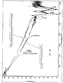
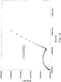
- FIG. 2 illustrates diffusion of the layer 102 and/or the coating 101 into the substrate 100 according to an exemplary embodiment. Applying dimethylsilane to preselected surfaces has resulted in improved chemical resistance, improved inertness, and improved adhesion over non-diffusion coatings.
- FIG. 2 corresponds to the layer 102 having the first portion 104 with carbon and the second portion 106 having silicon. Specifically, FIG. 2 shows the composition of the layer 102 within the substrate 100 and/or the article 103 by Auger Electron Spectroscopy measurements of the layer 102.
- dimethylsilane is thermally decomposed and deposited as amorphous carbosilane for 15 hours.
- the layer 102 extends to about 130 nanometers and includes a portion of the diffusion region 108 identifiable based upon an increased concentration of O and decreased concentration of C and Si (for example, by at least a factor of four).
- the range of the layer 102 can be between about 0.1 micrometers to about 3.0 micrometers.
- the diffusion region 108 can be between about 5 nanometers and 500 nanometers. In one embodiment, the diffusion region 108 is about 20 nanometers. It will be appreciated that precise measurement of the diffusion layer via Auger Electron Spectroscopy can be offset by surface roughness of the substrate and coating.
- the diffusion region as measured by Auger Electron Spectroscopy is not an absolute measurement but a representation of the diffusion mechanism according to the process.
- the composition of layer 102 is about 1 :0.95:0.12 ratio of C:Si:0.
- the amorphous array provides additional benefits such as decreased cracking or flaking, for example, upon tensile or compressive forces acting on the substrate 100, and/or increased adhesion.
- multiple layers of the coating 101 or similar coatings are deposited for thicker layers or for desired properties.
- FIG. 3 shows an exemplary embodiment having a functionalized layer 110.
- R-groups can be formed by any suitable organic reagent having one or more unsaturated hydrocarbon groups.
- R-groups can be formed by hydrocarbons, substituted hydrocarbons (for example, halogenated), carbonyls, carboxyls, esters, ethers, amines, amides, sulfonic acids, organometallic complexes, and/or epoxides.
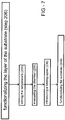
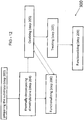
- FIG. 4 shows an exemplary chemical vapor deposition method 200 for forming the layer 102 that includes preparing the substrate (step 202) and thermally decomposing dimethylsilane (step 204).
- Preparing the substrate (step 202) can be performed by any suitable treatment method.
- preparing the substrate (step 202) can include isolating a substrate in a chemical vapor deposition chamber (substep 208), preheating the substrate (substep 210), flushing the chamber (substep 212) with an inert gas, and evacuating the chamber (substep 214).
- Isolating the substrate is performed in an inert atmosphere within the chamber.
- the flow of gas and/or maintenance of a vacuum in the chamber can provide the controlled atmosphere.
- a heat source can control the temperature in the chamber to desorb water and remove remaining contaminants from the substrate surface (substep 210).
- the surface to be treated can be included within a chemical vapor deposition chamber with tubing connections to allow gas flow in and out of the chemical vapor deposition chamber.
- the chamber can include multiple controlled inlets and outlets configured for providing and removing multiple gas streams.
- a vacuum may be connected to one or more outlet tubes.
- the substrate may be prepared by heating (substep 210) at a temperature above about 100°C at a pressure of below about 1 atmosphere for a period ranging from a few minutes to about 15 hours. Generally, the temperature of the heating corresponds to the properties of the substrate 100. In one embodiment, the period is from about 0.5 to about 15 hours. In another embodiment, the substrate is heated at about 450°C for about 2 hours.
- the chamber may be selectively flushed (substep 212) with an inert gas and evacuated (substep 214).
- Method 200 includes thermally decomposing the dimethylsilane (step 204).
- dimethylsilane is not readily obtainable due to the low demand for it.
- Dimethylsilane has been regarded as undesirable in some chemical vapor deposition applications because it includes carbon and is much more expensive than silane.
- Silane and the monomethyl analogue to dimethylsilane, methylsilane are both pyrophoric and may explode in air.
- Dimethylsilane although flammable, is not pyrophoric.
- use of dimethylsilane can decrease safety risks.
- use of dimethylsilane can result in inertness of a coating and/or chemical resistance, thereby protecting a surface of a substrate.
- thermal decomposition of dimethylsilane includes introducing dimethylsilane (substep 216) into the chamber at a predetermined pressure and temperature sufficient to decompose dimethylsilane, depositing constituents from decomposition onto the substrate 100 (substep 217), coating the substrate (substep 218) for a predetermined period of time to achieve a predetermined thickness, and/or purging the chamber of dimethylsilane (substep 220).
- exemplary process conditions may include pressure being between about 0.01 psia to about 200 psia.
- the temperature can be between about 200° and 600°C.
- the time period can be from about 10 minutes to about 24 hours.
- the dimethylsilane introduced (substep 216) includes dimethylsilane in gaseous form.
- the substrate is exposed to dimethylsilane gas at a pressure between about 1.0 psia and about 100 psia and a temperature between about 300° and 600°C for a time of about 30 minutes to about 24 hours.
- the substrate 100 is exposed to dimethylsilane gas at a temperature between about 400° and about 500°C for about 15 hours.
- the dimethylsilane is then thermally dissociated into molecular fragments including H, C, Si, and combinations thereof, and the constituents are deposited onto the substrate 100 (substep 217), thereby forming the coating 100 (substep 218) with a material including silicon, carbon, and hydrogen resulting from decomposition of dimethylsilane.
- Dimethylsilane gas may be introduced into the reaction chamber under reduced pressure or with an inert gas, such as nitrogen, helium, and/or argon, as a partial pressure dilutant.
- the resultant coating includes amorphous carbosilanes having carbon, silicon, and hydrogen on the substrate surface as well as on exposed surfaces of the chamber.
- the deposited material also diffuses into the surface 105 of the substrate 100 as is illustrated in the Auger Electron Spectroscopy depth profile ( FIG. 2 , the diffusion region 108) thus supporting the mode of adhesion to the substrate 100.
- the chamber may then be purged of dimethylsilane and volatile, non-deposited carbosilyl fragments (substep 220). If a thicker deposition layer is desired, deposition conditions are changed. This is accomplished by changing temperature, pressure, time, or combinations thereof. Multiple layers can also be applied by repeating step 204.
- the layer 102 is functionalized next (step 206) as further described below with reference to FIG. 7 to form the functionalized layer 1 10.
- the layer 102 for example, amorphous carbosilane
- the layer 102 is oxidized (step 205) as further described below with reference to FIG. 8 to form an initially-oxidized layer 802 (for example, amorphous carboxysilane).
- the functionalized layer 1 10 (for example, functionalized amorphous carbosilane) is oxidized with water to form a functionalized-then-oxidized layer 804 (for example, functionalized amorphous carboxysilane) as further described below with reference to FIG. 9 .
- the oxidized layer 802 is functionalized to form an oxidized-then-functionalized layer (not shown).
- the term "oxidized layer” generally refers to one or more of the initially-oxidized layer 802, the functionalized-then-oxidized layer 804, and the oxidized-then-functionalized layer (not shown).
- the method 200 further includes functionalizing the layer 102 of the substrate 100 (step 206) to form the functionalized layer 1 10, as briefly discussed above with reference to FIG. 3 .
- functionalizing the layer 102 of the substrate 100 (step 206) may be performed by reacting with silicon hydride moieties remaining from the original carbosilane deposition (step 204).
- the system is purged with an inert gas (which can be purging of substep 220 or a separate purge step) while the reaction chamber can be set to a predetermined functionalization temperature (substep 232).
- the purge removes gaseous carbosilane moieties and/or unreacted dimethlysilane moieties not bound to the substrate surface.
- the chamber is evacuated (substep 234).
- a binding agent is introduced into the chamber at a predetermined temperature and pressure within the chamber (substep 236).
- the binding reagent reacts with and binds to the carbosilyl surface via silicon hydride moieties.
- R-groups can be formed by hydrocarbons, substituted hydrocarbons (for example, halogenated), carbonyls, carboxyls, esters, ethers, amines, amides, sulfonic acids, organometalic complexes, and/or epoxides.
- binding agent molecules are then bound to the substrate (substep 240).
- the coating can include a carbon-silicon covalent bond with an R-group.
- the R-group can be modified to adjust the properties of the surface.
- the R-group can be modified to adjust the hydrophobicity of the surface.
- the R-group can be a fluorinated hydrocarbon.
- the fluorinated hydrocarbon can form a hydrophobic and/or oleophobic surface.
- the R-group can include an organometallic substituent providing catalytic or biocidal properties.
- the moieties of silicon hydride can thermally react, via a hydrosilyation mechanism, with unsaturated hydrocarbon groups to covalently bond to the surface of the coated substrate.
- the resultant coating on all exposed surface within the reaction chamber includes covalently-bound R-groups which includes the R-group and carbon, silicon, and hydrogen moieties.
- method 200 further includes oxidizing the layer 102 of the substrate 100 (step 205) as briefly described above.
- Layer 102 is oxidized to form the oxidized layer (see above) by exposure to any suitable chemical species capable of donating a reactive oxygen species into the layer 102 under predetermined oxidation conditions.
- the chemical species may be water, oxygen, air, nitrous oxide, ozone, peroxide, and combinations thereof.
- oxidation is a bulk reaction that affects the bulk of the coating 101. The oxidation may be controlled by increasing or decreasing the temperature within the chamber, the exposure time within the chamber, the type and/or amount of diluent gases, pressure, and/or other suitable process conditions.
- Control of the oxidation can increase or decrease the amount and/or depth of oxidation and, thus, the wear resistance and/or hardness of the surface.
- the layer 102 is exposed to water (for example, in an inert gas at a pressure of about 100 to 200 psia for about 450°C for about two hours).
- the functionalized layer 1 10 is exposed to water (for example, in an inert gas at a pressure of about 100 to 200 psia for about 450°C for about two hours).
- the layer 102 is an amorphous layer of carbosilane that is oxidized to form an amorphous layer of carboxysilane as the initially- oxidized layer 802.
- the functionalized layer 110 is an amorphous layer of functionalized carbosilane that is oxidized to form an amorphous surface of functionalized carboxysilane as the functionalized-then-oxidized layer 804.
- the oxidizing (step 205) is performed with nitrous oxide (N 2 0). Specifically, N 2 0 is applied under heat (for example, about 450°C) with a pressure of pure N 2 0 in a vessel with carbosilane-coated samples.
- the oxidizing (step 205) over-oxidizes and the over-oxidizing results in having a contact angle of about 60°, increases an amount of N-H, Si-OH, and/or C-OH groups, results in having relatively fragile scratch resistance, and increases acid resistance / corrosion resistance.
- the oxidizing (step 205) is performed with ozone.
- the oxidizing (step 205) decreases wear resistance, decreases chemical resistance, decreases scratch resistance, decreases hardness, and increases acid resistance / corrosion resistance.
- the oxidizing (step 205) is performed with water (only) as an oxidizing reagent (for example, at a temperature of about 450°C).
- the oxidizing (step 205) results in having a contact angle on a Si wafer of about 86.6°, lowers friction (in comparison to using an oxidizing reagent of air and water), decreases wear resistance (for example, in comparison to using an oxidizing reagent of air and water), and forms Si-O-Si groups (as illustrated in FIG. 10 by a growth of the Si-O-Si peak at 1026.9 cm -1 compared to the non-water functionalized peak at 995.2 cm -1 ).
- the oxidizing (step 205) is performed with an oxidizing reagent including air and water (for example, at a temperature of about 450°C).
- oxidizing (step 205) over-oxidizes and decreases an amount of C-H groups (for example, in comparison to using water alone as an oxidizing reagent), decreases an amount of Si-C groups (for example, in comparison to using water alone as an oxidizing reagent), and increases an amount of Si-OH/C-OH groups (for example, in comparison to using water alone as an oxidizing reagent).
- the oxidizing (step 205) is performed with air (only) (for example, at a temperature of about 450°C).
- air only
- oxidizing (step 205) lowers friction (for example, in comparison to using an oxidizing reagent of air and water), increases wear resistance (for example, in comparison to using an oxidizing reagent of air and water), and forms Si-O-Si groups.
- the layer 102 has a predetermined contact angle (for example, about 98.3° advancing) and the functionalized layer 1 10 has a higher contact angle (for example, about 100° advancing). In one embodiment, the layer 102 has a predetermined contact angle (for example, about 95.6° advancing) and a functionalized then oxidized layer 804 has a lower contact angle (for example, about 65.9° receding). In this embodiment, the oxidizing (step 205) forms Si-O-Si groups and decreases an amount of Si-H groups (for example, in comparison to the functionalized layer 1 10).
- the oxidized layer has a lower coefficient of friction (for example, about 0.84) than the non-oxidized layer 102 (for example, about 0.97). Similarly, in one embodiment, the oxidized layer has a lower wear rate (for example, about 6.75 x 10 -5 mm 3 /Nm) than the non-oxidized layer 102 (for example, 4.73 x 10 -4 mm 3 /Nm).
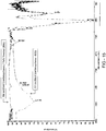
- FIG. 1 1 illustrates diffusion of the oxidized layer into the substrate 100 (for example, stainless steel) according to an exemplary embodiment using water for oxidation.
- FIG. 11 shows the composition of the oxidized layer within the substrate 100, the coating 101, and the article 103 by Auger Electron Spectroscopy.
- the oxidation is illustrated by Si-H moieties undergoing oxidation and elimination to create Si-O-Si linkages, as well as some Si-C and/or free carbon species being eliminated.
- the oxidized layer extends to about 1600 Angstroms and includes the diffusion region 108 being about 250 Angstroms, identifiable based upon a decreased concentration of C and Si.
- the range of the oxidized layer can be between about 0.1 micrometers and about 3.0 micrometers.
- the diffusion region 108 can be between about 5 nanometers and 500 nanometers.
- the composition of the oxidized layer is about 1.0: 1.22:0.91 (C:Si:0) with an increase in oxygen due to the preexisting oxide layer on substrate 100.
- the layer 102 can also be oxidized in the presence of a different oxidation reagent.
- the oxidation reagent is zero air.
- zero air refers to atmospheric air having less than about 0.1 ppm total hydrocarbons.
- the oxidation reagent consists of gaseous reagents. Due to the gaseous processing agents (for example, dimethylsilane and/or nitrogen) being in the gas phase, use of a gaseous oxidation reagent results in simpler scale-up for manufacturing, a more transferable process, and a more economical process.
- the oxidizing agents herein may be satisfactory in many instances, in some cases using water as the oxidation reagent presents various complexities. To achieve pressure and corrosion-resistance specifications, the size and weight of the chambers necessary can be very high and pose safety hazards. To safely inject water into the chamber, substantial cooling is used. For example, for a chamber that runs at greater than about 300°C, the system is first cooled below about 100°C. This can result in a drain on energy and/or time of manufacturing resources. Also, accurate dispensing of the water into the chamber can be complicated and expensive due to the water being a liquid.
- the coated material formed may include the presence of - OH functionalities that can lead to adsorption in analytical and chromatographic applications.
- the material formed can have low impedance values at low frequency translating to inferior anti-corrosive performance. Also, the material formed can have low water contact angle values or high hydrophilicity.
- the coating 101 includes the presence of -OH functionalities that lead to adsorption in analytical and chromatographic applications.
- the coating 101 has low impedance values at low frequency translating to inferior anti-corrosive performance.
- the coating 101 has low contact angle values or high hydrophilicity.
- the method 300 includes treating (for example, heating and/or modifying the surface of) the layer 102 of the substrate 100 (step 207) to form a treated layer 806, further described below with reference to FIG. 13 .
- the method 300 includes the method 200 shown in FIG. 4 and the treating (step 207).
- the treating (step 207) follows the oxidizing (step 205), for example, of the initially-oxidized layer 802.
- functionalizing (step 209) follows the treating (step 207).
- the oxidized layer such as an air-oxidized layer 805 is treated (step 207) to form the treated layer 806 (for example, a trimethylsilyl treated amorphous carboxysilane layer) as illustrated in FIG. 13 .
- the treated layer 806 for example, a trimethylsilyl treated amorphous carboxysilane layer
- the treated layer 806 can have greater wear resistance than the functionalized layer 1 10 formed with dimethylsilane and/or the air- oxidized layer 805.
- the treating (step 207) increases wear resistance.
- the treated layer 806 has about a thirty-four- fold improvement in wear resistance over the functionalized layer 1 10 formed with dimethylsilane.
- Forming the treated layer 806 may be performed by reacting (for example, with -OH (hydroxyl) groups on silicon (silanols)) to undergo a condensation reaction (for example, with Si-H (silane) groups).
- the adjustments increase or decrease hardness and wear resistance, inertness, electrochemical impedance, contact angle, and combinations thereof, thereby providing physical performance characteristics expanding the applicability and durability for use in the fields of process, analytical, gas, oil and semiconductor industries.
- the R-groups can be formed by hydrocarbons, substituted hydrocarbons, carbonyls, carboxyls, esters, ethers, amines, amides, sulfonic acids, organometalic complexes, and/or epoxides.
- the moieties of silicon hydride can thermally react, via a hydrosilyation mechanism, with unsaturated hydrocarbon groups to covalently bond to the surface of the coated substrate.
- the coating 101 on all exposed surface within the reaction chamber includes covalently-bound R-groups which include the R-group and carbon, silicon, and hydrogen moieties.
- FIG. 14 illustrates diffusion of the treated layer 806 into the substrate 100 (for example, stainless steel) according to an exemplary embodiment.
- FIG. 14 shows the composition of the treated layer 806 within the substrate 100 and/or article 103 by Auger Electron Spectroscopy.
- the treatment results in a substantially stable concentration of Si, O, and C throughout the treated layer 806 until reaching the diffusion layer 108.
- Si, O, and C atomic concentrations are at about 40%, 35%, and 20%, respectively.
- the treated layer 806 extends to about 3500 Angstroms and includes the diffusion region 108 being about 400 Angstroms, identifiable based upon a decreased concentration of C and Si and a spike and then decrease in O.
- the range of the treated layer 806 can be between about 0.1 micrometers and about 3.0 micrometers.
- the diffusion region 108 can be between about 5 nanometers and 500 nanometers.
- the composition of the treated layer 806 is about 1.0:2.25:1.75 (C:Si:0).
- the treating (step 207) includes exposure of the article 100, the coating 101 , the layer 102, the functionahzed layer 1 10, the air-oxidized layer 805, or combinations thereof to an organosilane reagent.
- the organosilane reagent is a trifunctional organosilane that consists of the general formula RR'R"Si-H, where R,R',R" are organo functional groups. Examples of the organofunctional groups are alkyl, aryl, halogenated alkyl and aryl, ketones, aldehydes, acyl, alcohol, epoxy, and nitro -organo groups, and organometallic functionalities.
- the organosilane is trimethylsilane.
- the air-oxidized layer 805 (for example, a dimethylsilane-based carboxysilane layer formed by air-oxidizing the layer 102) is treated by exposure to trimethylsilane (for example, at 450° C for 10 hours at 25 psia).
- the treated layer 806 includes a loss of Si-OH functionality (in comparison to the air-oxidized layer 805, see FIG.
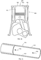
- FIGS. 20 and 21 illustrates an application in which two surfaces 901 and 902 are in contact and are moved relative to each other in a reciprocating motion.
- the surfaces are on a piston head 903 and a cylinder 904, but the surfaces could be on any moving parts.
- FIG. 21 illustrates an application is which a surface 910 contacted by a moving fluid.
- the surface is the interior of a pipe 911 through which a fluid such as gas and/or liquid flow(s), as indicated by arrows 912, but the surface could be on any part which is in contact with fluid motion.
- the coating 101 and/or the layer 102 be formulated to prevent both the chemical and physical degradation to the surface of the component.
- An example of an application of a component working in an aggressive environment is a drilling tool used in the oil and gas industry. The tool experiences high loads, high speeds and friction and, as a consequence high temperatures. These factors can lead to surface wear of the components.
- Other such applications in aggressive or harsh environments in which the coating 101 and/or the layer 102 may be of benefit include, but are not limited to, systems or components with particulate flow and/or sliding wear.
- Such applications include, but are not limited to, tubing, fittings, valves (rotary, ball, slide, etc.), injectors, piston rings, sliding o-rings, cylinders, regulators, mixing systems, sampling apparatus, analytical systems for use in the oil and gas industry, process and analytical equipment, internal combustions engines, semiconductors, and the like.
- the coating 101 or the layer 102 has a thickness of about 100 nm to about 10,000 nm or, more specifically, about 200 nm to about 5,000 nm, or, even more specifically, about 300 nm to about 1500 nm.
- the wear resistance ranges between about 13 x 10 mm 3 /Nm and about 0.5 x 10 -5 mm 3 /Nm, or more specifically, between about 9 x 10 -5 mm 3 /Nm and about 1 x 10 -5 mm 3 /Nm, or, even more specifically, between about 6.2 x 10 -5 mm 3 /Nm and about 1.3 x 10 -5 mm 3 /Nm.
- the coefficient of friction ranges between about 0.58 and about 0.05 or, more specifically, between about 0.5 and about 0.075, or, even more specifically, between about 0.38 and about 0.1.
- the coatings 101 and/or the layers 102 applied in accordance herewith improve resistance to the wear caused by stress interactions and deformation properties of the mating surfaces, such as abrasion, adhesion and fatigue.
- Abrasive wear also referred to as scratching, gouging or scoring
- Adhesive wear (often called galling or scuffing) occurs where interfacial adhesive junctions lock together as two surfaces slide across each other under pressure. As normal pressure is applied, local pressure at the asperities become extremely high, often exceeding the yield stress causing the asperities to deform plastically. Fatigue occurs when the periodic motion of mechanical machinery cause stresses to the surfaces of the component.
- the coating 101 and/or layer 102 improve the resistance of the surface of the component to erosion (from both solid and liquid) and corrosion. Erosion (from both solid and liquid) occurs when an impinging particle or stream contacts the surface of the component. In corrosive wear the connecting surfaces react with the environment and reaction products are formed on the surface asperities. Attrition of the reaction products then occurs as a result of crack formation, and/or abrasion, in the contact interactions of the materials.
- the coating 101 and/or the layer 102 made and applied in accordance herewith provides increased adhesion of the coating 101 and/or the layer 102 to the substrate 100, thereby improving the wear characteristics of the coating 102 and/or the layer 102.
- the coating 101 and/or the layer 102 is hard and adheres tenaciously to a bearing surface of the substrate 100. This allows the coating 101 and/or the layer 102 to be used in aggressive or harsh environments in which the substrate 100 is exposed is subject to wear and/or erosion.
- either surface 901, 902 may have the coating 101 applied thereto.
- both surfaces 901, 902 may have the coating applied.
- the surface 910 may have the coating 101 applied.
- an outer surface 913 may have the coating 101 applied to protect the item 91 1 from damage during transportation and the like.
- the first example included introducing dimethylsilane to the substrate 100 for 2 hours at 8 psia* gas at 450°C to form the layer 102.
- the layer 102 was almost undetectable (i.e., very difficult to visually discern) on a mirror-polished 316 stainless steel coupon (slightly yellowed). Measurements showed water contact angle data prior to the deposition treatment at around 60°. After the deposition treatment with dimethylsilane, the contact angle increased to around 102°. Although the layer 102 was not visible, the data indicated an extremely thin deposition with a significant density of carbosilyl material on the layer 102 of the surface 105. The thickness of the layer 102 was estimated to be at about 100 Angstroms as available spectroscopic techniques were not sensitive enough to detect the coating.
- the second example included introducing dimethylsilane to the substrate 100 for 15 hours at 8 psia* gas at 450°C to form the layer 102.
- the layer 102 had a visible luminescent rainbow array of colors. Measurements showed average deionized water contact angle data around 100°, for mirror-finished 316 stainless steel surfaces and polished silicon wafer surfaces. FT-IR indicated the presence of C-H based upon a reading at 2950 cm -1 , the presence of Si-C based upon a reading at 792 cm -1 , and the presence of Si-H moieties based upon a reading at 2102 cm -1 . The thickness of the layer 102 was determined by spectrometer to be about 800 Angstroms.
- the third example included introducing dimethylsilane to the substrate 100 for 15 hours at 8 psia* gas at 450°C to form the layer 102 and subsequently oxidizing the layer 102 of the substrate 100 with water in an inert gas for 2 hours at about 100 to 200 psia* gas at 450°C to form the oxidized layer 802.
- the third example showed undesirable results. For example, FT-IR data failed to reveal the presence of any functional moieties (Si-OH or Si-H) for surface modification chemistry.
- the oxidized layer 802 had a contact angle on a Si wafer of 86.6°, and a presence of Si-O-Si groups.
- the fourth example included introducing dimethylsilane to the substrate 100 for 15 hours at 8 psia* gas at 450°C to form the layer 102 and subsequently oxidizing the layer 102 of the substrate 100 with an oxidation reagent mixture for 2 hours at about 100 to 200 psia* gas at 300°C to form the oxidized layer 805.
- the oxidation reagent mixture included air and water.
- the fourth example showed undesirable results. According to FT-IR data, the oxidized layer 805 was over-oxidized, had a decrease of C-H groups (in comparison to Example 3), a decrease of Si-C groups (in comparison to Example 3), and an increase of Si-OH/C-OH groups (in comparison to Example 3).
- the fifth example included introducing dimethylsilane to the substrate 100 for 15 hours at 8 psia* gas at 450°C to form the layer 102 and subsequently oxidizing the layer 102 on the substrate 100 with air for 2 hours at about 100 to 200 psia* gas at 300 °C to form the oxidized layer 805.
- Wear resistance of the material was analyzed with a Tribometer (CSM Instruments S/N 18-343) applying a 0.5 N force via a standard 100 Cr6 ball and circular linear speed of 3.00 cm/s thereby showing a 4.141 x 10 -3 wear (mm 3 /N-m).
- the oxidized layer 805 had lower friction (in comparison to Example 3), higher wear (in comparison to Example 3), and a presence of Si-O-Si groups.
- the sixth example included functionalizing the layer 102 formed in Example 2 with ethylene to form the functionalized layer 1 10.
- the functionalized layer 1 10 had a water contact angle of 98.3° advancing and 85.1 ° receding.
- FT-IR data showed little oxidation occurred based upon a lack of Si-O-Si groups (based upon a stretch at 1027 cm -1 ) and decreased an amount of Si-H groups (based upon a stretch at 2091 cm -1 ).
- the seventh example including functionalizing the layer 102 formed in Example 2 with ethylene to form the functionalized layer 1 10.
- the functionalized layer 110 was oxidized by 5ml deionized water (DI) being added to the chamber.
- DI deionized water
- the chamber was exposed to several nitrogen flushes and mild vacuum to remove air from the sealed container.
- the temperature in the chamber was held at 450°C for about 2 hours, then returned to room temperature.
- the oxidation of the functionalized layer 110 formed the functionalized then oxidized layer 804.
- the functionalized then oxidized layer 804 had a water contact angle data of 95.6° advancing and 65.9° receding. As shown in FIG.
- FT-IR showed that oxidation increased an amount of Si-O-Si groups (based upon a stretch at 1027 cm -1 ) and decreased an amount of Si-H groups (based upon a stretch at 2091 cm -1 ) in comparison to the functionalized layer 110 formed in Example 6.
- the eighth example included introducing trimethylsilane to the layer 102 (dimethylsilane) for 15 hours at 8 psia* gas at 450°C.
- the eighth example showed undesirable results, including no visible or spectroscopically measurable coating on the substrate 100, nor was there any indication of a molecular coating as there was no significant change in water contact angle values.
- the ninth example included treating the oxidized layer 805 formed in Example 5 with trimethylsilane to form the treated layer 806.
- trimethylsilane was added to an evacuated chamber including the material at 450°C and 25 psia* and reacted for about 10 hours.
- Resultant FT-IR data showed a loss of Si-OH functionality (see FIG. 15 ).
- Contact angle was measured to be 99.1° for deionized water, suggesting a presence of hydrophobicity.
- Electrochemical impedance spectroscopy showed impedance at low frequency (Zi f ) of 15.4 Mohm.
- Electrochemical impedance spectroscopy also showed a Bode plot and terminal ZR/ZI ratio of 0.072 from a Nyquist plot (see FIGS.
- Wear resistance of the material was analyzed with a Tribometer (CSM Instruments S/N 18-343) applying a 0.5 N force via a standard 100 Cr6 ball and circular linear speed of 3.00 cm/s thereby showing a 1.225 x 10 -4 wear (mm 3 /Nm), a thirty-four-fold increase in comparison to the non-treated material.
Claims (8)
- Artikel, der eine Verschleißbeschichtung aufweist, umfassend eine Schicht, die durch Trimethylsilan behandelt ist, die auf mindestens eine Oberfläche des Artikels aufgebracht wird, wobei die Verschleißbeschichtung durch chemische Gasphasenabscheidung über thermische Zersetzung von Dimethylsilan aufgebracht wird, und wobei Bestandteile des zersetzten Dimethylsilans vor der Trimethylsilanbehandlung oxidiert werden.
- Artikel nach Anspruch 1, wobei Bestandteile des zersetzten Dimethylsilans funktionalisiert sind.
- Artikel nach Anspruch 1, wobei die Verschleißbeschichtung eine Dicke von 100 nm bis 10.000 nm aufweist.
- Artikel nach Anspruch 1, wobei die Verschleißbeschichtung einen Verschleißwiderstand zwischen 13 x 10-5 mm3/Nm und 0,5 x 10⁻⁵ mm3/Nm aufweist.
- Artikel nach Anspruch 1, wobei die Verschleißbeschichtung einen Reibungskoeffizienten zwischen 0,58 und 0,05 aufweist.
- Artikel nach Anspruch 1, wobei die Verschleißbeschichtung auf eine sich bewegende Oberfläche des Artikels oder auf eine feststehende Oberfläche des Artikels aufgebracht wird.
- Artikel nach Anspruch 1, wobei die Oberfläche des Artikels, auf welche die Verschleißbeschichtung aufgebracht wird, aus einem Material hergestellt ist, das aus der Gruppe ausgewählt ist, die aus Metall, Keramik, Glas und Kombinationen davon besteht.
- Artikel nach Anspruch 1, wobei die Verschleißbeschichtung eine Dicke im Bereich von 100 nm bis 10.000 nm, einen Verschleißwiderstand im Bereich von 13 x 10-5 mm3/Nm bis 0,5 x 10⁻⁵ mm3/Nm und einen Reibungskoeffizienten zwischen 0,58 und 0,05 aufweist.
Applications Claiming Priority (3)
| Application Number | Priority Date | Filing Date | Title |
|---|---|---|---|
| US38977710P | 2010-10-05 | 2010-10-05 | |
| US201161507650P | 2011-07-14 | 2011-07-14 | |
| PCT/US2011/054835 WO2012047945A2 (en) | 2010-10-05 | 2011-10-05 | Wear resistant coating, article, and method |
Publications (2)
| Publication Number | Publication Date |
|---|---|
| EP2625307A2 EP2625307A2 (de) | 2013-08-14 |
| EP2625307B1 true EP2625307B1 (de) | 2017-11-15 |
Family
ID=44936522
Family Applications (1)
| Application Number | Title | Priority Date | Filing Date |
|---|---|---|---|
| EP11773611.6A Active EP2625307B1 (de) | 2010-10-05 | 2011-10-05 | Verschleissresistente artikel |
Country Status (6)
| Country | Link |
|---|---|
| US (3) | US10604660B2 (de) |
| EP (1) | EP2625307B1 (de) |
| JP (1) | JP5710770B2 (de) |
| KR (3) | KR101512579B1 (de) |
| CN (1) | CN103237920B (de) |
| WO (1) | WO2012047945A2 (de) |
Families Citing this family (28)
| Publication number | Priority date | Publication date | Assignee | Title |
|---|---|---|---|---|
| KR101932899B1 (ko) | 2009-10-27 | 2018-12-26 | 실코텍 코포레이션 | 화학적 증기 증착 코팅, 물품, 및 방법 |
| US9340880B2 (en) | 2009-10-27 | 2016-05-17 | Silcotek Corp. | Semiconductor fabrication process |
| KR101512579B1 (ko) * | 2010-10-05 | 2015-04-15 | 실코텍 코포레이션 | 내마모성 코팅, 물건 및 방법 |
| US9975143B2 (en) | 2013-05-14 | 2018-05-22 | Silcotek Corp. | Chemical vapor deposition functionalization |
| US20150030885A1 (en) * | 2013-07-29 | 2015-01-29 | Silcotek Corp. | Coated article and chemical vapor deposition process |
| US11292924B2 (en) * | 2014-04-08 | 2022-04-05 | Silcotek Corp. | Thermal chemical vapor deposition coated article and process |
| SG10201506024WA (en) * | 2014-08-21 | 2016-03-30 | Silcotek Corp | Semiconductor fabrication process |
| SG10201506694QA (en) * | 2014-09-03 | 2016-04-28 | Silcotek Corp | Chemical vapor deposition process and coated article |
| US9915001B2 (en) | 2014-09-03 | 2018-03-13 | Silcotek Corp. | Chemical vapor deposition process and coated article |
| US10316408B2 (en) * | 2014-12-12 | 2019-06-11 | Silcotek Corp. | Delivery device, manufacturing system and process of manufacturing |
| US20160289824A1 (en) * | 2015-04-01 | 2016-10-06 | Silcotek Corp. | Article including a coating and process including an article with a coating |
| US20160289124A1 (en) * | 2015-04-01 | 2016-10-06 | Silcotek Corp. | Thermal chemical vapor deposition product and process of using a thermal chemical vapor deposition product |
| US20160289585A1 (en) * | 2015-04-01 | 2016-10-06 | Silcotek Corp. | Thermal chemical vapor deposition coated product and process of using a thermal vapor deposition coated product |
| WO2017040623A1 (en) | 2015-09-01 | 2017-03-09 | Silcotek Corp. | Thermal chemical vapor deposition coating |
| US10029346B2 (en) * | 2015-10-16 | 2018-07-24 | Applied Materials, Inc. | External clamp ring for a chemical mechanical polishing carrier head |
| US10578050B2 (en) | 2015-11-20 | 2020-03-03 | Tenneco Inc. | Thermally insulated steel piston crown and method of making using a ceramic coating |
| US10519854B2 (en) | 2015-11-20 | 2019-12-31 | Tenneco Inc. | Thermally insulated engine components and method of making using a ceramic coating |
| GB201520964D0 (en) * | 2015-11-27 | 2016-01-13 | Porvair Filtration Group Ltd | Filtration material and method of manufacture thereof |
| US10323321B1 (en) | 2016-01-08 | 2019-06-18 | Silcotek Corp. | Thermal chemical vapor deposition process and coated article |
| US10487403B2 (en) * | 2016-12-13 | 2019-11-26 | Silcotek Corp | Fluoro-containing thermal chemical vapor deposition process and article |
| US11161324B2 (en) * | 2017-09-13 | 2021-11-02 | Silcotek Corp. | Corrosion-resistant coated article and thermal chemical vapor deposition coating process |
| US11709155B2 (en) | 2017-09-18 | 2023-07-25 | Waters Technologies Corporation | Use of vapor deposition coated flow paths for improved chromatography of metal interacting analytes |
| US11709156B2 (en) | 2017-09-18 | 2023-07-25 | Waters Technologies Corporation | Use of vapor deposition coated flow paths for improved analytical analysis |
| CN113272469B (zh) * | 2018-11-29 | 2023-12-05 | 西尔科特克公司 | 流体接触方法、经涂覆的制品以及涂覆方法 |
| WO2020252306A1 (en) | 2019-06-14 | 2020-12-17 | Silcotek Corp. | Nano-wire growth |
| US11918936B2 (en) | 2020-01-17 | 2024-03-05 | Waters Technologies Corporation | Performance and dynamic range for oligonucleotide bioanalysis through reduction of non specific binding |
| EP4189018A1 (de) | 2020-07-30 | 2023-06-07 | Silcotek Corp. | Wärmetauscherverfahren |
| WO2023081013A1 (en) * | 2021-11-03 | 2023-05-11 | Silcotek Corp. | Process, component, and system with amorphous silicon-containing coating exposed to a temperature of greater than 600 degrees celsius |
Family Cites Families (48)
| Publication number | Priority date | Publication date | Assignee | Title |
|---|---|---|---|---|
| FR2371524A1 (fr) | 1976-11-18 | 1978-06-16 | Alsthom Atlantique | Procede de depot d'une couche mince par decomposition d'un gaz dans un plasma |
| US4579752A (en) | 1984-10-29 | 1986-04-01 | At&T Bell Laboratories | Enhanced corrosion resistance of metal surfaces |
| US4671997A (en) | 1985-04-08 | 1987-06-09 | United Technologies Corporation | Gas turbine composite parts |
| US4714632A (en) | 1985-12-11 | 1987-12-22 | Air Products And Chemicals, Inc. | Method of producing silicon diffusion coatings on metal articles |
| US4792460A (en) | 1986-07-15 | 1988-12-20 | Electric Power Research Institute, Inc. | Method for production of polysilanes and polygermanes, and deposition of hydrogenated amorphous silicon, alloys thereof, or hydrogenated amorphous germanium |
| US4741964A (en) | 1986-07-17 | 1988-05-03 | International Business Machines Corporation | Structure containing hydrogenated amorphous silicon and process |
| US4749631B1 (en) | 1986-12-04 | 1993-03-23 | Multilayer ceramics from silicate esters | |
| US4753856A (en) | 1987-01-02 | 1988-06-28 | Dow Corning Corporation | Multilayer ceramic coatings from silicate esters and metal oxides |
| JPH01206629A (ja) * | 1988-02-15 | 1989-08-18 | Toshiba Corp | 薄膜の形成方法 |
| US4842888A (en) | 1988-04-07 | 1989-06-27 | Dow Corning Corporation | Ceramic coatings from the pyrolysis in ammonia of mixtures of silicate esters and other metal oxide precursors |
| US5160544A (en) | 1990-03-20 | 1992-11-03 | Diamonex Incorporated | Hot filament chemical vapor deposition reactor |
| US5270082A (en) | 1991-04-15 | 1993-12-14 | Lin Tyau Jeen | Organic vapor deposition process for corrosion protection of metal substrates |
| FR2675947A1 (fr) | 1991-04-23 | 1992-10-30 | France Telecom | Procede de passivation locale d'un substrat par une couche de carbone amorphe hydrogene et procede de fabrication de transistors en couches minces sur ce substrat passive. |
| TW203633B (de) | 1991-06-03 | 1993-04-11 | L Air Liquide Sa Pour L Expl Des Proce | |
| CA2104340A1 (en) | 1992-08-31 | 1994-03-01 | Grish Chandra | Hermetic protection for integrated circuits |
| US5825078A (en) | 1992-09-23 | 1998-10-20 | Dow Corning Corporation | Hermetic protection for integrated circuits |
| US5249554A (en) * | 1993-01-08 | 1993-10-05 | Ford Motor Company | Powertrain component with adherent film having a graded composition |
| US5299731A (en) | 1993-02-22 | 1994-04-05 | L'air Liquide | Corrosion resistant welding of stainless steel |
| TW347149U (en) | 1993-02-26 | 1998-12-01 | Dow Corning | Integrated circuits protected from the environment by ceramic and barrier metal layers |
| US5465680A (en) * | 1993-07-01 | 1995-11-14 | Dow Corning Corporation | Method of forming crystalline silicon carbide coatings |
| DE69408405T2 (de) | 1993-11-11 | 1998-08-20 | Nissin Electric Co Ltd | Plasma-CVD-Verfahren und Vorrichtung |
| US5818071A (en) | 1995-02-02 | 1998-10-06 | Dow Corning Corporation | Silicon carbide metal diffusion barrier layer |
| US6511760B1 (en) | 1998-02-27 | 2003-01-28 | Restek Corporation | Method of passivating a gas vessel or component of a gas transfer system using a silicon overlay coating |
| US6159871A (en) * | 1998-05-29 | 2000-12-12 | Dow Corning Corporation | Method for producing hydrogenated silicon oxycarbide films having low dielectric constant |
| US6444326B1 (en) * | 1999-03-05 | 2002-09-03 | Restek Corporation | Surface modification of solid supports through the thermal decomposition and functionalization of silanes |
| US6406793B1 (en) * | 1999-09-22 | 2002-06-18 | Shin-Etsu Chemical Co., Ltd. | Addition-reaction silicone pressure sensitive adhesive composition |
| US6472076B1 (en) | 1999-10-18 | 2002-10-29 | Honeywell International Inc. | Deposition of organosilsesquioxane films |
| FR2805583B1 (fr) * | 2000-02-28 | 2002-05-17 | Renault | Piece de friction metallique comportant une couche a proprietes de frottement et d'usure ameliorees |
| US6531398B1 (en) | 2000-10-30 | 2003-03-11 | Applied Materials, Inc. | Method of depositing organosillicate layers |
| US6936309B2 (en) * | 2002-04-02 | 2005-08-30 | Applied Materials, Inc. | Hardness improvement of silicon carboxy films |
| EP1504138A2 (de) * | 2002-05-08 | 2005-02-09 | Applied Materials, Inc. | Verfahren zur härtung von filmen niedriger dielektrizitätskonstante mit einem elektronenstrahl |
| JP4148759B2 (ja) * | 2002-11-13 | 2008-09-10 | 三井化学株式会社 | ガスバリアフィルムの製造方法 |
| US7070833B2 (en) | 2003-03-05 | 2006-07-04 | Restek Corporation | Method for chemical vapor deposition of silicon on to substrates for use in corrosive and vacuum environments |
| JP4300876B2 (ja) * | 2003-05-28 | 2009-07-22 | 株式会社Ihi | 摺動部材及びその製造方法 |
| US20050271893A1 (en) * | 2004-06-04 | 2005-12-08 | Applied Microstructures, Inc. | Controlled vapor deposition of multilayered coatings adhered by an oxide layer |
| US7867627B2 (en) | 2004-12-13 | 2011-01-11 | Silcotek Corporation | Process for the modification of substrate surfaces through the deposition of amorphous silicon layers followed by surface functionalization with organic molecules and functionalized structures |
| US7678712B2 (en) | 2005-03-22 | 2010-03-16 | Honeywell International, Inc. | Vapor phase treatment of dielectric materials |
| US7939172B2 (en) * | 2006-05-17 | 2011-05-10 | G & H Technologies, Llc | Wear resistant vapor deposited coating, method of coating deposition and applications therefor |
| SE0701028L (sv) * | 2007-04-27 | 2008-10-28 | Sandvik Intellectual Property | Skär |
| WO2009032488A1 (en) * | 2007-08-28 | 2009-03-12 | International Business Machines Corporation | Improved low k porous sicoh dielectric and integration with post film formation treatment |
| US7964442B2 (en) * | 2007-10-09 | 2011-06-21 | Applied Materials, Inc. | Methods to obtain low k dielectric barrier with superior etch resistivity |
| JP5143769B2 (ja) * | 2008-03-12 | 2013-02-13 | 東京エレクトロン株式会社 | 半導体装置およびその製造方法 |
| CN102171384B (zh) | 2008-05-28 | 2013-12-25 | 乔治洛德方法研究和开发液化空气有限公司 | 碳化硅基抗反射涂层 |
| KR101932899B1 (ko) | 2009-10-27 | 2018-12-26 | 실코텍 코포레이션 | 화학적 증기 증착 코팅, 물품, 및 방법 |
| KR101512579B1 (ko) * | 2010-10-05 | 2015-04-15 | 실코텍 코포레이션 | 내마모성 코팅, 물건 및 방법 |
| KR20140148409A (ko) | 2012-03-26 | 2014-12-31 | 실코텍 코포레이션 | 코팅된 물품 및 화학적 기상증착방법 |
| US20150030885A1 (en) | 2013-07-29 | 2015-01-29 | Silcotek Corp. | Coated article and chemical vapor deposition process |
| US11292924B2 (en) | 2014-04-08 | 2022-04-05 | Silcotek Corp. | Thermal chemical vapor deposition coated article and process |
-
2011
- 2011-10-05 KR KR1020137011766A patent/KR101512579B1/ko active IP Right Grant
- 2011-10-05 WO PCT/US2011/054835 patent/WO2012047945A2/en active Application Filing
- 2011-10-05 KR KR1020177030045A patent/KR101854162B1/ko active IP Right Grant
- 2011-10-05 US US13/876,328 patent/US10604660B2/en active Active
- 2011-10-05 CN CN201180058513.2A patent/CN103237920B/zh active Active
- 2011-10-05 EP EP11773611.6A patent/EP2625307B1/de active Active
- 2011-10-05 KR KR1020147031583A patent/KR101790206B1/ko active IP Right Grant
- 2011-10-05 JP JP2013532892A patent/JP5710770B2/ja active Active
-
2020
- 2020-02-26 US US16/801,230 patent/US11807777B2/en active Active
-
2023
- 2023-06-08 US US18/331,647 patent/US20230383126A1/en active Pending
Non-Patent Citations (1)
| Title |
|---|
| None * |
Also Published As
| Publication number | Publication date |
|---|---|
| WO2012047945A2 (en) | 2012-04-12 |
| KR101512579B1 (ko) | 2015-04-15 |
| EP2625307A2 (de) | 2013-08-14 |
| KR20130064819A (ko) | 2013-06-18 |
| KR20170119745A (ko) | 2017-10-27 |
| JP5710770B2 (ja) | 2015-04-30 |
| CN103237920B (zh) | 2016-01-13 |
| US20130244025A1 (en) | 2013-09-19 |
| US20200190336A1 (en) | 2020-06-18 |
| US11807777B2 (en) | 2023-11-07 |
| KR101790206B1 (ko) | 2017-10-25 |
| CN103237920A (zh) | 2013-08-07 |
| WO2012047945A3 (en) | 2012-05-31 |
| JP2013545889A (ja) | 2013-12-26 |
| KR101854162B1 (ko) | 2018-06-20 |
| US20230383126A1 (en) | 2023-11-30 |
| US10604660B2 (en) | 2020-03-31 |
| KR20140138352A (ko) | 2014-12-03 |
Similar Documents
| Publication | Publication Date | Title |
|---|---|---|
| US11807777B2 (en) | Amorphous coating | |
| US10731247B2 (en) | Coated article | |
| US20140370300A1 (en) | Coated article and chemical vapor deposition process | |
| US20150030885A1 (en) | Coated article and chemical vapor deposition process | |
| US20150064376A1 (en) | Coated automotive article | |
| US9340880B2 (en) | Semiconductor fabrication process | |
| US20160289824A1 (en) | Article including a coating and process including an article with a coating | |
| EP2988327A1 (de) | Halbleiterherstellungsverfahren | |
| US20160289585A1 (en) | Thermal chemical vapor deposition coated product and process of using a thermal vapor deposition coated product | |
| US20160289124A1 (en) | Thermal chemical vapor deposition product and process of using a thermal chemical vapor deposition product |
Legal Events
| Date | Code | Title | Description |
|---|---|---|---|
| PUAI | Public reference made under article 153(3) epc to a published international application that has entered the european phase |
Free format text: ORIGINAL CODE: 0009012 |
|
| 17P | Request for examination filed |
Effective date: 20130423 |
|
| AK | Designated contracting states |
Kind code of ref document: A2 Designated state(s): AL AT BE BG CH CY CZ DE DK EE ES FI FR GB GR HR HU IE IS IT LI LT LU LV MC MK MT NL NO PL PT RO RS SE SI SK SM TR |
|
| DAX | Request for extension of the european patent (deleted) | ||
| 17Q | First examination report despatched |
Effective date: 20160323 |
|
| GRAP | Despatch of communication of intention to grant a patent |
Free format text: ORIGINAL CODE: EPIDOSNIGR1 |
|
| STAA | Information on the status of an ep patent application or granted ep patent |
Free format text: STATUS: GRANT OF PATENT IS INTENDED |
|
| INTG | Intention to grant announced |
Effective date: 20170704 |
|
| GRAS | Grant fee paid |
Free format text: ORIGINAL CODE: EPIDOSNIGR3 |
|
| GRAJ | Information related to disapproval of communication of intention to grant by the applicant or resumption of examination proceedings by the epo deleted |
Free format text: ORIGINAL CODE: EPIDOSDIGR1 |
|
| GRAL | Information related to payment of fee for publishing/printing deleted |
Free format text: ORIGINAL CODE: EPIDOSDIGR3 |
|
| STAA | Information on the status of an ep patent application or granted ep patent |
Free format text: STATUS: EXAMINATION IS IN PROGRESS |
|
| GRAR | Information related to intention to grant a patent recorded |
Free format text: ORIGINAL CODE: EPIDOSNIGR71 |
|
| STAA | Information on the status of an ep patent application or granted ep patent |
Free format text: STATUS: GRANT OF PATENT IS INTENDED |
|
| GRAA | (expected) grant |
Free format text: ORIGINAL CODE: 0009210 |
|
| STAA | Information on the status of an ep patent application or granted ep patent |
Free format text: STATUS: THE PATENT HAS BEEN GRANTED |
|
| INTC | Intention to grant announced (deleted) | ||
| INTG | Intention to grant announced |
Effective date: 20171005 |
|
| AK | Designated contracting states |
Kind code of ref document: B1 Designated state(s): AL AT BE BG CH CY CZ DE DK EE ES FI FR GB GR HR HU IE IS IT LI LT LU LV MC MK MT NL NO PL PT RO RS SE SI SK SM TR |
|
| REG | Reference to a national code |
Ref country code: CH Ref legal event code: EP Ref country code: GB Ref legal event code: FG4D Ref country code: AT Ref legal event code: REF Ref document number: 946370 Country of ref document: AT Kind code of ref document: T Effective date: 20171115 |
|
| REG | Reference to a national code |
Ref country code: IE Ref legal event code: FG4D |
|
| REG | Reference to a national code |
Ref country code: DE Ref legal event code: R096 Ref document number: 602011043402 Country of ref document: DE |
|
| REG | Reference to a national code |
Ref country code: NL Ref legal event code: FP Ref country code: CH Ref legal event code: NV Representative=s name: STOLMAR AND PARTNER INTELLECTUAL PROPERTY S.A., CH |
|
| REG | Reference to a national code |
Ref country code: LT Ref legal event code: MG4D |
|
| REG | Reference to a national code |
Ref country code: AT Ref legal event code: MK05 Ref document number: 946370 Country of ref document: AT Kind code of ref document: T Effective date: 20171115 |
|
| PG25 | Lapsed in a contracting state [announced via postgrant information from national office to epo] |
Ref country code: SE Free format text: LAPSE BECAUSE OF FAILURE TO SUBMIT A TRANSLATION OF THE DESCRIPTION OR TO PAY THE FEE WITHIN THE PRESCRIBED TIME-LIMIT Effective date: 20171115 Ref country code: FI Free format text: LAPSE BECAUSE OF FAILURE TO SUBMIT A TRANSLATION OF THE DESCRIPTION OR TO PAY THE FEE WITHIN THE PRESCRIBED TIME-LIMIT Effective date: 20171115 Ref country code: ES Free format text: LAPSE BECAUSE OF FAILURE TO SUBMIT A TRANSLATION OF THE DESCRIPTION OR TO PAY THE FEE WITHIN THE PRESCRIBED TIME-LIMIT Effective date: 20171115 Ref country code: NO Free format text: LAPSE BECAUSE OF FAILURE TO SUBMIT A TRANSLATION OF THE DESCRIPTION OR TO PAY THE FEE WITHIN THE PRESCRIBED TIME-LIMIT Effective date: 20180215 Ref country code: LT Free format text: LAPSE BECAUSE OF FAILURE TO SUBMIT A TRANSLATION OF THE DESCRIPTION OR TO PAY THE FEE WITHIN THE PRESCRIBED TIME-LIMIT Effective date: 20171115 |
|
| PG25 | Lapsed in a contracting state [announced via postgrant information from national office to epo] |
Ref country code: GR Free format text: LAPSE BECAUSE OF FAILURE TO SUBMIT A TRANSLATION OF THE DESCRIPTION OR TO PAY THE FEE WITHIN THE PRESCRIBED TIME-LIMIT Effective date: 20180216 Ref country code: BG Free format text: LAPSE BECAUSE OF FAILURE TO SUBMIT A TRANSLATION OF THE DESCRIPTION OR TO PAY THE FEE WITHIN THE PRESCRIBED TIME-LIMIT Effective date: 20180215 Ref country code: RS Free format text: LAPSE BECAUSE OF FAILURE TO SUBMIT A TRANSLATION OF THE DESCRIPTION OR TO PAY THE FEE WITHIN THE PRESCRIBED TIME-LIMIT Effective date: 20171115 Ref country code: LV Free format text: LAPSE BECAUSE OF FAILURE TO SUBMIT A TRANSLATION OF THE DESCRIPTION OR TO PAY THE FEE WITHIN THE PRESCRIBED TIME-LIMIT Effective date: 20171115 Ref country code: AT Free format text: LAPSE BECAUSE OF FAILURE TO SUBMIT A TRANSLATION OF THE DESCRIPTION OR TO PAY THE FEE WITHIN THE PRESCRIBED TIME-LIMIT Effective date: 20171115 Ref country code: HR Free format text: LAPSE BECAUSE OF FAILURE TO SUBMIT A TRANSLATION OF THE DESCRIPTION OR TO PAY THE FEE WITHIN THE PRESCRIBED TIME-LIMIT Effective date: 20171115 |
|
| PG25 | Lapsed in a contracting state [announced via postgrant information from national office to epo] |
Ref country code: EE Free format text: LAPSE BECAUSE OF FAILURE TO SUBMIT A TRANSLATION OF THE DESCRIPTION OR TO PAY THE FEE WITHIN THE PRESCRIBED TIME-LIMIT Effective date: 20171115 Ref country code: CY Free format text: LAPSE BECAUSE OF FAILURE TO SUBMIT A TRANSLATION OF THE DESCRIPTION OR TO PAY THE FEE WITHIN THE PRESCRIBED TIME-LIMIT Effective date: 20171115 Ref country code: DK Free format text: LAPSE BECAUSE OF FAILURE TO SUBMIT A TRANSLATION OF THE DESCRIPTION OR TO PAY THE FEE WITHIN THE PRESCRIBED TIME-LIMIT Effective date: 20171115 Ref country code: SK Free format text: LAPSE BECAUSE OF FAILURE TO SUBMIT A TRANSLATION OF THE DESCRIPTION OR TO PAY THE FEE WITHIN THE PRESCRIBED TIME-LIMIT Effective date: 20171115 |
|
| REG | Reference to a national code |
Ref country code: DE Ref legal event code: R097 Ref document number: 602011043402 Country of ref document: DE |
|
| PG25 | Lapsed in a contracting state [announced via postgrant information from national office to epo] |
Ref country code: RO Free format text: LAPSE BECAUSE OF FAILURE TO SUBMIT A TRANSLATION OF THE DESCRIPTION OR TO PAY THE FEE WITHIN THE PRESCRIBED TIME-LIMIT Effective date: 20171115 Ref country code: SM Free format text: LAPSE BECAUSE OF FAILURE TO SUBMIT A TRANSLATION OF THE DESCRIPTION OR TO PAY THE FEE WITHIN THE PRESCRIBED TIME-LIMIT Effective date: 20171115 Ref country code: PL Free format text: LAPSE BECAUSE OF FAILURE TO SUBMIT A TRANSLATION OF THE DESCRIPTION OR TO PAY THE FEE WITHIN THE PRESCRIBED TIME-LIMIT Effective date: 20171115 |
|
| PLBE | No opposition filed within time limit |
Free format text: ORIGINAL CODE: 0009261 |
|
| STAA | Information on the status of an ep patent application or granted ep patent |
Free format text: STATUS: NO OPPOSITION FILED WITHIN TIME LIMIT |
|
| 26N | No opposition filed |
Effective date: 20180817 |
|
| REG | Reference to a national code |
Ref country code: FR Ref legal event code: PLFP Year of fee payment: 8 |
|
| PG25 | Lapsed in a contracting state [announced via postgrant information from national office to epo] |
Ref country code: SI Free format text: LAPSE BECAUSE OF FAILURE TO SUBMIT A TRANSLATION OF THE DESCRIPTION OR TO PAY THE FEE WITHIN THE PRESCRIBED TIME-LIMIT Effective date: 20171115 |
|
| REG | Reference to a national code |
Ref country code: BE Ref legal event code: MM Effective date: 20181031 |
|
| PG25 | Lapsed in a contracting state [announced via postgrant information from national office to epo] |
Ref country code: LU Free format text: LAPSE BECAUSE OF NON-PAYMENT OF DUE FEES Effective date: 20181005 Ref country code: MC Free format text: LAPSE BECAUSE OF FAILURE TO SUBMIT A TRANSLATION OF THE DESCRIPTION OR TO PAY THE FEE WITHIN THE PRESCRIBED TIME-LIMIT Effective date: 20171115 |
|
| REG | Reference to a national code |
Ref country code: IE Ref legal event code: MM4A |
|
| PG25 | Lapsed in a contracting state [announced via postgrant information from national office to epo] |
Ref country code: BE Free format text: LAPSE BECAUSE OF NON-PAYMENT OF DUE FEES Effective date: 20181031 |
|
| PG25 | Lapsed in a contracting state [announced via postgrant information from national office to epo] |
Ref country code: IE Free format text: LAPSE BECAUSE OF NON-PAYMENT OF DUE FEES Effective date: 20181005 |
|
| PG25 | Lapsed in a contracting state [announced via postgrant information from national office to epo] |
Ref country code: MT Free format text: LAPSE BECAUSE OF NON-PAYMENT OF DUE FEES Effective date: 20181005 |
|
| PGFP | Annual fee paid to national office [announced via postgrant information from national office to epo] |
Ref country code: CZ Payment date: 20191002 Year of fee payment: 9 |
|
| PG25 | Lapsed in a contracting state [announced via postgrant information from national office to epo] |
Ref country code: TR Free format text: LAPSE BECAUSE OF FAILURE TO SUBMIT A TRANSLATION OF THE DESCRIPTION OR TO PAY THE FEE WITHIN THE PRESCRIBED TIME-LIMIT Effective date: 20171115 |
|
| PG25 | Lapsed in a contracting state [announced via postgrant information from national office to epo] |
Ref country code: PT Free format text: LAPSE BECAUSE OF FAILURE TO SUBMIT A TRANSLATION OF THE DESCRIPTION OR TO PAY THE FEE WITHIN THE PRESCRIBED TIME-LIMIT Effective date: 20171115 |
|
| PG25 | Lapsed in a contracting state [announced via postgrant information from national office to epo] |
Ref country code: HU Free format text: LAPSE BECAUSE OF FAILURE TO SUBMIT A TRANSLATION OF THE DESCRIPTION OR TO PAY THE FEE WITHIN THE PRESCRIBED TIME-LIMIT; INVALID AB INITIO Effective date: 20111005 Ref country code: MK Free format text: LAPSE BECAUSE OF NON-PAYMENT OF DUE FEES Effective date: 20171115 |
|
| PG25 | Lapsed in a contracting state [announced via postgrant information from national office to epo] |
Ref country code: AL Free format text: LAPSE BECAUSE OF FAILURE TO SUBMIT A TRANSLATION OF THE DESCRIPTION OR TO PAY THE FEE WITHIN THE PRESCRIBED TIME-LIMIT Effective date: 20171115 Ref country code: IS Free format text: LAPSE BECAUSE OF FAILURE TO SUBMIT A TRANSLATION OF THE DESCRIPTION OR TO PAY THE FEE WITHIN THE PRESCRIBED TIME-LIMIT Effective date: 20180315 |
|
| PG25 | Lapsed in a contracting state [announced via postgrant information from national office to epo] |
Ref country code: CZ Free format text: LAPSE BECAUSE OF NON-PAYMENT OF DUE FEES Effective date: 20201005 |
|
| PGFP | Annual fee paid to national office [announced via postgrant information from national office to epo] |
Ref country code: CH Payment date: 20211103 Year of fee payment: 11 |
|
| REG | Reference to a national code |
Ref country code: CH Ref legal event code: PL |
|
| PG25 | Lapsed in a contracting state [announced via postgrant information from national office to epo] |
Ref country code: LI Free format text: LAPSE BECAUSE OF NON-PAYMENT OF DUE FEES Effective date: 20221031 Ref country code: CH Free format text: LAPSE BECAUSE OF NON-PAYMENT OF DUE FEES Effective date: 20221031 |
|
| PGFP | Annual fee paid to national office [announced via postgrant information from national office to epo] |
Ref country code: NL Payment date: 20231019 Year of fee payment: 13 |
|
| PGFP | Annual fee paid to national office [announced via postgrant information from national office to epo] |
Ref country code: GB Payment date: 20231013 Year of fee payment: 13 |
|
| PGFP | Annual fee paid to national office [announced via postgrant information from national office to epo] |
Ref country code: IT Payment date: 20231020 Year of fee payment: 13 Ref country code: FR Payment date: 20231025 Year of fee payment: 13 Ref country code: DE Payment date: 20231020 Year of fee payment: 13 |