EP2622653B1 - Interconnexion pour dispositif optoélectronique - Google Patents
Interconnexion pour dispositif optoélectronique Download PDFInfo
- Publication number
- EP2622653B1 EP2622653B1 EP11832905.1A EP11832905A EP2622653B1 EP 2622653 B1 EP2622653 B1 EP 2622653B1 EP 11832905 A EP11832905 A EP 11832905A EP 2622653 B1 EP2622653 B1 EP 2622653B1
- Authority
- EP
- European Patent Office
- Prior art keywords
- interconnect
- narrow slot
- shaped
- slot
- stress relief
- Prior art date
- Legal status (The legal status is an assumption and is not a legal conclusion. Google has not performed a legal analysis and makes no representation as to the accuracy of the status listed.)
- Active
Links
- 230000005693 optoelectronics Effects 0.000 title claims description 30
- 230000008878 coupling Effects 0.000 claims description 13
- 238000010168 coupling process Methods 0.000 claims description 13
- 238000005859 coupling reaction Methods 0.000 claims description 13
- 210000004027 cell Anatomy 0.000 description 41
- 230000035882 stress Effects 0.000 description 40
- 239000008393 encapsulating agent Substances 0.000 description 14
- 238000004519 manufacturing process Methods 0.000 description 5
- 229910000679 solder Inorganic materials 0.000 description 5
- 230000009477 glass transition Effects 0.000 description 4
- 238000005476 soldering Methods 0.000 description 4
- 238000013459 approach Methods 0.000 description 3
- 238000006073 displacement reaction Methods 0.000 description 3
- 239000011521 glass Substances 0.000 description 3
- 238000000034 method Methods 0.000 description 3
- 229920000642 polymer Polymers 0.000 description 3
- 230000008646 thermal stress Effects 0.000 description 3
- 230000001186 cumulative effect Effects 0.000 description 2
- 238000003475 lamination Methods 0.000 description 2
- 239000002184 metal Substances 0.000 description 2
- 229910052751 metal Inorganic materials 0.000 description 2
- 210000000352 storage cell Anatomy 0.000 description 2
- RYGMFSIKBFXOCR-UHFFFAOYSA-N Copper Chemical compound [Cu] RYGMFSIKBFXOCR-UHFFFAOYSA-N 0.000 description 1
- XUIMIQQOPSSXEZ-UHFFFAOYSA-N Silicon Chemical compound [Si] XUIMIQQOPSSXEZ-UHFFFAOYSA-N 0.000 description 1
- 230000004308 accommodation Effects 0.000 description 1
- 239000000853 adhesive Substances 0.000 description 1
- 230000001070 adhesive effect Effects 0.000 description 1
- 238000005452 bending Methods 0.000 description 1
- 230000008859 change Effects 0.000 description 1
- 229910052802 copper Inorganic materials 0.000 description 1
- 239000010949 copper Substances 0.000 description 1
- 230000001419 dependent effect Effects 0.000 description 1
- 230000000694 effects Effects 0.000 description 1
- 229920005570 flexible polymer Polymers 0.000 description 1
- 150000002739 metals Chemical class 0.000 description 1
- 230000000737 periodic effect Effects 0.000 description 1
- 238000007781 pre-processing Methods 0.000 description 1
- 238000004886 process control Methods 0.000 description 1
- 238000004080 punching Methods 0.000 description 1
- 238000012797 qualification Methods 0.000 description 1
- 239000004065 semiconductor Substances 0.000 description 1
- 229910052710 silicon Inorganic materials 0.000 description 1
- 239000010703 silicon Substances 0.000 description 1
- 238000003892 spreading Methods 0.000 description 1
- 230000007480 spreading Effects 0.000 description 1
Images

Classifications
-
- H—ELECTRICITY
- H01—ELECTRIC ELEMENTS
- H01L—SEMICONDUCTOR DEVICES NOT COVERED BY CLASS H10
- H01L31/00—Semiconductor devices sensitive to infrared radiation, light, electromagnetic radiation of shorter wavelength or corpuscular radiation and specially adapted either for the conversion of the energy of such radiation into electrical energy or for the control of electrical energy by such radiation; Processes or apparatus specially adapted for the manufacture or treatment thereof or of parts thereof; Details thereof
- H01L31/04—Semiconductor devices sensitive to infrared radiation, light, electromagnetic radiation of shorter wavelength or corpuscular radiation and specially adapted either for the conversion of the energy of such radiation into electrical energy or for the control of electrical energy by such radiation; Processes or apparatus specially adapted for the manufacture or treatment thereof or of parts thereof; Details thereof adapted as photovoltaic [PV] conversion devices
- H01L31/042—PV modules or arrays of single PV cells
- H01L31/048—Encapsulation of modules
-
- H—ELECTRICITY
- H01—ELECTRIC ELEMENTS
- H01L—SEMICONDUCTOR DEVICES NOT COVERED BY CLASS H10
- H01L31/00—Semiconductor devices sensitive to infrared radiation, light, electromagnetic radiation of shorter wavelength or corpuscular radiation and specially adapted either for the conversion of the energy of such radiation into electrical energy or for the control of electrical energy by such radiation; Processes or apparatus specially adapted for the manufacture or treatment thereof or of parts thereof; Details thereof
- H01L31/04—Semiconductor devices sensitive to infrared radiation, light, electromagnetic radiation of shorter wavelength or corpuscular radiation and specially adapted either for the conversion of the energy of such radiation into electrical energy or for the control of electrical energy by such radiation; Processes or apparatus specially adapted for the manufacture or treatment thereof or of parts thereof; Details thereof adapted as photovoltaic [PV] conversion devices
- H01L31/042—PV modules or arrays of single PV cells
- H01L31/05—Electrical interconnection means between PV cells inside the PV module, e.g. series connection of PV cells
-
- H—ELECTRICITY
- H01—ELECTRIC ELEMENTS
- H01L—SEMICONDUCTOR DEVICES NOT COVERED BY CLASS H10
- H01L23/00—Details of semiconductor or other solid state devices
- H01L23/48—Arrangements for conducting electric current to or from the solid state body in operation, e.g. leads, terminal arrangements ; Selection of materials therefor
- H01L23/488—Arrangements for conducting electric current to or from the solid state body in operation, e.g. leads, terminal arrangements ; Selection of materials therefor consisting of soldered or bonded constructions
- H01L23/495—Lead-frames or other flat leads
- H01L23/49503—Lead-frames or other flat leads characterised by the die pad
-
- H—ELECTRICITY
- H01—ELECTRIC ELEMENTS
- H01L—SEMICONDUCTOR DEVICES NOT COVERED BY CLASS H10
- H01L27/00—Devices consisting of a plurality of semiconductor or other solid-state components formed in or on a common substrate
- H01L27/14—Devices consisting of a plurality of semiconductor or other solid-state components formed in or on a common substrate including semiconductor components sensitive to infrared radiation, light, electromagnetic radiation of shorter wavelength or corpuscular radiation and specially adapted either for the conversion of the energy of such radiation into electrical energy or for the control of electrical energy by such radiation
- H01L27/142—Energy conversion devices
- H01L27/1421—Energy conversion devices comprising bypass diodes integrated or directly associated with the device, e.g. bypass diode integrated or formed in or on the same substrate as the solar cell
-
- H—ELECTRICITY
- H01—ELECTRIC ELEMENTS
- H01L—SEMICONDUCTOR DEVICES NOT COVERED BY CLASS H10
- H01L31/00—Semiconductor devices sensitive to infrared radiation, light, electromagnetic radiation of shorter wavelength or corpuscular radiation and specially adapted either for the conversion of the energy of such radiation into electrical energy or for the control of electrical energy by such radiation; Processes or apparatus specially adapted for the manufacture or treatment thereof or of parts thereof; Details thereof
- H01L31/02—Details
- H01L31/024—Arrangements for cooling, heating, ventilating or temperature compensation
-
- H—ELECTRICITY
- H01—ELECTRIC ELEMENTS
- H01L—SEMICONDUCTOR DEVICES NOT COVERED BY CLASS H10
- H01L31/00—Semiconductor devices sensitive to infrared radiation, light, electromagnetic radiation of shorter wavelength or corpuscular radiation and specially adapted either for the conversion of the energy of such radiation into electrical energy or for the control of electrical energy by such radiation; Processes or apparatus specially adapted for the manufacture or treatment thereof or of parts thereof; Details thereof
- H01L31/04—Semiconductor devices sensitive to infrared radiation, light, electromagnetic radiation of shorter wavelength or corpuscular radiation and specially adapted either for the conversion of the energy of such radiation into electrical energy or for the control of electrical energy by such radiation; Processes or apparatus specially adapted for the manufacture or treatment thereof or of parts thereof; Details thereof adapted as photovoltaic [PV] conversion devices
- H01L31/042—PV modules or arrays of single PV cells
- H01L31/044—PV modules or arrays of single PV cells including bypass diodes
-
- H—ELECTRICITY
- H01—ELECTRIC ELEMENTS
- H01L—SEMICONDUCTOR DEVICES NOT COVERED BY CLASS H10
- H01L31/00—Semiconductor devices sensitive to infrared radiation, light, electromagnetic radiation of shorter wavelength or corpuscular radiation and specially adapted either for the conversion of the energy of such radiation into electrical energy or for the control of electrical energy by such radiation; Processes or apparatus specially adapted for the manufacture or treatment thereof or of parts thereof; Details thereof
- H01L31/04—Semiconductor devices sensitive to infrared radiation, light, electromagnetic radiation of shorter wavelength or corpuscular radiation and specially adapted either for the conversion of the energy of such radiation into electrical energy or for the control of electrical energy by such radiation; Processes or apparatus specially adapted for the manufacture or treatment thereof or of parts thereof; Details thereof adapted as photovoltaic [PV] conversion devices
- H01L31/042—PV modules or arrays of single PV cells
- H01L31/05—Electrical interconnection means between PV cells inside the PV module, e.g. series connection of PV cells
- H01L31/0504—Electrical interconnection means between PV cells inside the PV module, e.g. series connection of PV cells specially adapted for series or parallel connection of solar cells in a module
- H01L31/0508—Electrical interconnection means between PV cells inside the PV module, e.g. series connection of PV cells specially adapted for series or parallel connection of solar cells in a module the interconnection means having a particular shape
-
- H—ELECTRICITY
- H01—ELECTRIC ELEMENTS
- H01L—SEMICONDUCTOR DEVICES NOT COVERED BY CLASS H10
- H01L31/00—Semiconductor devices sensitive to infrared radiation, light, electromagnetic radiation of shorter wavelength or corpuscular radiation and specially adapted either for the conversion of the energy of such radiation into electrical energy or for the control of electrical energy by such radiation; Processes or apparatus specially adapted for the manufacture or treatment thereof or of parts thereof; Details thereof
- H01L31/04—Semiconductor devices sensitive to infrared radiation, light, electromagnetic radiation of shorter wavelength or corpuscular radiation and specially adapted either for the conversion of the energy of such radiation into electrical energy or for the control of electrical energy by such radiation; Processes or apparatus specially adapted for the manufacture or treatment thereof or of parts thereof; Details thereof adapted as photovoltaic [PV] conversion devices
- H01L31/042—PV modules or arrays of single PV cells
- H01L31/05—Electrical interconnection means between PV cells inside the PV module, e.g. series connection of PV cells
- H01L31/0504—Electrical interconnection means between PV cells inside the PV module, e.g. series connection of PV cells specially adapted for series or parallel connection of solar cells in a module
- H01L31/0516—Electrical interconnection means between PV cells inside the PV module, e.g. series connection of PV cells specially adapted for series or parallel connection of solar cells in a module specially adapted for interconnection of back-contact solar cells
-
- H—ELECTRICITY
- H01—ELECTRIC ELEMENTS
- H01L—SEMICONDUCTOR DEVICES NOT COVERED BY CLASS H10
- H01L31/00—Semiconductor devices sensitive to infrared radiation, light, electromagnetic radiation of shorter wavelength or corpuscular radiation and specially adapted either for the conversion of the energy of such radiation into electrical energy or for the control of electrical energy by such radiation; Processes or apparatus specially adapted for the manufacture or treatment thereof or of parts thereof; Details thereof
- H01L31/04—Semiconductor devices sensitive to infrared radiation, light, electromagnetic radiation of shorter wavelength or corpuscular radiation and specially adapted either for the conversion of the energy of such radiation into electrical energy or for the control of electrical energy by such radiation; Processes or apparatus specially adapted for the manufacture or treatment thereof or of parts thereof; Details thereof adapted as photovoltaic [PV] conversion devices
- H01L31/052—Cooling means directly associated or integrated with the PV cell, e.g. integrated Peltier elements for active cooling or heat sinks directly associated with the PV cells
-
- H—ELECTRICITY
- H01—ELECTRIC ELEMENTS
- H01L—SEMICONDUCTOR DEVICES NOT COVERED BY CLASS H10
- H01L33/00—Semiconductor devices with at least one potential-jump barrier or surface barrier specially adapted for light emission; Processes or apparatus specially adapted for the manufacture or treatment thereof or of parts thereof; Details thereof
- H01L33/36—Semiconductor devices with at least one potential-jump barrier or surface barrier specially adapted for light emission; Processes or apparatus specially adapted for the manufacture or treatment thereof or of parts thereof; Details thereof characterised by the electrodes
-
- H—ELECTRICITY
- H01—ELECTRIC ELEMENTS
- H01L—SEMICONDUCTOR DEVICES NOT COVERED BY CLASS H10
- H01L33/00—Semiconductor devices with at least one potential-jump barrier or surface barrier specially adapted for light emission; Processes or apparatus specially adapted for the manufacture or treatment thereof or of parts thereof; Details thereof
- H01L33/48—Semiconductor devices with at least one potential-jump barrier or surface barrier specially adapted for light emission; Processes or apparatus specially adapted for the manufacture or treatment thereof or of parts thereof; Details thereof characterised by the semiconductor body packages
- H01L33/62—Arrangements for conducting electric current to or from the semiconductor body, e.g. lead-frames, wire-bonds or solder balls
-
- H—ELECTRICITY
- H01—ELECTRIC ELEMENTS
- H01L—SEMICONDUCTOR DEVICES NOT COVERED BY CLASS H10
- H01L2924/00—Indexing scheme for arrangements or methods for connecting or disconnecting semiconductor or solid-state bodies as covered by H01L24/00
- H01L2924/0001—Technical content checked by a classifier
- H01L2924/0002—Not covered by any one of groups H01L24/00, H01L24/00 and H01L2224/00
-
- Y—GENERAL TAGGING OF NEW TECHNOLOGICAL DEVELOPMENTS; GENERAL TAGGING OF CROSS-SECTIONAL TECHNOLOGIES SPANNING OVER SEVERAL SECTIONS OF THE IPC; TECHNICAL SUBJECTS COVERED BY FORMER USPC CROSS-REFERENCE ART COLLECTIONS [XRACs] AND DIGESTS
- Y02—TECHNOLOGIES OR APPLICATIONS FOR MITIGATION OR ADAPTATION AGAINST CLIMATE CHANGE
- Y02E—REDUCTION OF GREENHOUSE GAS [GHG] EMISSIONS, RELATED TO ENERGY GENERATION, TRANSMISSION OR DISTRIBUTION
- Y02E10/00—Energy generation through renewable energy sources
- Y02E10/50—Photovoltaic [PV] energy
Definitions
- Embodiments of the present invention are in the field of renewable energy and, in particular, interconnects for optoelectronic devices.
- LED Light-emitting diode
- PV photovoltaic
- Thermal management and assembly of optoelectronic systems such as systems including LED and PV devices, may be considered when evaluating such systems for fabrication and deployment.
- the area of systems of devices with cell interconnects is one area ripe for improvements in thermal management, stress management, and assembly.
- Challenges for the fabrication and deployment of such systems include a possible need for a low resistance thermal path in the interconnect, as well as a flexible accommodation of cells coupled to the interconnect.
- US 2009/0139557 A1 relates to a busbar connection for accommodating all misalignment.
- US 2010/0144218 A1 relates to a solar cell interconnect.
- interconnects for optoelectronic devices Disclosed herein are interconnects for optoelectronic devices.
- An interconnect for an optoelectronic device according to the invention is defined in claim 1. Further advantageous embodiments are defined in the dependent claims.
- an interconnect with one or more stress relief or L-shaped features is used to improve the reliability of a photovoltaic system and to allow for reduced stress levels in cell solder joints, cell interconnects, and in-laminate bypass diodes.
- stress levels in components that are bonded to the interconnect and encapsulated within a photovoltaic laminate are reduced.
- designs for interconnects described herein are improved over conventional interconnect designs, since the new designs account for the large coefficient of thermal expansion and rapid increase in stiffness of an encapsulant exposed to low temperature.
- the stress relief features designed into the interconnect address all components that are attached to the interconnect. For example, a series of different structures integrated within a cell interconnect may be used to reduce stress where each component is attached as well as to reduce stresses that would develop along a series of interconnects. In one embodiment, the stress relief features are designed to allow freedom of motion in the directions the components will be strained due to large temperature excursions of an associated photovoltaic system.
- Encapsulants may typically be expected to reduce stress in a photovoltaic (PV) laminate due to their low modulus of elasticity.
- PV photovoltaic
- the encapsulant can approach its glass transition temperature.
- the modulus can increase by three orders of magnitude.
- the encapsulant becomes a stress driver within the package as it also has a very large thermal expansion coefficient.
- stress relief features are utilized and designed to reduce the effects of an encapsulant that is becoming stiff and contracting due to low temperatures.
- a common challenge related to reliable operation of laminated photovoltaic systems can be the minimization of thermal stress that develops during temperature excursions.
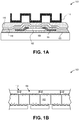
- An example of such a laminated photovoltaic system is provided in Figures 1A and 1B .
- a typical laminated solar cell package 100 includes an array of semiconductor solar cells 102 joined by metal interconnects 104 that are encapsulated within a polymer layer 106 between a glass superstrate 108 and a flexible polymer backsheet 110.
- a bypass diode 112 between cell interconnects 104 as well as a heat sink 114 (via a thermal adhesive 116) may also be integrated, as shown in Figures 1A and IB.
- Laminated solar cell packages also contemplated herein are solar cell packages such as those described in U.S. patent application 12/844,594 assigned to SunPower Corporation, entitled “Optoelectronic Device with Bypass Diode,” filed on July 27, 2010.
- a photovoltaic designer may focus on the thermal expansion mismatch of the glass, copper interconnects and silicon cells as the primary stress driver during thermal excursions, relying on the soft polymer encapsulant as a stress relieving feature.
- the soft polymer encapsulant may have a relatively high thermal expansion coefficient several times larger than glass and metals. During these conditions, the typically soft encapsulant may become a major stress driver in the package.
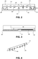
- Figure 2 illustrates a plan view of an interconnect for an optoelectronic device, in accordance with an embodiment of the present invention.
- an interconnect 200 includes an interconnect body 202 having an inner surface 204, an outer surface 206, a first end 208, and a second end 210.
- a plurality of bond pads 212 is coupled to the inner surface 204 of the interconnect body 202, between the first and second ends 208 and 210, respectively.
- one or more stress relief features are formed in the interconnect body 202, as described in more detail below.
- the stress relief feature of interconnect 200 can comprise a narrow slot C1 positioned in a location approximately equally between the first and second ends 208 and 210, respectively.
- the narrow slot C1 includes an opening at the inner surface 204 of the interconnect body 202 and extending into the interconnect body 202, but not through to the outer surface 206.
- feature C1 is a narrow slot cut into the center of the interconnect 200 that allows the bending of the interconnect at its mid-plane as needed if two cells (e.g., cells 250 and 252 partially depicted in Figure 2 ) to which it is rigidly connected rotate to form an effective V-shape (see arrow below C1 in Figure 2 ). Such rotation may be common given the periodic placement of interconnects down a linear array of cells, as depicted in Figure IB.
- the length of C1 is determined based on the expected displacement of the cells and the maximum allowable stress in the interconnects and bond pads coupled to the cells.
- feature C1 is typically around 7 millimeters for a 12 millimeter wide interconnect.
- the width of C1 is determined based on the manufacturing tolerances associated with punching or stamping operations as well as the need to reduce stress at the tip of the narrow slot.
- a typical width for feature C1 is approximately in the range of 0.5 - 1 millimeters, and the tip is a fully rounded semicircle to reduce stress concentrations.
- a small width may also limit the length of an Ohmic bottleneck, which may conduct the full photocurrent of a string of cells.
- the stress relief feature of interconnect 200 is a plurality of T-shaped slots C2, each T-shaped slot C2 approximately aligned with a corresponding one of the plurality of bond pads 212.
- the vertical portion 220 of each T-shaped slot C2 is proximate to the corresponding one of the plurality of bond pads 212, and the horizontal portion 222 of each T-shaped slot C2 is distal from the corresponding one of the plurality of bond pads 212.
- feature C2 is a T-shaped slot in the interconnect 200 that allows both rotation and normal displacement of the interconnect 200 relative to a cell (e.g., cell 250 or 252).
- a cell e.g., cell 250 or 252
- an encapsulant may approach its glass transition temperature and, due to its high thermal expansion coefficient, act as a stress driver. Surprisingly, in this condition, the encapsulant may pull an interconnect closer to a cell.
- feature C2 thus allows for a small deformation of the interconnect 200 towards a cell to relax strain in the encapsulant, limiting the stress at the cell-interconnect bond.
- each of the three connections to a cell contributes approximately one-third of the cumulative photocurrent being conducted in the string. Between and below these connections, the current may flow substantially in the wider portion of the interconnect 200 below the C2 features. As such, an a particular embodiment, the I 2 R losses associated with such features are low.
- the stress relief feature of interconnect 200 further comprises a vertical jog C3 near to or at the location where one of the plurality of bond pads 212 is coupled to the inner surface of the interconnect body 202.
- Figure 3 illustrates a cross-sectional view of an interconnect for an optoelectronic device highlighting a vertical jog, in accordance with an embodiment of the present invention.
- feature C3 is a vertical jog in the interconnect 200 that creates an out-of-plane mechanical coupling that reduces stress when the interconnect 200 is pulled closer to a cell (e.g., cell 252) by an encapsulant 390.
- the thinner region not only further reduces the stress between the cell 252 and interconnect 200 but also reduces vertical height differential between a heat sink 392, cell 252, and interconnect 200, reducing thermal resistance from the cell 252 and an associated diode to ambient.
- solder performs 499 can be added to the cell bond pads 212 of the interconnect 200.
- the stringing or wiring of an array of cells can be performed at a much higher throughput and with a much tighter process control than by dispensing solder paste during cell-to-interconnect soldering.
- the stress relief feature of interconnect 200 is a combination of slots D1.
- D1 includes a first narrow slot in a location proximate to the second end 210 and distal from the first end 208 of interconnect 200.
- the first narrow slot includes an opening at the outer surface 206 of the interconnect body 202 and extending into the interconnect body 202, but not through to the inner surface 204.
- D1 also includes a second narrow slot between the first narrow slot and the second end 210.
- the second narrow slot is between and orthogonal to the inner and outer surfaces 204 and 206, respectively, but does not open into either of the inner and outer surfaces 204 and 206.
- the second narrow slot is coupled to the horizontal portion of an outer-most T-shaped slot C2 of the plurality of T-shaped slots, as depicted in Figure 2 .
- feature D 1 is specifically designed to allow the ends 208 and 210 of the interconnect 200 to extend or retract to reduce stress on a diode package and to reduce any long-range stresses that might develop down an entire length of an array of cells.
- feature D 1 includes both the straight slot from the outside edge 206 of the interconnect 200 and the additional slot added to the T-shaped slot C2 at each bond pad 212.
- feature D 1 also allows expansion of the joints between a diode and interconnect 200 during the soldering or bonding assembly operations. If a soldering step is used to attach the diodes without feature Dl, stress may increase as the components cool down from the soldering temperature. In a particular embodiment, for a long string of several interconnects and diodes, such stress is otherwise appreciable and would otherwise result in early failure of the diodes during lamination as well as in displacement of the cells from nominal positions.
- feature D1 in the standard operating mode of the cells, has a minimal electrical impact on the circuit as there is nearly zero electrical current flowing through the diode.
- the cell connections are oriented such that the outermost regions (left and right ends) of the interconnect 200 conduct approximately one-third of the cumulative photocurrent generated by the cells.
- the I 2 R losses near feature D 1 are substantially less than they would be if this feature were placed closer to the center of the interconnect 200 where a higher current always flows even when the diode is not in bypass mode.
- the full string photocurrent may flow through and around feature D1.
- D1 becomes a larger source of electrical losses. However, these losses are small compared to the power dissipation otherwise within the diode in bypass mode.
- interconnect 200 includes a feature T1 formed in the interconnect body 202.
- the feature T1 includes a first L-shaped extension at the first end 208 of the interconnect body 202, and a second L-shaped extension at the second end 210 of the interconnect body 202.
- the horizontal bases of each of the first and second L-shaped extensions are proximate to the inner surface 204 and distal from the outer surface 206 of the interconnect body 202.
- feature TI is designed to increase thermal coupling between a diode and a heat sink that extends partially over the interconnect 202.
- Figure 5 illustrates an isometric view of a portion of an optoelectronic system with an internal bypass diode, in accordance with an embodiment of the present invention.
- the L-shaped extension (or pair of extensions) to the interconnect 200 allows additional heat sink 392 fin coupling in close proximity to a diode (e.g., a cell 500 bypass diode) 502, thus reducing the thermal gradient to ambient for a diode operating in bypass mode.
- the reduced temperature of the diode 502 also helps reduce any thermal stress that would develop due to an otherwise localized hot spot.
- the L-shaped extension is an extended area for increased thermal coupling between an interconnect and a heat sink mounted to an optoelectronic system.
- an interconnect contemplated herein is a coupling interconnect.
- the coupling interconnect may be used to couple two optoelectronic cells, as described above in association with Figures 2, 4 and 5 .
- the interconnect is a terminal interconnect.
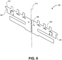
- Figure 6 illustrates a coupling interconnect that can be split to provide a pair of terminal interconnects, in accordance with an embodiment of the present invention.
- a coupling interconnect 600 includes a first half 602 and a second, symmetrical half 604 joined at a location 606 with the first half 602.
- Coupling interconnect 600 includes stress relief features 608 and other features described above, such as L-shaped features 610.
- Coupling interconnect 600 may be split along axis 612 to provide two terminal interconnects.
- an optoelectronic system includes a plurality of pairs of optoelectronic devices.
- each optoelectronic device is a back-contact solar cell.
- the optoelectronic system also includes a plurality of bypass diodes, one or more of the bypass diodes disposed between each of the pairs of optoelectronic devices.
- the optoelectronic system also includes a plurality of heat spreader units, one or more of the heat spreader units disposed above, and extending over, each of the bypass diodes.
- the optoelectronic system also includes a plurality of heat sinks, one or more of the heat sinks disposed above each of the heat spreader units.
- the optoelectronic system, interconnects or pairs of interconnects are disposed between pairs of optoelectronic devices, such as pairs of solar cells.
- one or more of the interconnects has one or more of a stress relief feature and an L-shaped feature, such as the stress relief features and L-shaped features described above in association with interconnects 200 and 600.
- a method of fabricating an interconnect for an optoelectronic device includes forming an interconnect body having an inner surface, an outer surface, a first end, a second end, and a plurality of bond pads coupled to the inner surface of the interconnect body, between the first and second ends.
- the method further includes forming one or more stress relief features and L-shaped features in the interconnect body, such as the stress relief features and L-shaped features described above in association with interconnects 200 and 600.
Claims (7)
- Interconnexion pour un dispositif optoélectronique, l'interconnexion comprenant : un corps d'interconnexion (202) comprenant une surface interne (204), une surface externe (206), une première extrémité (208) et une seconde extrémité (210) ; une pluralité de plots de connexion (212) couplés à la surface interne (204) du corps d'interconnexion (202), entre les première et seconde extrémités (208, 210); caractérisée par une caractéristique de soulagement de contrainte formée dans le corps d'interconnexion (202), la caractéristique de soulagement de contrainte comprenant une pluralité de fentes en forme de T (C2), chaque fente en forme de T (C2) étant approximativement alignée avec l'une correspondante de la pluralité de plots de connexion (212), la partie verticale (220) de chaque fente en forme de T (C2) étant proximale à l'un des plots de connexion (212) correspondants et la partie horizontale (222) de chaque fente en forme de T (C2) étant distale à celle correspondante de la pluralité de plots de connexion (212).
- Interconnexion selon la revendication 1, comprenant en outre : une première extension en forme de L au niveau de la première extrémité (208) du corps d'interconnexion (202) ; et une seconde extension en forme de L au niveau de la seconde extrémité (210) du corps d'interconnexion (202), les bases horizontales de chacune des première et seconde extensions en forme de L étant proximales à la surface interne (204) et distales de la surface externe (206) du corps d'interconnexion (202).
- Interconnexion selon la revendication 1 ou 2, dans laquelle la caractéristique de soulagement de contrainte comprend en outre une fente étroite (C1) dans un emplacement approximativement égal entre les première et seconde extrémités (208, 210), la fente étroite (C1) comprenant une ouverture au niveau de la surface interne (204) du corps d'interconnexion (202) et s'étendant dans le corps d'interconnexion (202), mais pas à travers la surface externe (206).
- Interconnexion selon la revendication 1 ou 2, dans laquelle la caractéristique de soulagement de contrainte comprend en outre : une première fente étroite dans un emplacement proximal à la première extrémité (208) et distal de la seconde extrémité (210), la première fente étroite comprenant une ouverture au niveau de la surface externe (206) du corps d'interconnexion (202) et s'étendant dans le corps d'interconnexion (202), mais pas à travers la surface interne (204) et
une seconde fente étroite entre la première fente étroite et la première extrémité (208), la seconde fente étroite étant entre et orthogonale aux surfaces interne et externe (204, 206), mais ne s'ouvrant dans aucune des surfaces interne et externe (204, 206) et la seconde fente étroite étant couplée à la partie horizontale (222) d'une fente en forme de T la plus externe de la pluralité de fentes en forme de T (C2). - Interconnexion selon la revendication 1 ou 2, dans laquelle la caractéristique de soulagement de contrainte comprend en outre une course verticale (C3) proche ou au niveau de l'emplacement où l'un de la pluralité de plots de connexion (212) est couplé à la surface interne (204) du corps d'interconnexion (202).
- Interconnexion selon la revendication 1 ou 2, dans laquelle la caractéristique de soulagement de contrainte comprend en outre :une première fente étroite dans un emplacement approximativement égal entre les première et seconde extrémités (208, 210), la première fente étroite comprenant une ouverture au niveau de la surface interne (204) du corps d'interconnexion (202) et s'étendant dans le corps d'interconnexion (202), mais pas jusqu'à la surface externe (206) ;une deuxième fente étroite dans un emplacement proximal à la première extrémité (208) et distal de la seconde extrémité (210), la deuxième fente étroite comprenant une ouverture au niveau de la surface externe (206) du corps d'interconnexion (202) et s'étendant dans le corps d'interconnexion (202), mais pas à travers la surface interne (204) ;une troisième fente étroite entre la deuxième fente étroite et la première extrémité (208), la troisième fente étroite étant entre et orthogonale aux surfaces interne et externe (204, 206), mais ne s'ouvrant dans aucune des surfaces interne et externe (204, 206) et la troisième fente étroite étant couplée à la partie horizontale (222) d'une fente en forme de T la plus externe de la pluralité de fentes en forme de T (C2) ; etune course verticale (C3) proche ou au niveau de l'emplacement où l'un de la pluralité de plots de connexion (212) est couplé à la surface interne (204) du corps d'interconnexion (202).
- Interconnexion selon la revendication 1 ou 2, dans laquelle l'interconnexion est une interconnexion de couplage ou une interconnexion de borne.
Applications Claiming Priority (2)
| Application Number | Priority Date | Filing Date | Title |
|---|---|---|---|
| US12/893,765 US8426974B2 (en) | 2010-09-29 | 2010-09-29 | Interconnect for an optoelectronic device |
| PCT/US2011/044743 WO2012050652A1 (fr) | 2010-09-29 | 2011-07-20 | Interconnexion pour dispositif optoélectronique |
Publications (3)
| Publication Number | Publication Date |
|---|---|
| EP2622653A1 EP2622653A1 (fr) | 2013-08-07 |
| EP2622653A4 EP2622653A4 (fr) | 2016-04-13 |
| EP2622653B1 true EP2622653B1 (fr) | 2018-12-05 |
Family
ID=45869828
Family Applications (1)
| Application Number | Title | Priority Date | Filing Date |
|---|---|---|---|
| EP11832905.1A Active EP2622653B1 (fr) | 2010-09-29 | 2011-07-20 | Interconnexion pour dispositif optoélectronique |
Country Status (7)
| Country | Link |
|---|---|
| US (3) | US8426974B2 (fr) |
| EP (1) | EP2622653B1 (fr) |
| JP (2) | JP5846529B2 (fr) |
| KR (1) | KR101779241B1 (fr) |
| CN (2) | CN102823003B (fr) |
| AU (1) | AU2011314342B2 (fr) |
| WO (1) | WO2012050652A1 (fr) |
Families Citing this family (15)
| Publication number | Priority date | Publication date | Assignee | Title |
|---|---|---|---|---|
| US8530990B2 (en) * | 2009-07-20 | 2013-09-10 | Sunpower Corporation | Optoelectronic device with heat spreader unit |
| US8636198B1 (en) | 2012-09-28 | 2014-01-28 | Sunpower Corporation | Methods and structures for forming and improving solder joint thickness and planarity control features for solar cells |
| JP6352894B2 (ja) * | 2015-12-24 | 2018-07-04 | トヨタ自動車株式会社 | 太陽電池モジュール |
| USD822890S1 (en) | 2016-09-07 | 2018-07-10 | Felxtronics Ap, Llc | Lighting apparatus |
| US10775030B2 (en) | 2017-05-05 | 2020-09-15 | Flex Ltd. | Light fixture device including rotatable light modules |
| USD832494S1 (en) | 2017-08-09 | 2018-10-30 | Flex Ltd. | Lighting module heatsink |
| USD862777S1 (en) | 2017-08-09 | 2019-10-08 | Flex Ltd. | Lighting module wide distribution lens |
| USD877964S1 (en) | 2017-08-09 | 2020-03-10 | Flex Ltd. | Lighting module |
| USD833061S1 (en) | 2017-08-09 | 2018-11-06 | Flex Ltd. | Lighting module locking endcap |
| USD872319S1 (en) | 2017-08-09 | 2020-01-07 | Flex Ltd. | Lighting module LED light board |
| USD846793S1 (en) | 2017-08-09 | 2019-04-23 | Flex Ltd. | Lighting module locking mechanism |
| USD832495S1 (en) | 2017-08-18 | 2018-10-30 | Flex Ltd. | Lighting module locking mechanism |
| USD862778S1 (en) | 2017-08-22 | 2019-10-08 | Flex Ltd | Lighting module lens |
| USD888323S1 (en) | 2017-09-07 | 2020-06-23 | Flex Ltd | Lighting module wire guard |
| CN114203847B (zh) * | 2022-02-18 | 2022-07-15 | 浙江爱旭太阳能科技有限公司 | 一种背接触电池连接用异形焊带 |
Family Cites Families (46)
| Publication number | Priority date | Publication date | Assignee | Title |
|---|---|---|---|---|
| US3340096A (en) * | 1962-02-26 | 1967-09-05 | Spectrolab A Division Of Textr | Solar cell array |
| US3454774A (en) * | 1965-09-10 | 1969-07-08 | Globe Union Inc | Electrical connector for semiconductor devices |
| ES491243A0 (es) | 1979-05-08 | 1980-12-16 | Saint Gobain Vitrage | Procedimiento de fabricacion de paneles de fotopilas solares |
| US4987474A (en) * | 1987-09-18 | 1991-01-22 | Hitachi, Ltd. | Semiconductor device and method of manufacturing the same |
| US4927770A (en) | 1988-11-14 | 1990-05-22 | Electric Power Research Inst. Corp. Of District Of Columbia | Method of fabricating back surface point contact solar cells |
| US5053083A (en) | 1989-05-08 | 1991-10-01 | The Board Of Trustees Of The Leland Stanford Junior University | Bilevel contact solar cells |
| US5011544A (en) | 1989-09-08 | 1991-04-30 | Solarex Corporation | Solar panel with interconnects and masking structure, and method |
| US5184019A (en) | 1990-03-16 | 1993-02-02 | The United States Of America As Represented By The United States Department Of Energy | Long range alpha particle detector |
| US5100808A (en) | 1990-08-15 | 1992-03-31 | Spectrolab, Inc. | Method of fabricating solar cell with integrated interconnect |
| US5185042A (en) | 1991-08-01 | 1993-02-09 | Trw Inc. | Generic solar cell array using a printed circuit substrate |
| US5139427A (en) * | 1991-09-23 | 1992-08-18 | Amp Incorporated | Planar array connector and flexible contact therefor |
| US5391235A (en) * | 1992-03-31 | 1995-02-21 | Canon Kabushiki Kaisha | Solar cell module and method of manufacturing the same |
| US5369291A (en) | 1993-03-29 | 1994-11-29 | Sunpower Corporation | Voltage controlled thyristor |
| US5360990A (en) | 1993-03-29 | 1994-11-01 | Sunpower Corporation | P/N junction device having porous emitter |
| US5468652A (en) | 1993-07-14 | 1995-11-21 | Sandia Corporation | Method of making a back contacted solar cell |
| JP3618802B2 (ja) | 1994-11-04 | 2005-02-09 | キヤノン株式会社 | 太陽電池モジュール |
| JP3488570B2 (ja) * | 1996-03-29 | 2004-01-19 | ローム株式会社 | Led発光装置およびこれを用いた面発光照明装置 |
| JP3680490B2 (ja) * | 1997-05-29 | 2005-08-10 | 富士電機アドバンストテクノロジー株式会社 | 可撓性太陽電池モジュール |
| US5972732A (en) | 1997-12-19 | 1999-10-26 | Sandia Corporation | Method of monolithic module assembly |
| US6278054B1 (en) | 1998-05-28 | 2001-08-21 | Tecstar Power Systems, Inc. | Solar cell having an integral monolithically grown bypass diode |
| JP2000323208A (ja) | 1999-03-10 | 2000-11-24 | Sharp Corp | インターコネクタ、その形成方法およびその接合装置 |
| US6274402B1 (en) | 1999-12-30 | 2001-08-14 | Sunpower Corporation | Method of fabricating a silicon solar cell |
| US6337283B1 (en) | 1999-12-30 | 2002-01-08 | Sunpower Corporation | Method of fabricating a silicon solar cell |
| US6387726B1 (en) | 1999-12-30 | 2002-05-14 | Sunpower Corporation | Method of fabricating a silicon solar cell |
| US6423568B1 (en) | 1999-12-30 | 2002-07-23 | Sunpower Corporation | Method of fabricating a silicon solar cell |
| US6313395B1 (en) | 2000-04-24 | 2001-11-06 | Sunpower Corporation | Interconnect structure for solar cells and method of making same |
| JP2001339091A (ja) | 2000-05-29 | 2001-12-07 | Fuji Electric Co Ltd | 薄膜太陽電池モジュールとその応力監視方法 |
| US6333457B1 (en) | 2000-08-29 | 2001-12-25 | Sunpower Corporation | Edge passivated silicon solar/photo cell and method of manufacture |
| JP4137415B2 (ja) | 2000-11-21 | 2008-08-20 | シャープ株式会社 | 太陽電池セルの交換方法 |
| DE10139441C1 (de) | 2001-08-10 | 2002-10-10 | Astrium Gmbh | Verfahren zur Reparatur eines Solar-Panels |
| US6713670B2 (en) | 2001-08-17 | 2004-03-30 | Composite Optics, Incorporated | Electrostatically clean solar array |
| KR101252838B1 (ko) | 2003-04-04 | 2013-04-09 | 비피 코포레이션 노쓰 아메리카 인코포레이티드 | 태양광 발전기에 대한 성능 모니터 |
| JP4393303B2 (ja) * | 2003-09-05 | 2010-01-06 | キヤノン株式会社 | 半導体装置の製造方法 |
| US7378742B2 (en) * | 2004-10-27 | 2008-05-27 | Intel Corporation | Compliant interconnects for semiconductors and micromachines |
| US7390961B2 (en) * | 2004-06-04 | 2008-06-24 | Sunpower Corporation | Interconnection of solar cells in a solar cell module |
| DE102004038112B4 (de) | 2004-08-05 | 2006-11-16 | Siemens Ag | Elektrisches Schaltgerät |
| DE102004050269A1 (de) | 2004-10-14 | 2006-04-20 | Institut Für Solarenergieforschung Gmbh | Verfahren zur Kontakttrennung elektrisch leitfähiger Schichten auf rückkontaktierten Solarzellen und Solarzelle |
| JP4182063B2 (ja) * | 2005-01-24 | 2008-11-19 | トヤマキカイ株式会社 | リード構造 |
| US7154361B2 (en) | 2005-05-04 | 2006-12-26 | General Electric Company | Accessories for a rotatable latching shaft of a circuit breaker |
| US7148774B1 (en) | 2005-07-11 | 2006-12-12 | Eaton Corporation | Contact assembly |
| US7732705B2 (en) * | 2005-10-11 | 2010-06-08 | Emcore Solar Power, Inc. | Reliable interconnection of solar cells including integral bypass diode |
| JP4986462B2 (ja) * | 2006-01-27 | 2012-07-25 | シャープ株式会社 | 太陽電池ストリングおよびその製造方法、ならびに、その太陽電池ストリングを用いる太陽電池モジュール |
| US8148627B2 (en) * | 2006-08-25 | 2012-04-03 | Sunpower Corporation | Solar cell interconnect with multiple current paths |
| US20080216887A1 (en) * | 2006-12-22 | 2008-09-11 | Advent Solar, Inc. | Interconnect Technologies for Back Contact Solar Cells and Modules |
| US20090139557A1 (en) * | 2007-11-30 | 2009-06-04 | Douglas Rose | Busbar connection configuration to accommodate for cell misalignment |
| US8636198B1 (en) * | 2012-09-28 | 2014-01-28 | Sunpower Corporation | Methods and structures for forming and improving solder joint thickness and planarity control features for solar cells |
-
2010
- 2010-09-29 US US12/893,765 patent/US8426974B2/en active Active
-
2011
- 2011-07-20 JP JP2013531574A patent/JP5846529B2/ja not_active Expired - Fee Related
- 2011-07-20 WO PCT/US2011/044743 patent/WO2012050652A1/fr active Application Filing
- 2011-07-20 AU AU2011314342A patent/AU2011314342B2/en active Active
- 2011-07-20 CN CN201180016615.8A patent/CN102823003B/zh active Active
- 2011-07-20 KR KR1020137010753A patent/KR101779241B1/ko active IP Right Grant
- 2011-07-20 EP EP11832905.1A patent/EP2622653B1/fr active Active
- 2011-07-20 CN CN201610076785.XA patent/CN105679855B/zh active Active
-
2013
- 2013-04-01 US US13/854,607 patent/US8786095B2/en active Active
-
2014
- 2014-06-13 US US14/303,854 patent/US9537036B2/en active Active
-
2015
- 2015-11-13 JP JP2015223173A patent/JP6159978B2/ja not_active Expired - Fee Related
Non-Patent Citations (1)
| Title |
|---|
| None * |
Also Published As
| Publication number | Publication date |
|---|---|
| US8786095B2 (en) | 2014-07-22 |
| WO2012050652A1 (fr) | 2012-04-19 |
| KR20140009976A (ko) | 2014-01-23 |
| EP2622653A4 (fr) | 2016-04-13 |
| CN105679855B (zh) | 2017-07-28 |
| EP2622653A1 (fr) | 2013-08-07 |
| US20130228906A1 (en) | 2013-09-05 |
| CN102823003A (zh) | 2012-12-12 |
| JP2013539232A (ja) | 2013-10-17 |
| US20140291852A1 (en) | 2014-10-02 |
| JP2016054307A (ja) | 2016-04-14 |
| KR101779241B1 (ko) | 2017-09-18 |
| US9537036B2 (en) | 2017-01-03 |
| CN102823003B (zh) | 2016-03-09 |
| CN105679855A (zh) | 2016-06-15 |
| US20120074576A1 (en) | 2012-03-29 |
| AU2011314342A1 (en) | 2013-05-02 |
| US8426974B2 (en) | 2013-04-23 |
| AU2011314342B2 (en) | 2014-07-10 |
| JP5846529B2 (ja) | 2016-01-20 |
| JP6159978B2 (ja) | 2017-07-12 |
Similar Documents
| Publication | Publication Date | Title |
|---|---|---|
| EP2622653B1 (fr) | Interconnexion pour dispositif optoélectronique | |
| US9685573B2 (en) | Diode and heat spreader for solar module | |
| US10483421B2 (en) | Solar cell module | |
| US8586857B2 (en) | Combined diode, lead assembly incorporating an expansion joint | |
| US9947820B2 (en) | Shingled solar cell panel employing hidden taps | |
| US8860162B2 (en) | Optoelectronic device with heat spreader unit | |
| US20110192448A1 (en) | Solar-cell module with in-laminate diodes and external-connection mechanisms mounted to respective edge regions | |
| US20120006483A1 (en) | Methods for Interconnecting Solar Cells | |
| EP2879188B1 (fr) | Cellule solaire et son procédé de fabrication | |
| CN102683446A (zh) | 太阳能光伏电池组件保护用二极管模块 | |
| US20170162723A1 (en) | Spot-welded and adhesive-bonded interconnects for solar cells |
Legal Events
| Date | Code | Title | Description |
|---|---|---|---|
| PUAI | Public reference made under article 153(3) epc to a published international application that has entered the european phase |
Free format text: ORIGINAL CODE: 0009012 |
|
| 17P | Request for examination filed |
Effective date: 20130313 |
|
| AK | Designated contracting states |
Kind code of ref document: A1 Designated state(s): AL AT BE BG CH CY CZ DE DK EE ES FI FR GB GR HR HU IE IS IT LI LT LU LV MC MK MT NL NO PL PT RO RS SE SI SK SM TR |
|
| DAX | Request for extension of the european patent (deleted) | ||
| RIC1 | Information provided on ipc code assigned before grant |
Ipc: H01L 31/04 20140101ALI20151119BHEP Ipc: H01L 33/36 20100101ALI20151119BHEP Ipc: H01L 33/62 20100101AFI20151119BHEP |
|
| RA4 | Supplementary search report drawn up and despatched (corrected) |
Effective date: 20160316 |
|
| RIC1 | Information provided on ipc code assigned before grant |
Ipc: H01L 33/36 20100101ALI20160310BHEP Ipc: H01L 33/62 20100101AFI20160310BHEP Ipc: H01L 31/04 20060101ALI20160310BHEP |
|
| STAA | Information on the status of an ep patent application or granted ep patent |
Free format text: STATUS: EXAMINATION IS IN PROGRESS |
|
| 17Q | First examination report despatched |
Effective date: 20171018 |
|
| RIC1 | Information provided on ipc code assigned before grant |
Ipc: H01L 33/62 20100101AFI20180516BHEP |
|
| GRAP | Despatch of communication of intention to grant a patent |
Free format text: ORIGINAL CODE: EPIDOSNIGR1 |
|
| STAA | Information on the status of an ep patent application or granted ep patent |
Free format text: STATUS: GRANT OF PATENT IS INTENDED |
|
| INTG | Intention to grant announced |
Effective date: 20180622 |
|
| GRAS | Grant fee paid |
Free format text: ORIGINAL CODE: EPIDOSNIGR3 |
|
| GRAA | (expected) grant |
Free format text: ORIGINAL CODE: 0009210 |
|
| GRAA | (expected) grant |
Free format text: ORIGINAL CODE: 0009210 |
|
| STAA | Information on the status of an ep patent application or granted ep patent |
Free format text: STATUS: THE PATENT HAS BEEN GRANTED |
|
| AK | Designated contracting states |
Kind code of ref document: B1 Designated state(s): AL AT BE BG CH CY CZ DE DK EE ES FI FR GB GR HR HU IE IS IT LI LT LU LV MC MK MT NL NO PL PT RO RS SE SI SK SM TR |
|
| RAP1 | Party data changed (applicant data changed or rights of an application transferred) |
Owner name: SUNPOWER CORPORATION |
|
| REG | Reference to a national code |
Ref country code: GB Ref legal event code: FG4D |
|
| REG | Reference to a national code |
Ref country code: CH Ref legal event code: EP |
|
| REG | Reference to a national code |
Ref country code: AT Ref legal event code: REF Ref document number: 1074151 Country of ref document: AT Kind code of ref document: T Effective date: 20181215 |
|
| REG | Reference to a national code |
Ref country code: IE Ref legal event code: FG4D |
|
| REG | Reference to a national code |
Ref country code: DE Ref legal event code: R096 Ref document number: 602011054617 Country of ref document: DE |
|
| REG | Reference to a national code |
Ref country code: NL Ref legal event code: MP Effective date: 20181205 |
|
| REG | Reference to a national code |
Ref country code: AT Ref legal event code: MK05 Ref document number: 1074151 Country of ref document: AT Kind code of ref document: T Effective date: 20181205 |
|
| REG | Reference to a national code |
Ref country code: LT Ref legal event code: MG4D |
|
| PG25 | Lapsed in a contracting state [announced via postgrant information from national office to epo] |
Ref country code: LV Free format text: LAPSE BECAUSE OF FAILURE TO SUBMIT A TRANSLATION OF THE DESCRIPTION OR TO PAY THE FEE WITHIN THE PRESCRIBED TIME-LIMIT Effective date: 20181205 Ref country code: ES Free format text: LAPSE BECAUSE OF FAILURE TO SUBMIT A TRANSLATION OF THE DESCRIPTION OR TO PAY THE FEE WITHIN THE PRESCRIBED TIME-LIMIT Effective date: 20181205 Ref country code: BG Free format text: LAPSE BECAUSE OF FAILURE TO SUBMIT A TRANSLATION OF THE DESCRIPTION OR TO PAY THE FEE WITHIN THE PRESCRIBED TIME-LIMIT Effective date: 20190305 Ref country code: LT Free format text: LAPSE BECAUSE OF FAILURE TO SUBMIT A TRANSLATION OF THE DESCRIPTION OR TO PAY THE FEE WITHIN THE PRESCRIBED TIME-LIMIT Effective date: 20181205 Ref country code: HR Free format text: LAPSE BECAUSE OF FAILURE TO SUBMIT A TRANSLATION OF THE DESCRIPTION OR TO PAY THE FEE WITHIN THE PRESCRIBED TIME-LIMIT Effective date: 20181205 Ref country code: FI Free format text: LAPSE BECAUSE OF FAILURE TO SUBMIT A TRANSLATION OF THE DESCRIPTION OR TO PAY THE FEE WITHIN THE PRESCRIBED TIME-LIMIT Effective date: 20181205 Ref country code: NO Free format text: LAPSE BECAUSE OF FAILURE TO SUBMIT A TRANSLATION OF THE DESCRIPTION OR TO PAY THE FEE WITHIN THE PRESCRIBED TIME-LIMIT Effective date: 20190305 Ref country code: AT Free format text: LAPSE BECAUSE OF FAILURE TO SUBMIT A TRANSLATION OF THE DESCRIPTION OR TO PAY THE FEE WITHIN THE PRESCRIBED TIME-LIMIT Effective date: 20181205 |
|
| PG25 | Lapsed in a contracting state [announced via postgrant information from national office to epo] |
Ref country code: RS Free format text: LAPSE BECAUSE OF FAILURE TO SUBMIT A TRANSLATION OF THE DESCRIPTION OR TO PAY THE FEE WITHIN THE PRESCRIBED TIME-LIMIT Effective date: 20181205 Ref country code: GR Free format text: LAPSE BECAUSE OF FAILURE TO SUBMIT A TRANSLATION OF THE DESCRIPTION OR TO PAY THE FEE WITHIN THE PRESCRIBED TIME-LIMIT Effective date: 20190306 Ref country code: AL Free format text: LAPSE BECAUSE OF FAILURE TO SUBMIT A TRANSLATION OF THE DESCRIPTION OR TO PAY THE FEE WITHIN THE PRESCRIBED TIME-LIMIT Effective date: 20181205 Ref country code: SE Free format text: LAPSE BECAUSE OF FAILURE TO SUBMIT A TRANSLATION OF THE DESCRIPTION OR TO PAY THE FEE WITHIN THE PRESCRIBED TIME-LIMIT Effective date: 20181205 |
|
| PG25 | Lapsed in a contracting state [announced via postgrant information from national office to epo] |
Ref country code: NL Free format text: LAPSE BECAUSE OF FAILURE TO SUBMIT A TRANSLATION OF THE DESCRIPTION OR TO PAY THE FEE WITHIN THE PRESCRIBED TIME-LIMIT Effective date: 20181205 |
|
| PG25 | Lapsed in a contracting state [announced via postgrant information from national office to epo] |
Ref country code: IT Free format text: LAPSE BECAUSE OF FAILURE TO SUBMIT A TRANSLATION OF THE DESCRIPTION OR TO PAY THE FEE WITHIN THE PRESCRIBED TIME-LIMIT Effective date: 20181205 Ref country code: PT Free format text: LAPSE BECAUSE OF FAILURE TO SUBMIT A TRANSLATION OF THE DESCRIPTION OR TO PAY THE FEE WITHIN THE PRESCRIBED TIME-LIMIT Effective date: 20190405 Ref country code: CZ Free format text: LAPSE BECAUSE OF FAILURE TO SUBMIT A TRANSLATION OF THE DESCRIPTION OR TO PAY THE FEE WITHIN THE PRESCRIBED TIME-LIMIT Effective date: 20181205 Ref country code: PL Free format text: LAPSE BECAUSE OF FAILURE TO SUBMIT A TRANSLATION OF THE DESCRIPTION OR TO PAY THE FEE WITHIN THE PRESCRIBED TIME-LIMIT Effective date: 20181205 |
|
| PG25 | Lapsed in a contracting state [announced via postgrant information from national office to epo] |
Ref country code: RO Free format text: LAPSE BECAUSE OF FAILURE TO SUBMIT A TRANSLATION OF THE DESCRIPTION OR TO PAY THE FEE WITHIN THE PRESCRIBED TIME-LIMIT Effective date: 20181205 Ref country code: SK Free format text: LAPSE BECAUSE OF FAILURE TO SUBMIT A TRANSLATION OF THE DESCRIPTION OR TO PAY THE FEE WITHIN THE PRESCRIBED TIME-LIMIT Effective date: 20181205 Ref country code: IS Free format text: LAPSE BECAUSE OF FAILURE TO SUBMIT A TRANSLATION OF THE DESCRIPTION OR TO PAY THE FEE WITHIN THE PRESCRIBED TIME-LIMIT Effective date: 20190405 Ref country code: EE Free format text: LAPSE BECAUSE OF FAILURE TO SUBMIT A TRANSLATION OF THE DESCRIPTION OR TO PAY THE FEE WITHIN THE PRESCRIBED TIME-LIMIT Effective date: 20181205 Ref country code: SM Free format text: LAPSE BECAUSE OF FAILURE TO SUBMIT A TRANSLATION OF THE DESCRIPTION OR TO PAY THE FEE WITHIN THE PRESCRIBED TIME-LIMIT Effective date: 20181205 |
|
| REG | Reference to a national code |
Ref country code: DE Ref legal event code: R097 Ref document number: 602011054617 Country of ref document: DE |
|
| PLBE | No opposition filed within time limit |
Free format text: ORIGINAL CODE: 0009261 |
|
| STAA | Information on the status of an ep patent application or granted ep patent |
Free format text: STATUS: NO OPPOSITION FILED WITHIN TIME LIMIT |
|
| PG25 | Lapsed in a contracting state [announced via postgrant information from national office to epo] |
Ref country code: SI Free format text: LAPSE BECAUSE OF FAILURE TO SUBMIT A TRANSLATION OF THE DESCRIPTION OR TO PAY THE FEE WITHIN THE PRESCRIBED TIME-LIMIT Effective date: 20181205 Ref country code: DK Free format text: LAPSE BECAUSE OF FAILURE TO SUBMIT A TRANSLATION OF THE DESCRIPTION OR TO PAY THE FEE WITHIN THE PRESCRIBED TIME-LIMIT Effective date: 20181205 |
|
| 26N | No opposition filed |
Effective date: 20190906 |
|
| PG25 | Lapsed in a contracting state [announced via postgrant information from national office to epo] |
Ref country code: MC Free format text: LAPSE BECAUSE OF FAILURE TO SUBMIT A TRANSLATION OF THE DESCRIPTION OR TO PAY THE FEE WITHIN THE PRESCRIBED TIME-LIMIT Effective date: 20181205 |
|
| REG | Reference to a national code |
Ref country code: CH Ref legal event code: PL |
|
| GBPC | Gb: european patent ceased through non-payment of renewal fee |
Effective date: 20190720 |
|
| PG25 | Lapsed in a contracting state [announced via postgrant information from national office to epo] |
Ref country code: TR Free format text: LAPSE BECAUSE OF FAILURE TO SUBMIT A TRANSLATION OF THE DESCRIPTION OR TO PAY THE FEE WITHIN THE PRESCRIBED TIME-LIMIT Effective date: 20181205 |
|
| REG | Reference to a national code |
Ref country code: BE Ref legal event code: MM Effective date: 20190731 |
|
| PG25 | Lapsed in a contracting state [announced via postgrant information from national office to epo] |
Ref country code: GB Free format text: LAPSE BECAUSE OF NON-PAYMENT OF DUE FEES Effective date: 20190720 |
|
| PG25 | Lapsed in a contracting state [announced via postgrant information from national office to epo] |
Ref country code: BE Free format text: LAPSE BECAUSE OF NON-PAYMENT OF DUE FEES Effective date: 20190731 Ref country code: LU Free format text: LAPSE BECAUSE OF NON-PAYMENT OF DUE FEES Effective date: 20190720 Ref country code: LI Free format text: LAPSE BECAUSE OF NON-PAYMENT OF DUE FEES Effective date: 20190731 Ref country code: CH Free format text: LAPSE BECAUSE OF NON-PAYMENT OF DUE FEES Effective date: 20190731 |
|
| PG25 | Lapsed in a contracting state [announced via postgrant information from national office to epo] |
Ref country code: FR Free format text: LAPSE BECAUSE OF NON-PAYMENT OF DUE FEES Effective date: 20190731 |
|
| PG25 | Lapsed in a contracting state [announced via postgrant information from national office to epo] |
Ref country code: IE Free format text: LAPSE BECAUSE OF NON-PAYMENT OF DUE FEES Effective date: 20190720 |
|
| PG25 | Lapsed in a contracting state [announced via postgrant information from national office to epo] |
Ref country code: CY Free format text: LAPSE BECAUSE OF FAILURE TO SUBMIT A TRANSLATION OF THE DESCRIPTION OR TO PAY THE FEE WITHIN THE PRESCRIBED TIME-LIMIT Effective date: 20181205 |
|
| PG25 | Lapsed in a contracting state [announced via postgrant information from national office to epo] |
Ref country code: MT Free format text: LAPSE BECAUSE OF FAILURE TO SUBMIT A TRANSLATION OF THE DESCRIPTION OR TO PAY THE FEE WITHIN THE PRESCRIBED TIME-LIMIT Effective date: 20181205 Ref country code: HU Free format text: LAPSE BECAUSE OF FAILURE TO SUBMIT A TRANSLATION OF THE DESCRIPTION OR TO PAY THE FEE WITHIN THE PRESCRIBED TIME-LIMIT; INVALID AB INITIO Effective date: 20110720 |
|
| REG | Reference to a national code |
Ref country code: DE Ref legal event code: R082 Ref document number: 602011054617 Country of ref document: DE Representative=s name: KRAUS & LEDERER PARTGMBB, DE Ref country code: DE Ref legal event code: R082 Ref document number: 602011054617 Country of ref document: DE Representative=s name: LEDERER & KELLER PATENTANWAELTE PARTNERSCHAFT , DE |
|
| REG | Reference to a national code |
Ref country code: DE Ref legal event code: R081 Ref document number: 602011054617 Country of ref document: DE Owner name: MAXEON SOLAR PTE. LTD., SG Free format text: FORMER OWNER: SUNPOWER CORPORATION, SAN JOSE, CALIF., US |
|
| PG25 | Lapsed in a contracting state [announced via postgrant information from national office to epo] |
Ref country code: MK Free format text: LAPSE BECAUSE OF FAILURE TO SUBMIT A TRANSLATION OF THE DESCRIPTION OR TO PAY THE FEE WITHIN THE PRESCRIBED TIME-LIMIT Effective date: 20181205 |
|
| PGFP | Annual fee paid to national office [announced via postgrant information from national office to epo] |
Ref country code: DE Payment date: 20230620 Year of fee payment: 13 |
|
| REG | Reference to a national code |
Ref country code: DE Ref legal event code: R082 Ref document number: 602011054617 Country of ref document: DE Representative=s name: KRAUS & LEDERER PARTGMBB, DE |