EP2620975A1 - Thin film production process and thin film production device - Google Patents
Thin film production process and thin film production device Download PDFInfo
- Publication number
- EP2620975A1 EP2620975A1 EP11826558.6A EP11826558A EP2620975A1 EP 2620975 A1 EP2620975 A1 EP 2620975A1 EP 11826558 A EP11826558 A EP 11826558A EP 2620975 A1 EP2620975 A1 EP 2620975A1
- Authority
- EP
- European Patent Office
- Prior art keywords
- gas
- film
- raw material
- thin
- supply
- Prior art date
- Legal status (The legal status is an assumption and is not a legal conclusion. Google has not performed a legal analysis and makes no representation as to the accuracy of the status listed.)
- Withdrawn
Links
Images



Classifications
-
- C—CHEMISTRY; METALLURGY
- C01—INORGANIC CHEMISTRY
- C01G—COMPOUNDS CONTAINING METALS NOT COVERED BY SUBCLASSES C01D OR C01F
- C01G25/00—Compounds of zirconium
-
- C—CHEMISTRY; METALLURGY
- C23—COATING METALLIC MATERIAL; COATING MATERIAL WITH METALLIC MATERIAL; CHEMICAL SURFACE TREATMENT; DIFFUSION TREATMENT OF METALLIC MATERIAL; COATING BY VACUUM EVAPORATION, BY SPUTTERING, BY ION IMPLANTATION OR BY CHEMICAL VAPOUR DEPOSITION, IN GENERAL; INHIBITING CORROSION OF METALLIC MATERIAL OR INCRUSTATION IN GENERAL
- C23C—COATING METALLIC MATERIAL; COATING MATERIAL WITH METALLIC MATERIAL; SURFACE TREATMENT OF METALLIC MATERIAL BY DIFFUSION INTO THE SURFACE, BY CHEMICAL CONVERSION OR SUBSTITUTION; COATING BY VACUUM EVAPORATION, BY SPUTTERING, BY ION IMPLANTATION OR BY CHEMICAL VAPOUR DEPOSITION, IN GENERAL
- C23C16/00—Chemical coating by decomposition of gaseous compounds, without leaving reaction products of surface material in the coating, i.e. chemical vapour deposition [CVD] processes
- C23C16/22—Chemical coating by decomposition of gaseous compounds, without leaving reaction products of surface material in the coating, i.e. chemical vapour deposition [CVD] processes characterised by the deposition of inorganic material, other than metallic material
- C23C16/30—Deposition of compounds, mixtures or solid solutions, e.g. borides, carbides, nitrides
- C23C16/40—Oxides
- C23C16/409—Oxides of the type ABO3 with A representing alkali, alkaline earth metal or lead and B representing a refractory metal, nickel, scandium or a lanthanide
-
- C—CHEMISTRY; METALLURGY
- C23—COATING METALLIC MATERIAL; COATING MATERIAL WITH METALLIC MATERIAL; CHEMICAL SURFACE TREATMENT; DIFFUSION TREATMENT OF METALLIC MATERIAL; COATING BY VACUUM EVAPORATION, BY SPUTTERING, BY ION IMPLANTATION OR BY CHEMICAL VAPOUR DEPOSITION, IN GENERAL; INHIBITING CORROSION OF METALLIC MATERIAL OR INCRUSTATION IN GENERAL
- C23C—COATING METALLIC MATERIAL; COATING MATERIAL WITH METALLIC MATERIAL; SURFACE TREATMENT OF METALLIC MATERIAL BY DIFFUSION INTO THE SURFACE, BY CHEMICAL CONVERSION OR SUBSTITUTION; COATING BY VACUUM EVAPORATION, BY SPUTTERING, BY ION IMPLANTATION OR BY CHEMICAL VAPOUR DEPOSITION, IN GENERAL
- C23C16/00—Chemical coating by decomposition of gaseous compounds, without leaving reaction products of surface material in the coating, i.e. chemical vapour deposition [CVD] processes
- C23C16/44—Chemical coating by decomposition of gaseous compounds, without leaving reaction products of surface material in the coating, i.e. chemical vapour deposition [CVD] processes characterised by the method of coating
- C23C16/455—Chemical coating by decomposition of gaseous compounds, without leaving reaction products of surface material in the coating, i.e. chemical vapour deposition [CVD] processes characterised by the method of coating characterised by the method used for introducing gases into reaction chamber or for modifying gas flows in reaction chamber
-
- C—CHEMISTRY; METALLURGY
- C23—COATING METALLIC MATERIAL; COATING MATERIAL WITH METALLIC MATERIAL; CHEMICAL SURFACE TREATMENT; DIFFUSION TREATMENT OF METALLIC MATERIAL; COATING BY VACUUM EVAPORATION, BY SPUTTERING, BY ION IMPLANTATION OR BY CHEMICAL VAPOUR DEPOSITION, IN GENERAL; INHIBITING CORROSION OF METALLIC MATERIAL OR INCRUSTATION IN GENERAL
- C23C—COATING METALLIC MATERIAL; COATING MATERIAL WITH METALLIC MATERIAL; SURFACE TREATMENT OF METALLIC MATERIAL BY DIFFUSION INTO THE SURFACE, BY CHEMICAL CONVERSION OR SUBSTITUTION; COATING BY VACUUM EVAPORATION, BY SPUTTERING, BY ION IMPLANTATION OR BY CHEMICAL VAPOUR DEPOSITION, IN GENERAL
- C23C16/00—Chemical coating by decomposition of gaseous compounds, without leaving reaction products of surface material in the coating, i.e. chemical vapour deposition [CVD] processes
- C23C16/56—After-treatment
-
- H—ELECTRICITY
- H10—SEMICONDUCTOR DEVICES; ELECTRIC SOLID-STATE DEVICES NOT OTHERWISE PROVIDED FOR
- H10P—GENERIC PROCESSES OR APPARATUS FOR THE MANUFACTURE OR TREATMENT OF DEVICES COVERED BY CLASS H10
- H10P14/00—Formation of materials, e.g. in the shape of layers or pillars
- H10P14/60—Formation of materials, e.g. in the shape of layers or pillars of insulating materials
- H10P14/63—Formation of materials, e.g. in the shape of layers or pillars of insulating materials characterised by the formation processes
- H10P14/6326—Deposition processes
- H10P14/6328—Deposition from the gas or vapour phase
- H10P14/6334—Deposition from the gas or vapour phase using decomposition or reaction of gaseous or vapour phase compounds, i.e. chemical vapour deposition
-
- H—ELECTRICITY
- H10—SEMICONDUCTOR DEVICES; ELECTRIC SOLID-STATE DEVICES NOT OTHERWISE PROVIDED FOR
- H10P—GENERIC PROCESSES OR APPARATUS FOR THE MANUFACTURE OR TREATMENT OF DEVICES COVERED BY CLASS H10
- H10P14/00—Formation of materials, e.g. in the shape of layers or pillars
- H10P14/60—Formation of materials, e.g. in the shape of layers or pillars of insulating materials
- H10P14/69—Inorganic materials
- H10P14/692—Inorganic materials composed of oxides, glassy oxides or oxide-based glasses
- H10P14/6938—Inorganic materials composed of oxides, glassy oxides or oxide-based glasses the material containing at least one metal element, e.g. metal oxides, metal oxynitrides or metal oxycarbides
- H10P14/69398—Inorganic materials composed of oxides, glassy oxides or oxide-based glasses the material containing at least one metal element, e.g. metal oxides, metal oxynitrides or metal oxycarbides the material having a perovskite structure, e.g. BaTiO3
-
- C—CHEMISTRY; METALLURGY
- C01—INORGANIC CHEMISTRY
- C01P—INDEXING SCHEME RELATING TO STRUCTURAL AND PHYSICAL ASPECTS OF SOLID INORGANIC COMPOUNDS
- C01P2002/00—Crystal-structural characteristics
- C01P2002/30—Three-dimensional structures
- C01P2002/34—Three-dimensional structures perovskite-type (ABO3)
-
- C—CHEMISTRY; METALLURGY
- C01—INORGANIC CHEMISTRY
- C01P—INDEXING SCHEME RELATING TO STRUCTURAL AND PHYSICAL ASPECTS OF SOLID INORGANIC COMPOUNDS
- C01P2004/00—Particle morphology
- C01P2004/01—Particle morphology depicted by an image
- C01P2004/03—Particle morphology depicted by an image obtained by SEM
-
- C—CHEMISTRY; METALLURGY
- C01—INORGANIC CHEMISTRY
- C01P—INDEXING SCHEME RELATING TO STRUCTURAL AND PHYSICAL ASPECTS OF SOLID INORGANIC COMPOUNDS
- C01P2006/00—Physical properties of inorganic compounds
- C01P2006/40—Electric properties
-
- H—ELECTRICITY
- H10—SEMICONDUCTOR DEVICES; ELECTRIC SOLID-STATE DEVICES NOT OTHERWISE PROVIDED FOR
- H10D—INORGANIC ELECTRIC SEMICONDUCTOR DEVICES
- H10D1/00—Resistors, capacitors or inductors
- H10D1/60—Capacitors
- H10D1/68—Capacitors having no potential barriers
- H10D1/682—Capacitors having no potential barriers having dielectrics comprising perovskite structures
Definitions
- the present invention relates to a method of forming a dielectric thin-film such as a PZT (lead zirconate titanate) thin-film, and a thin-film forming apparatus.
- a dielectric thin-film such as a PZT (lead zirconate titanate) thin-film
- a ferroelectric thin-film for use in a ferroelectric random access memory (FeRAM) or the like a thin-film of lead zirconate titanate (Pb(Zr,Ti)O3; PZT) having a perovskite structure is known.
- Pb(Zr,Ti)O3; PZT lead zirconate titanate
- Such dielectric thin-film is formed by a Metal Organic Chemical Vapor Deposition (MOCVD) method.
- MOCVD Metal Organic Chemical Vapor Deposition
- the MOCVD method is a method of forming the dielectric thin-film by reacting a raw material organic metal gas with an oxidation gas at a high temperature.
- a self-alignment region where a composition ratio of the thin-film is less changed even if a flow rate of the raw material gas is changed.
- Patent Document 1 describes a MOCVD method of supplying a mixed gas of an organic metal raw material gas, an oxidation gas and a diluent gas to a substrate that has been heated.
- a combustible gas is also supplied when the mixed gas is supplied to the substrate.
- excess oxygen on the surface of the substrate is combusted and discharged, a high quality thin-film can be formed (see paragraphs [0011] and [0025] in Patent Document 1.
- Patent Document 1 Japanese Patent Application Laid-open No. 2004-273787
- the dielectric thin-film When the dielectric thin-film is formed as described above, the dielectric thin-film preferably has a small surface roughness. If the dielectric thin-film has a high surface roughness, the process of forming a ferroelectric memory having, for example, the dielectric thin-film may cause a problem. Also, there is a concern about that electrical properties of the dielectric thin-film are not sufficiently provided, for example.
- an object of the present invention is to provide a thin-film forming method and a thin-film forming apparatus, both of which enable the formation of a dielectric thin-film having a small surface roughness.
- a method of forming a thin-film comprises supplying a mixed gas to a substrate that is placed and heated in a chamber; the mixed gas containing a metal raw material gas that serves as a raw material for a dielectric thin-film having perovskite type crystals and an oxidation gas that is reacted with the metal raw material gas.
- the supply of the metal raw material gas to the substrate is stopped. After stopping the supply of the metal raw material gas, the supply of the oxidation gas to the substrate is regulated.
- a thin-film forming apparatus comprises a chamber, a supply mechanism and a gas supply regulating means.
- a heated substrate is placed in the chamber.
- the supply mechanism is to supply the substrate heated and placed in the chamber with a mixed gas of a metal raw material gas that serves as a raw material of a dielectric thin-film having a perovskite structure and an oxidation gas that is reacted with the metal raw material gas.
- the gas supply regulating means is for stopping the supply of the metal raw material gas to the substrate, and then regulating the supply of the oxidation gas to the substrate.
- a method of forming a thin-film according to an embodiment of the present invention includes supplying a heated substrate in a chamber with a mixed gas of a metal raw material gas of a dielectric thin-film including perovskite type crystals and an oxidation gas that is reacted with the metal raw material gas.
- the supply of the metal raw material gas to the substrate is stopped. After stopping the supply of the metal raw material gas, the supply of the oxidation gas to the substrate is regulated.
- the method of forming a thin-film it can be inhibited from reacting extra atoms not constituting the perovskite type crystals with the oxidation gas, after stopping the supply of the metal raw material gas.
- the extra atoms will not be introduced into a surface layer of the dielectric thin-film, for example, as an oxide, and the dielectric thin-film having a small surface roughness can be formed.
- the supply of the oxidation gas may be stopped or decreased.
- the method of forming a thin-film may further include supplying an inert gas to the chamber in response to the stop or the decrease of the oxidation gas supply.
- the inert gas in response to the stop or the decrease of the oxidation gas supply, the inert gas is supplied to the chamber.
- the inert gas allows a pressure in the chamber to be adjusted, for example. In this way, a film forming process can be effectively carried out, when dielectric thin-films are sequentially formed on a plurality of substrates.
- the mixed gas containing the inert gas may be supplied.
- the inert gas contained in the mixed gas may be supplied.
- the mixed gas for use in the formation of the dielectric thin-film contains the inert gas.
- the inert gas is supplied to the chamber in response to the stop or the decrease of the oxidation gas supply. In this way, a new mechanism for supplying the inert gas becomes unnecessary, thereby easily supplying the inert gas.
- the mixed gas may be supplied via a supply path that connects a mixer for mixing the metal raw material gas, the oxidation gas and the inert gas to the chamber.
- the step of supplying the inert gas may supply the inert gas via the supply path through which the mixed gas is passed.
- the inert gas is supplied to the chamber via the supply path through which the mixed gas is passed. In this way, it can prevent the mixed gas from accumulating at the supply path. As a result, the dielectric thin-film can be stably formed on the substrate.
- the dielectric thin-film may be PZT (Pb(Zr, Ti)O3).
- the metal raw material may contain a material partly including Pb(dpm)2 and Pb(dibm)2 or at least one of them.
- the substrate may be heated at 600°C or more.
- a thin-film forming apparatus includes a chamber, a supply mechanism and a gas supply regulating means.
- a heated substrate is placed in the chamber.
- the supply mechanism is for supplying the heated substrate in the chamber with a mixed gas of a metal raw material gas that serves as a raw material of a dielectric thin-film having a perovskite structure and an oxidation gas that is reacted with the metal raw material gas.
- the gas supply regulating means stops the supply of the metal raw material gas to the substrate, and regulates the supply of the oxidation gas to the substrate.
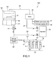
- Fig. 1 is a schematic diagram showing a configuration of a thin-film forming apparatus according to an embodiment of the present invention.
- the thin-film forming apparatus according to the embodiment allows a ferroelectric PZT thin-film to be formed using the MOCVD method.
- a thin-film forming apparatus 100 includes a raw material supply unit 10 for supplying an organic solvent solution of an organic metal, and a vaporizer 20 for vaporizing the solution to produce a raw material gas.
- the thin-film forming apparatus 100 includes a mixer 30 for producing a mixed gas by mixing a raw material gas, an oxidation gas that is reacted with the raw material and an inert gas, and a film forming chamber 50 connected to the mixer 30 via a supply line 33 as a supply path.
- the supply mechanism is configured by the raw material supply unit 10, the vaporizer 20, the mixer 30, and each line and each valve disposed thereon.
- the raw material supply unit 10 includes tanks A, B, C and D with which a raw material solution and a solvent of the organic metal is filed, and a supply line 11 for supplying He (helium) to respective tanks (A to D). Also, the raw material supply unit 10 includes a supply line 12 for supplying a carrier gas to transport the solution and the solvent of the metal raw material forced out by a pressure of He supplied to the respective tanks A to D.
- N2 nitrogen
- N2 nitrogen
- Other inert gas may be used.
- the gas supplied to the respective tanks A to D is not limited to He, and other inert gas may be used.
- the tanks A to D are filled with a Pb raw material solution, a Zr raw material solution, a Ti raw material solution and an organic solvent, respectively.
- a Pb raw material solution As the Pb, Zr and Ti raw material solutions, each metal raw material is dissolved in an n-butyl acetate solution at a concentration of 0.25 mol/L.
- Pb raw material Pb(dpm)2, (bisdipivaloyl methanate) lead is used.
- Zr raw material Zr(dmhd)4, (tetrakis(2,6)dimethyl(3,5)heptane dionate)zirconium is used.
- Ti raw material Ti(iPrO)2(dpm)2, ((bisisopropoxide)bisdipivaloyl methanate)) titanium is used.
- solvent filled in the tank D n-butyl acetate is used.
- Pb(dpm)2 is also referred to as Pb(thd)2, (bis(2,2,6,6)tetramethyl (3,5)heptanedionate) lead.
- the metal raw materials dissolved into the solvent are not limited to the above-described materials.
- the Pb raw material may include Pb(dibm)2, (bisdiisobutyryl methanate) lead, or may partly include both of Pb(dpm)2 and Pb(dibm)2 or at least one of them.
- the Zr raw material may include thd, (tetrakis(2,2,6,6)tetramethyl(3,5)heptane dionate)zirconium, or may partly include it.
- the Ti raw material may include Ti(MMP)4, (tetrakis(1)methoxy(2)methyl(2) propoxy) titanium, or may partly include it.
- toluene tetrahydrofuran (THF)
- cyclohexane ethylcyclohexane
- methylcyclohexane n-butyl acetate
- the vaporizer 20 is connected to the raw material supply unit 10 via the supply line 12, and droplets of the metal raw material solution and the solvent are transported from the raw material supply unit 10 to the vaporizer 20.
- the vaporizer 20 includes a heating means (not shown), which vaporizes the solution and the solvent of the metal raw material transported. In this way, a metal raw material gas is produced.
- a gas, ultrasonic, etc. may be applied to the droplets of the metal raw material solution and the solvent, or the droplets that have become finer via a fine nozzle in advance may be introduced.
- the vaporizer 20 includes a Run line 21 connected to the mixer 30, and a Vent line 22 connected to a vacuum evacuation system 40.
- a valve V1 is disposed in the Run line 21, and a valve V2 is disposed in the Vent line 22.
- the mixer 30 produces the mixed gas of the metal raw material gas produced by the vaporizer 20, the oxidation gas and the inert gas. Accordingly, an oxidation gas supply unit 31 and an inert gas supply unit 32 are connected to the mixer 30.
- 02 oxygen
- N2 is supplied from the inert gas supply unit 32.
- the oxidation gas dinitrogen monoxide, ozone etc. may be supplied.
- the inert gas argon etc. may be supplied.
- the film forming chamber 50 includes a chamber 51 connected to the supply line 33, and a stage 52 disposed in the chamber 51.
- a shower nozzle 53 is disposed on a ceiling plane of the chamber 51. To the shower nozzle 53, the supply line 33 is connected. The stage 52 and the shower nozzle 53 are disposed facing each other. In the chamber 51, cleaned parts such as a shield (not shown) are disposed.
- a substrate S on which the PZT thin-film is formed is placed on the stage 52.
- the stage 52 has a heating means such as a heater (not shown), and can heat the substrate S placed.
- the substrate S placed on the stage 52 is configured of an 8-inch Si substrate on which an SiO2 oxidized film is formed in a thickness of 100 nm, and Ir is formed thereon in a thickness of 70 nm by a sputtering method.
- a size, a material and the like of the substrate are not limited.
- the chamber 51 is connected to the vacuum evacuation system 40 including, for example, a dry pump, a turbo molecular pump etc. via a pressure adjusting valve 41.
- a pressure adjusting valve 41 By setting a pressure in the chamber 51 with the pressure adjusting valve 41 as appropriate, it is possible to easily accommodate a variety of film forming pressure conditions.
- Each apparatus including each line from the vaporizer 20 to the film forming chamber 50, each valve, the mixer 30 etc. is kept at a high temperature, e.g. 200°C or more, by the heating means (not shown) such that the metal raw material gas vaporized is not liquefied, for example.
- the thin-film forming apparatus 100 includes a regulating unit (not shown) as a gas supply regulating means for regulating each valve and each apparatus as described above.
- the regulating unit includes a main memory including a CPU (Central Processing Unit), a ROM (Read Only Memory) or a RAM (Random Access Memory) or the like.
- a regulating signal is output from the regulating unit to each apparatus via, for example, wired or wireless, thereby regulating operations of the thin-film forming apparatus 100.
- FIG. 2 is a schematic diagram showing a configuration of a multichamber film forming apparatus including the thin-film forming apparatus according to the embodiment.
- a multichamber film forming apparatus 200 includes a transport chamber 201 on which a transport robot (not shown) capable of transporting the substrate S is placed, and two stock chambers 202 capable of each mounting 25 substrates as a lot.
- the multichamber film forming apparatus 200 includes two thin-film forming apparatuses 100 as described above, and two film forming chambers 50 are disposed around the transport chamber 201.
- Each of the film forming chambers 50 and the stock chambers 202 is connected to the transport chamber 201 via a partition valve 203.
- the number of the stock chambers 202 is not limited to two. More stock chambers or one stock chambers may be disposed around the transport chamber 201.
- Each vacuum evacuation system 40 is connected to each film forming chamber 50.
- a vacuum evacuation system 204 is connected to each of the transport chamber 201 and the stock chambers 202.
- Each chamber can be evacuated inside independently to a vacuum atmosphere.
- one vacuum evacuation system may be simultaneously used for the transport chamber 201, the film forming chamber 50, and the stock chambers 202 to evacuate inside, for example.
- the vacuum evacuation system functions as the vacuum evacuation system 40 as shown in Fig. 1 .
- a gas source 205 is connected to the transport chamber 201. With a pressure adjusted gas such as the inert gas supplied from the gas source 205, the transport chamber 201 can be adjusted to have a predetermined pressure.
- An automatic pressure adjusting valve (not shown) disposed at the transport chamber 201 adjusts an internal pressure of the transport chamber 201.
- the stock chambers 202 are connected to a substrate transport system under atmosphere 206 via valves 203.
- the substrate transport system under atmosphere 206 includes a transport robot (not shown) for transporting the substrate S on which a film is formed or not between a plurality of wafer cassettes 207 and the stock chambers 202.
- the predetermined number of the substrate S is transported to the stock chambers 202 from the wafer cassettes 207 each including 25 wafers by the transport robot disposed on the substrate transport system under atmosphere 206.
- Each stock chamber 202 into which the substrate S is transported is vacuum evacuated.
- 1200 sccm of an adjusting gas such as N2 is supplied from the gas source 205 to the transport chamber 201 to adjust the internal pressure of the transport chamber 201.
- the internal pressure of the film forming chamber 50 is set to about 2 Torr.
- the internal pressure of the transport chamber 201 is adjusted to an almost similar pressure as the internal pressure of the film forming chamber 50 or about 5% higher than the internal pressure of the film forming chamber 50.
- the internal pressure of the film forming chamber 50 is adjusted by N2 supplied from the inert gas supply unit 32.
- the above-described film forming pressure conditions may be set as appropriate.
- the multichamber film forming apparatus 200 includes two stock chambers 202. When one stock chamber 202 is filled with the substrates S, the other stock chamber 202 can mount the substrates S. If the substrates S are mounted on the second stock chamber 202, the second stock chamber 202 is vacuum evacuated after the film forming process of the substrates S mounted on the first stock chamber 202 is ended, and the substrates S are again transported to the film forming chamber 50.
- a nozzle flush of the vaporizer 20 is started by the solvent transported by the carrier gas forced out of the tank D.
- the vaporizer 20 is prepared to vaporize the metal raw material solution and the solvent.
- the valve V2 of the Vent line 22 is opened, a vaporized gas of the solvent and the carrier gas are discarded to the Vent line 22.
- the substrate S is heated by the heating means disposed on the stage 52. Within about 3 minutes, the temperature of the substrate is stabilized at the predetermined temperature. According to the embodiment, the substrate S is heated so that the temperature of the substrate S reaches 600°C or more. The temperature of the substrate S heated may be set as appropriate.
- the vaporization by the vaporizer 20 is switched from the solvent to the subject metal raw material solution at the controlled flow rate for film forming within 2 minutes before the temperature of the substrate S is converged (the Vent line 22 keeps to be opened).
- the valve V2 of the Vent line 22 is closed and the valve V1 of the Run line 21 is opened.
- the vaporized gas of the subject metal raw material solution vaporized by the vaporizer 20 is supplied to the mixer 30.
- the vaporized gas supplied from the vaporizer 20, the oxidation gas 02 and the inert gas N2 are mixed at a predetermined mixing ratio (mol ratio).
- the mixing ratio is set as appropriate in order to provide a desirable crystalline orientation of the PZT thin-film formed, for example.
- the mixed gas produced by the mixer 30 is provided to the chamber 51 of the film forming chamber 50 via the supply line 33.
- the mixed gas is provided to the substrate S heated, and the PZT thin-film having perovskite-type crystals is formed on the substrate S.
- the PZT thin-film is formed in a thickness of about 70 nm at a film forming rate of about 15 nm/min. Accordingly, it takes about 300 seconds to form the film.
- the thickness of the PZT thin-film formed, the film forming rate, and the time for the film formation are not limited thereto.
- valve V1 of the Run line 21 is closed, and the valve V2 of the Vent line 22 is opened.
- the supply of the vaporized gas of the metal raw material solution to the substrate S in the chamber 51 is stopped, and the vaporized gas is discarded via the Vent line 22.
- the supply of 02 from the oxidation gas supply unit 31 connected to the mixer 30 is regulated.
- the "regulation" in the embodiment means that the supply of 02 to the substrate S is stopped.
- a predetermined amount of N2 is supplied from the inert gas supply unit 32, and N2 is supplied to the chamber 51 via the supply line 33 through which the mixed gas is passed.
- the amount of N2 the flow rate before the supply of 02 from the oxidation gas supply unit 31 is stopped may be retained, or the amount may be adjusted after the supply of 02 is stopped.
- the amount of N2 may be set so that the internal pressure of the chamber 51 satisfies the film forming pressure conditions (about 2 Torr).
- the partition valve 203 between the film forming chamber 50 and the transport chamber 201 is opened, and the substrate S film formed is unloaded.
- the substrate S is unloaded after about 60 seconds elapsed, but is not limited thereto.
- the substrate S may be unloaded after 30 seconds to 120 seconds elapsed.
- a time took for unloading the substrate S may be set as appropriate depending on the time for the film formation and a possibility of changes in the substrate.
- the substrate S is unloaded.
- the substrate S can be unloaded after the mixed gas remained in the film forming chamber 50 is sufficiently evacuated. This can prevent the mixed gas remained from flowing into the transport chamber 201 and particles etc. from generating, when the substrate S is unloaded.
- Fig. 3 is graphs each showing a Pb composition ratio, film (Pb/(Zr + Ti)), and a Zr composition ratio, film(Zr/(Zr + Ti)) in the PZT thin-film formed to the flow rate ratio of the Pb raw material gas supplied to a substrate S.
- Fig. 3 shows the graph of the PZT thin-film formed by the thin-film forming apparatus 100 according to the embodiment, and the graph of the PZT thin-film formed by a comparative thin-film forming method.
- the PZT thin-film according to the embodiment is formed by supplying N2 to the chamber 51 after the film formation, i.e., subsequent to the stop of the supply of the metal raw material gas to the film forming chamber 50.
- the comparative PZT thin-film is formed by supplying 02 to the chamber 51 after stopping the supply of the metal raw material gas to the film forming chamber 50.
- the PZT thin-film that is the dielectric thin-film including the perovskite type crystals is formed, another phase region, the self-alignment region and a PbO precipitated region are emerged in this order from a small flow rate of the Pb raw material gas.
- the Pb composition is less than stoichiometric and a crystalline PZT thin-film will not be provided.
- the self-alignment region the Pb composition ratio in the thin-film is less changed even if the flow rate of the Pb raw material gas is changed.
- the PbO precipitated region PbO crystals are precipitated and the Pb composition in the thin-film is rapidly increased.
- Fig. 3 shows the graphs of measurement results of the self-alignment region among the three regions.
- the region where the Pb flow rate ratio value is from about 1.15 to about 1.5 is identified as the self-alignment region.
- the self-alignment region is changed based on respective film forming conditions such as the internal pressure of the film forming chamber 50 and the temperature, for example. Therefore, when the PZT thin-film is formed, the Pb flow rate ratio included in the self-alignment region is set as appropriate based on the respective film forming conditions.
- the Zr composition ratio in the PZT thin-film can be set as appropriate based on the Zr flow rate ratio in the raw material supply unit 10 as shown in Fig. 1 .
- the Zr composition ratio may be set such that the PZT thin-film formed has desirable properties.
- the comparative PZT thin-film formed has the Pb composition ratio greater than that of the PZT thin-film formed according to the embodiment.
- an increase of the Pb composition in the self-alignment region can be inhibited in the film formed by the method according to the embodiment using N2 as the supplied gas after the film forming as compared with the film formed by the comparative method using O2 as the supplied gas after the film formation.
- the PZT crystals are ideally provided, and extra atoms not constituting the perovskite type crystals are excluded.
- excess Pb atoms actually remain, for example, on the surface or crystal grain boundaries of the PZT thin-film.
- Pb may be attached to parts etc. of the chamber 51.
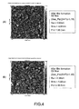
- Fig. 4 shows photographs of respective surface layers of the PZT thin-film formed by the thin-film forming apparatus shown 100 according to the embodiment and the PZT thin-film formed by the comparative method, and respective measured values of the surface layers.
- Fig. 4(A) shows the PZT thin-film according to the embodiment
- Fig. 4 (B) shows the comparative PZT thin-film. Respective photographs are captured by an atomic force microscope.
- Respective PZT thin-films shown in Figs. 4(A) and (B) are formed when the flow rate ratio of the Pb raw material gas is 1.15.
- the measured value Ra is an average surface roughness
- the measured value Rms is a square average roughness.
- the measured value P-V is a peak-to-valley.
- the film formation method according to the embodiment can inhibit the extra Pb atoms not constituting the perovskite type crystals from introducing into the surface layer of the PZT thin-film as PbO after the film formation. This is because the surface roughness of the PZT thin-film according to the embodiment becomes smaller.
- the thin-film forming apparatus 100 As described above, in the thin-film forming apparatus 100 according to the embodiment and the thin-film forming method by the apparatus 100, after the supply of the metal raw material gas to the substrate S is stopped, the supply of 02 to the substrate S is stopped. Thus, it can be inhibited from reacting extra Pb atoms not constituting the perovskite type crystals with 02. In this way, the extra Pb atoms will not be introduced into the surface layer of the PZT thin-film, for example, as the oxide PbO, and the PZT thin-film having a small surface roughness can be formed.
- the inert gas N2 is supplied to the chamber 51.
- This allows the internal pressure of the chamber 51 to be adjusted to satisfy the film forming pressure conditions, for example. In this way, the film forming process can be effectively carried out, when the PZT thin-films are sequentially formed on a plurality, e.g., about 300, of substrates S.
- the inert gas supply unit 32 is connected to the mixer 30, as shown in Fig. 1 .
- the mixed gas for forming the PZT thin-film contains the inert gas N2.
- the N2 is supplied to the chamber 51 in response to the stop of the 02 supply. In this way, a new mechanism for supplying the inert gas to the chamber 51 after the film formation becomes unnecessary, thereby easily supplying the inert gas after the film formation.
- the mixed gas is supplied via the supply line 33 that connects the mixer 30 with the chamber 51.
- N2 is supplied via the supply line 33 through which the mixed gas is passed.
- the mixed gas containing the metal raw material gas is forced to supply N2 to the chamber 51.
- the metal raw material gas (the mixed gas) accumulated at the supply line is prevented from supplying to the chamber 51 during the N2 is supplied after the film formation, and the PZT thin-film can be stably formed on the substrate S.
- Fig. 5 is a schematic diagram showing a modification of the thin-film forming apparatus 100 shown in Fig. 1 .
- an inert gas supply unit 332 is not connected to a mixer 330, and is separately connected to a shower nozzle 353 of a chamber 351.
- the metal raw material gas is mixed with the oxidation gas.
- the mixed gas is supplied to the substrate S.
- the PZT thin-film is formed on the substrate S.
- the supply of the mixed gas (the metal raw material gas and the oxidation gas) from the mixer 330 is stopped, and the inert gas is supplied to the chamber from the inert gas supply unit 332.
- the inert gas supply unit 332 may be connected to the chamber 351 separately from the mixer 330.
- the inert gas After stopping the supply of the metal raw material gas to the substrate, the inert gas may not be supplied. Even in this case, when the supply of the oxidation gas is stopped after stopping the supply of the metal raw material gas, it can prevent unnecessary Pb atoms from reacting with the oxidation gas after the film formation, and the oxide PbO from introducing into the surface layer of the PZT thin-film. Even if the inert gas is not supplied after the film formation, the oxidation gas is virtually evacuated from the inside of the film forming chamber after the film formation. Under this state, the substrate is transported from the transport chamber.
- the mixer may not be disposed, and the metal raw material gas, the oxidation gas supply unit and the inert gas supply unit may be individually connected to the chamber.
- the mixed gas of the metal raw material gas, the oxidation gas and the inert gas will be produced in the chamber.
- the supply of the oxidation gas and the inert gas may be regulated as described above.
- the supply of the oxidation gas after stopping the supply of the metal raw material gas to the substrate, the supply of the oxidation gas is stopped.
- the supply of the oxidation gas may be decreased after the film formation.
- the regulation of the supply of the oxidation gas may include both of the stop and the decrease of the supply of the oxidation gas.
- the PZT thin-film is formed using the thin-film forming apparatus 100.
- the present invention is applicable to the formation of the thin-film other than the PZT thin-film formed as the dielectric thin-film having a perovskite structure.
- examples include the dielectric thin-film of lanthanum-doped lead zirconate titanate ((Pb, La)(Zr, Ti)O3; PLZT), strontium bismuth tantalite (SrBi2, Ta2, 09; SBT) and the like.
- the multichamber film forming apparatus 200 is illustrated above, as shown in Fig. 2 .
- the thin-film forming apparatus 100 of the embodiment may be disposed on a substrate processing apparatus including a plurality of process apparatuses such as an etching process apparatus and a cleaning process apparatus.
- the substrate process apparatus include a cluster tool type substrate process apparatus and an in-line type substrate process apparatus.
Landscapes
- Chemical & Material Sciences (AREA)
- Organic Chemistry (AREA)
- General Chemical & Material Sciences (AREA)
- Chemical Kinetics & Catalysis (AREA)
- Engineering & Computer Science (AREA)
- Materials Engineering (AREA)
- Mechanical Engineering (AREA)
- Metallurgy (AREA)
- Inorganic Chemistry (AREA)
- Formation Of Insulating Films (AREA)
- Semiconductor Memories (AREA)
- Chemical Vapour Deposition (AREA)
Abstract
Description
- The present invention relates to a method of forming a dielectric thin-film such as a PZT (lead zirconate titanate) thin-film, and a thin-film forming apparatus.
- In the related art, as a ferroelectric thin-film for use in a ferroelectric random access memory (FeRAM) or the like, a thin-film of lead zirconate titanate (Pb(Zr,Ti)O3; PZT) having a perovskite structure is known. Such dielectric thin-film is formed by a Metal Organic Chemical Vapor Deposition (MOCVD) method.
- The MOCVD method is a method of forming the dielectric thin-film by reacting a raw material organic metal gas with an oxidation gas at a high temperature. In order to form the dielectric thin-film with a high quality, it uses a self-alignment region where a composition ratio of the thin-film is less changed even if a flow rate of the raw material gas is changed.
-
Patent Document 1 describes a MOCVD method of supplying a mixed gas of an organic metal raw material gas, an oxidation gas and a diluent gas to a substrate that has been heated. In the MOCVD method described inPatent Document 1, a combustible gas is also supplied when the mixed gas is supplied to the substrate. As excess oxygen on the surface of the substrate is combusted and discharged, a high quality thin-film can be formed (see paragraphs [0011] and [0025] inPatent Document 1. - Patent Document 1: Japanese Patent Application Laid-open No.
2004-273787 - When the dielectric thin-film is formed as described above, the dielectric thin-film preferably has a small surface roughness. If the dielectric thin-film has a high surface roughness, the process of forming a ferroelectric memory having, for example, the dielectric thin-film may cause a problem. Also, there is a concern about that electrical properties of the dielectric thin-film are not sufficiently provided, for example.
- In view of the circumstances as described above, an object of the present invention is to provide a thin-film forming method and a thin-film forming apparatus, both of which enable the formation of a dielectric thin-film having a small surface roughness.
- In order to achieve the above-mentioned object, a method of forming a thin-film according to an embodiment of the present invention comprises supplying a mixed gas to a substrate that is placed and heated in a chamber; the mixed gas containing a metal raw material gas that serves as a raw material for a dielectric thin-film having perovskite type crystals and an oxidation gas that is reacted with the metal raw material gas.
The supply of the metal raw material gas to the substrate is stopped.
After stopping the supply of the metal raw material gas, the supply of the oxidation gas to the substrate is regulated. - A thin-film forming apparatus according to an embodiment of the present invention comprises a chamber, a supply mechanism and a gas supply regulating means.
In the chamber, a heated substrate is placed.
The supply mechanism is to supply the substrate heated and placed in the chamber with a mixed gas of a metal raw material gas that serves as a raw material of a dielectric thin-film having a perovskite structure and an oxidation gas that is reacted with the metal raw material gas.
The gas supply regulating means is for stopping the supply of the metal raw material gas to the substrate, and then regulating the supply of the oxidation gas to the substrate. -
- [
Fig. 1 ] A schematic diagram showing a configuration of a thin-film forming apparatus according to an embodiment of the present invention. - [
Fig. 2 ] A schematic diagram showing a configuration of a multichamber film forming apparatus including the thin-film forming apparatus shown inFig. 1 . - [
Fig. 3 ] Graphs each showing a Pb composition ratio and a Zr composition ratio in a PZT thin-film formed to a flow rate ratio of a Pb raw material gas supplied to a substrate. - [
Fig. 4 ] Photographs of respective surface layers of a PZT thin-film formed by the thin-film forming apparatus shown inFig. 1 and a PZT thin-film formed by a comparative forming method; and respective measured values of the surface layers. - [
Fig. 5 ] A schematic diagram showing a modification of the thin-film forming apparatus shown inFig. 1 . Mode(s) for Carrying Out the Invention - A method of forming a thin-film according to an embodiment of the present invention includes supplying a heated substrate in a chamber with a mixed gas of a metal raw material gas of a dielectric thin-film including perovskite type crystals and an oxidation gas that is reacted with the metal raw material gas.
The supply of the metal raw material gas to the substrate is stopped.
After stopping the supply of the metal raw material gas, the supply of the oxidation gas to the substrate is regulated. - According to the method of forming a thin-film, it can be inhibited from reacting extra atoms not constituting the perovskite type crystals with the oxidation gas, after stopping the supply of the metal raw material gas. In this way, the extra atoms will not be introduced into a surface layer of the dielectric thin-film, for example, as an oxide, and the dielectric thin-film having a small surface roughness can be formed.
- In the regulating step, the supply of the oxidation gas may be stopped or decreased. In this case, the method of forming a thin-film may further include supplying an inert gas to the chamber in response to the stop or the decrease of the oxidation gas supply.
- According to the method of forming a thin-film, in response to the stop or the decrease of the oxidation gas supply, the inert gas is supplied to the chamber. The inert gas allows a pressure in the chamber to be adjusted, for example. In this way, a film forming process can be effectively carried out, when dielectric thin-films are sequentially formed on a plurality of substrates.
- In the step of supplying the mixed gas, the mixed gas containing the inert gas may be supplied. In this case, in the step of supplying the inert gas in response to the stop or the decrease of the oxidation gas supply, the inert gas contained in the mixed gas may be supplied.
- According to the method of forming a thin-film, the mixed gas for use in the formation of the dielectric thin-film contains the inert gas. The inert gas is supplied to the chamber in response to the stop or the decrease of the oxidation gas supply. In this way, a new mechanism for supplying the inert gas becomes unnecessary, thereby easily supplying the inert gas.
- In the step of supplying the mixed gas, the mixed gas may be supplied via a supply path that connects a mixer for mixing the metal raw material gas, the oxidation gas and the inert gas to the chamber. In this case, the step of supplying the inert gas may supply the inert gas via the supply path through which the mixed gas is passed.
- According to the method of forming a thin-film, the inert gas is supplied to the chamber via the supply path through which the mixed gas is passed. In this way, it can prevent the mixed gas from accumulating at the supply path. As a result, the dielectric thin-film can be stably formed on the substrate.
- The dielectric thin-film may be PZT (Pb(Zr, Ti)O3). In this case, the metal raw material may contain a material partly including Pb(dpm)2 and Pb(dibm)2 or at least one of them.
- The substrate may be heated at 600°C or more.
- A thin-film forming apparatus according to an embodiment of the present invention includes a chamber, a supply mechanism and a gas supply regulating means.
A heated substrate is placed in the chamber.
The supply mechanism is for supplying the heated substrate in the chamber with a mixed gas of a metal raw material gas that serves as a raw material of a dielectric thin-film having a perovskite structure and an oxidation gas that is reacted with the metal raw material gas.
The gas supply regulating means stops the supply of the metal raw material gas to the substrate, and regulates the supply of the oxidation gas to the substrate. - Hereinafter, embodiments according to the present invention will be described with reference to the drawings.
-
Fig. 1 is a schematic diagram showing a configuration of a thin-film forming apparatus according to an embodiment of the present invention. The thin-film forming apparatus according to the embodiment allows a ferroelectric PZT thin-film to be formed using the MOCVD method. - A thin-
film forming apparatus 100 includes a rawmaterial supply unit 10 for supplying an organic solvent solution of an organic metal, and avaporizer 20 for vaporizing the solution to produce a raw material gas. The thin-film forming apparatus 100 includes amixer 30 for producing a mixed gas by mixing a raw material gas, an oxidation gas that is reacted with the raw material and an inert gas, and afilm forming chamber 50 connected to themixer 30 via a supply line 33 as a supply path. According to the embodiment, the supply mechanism is configured by the rawmaterial supply unit 10, thevaporizer 20, themixer 30, and each line and each valve disposed thereon. - The raw
material supply unit 10 includes tanks A, B, C and D with which a raw material solution and a solvent of the organic metal is filed, and asupply line 11 for supplying He (helium) to respective tanks (A to D). Also, the rawmaterial supply unit 10 includes asupply line 12 for supplying a carrier gas to transport the solution and the solvent of the metal raw material forced out by a pressure of He supplied to the respective tanks A to D. In the embodiment, N2 (nitrogen) is used as a carrier gas, but is not limited thereto. Other inert gas may be used. In the same manner, the gas supplied to the respective tanks A to D is not limited to He, and other inert gas may be used. - In the embodiment, the tanks A to D are filled with a Pb raw material solution, a Zr raw material solution, a Ti raw material solution and an organic solvent, respectively. As the Pb, Zr and Ti raw material solutions, each metal raw material is dissolved in an n-butyl acetate solution at a concentration of 0.25 mol/L.
- As the Pb raw material, Pb(dpm)2, (bisdipivaloyl methanate) lead is used. As the Zr raw material, Zr(dmhd)4, (tetrakis(2,6)dimethyl(3,5)heptane dionate)zirconium is used. As the Ti raw material, Ti(iPrO)2(dpm)2, ((bisisopropoxide)bisdipivaloyl methanate)) titanium is used. As the solvent filled in the tank D, n-butyl acetate is used. Pb(dpm)2 is also referred to as Pb(thd)2, (bis(2,2,6,6)tetramethyl (3,5)heptanedionate) lead.
- The metal raw materials dissolved into the solvent are not limited to the above-described materials. For example, the Pb raw material may include Pb(dibm)2, (bisdiisobutyryl methanate) lead, or may partly include both of Pb(dpm)2 and Pb(dibm)2 or at least one of them. The Zr raw material may include thd, (tetrakis(2,2,6,6)tetramethyl(3,5)heptane dionate)zirconium, or may partly include it. The Ti raw material may include Ti(MMP)4, (tetrakis(1)methoxy(2)methyl(2) propoxy) titanium, or may partly include it.
- As the solvent for dissolving each metal raw material and a solvent filled in the tank D, toluene, tetrahydrofuran (THF), cyclohexane, ethylcyclohexane, methylcyclohexane or the like may be used instead of n-butyl acetate as described above.
- The
vaporizer 20 is connected to the rawmaterial supply unit 10 via thesupply line 12, and droplets of the metal raw material solution and the solvent are transported from the rawmaterial supply unit 10 to thevaporizer 20. Thevaporizer 20 includes a heating means (not shown), which vaporizes the solution and the solvent of the metal raw material transported. In this way, a metal raw material gas is produced. In order to improve vaporization efficiency, a gas, ultrasonic, etc. may be applied to the droplets of the metal raw material solution and the solvent, or the droplets that have become finer via a fine nozzle in advance may be introduced. - As shown in
Fig. 1 , thevaporizer 20 includes aRun line 21 connected to themixer 30, and aVent line 22 connected to avacuum evacuation system 40. A valve V1 is disposed in theRun line 21, and a valve V2 is disposed in theVent line 22. - The
mixer 30 produces the mixed gas of the metal raw material gas produced by thevaporizer 20, the oxidation gas and the inert gas. Accordingly, an oxidationgas supply unit 31 and an inertgas supply unit 32 are connected to themixer 30. In the embodiment, 02 (oxygen) is supplied from the oxidationgas supply unit 31, and N2 is supplied from the inertgas supply unit 32. However, as the oxidation gas, dinitrogen monoxide, ozone etc. may be supplied. Also, as the inert gas, argon etc. may be supplied. - The
film forming chamber 50 includes achamber 51 connected to the supply line 33, and astage 52 disposed in thechamber 51. Ashower nozzle 53 is disposed on a ceiling plane of thechamber 51. To theshower nozzle 53, the supply line 33 is connected. Thestage 52 and theshower nozzle 53 are disposed facing each other. In thechamber 51, cleaned parts such as a shield (not shown) are disposed. - As shown in
Fig. 1 , on thestage 52, a substrate S on which the PZT thin-film is formed is placed. Thestage 52 has a heating means such as a heater (not shown), and can heat the substrate S placed. In the embodiment, the substrate S placed on thestage 52 is configured of an 8-inch Si substrate on which an SiO2 oxidized film is formed in a thickness of 100 nm, and Ir is formed thereon in a thickness of 70 nm by a sputtering method. However, a size, a material and the like of the substrate are not limited. - The
chamber 51 is connected to thevacuum evacuation system 40 including, for example, a dry pump, a turbo molecular pump etc. via apressure adjusting valve 41. By setting a pressure in thechamber 51 with thepressure adjusting valve 41 as appropriate, it is possible to easily accommodate a variety of film forming pressure conditions. - Each apparatus including each line from the
vaporizer 20 to thefilm forming chamber 50, each valve, themixer 30 etc. is kept at a high temperature, e.g. 200°C or more, by the heating means (not shown) such that the metal raw material gas vaporized is not liquefied, for example. - The thin-
film forming apparatus 100 according to the embodiment includes a regulating unit (not shown) as a gas supply regulating means for regulating each valve and each apparatus as described above. The regulating unit includes a main memory including a CPU (Central Processing Unit), a ROM (Read Only Memory) or a RAM (Random Access Memory) or the like. A regulating signal is output from the regulating unit to each apparatus via, for example, wired or wireless, thereby regulating operations of the thin-film forming apparatus 100. -
Fig. 2 is a schematic diagram showing a configuration of a multichamber film forming apparatus including the thin-film forming apparatus according to the embodiment. A multichamberfilm forming apparatus 200 includes atransport chamber 201 on which a transport robot (not shown) capable of transporting the substrate S is placed, and twostock chambers 202 capable of each mounting 25 substrates as a lot. The multichamberfilm forming apparatus 200 includes two thin-film forming apparatuses 100 as described above, and twofilm forming chambers 50 are disposed around thetransport chamber 201. Each of thefilm forming chambers 50 and thestock chambers 202 is connected to thetransport chamber 201 via apartition valve 203. The number of thestock chambers 202 is not limited to two. More stock chambers or one stock chambers may be disposed around thetransport chamber 201. - Each
vacuum evacuation system 40 is connected to eachfilm forming chamber 50. Similarly, avacuum evacuation system 204 is connected to each of thetransport chamber 201 and thestock chambers 202. Each chamber can be evacuated inside independently to a vacuum atmosphere. Alternatively, one vacuum evacuation system may be simultaneously used for thetransport chamber 201, thefilm forming chamber 50, and thestock chambers 202 to evacuate inside, for example. In this case, the vacuum evacuation system functions as thevacuum evacuation system 40 as shown inFig. 1 . - A gas source 205 is connected to the
transport chamber 201. With a pressure adjusted gas such as the inert gas supplied from the gas source 205, thetransport chamber 201 can be adjusted to have a predetermined pressure. An automatic pressure adjusting valve (not shown) disposed at thetransport chamber 201 adjusts an internal pressure of thetransport chamber 201. - As shown in
Fig. 2 , thestock chambers 202 are connected to a substrate transport system underatmosphere 206 viavalves 203. The substrate transport system underatmosphere 206 includes a transport robot (not shown) for transporting the substrate S on which a film is formed or not between a plurality ofwafer cassettes 207 and thestock chambers 202. - When the film forming step is started, the predetermined number of the substrate S is transported to the
stock chambers 202 from thewafer cassettes 207 each including 25 wafers by the transport robot disposed on the substrate transport system underatmosphere 206. Eachstock chamber 202 into which the substrate S is transported is vacuum evacuated. - Each
valve 203 disposed between eachstock chamber 202 vacuum evacuated and thetransport chamber 201 is opened, and both of thetransport chamber 201 and eachstock chamber 202 are then vacuum evacuated. 1200 sccm of an adjusting gas such as N2 is supplied from the gas source 205 to thetransport chamber 201 to adjust the internal pressure of thetransport chamber 201. - In the embodiment, as the film forming pressure conditions, the internal pressure of the
film forming chamber 50 is set to about 2 Torr. Correspondingly, the internal pressure of thetransport chamber 201 is adjusted to an almost similar pressure as the internal pressure of thefilm forming chamber 50 or about 5% higher than the internal pressure of thefilm forming chamber 50. The internal pressure of thefilm forming chamber 50 is adjusted by N2 supplied from the inertgas supply unit 32. The above-described film forming pressure conditions may be set as appropriate. After the pressure adjustment of thetransport chamber 201 is almost ended, the first substrate S is transported to the film forming chamber 501 via thetransport chamber 201. - The multichamber
film forming apparatus 200 according to the embodiment includes twostock chambers 202. When onestock chamber 202 is filled with the substrates S, theother stock chamber 202 can mount the substrates S. If the substrates S are mounted on thesecond stock chamber 202, thesecond stock chamber 202 is vacuum evacuated after the film forming process of the substrates S mounted on thefirst stock chamber 202 is ended, and the substrates S are again transported to thefilm forming chamber 50. - When He is supplied from the
supply line 11 for supplying He to each of the tanks A to D as shown inFig. 1 , the internal pressure of each of the tanks A to D increases, whereby the raw material solution and the solvent of the organic metal filled in each of the tanks A to D are forced out to thesupply line 12 for supplying the carrier gas (N2). The forced droplets of the metal raw material solution and the solvent are regulated for the flow rate by a liquid flow rate regulator or the like, and are transported to thevaporizer 20 by the carrier gas. - Once the film forming step is started, a nozzle flush of the
vaporizer 20 is started by the solvent transported by the carrier gas forced out of the tank D. Within about 3 minutes, thevaporizer 20 is prepared to vaporize the metal raw material solution and the solvent. In this case, the valve V2 of theVent line 22 is opened, a vaporized gas of the solvent and the carrier gas are discarded to theVent line 22. - When the first substrate S is transported to the
film forming chamber 50 and is mounted on thestage 52, the substrate S is heated by the heating means disposed on thestage 52. Within about 3 minutes, the temperature of the substrate is stabilized at the predetermined temperature. According to the embodiment, the substrate S is heated so that the temperature of the substrate S reaches 600°C or more. The temperature of the substrate S heated may be set as appropriate. - The vaporization by the
vaporizer 20 is switched from the solvent to the subject metal raw material solution at the controlled flow rate for film forming within 2 minutes before the temperature of the substrate S is converged (theVent line 22 keeps to be opened). - Once the temperature of the substrate S or a part such as the
shower nozzle 53 reaches the predetermined temperature, the valve V2 of theVent line 22 is closed and the valve V1 of theRun line 21 is opened. The vaporized gas of the subject metal raw material solution vaporized by thevaporizer 20 is supplied to themixer 30. - In the
mixer 30, the vaporized gas supplied from thevaporizer 20, theoxidation gas 02 and the inert gas N2 are mixed at a predetermined mixing ratio (mol ratio). The mixing ratio is set as appropriate in order to provide a desirable crystalline orientation of the PZT thin-film formed, for example. - The mixed gas produced by the
mixer 30 is provided to thechamber 51 of thefilm forming chamber 50 via the supply line 33. The mixed gas is provided to the substrate S heated, and the PZT thin-film having perovskite-type crystals is formed on the substrate S. In the embodiment, the PZT thin-film is formed in a thickness of about 70 nm at a film forming rate of about 15 nm/min. Accordingly, it takes about 300 seconds to form the film. However, the thickness of the PZT thin-film formed, the film forming rate, and the time for the film formation are not limited thereto. - After the film formation, the valve V1 of the
Run line 21 is closed, and the valve V2 of theVent line 22 is opened. Thus, the supply of the vaporized gas of the metal raw material solution to the substrate S in thechamber 51 is stopped, and the vaporized gas is discarded via theVent line 22. - In the embodiment, after the supply of the metal raw material gas to the substrate S is stopped, the supply of 02 from the oxidation
gas supply unit 31 connected to themixer 30 is regulated. The "regulation" in the embodiment means that the supply of 02 to the substrate S is stopped. Then, a predetermined amount of N2 is supplied from the inertgas supply unit 32, and N2 is supplied to thechamber 51 via the supply line 33 through which the mixed gas is passed. As the amount of N2, the flow rate before the supply of 02 from the oxidationgas supply unit 31 is stopped may be retained, or the amount may be adjusted after the supply of 02 is stopped. Alternatively, the amount of N2 may be set so that the internal pressure of thechamber 51 satisfies the film forming pressure conditions (about 2 Torr). - After a given time elapses from the stop of the supply of the vaporized gas of the metal raw material solution to the
chamber 51 and the supply of a predetermined amount of N2 to thechamber 51, thepartition valve 203 between thefilm forming chamber 50 and thetransport chamber 201 is opened, and the substrate S film formed is unloaded. According to the embodiment, the substrate S is unloaded after about 60 seconds elapsed, but is not limited thereto. For example, the substrate S may be unloaded after 30 seconds to 120 seconds elapsed. A time took for unloading the substrate S may be set as appropriate depending on the time for the film formation and a possibility of changes in the substrate. - As described above, after a given time elapses from N2 is supplied after the film is formed, the substrate S is unloaded. Thus, the substrate S can be unloaded after the mixed gas remained in the
film forming chamber 50 is sufficiently evacuated. This can prevent the mixed gas remained from flowing into thetransport chamber 201 and particles etc. from generating, when the substrate S is unloaded. -
Fig. 3 is graphs each showing a Pb composition ratio, film (Pb/(Zr + Ti)), and a Zr composition ratio, film(Zr/(Zr + Ti)) in the PZT thin-film formed to the flow rate ratio of the Pb raw material gas supplied to a substrate S. -
Fig. 3 shows the graph of the PZT thin-film formed by the thin-film forming apparatus 100 according to the embodiment, and the graph of the PZT thin-film formed by a comparative thin-film forming method. The PZT thin-film according to the embodiment is formed by supplying N2 to thechamber 51 after the film formation, i.e., subsequent to the stop of the supply of the metal raw material gas to thefilm forming chamber 50. On the other hand, the comparative PZT thin-film is formed by supplying 02 to thechamber 51 after stopping the supply of the metal raw material gas to thefilm forming chamber 50. - When the PZT thin-film that is the dielectric thin-film including the perovskite type crystals is formed, another phase region, the self-alignment region and a PbO precipitated region are emerged in this order from a small flow rate of the Pb raw material gas. In the another phase region, the Pb composition is less than stoichiometric and a crystalline PZT thin-film will not be provided. In the self-alignment region, the Pb composition ratio in the thin-film is less changed even if the flow rate of the Pb raw material gas is changed. In the PbO precipitated region, PbO crystals are precipitated and the Pb composition in the thin-film is rapidly increased.
Fig. 3 shows the graphs of measurement results of the self-alignment region among the three regions. - In
Fig. 3 , the region where the Pb flow rate ratio value is from about 1.15 to about 1.5 is identified as the self-alignment region. However, the self-alignment region is changed based on respective film forming conditions such as the internal pressure of thefilm forming chamber 50 and the temperature, for example. Therefore, when the PZT thin-film is formed, the Pb flow rate ratio included in the self-alignment region is set as appropriate based on the respective film forming conditions. - As shown in
Fig. 3 , there is almost no difference as to the Zr composition ratio in the PZT thin-film generated between the PZT thin-film according to the embodiment and the comparative PZT thin-film. In other words, there is almost no change in the Zr composition ratio in the PZT thin-film regardless of using N2 or O2 as the gas supplied to thechamber 51 after the film formation. The Zr composition ratio in the PZT thin-film can be set as appropriate based on the Zr flow rate ratio in the rawmaterial supply unit 10 as shown inFig. 1 . The Zr composition ratio may be set such that the PZT thin-film formed has desirable properties. - On the other hand, the comparative PZT thin-film formed has the Pb composition ratio greater than that of the PZT thin-film formed according to the embodiment. In other words, an increase of the Pb composition in the self-alignment region can be inhibited in the film formed by the method according to the embodiment using N2 as the supplied gas after the film forming as compared with the film formed by the comparative method using O2 as the supplied gas after the film formation.
- By the mechanism in the self-alignment region, the PZT crystals are ideally provided, and extra atoms not constituting the perovskite type crystals are excluded. However, excess Pb atoms actually remain, for example, on the surface or crystal grain boundaries of the PZT thin-film. Also, Pb may be attached to parts etc. of the
chamber 51. - It is considered that excess Pb atoms remained in the PZT thin-film and Pb atoms volatilized from the PZT thin-film are bonded to 02 on the substrate heated at 600°C or more to easily produce PbO, when 02 is supplied after the film formation under the circumstances. It is also considered that Pb atoms in a gas phase volatilized from Pb attached to the parts in the
chamber 51 are bonded to 02. The produced PbO is introduced into the crystal grain boundaries and the surface layer of the PZT thin-film. It is thus considered that the results shown in the graphs ofFig. 3 are provided. -
Fig. 4 shows photographs of respective surface layers of the PZT thin-film formed by the thin-film forming apparatus shown 100 according to the embodiment and the PZT thin-film formed by the comparative method, and respective measured values of the surface layers.Fig. 4(A) shows the PZT thin-film according to the embodiment, andFig. 4 (B) shows the comparative PZT thin-film. Respective photographs are captured by an atomic force microscope. - Respective PZT thin-films shown in
Figs. 4(A) and (B) are formed when the flow rate ratio of the Pb raw material gas is 1.15. The measured value Ra is an average surface roughness, and the measured value Rms is a square average roughness. The measured value P-V is a peak-to-valley. - These measured values reveal that the surface roughness of the PZT thin-film formed by the thin-
film forming apparatus 100 according to the embodiment is smaller than that of the PZT thin-film formed by the comparative method. As described above, the film formation method according to the embodiment can inhibit the extra Pb atoms not constituting the perovskite type crystals from introducing into the surface layer of the PZT thin-film as PbO after the film formation. This is because the surface roughness of the PZT thin-film according to the embodiment becomes smaller. - As described above, in the thin-
film forming apparatus 100 according to the embodiment and the thin-film forming method by theapparatus 100, after the supply of the metal raw material gas to the substrate S is stopped, the supply of 02 to the substrate S is stopped. Thus, it can be inhibited from reacting extra Pb atoms not constituting the perovskite type crystals with 02. In this way, the extra Pb atoms will not be introduced into the surface layer of the PZT thin-film, for example, as the oxide PbO, and the PZT thin-film having a small surface roughness can be formed. - In the method of forming a thin-film according to the embodiment, in response to the stop of the 02 supply after the film formation, the inert gas N2 is supplied to the
chamber 51. This allows the internal pressure of thechamber 51 to be adjusted to satisfy the film forming pressure conditions, for example. In this way, the film forming process can be effectively carried out, when the PZT thin-films are sequentially formed on a plurality, e.g., about 300, of substrates S. - In the method of forming a thin-film according to the embodiment, the inert
gas supply unit 32 is connected to themixer 30, as shown inFig. 1 . The mixed gas for forming the PZT thin-film contains the inert gas N2. The N2 is supplied to thechamber 51 in response to the stop of the 02 supply. In this way, a new mechanism for supplying the inert gas to thechamber 51 after the film formation becomes unnecessary, thereby easily supplying the inert gas after the film formation. - In the method of forming a thin-film according to the embodiment, the mixed gas is supplied via the supply line 33 that connects the
mixer 30 with thechamber 51. After the film formation, N2 is supplied via the supply line 33 through which the mixed gas is passed. Thus, after stopping the supply of the metal raw material gas, the mixed gas containing the metal raw material gas is forced to supply N2 to thechamber 51. In this way, it can prevent the metal raw material gas from accumulating at the supply line 33. As a result, the metal raw material gas (the mixed gas) accumulated at the supply line is prevented from supplying to thechamber 51 during the N2 is supplied after the film formation, and the PZT thin-film can be stably formed on the substrate S. - The present invention is not limited to the above-described embodiments, and variations and modifications may be made without departing from the scope of the present invention.
- For example,
Fig. 5 is a schematic diagram showing a modification of the thin-film forming apparatus 100 shown inFig. 1 . In a thin-film forming apparatus 300, an inertgas supply unit 332 is not connected to amixer 330, and is separately connected to ashower nozzle 353 of achamber 351. In themixer 330, the metal raw material gas is mixed with the oxidation gas. The mixed gas is supplied to the substrate S. In this way, the PZT thin-film is formed on the substrate S. After the film formation, the supply of the mixed gas (the metal raw material gas and the oxidation gas) from themixer 330 is stopped, and the inert gas is supplied to the chamber from the inertgas supply unit 332. Thus, the inertgas supply unit 332 may be connected to thechamber 351 separately from themixer 330. - After stopping the supply of the metal raw material gas to the substrate, the inert gas may not be supplied. Even in this case, when the supply of the oxidation gas is stopped after stopping the supply of the metal raw material gas, it can prevent unnecessary Pb atoms from reacting with the oxidation gas after the film formation, and the oxide PbO from introducing into the surface layer of the PZT thin-film. Even if the inert gas is not supplied after the film formation, the oxidation gas is virtually evacuated from the inside of the film forming chamber after the film formation. Under this state, the substrate is transported from the transport chamber.
- Alternatively, the mixer may not be disposed, and the metal raw material gas, the oxidation gas supply unit and the inert gas supply unit may be individually connected to the chamber. In this case, the mixed gas of the metal raw material gas, the oxidation gas and the inert gas will be produced in the chamber. After the film formation, the supply of the oxidation gas and the inert gas may be regulated as described above.
- In the above-described embodiment, after stopping the supply of the metal raw material gas to the substrate, the supply of the oxidation gas is stopped. However, the supply of the oxidation gas may be decreased after the film formation. In other words, the regulation of the supply of the oxidation gas may include both of the stop and the decrease of the supply of the oxidation gas. By decreasing the supply of the oxidation gas after the film formation, it can be inhibited from reacting extra Pb atoms with the oxidation gas.
- According to the above-described embodiment, the PZT thin-film is formed using the thin-
film forming apparatus 100. However, the present invention is applicable to the formation of the thin-film other than the PZT thin-film formed as the dielectric thin-film having a perovskite structure. Examples include the dielectric thin-film of lanthanum-doped lead zirconate titanate ((Pb, La)(Zr, Ti)O3; PLZT), strontium bismuth tantalite (SrBi2, Ta2, 09; SBT) and the like. - As the thin-
film forming apparatus 100 according to the embodiment of the present invention, the multichamberfilm forming apparatus 200 is illustrated above, as shown inFig. 2 . However, the thin-film forming apparatus 100 of the embodiment may be disposed on a substrate processing apparatus including a plurality of process apparatuses such as an etching process apparatus and a cleaning process apparatus. Examples of the substrate process apparatus include a cluster tool type substrate process apparatus and an in-line type substrate process apparatus. -
- S
- substrate
- 10
- raw material supply unit
- 11, 12, 33
- supply line
- 12
- supply line
- 20
- vaporizer
- 21
- Run line
- 22
- Vent line
- 30, 300
- mixer
- 31
- oxidation gas supply unit
- 32, 332
- inert gas supply unit
- 51, 351
- chamber
- 100, 300
- thin-film forming apparatus
Claims (7)
- A method of forming a thin-film, comprising:supplying a mixed gas to a substrate that is placed and heated in a chamber, the mixed gas containing a metal raw material gas that serves as a raw material for a dielectric thin-film having perovskite-type crystals and an oxidation gas that is reacted with the metal raw material gas;stopping the supply of the metal raw material gas to the substrate; andregulating the supply of the oxidation gas to the substrate after stopping the supply of the metal raw material gas.
- The method of forming a thin-film according to claim 1,
wherein
in the regulating step, the supply of the oxidation gas is stopped or decreased,
the method of forming a thin-film further comprising:supplying an inert gas to the chamber in response to the stop or the decrease of the oxidation gas supply. - The method of forming a thin-film according to claim 2,
wherein
in the step of supplying a mixed gas, the mixed gas containing the inert gas is supplied,
in the step of supplying an inert gas to the chamber in response to the stop or the decrease of the oxidation gas supply, the inert gas contained in the mixed gas is supplied. - The method of forming a thin-film according to claim 3,
wherein
in the step of supplying the mixed gas, the mixed gas is supplied via a supply path that connects a mixer for mixing the metal raw material gas, the oxidation gas and the inert gas to the chamber, and wherein
in the step of supplying the inert gas, the inert gas via the supply path through which the mixed gas is passed is supplied. - The method of forming a thin-film according to any one of claim1 1 to 4, wherein
the dielectric thin-film is PZT (Pb(Zr, Ti)O3), and wherein
the metal raw material contain a material partly including Pb(dpm)2 and Pb(dibm)2 or at least one of them. - The method of forming a thin-film according to any one of claim1 1 to 5, wherein
the substrate is heated at 600°C or more. - A thin-film forming apparatus, comprising:a chamber in which a heated substrate is placed;a supply mechanism for supplying the heated substrate in the chamber with a mixed gas of a metal raw material gas that serves as a raw material of a dielectric thin-film having perovskite crystals and an oxidation gas that is reacted with the metal raw material gas; anda gas supply regulating means for stopping the supply of the metal raw material gas to the substrate, and regulating the supply of the oxidation gas to the substrate.
Applications Claiming Priority (2)
| Application Number | Priority Date | Filing Date | Title |
|---|---|---|---|
| JP2010210752 | 2010-09-21 | ||
| PCT/JP2011/005134 WO2012039107A1 (en) | 2010-09-21 | 2011-09-13 | Thin film production process and thin film production device |
Publications (2)
| Publication Number | Publication Date |
|---|---|
| EP2620975A1 true EP2620975A1 (en) | 2013-07-31 |
| EP2620975A4 EP2620975A4 (en) | 2014-07-23 |
Family
ID=45873611
Family Applications (1)
| Application Number | Title | Priority Date | Filing Date |
|---|---|---|---|
| EP11826558.6A Withdrawn EP2620975A4 (en) | 2010-09-21 | 2011-09-13 | METHOD AND DEVICE FOR MANUFACTURING THIN FILMS |
Country Status (7)
| Country | Link |
|---|---|
| US (1) | US20130216710A1 (en) |
| EP (1) | EP2620975A4 (en) |
| JP (1) | JP5719849B2 (en) |
| KR (1) | KR101408431B1 (en) |
| CN (1) | CN103119696A (en) |
| TW (1) | TWI561666B (en) |
| WO (1) | WO2012039107A1 (en) |
Families Citing this family (247)
| Publication number | Priority date | Publication date | Assignee | Title |
|---|---|---|---|---|
| US20130023129A1 (en) | 2011-07-20 | 2013-01-24 | Asm America, Inc. | Pressure transmitter for a semiconductor processing environment |
| JP2014150191A (en) * | 2013-02-01 | 2014-08-21 | Ulvac Japan Ltd | Pzt film manufacturing method and deposition apparatus |
| US20160376700A1 (en) | 2013-02-01 | 2016-12-29 | Asm Ip Holding B.V. | System for treatment of deposition reactor |
| JP2015065277A (en) * | 2013-09-25 | 2015-04-09 | 株式会社アルバック | Method for manufacturing pzt thin film |
| US10858737B2 (en) | 2014-07-28 | 2020-12-08 | Asm Ip Holding B.V. | Showerhead assembly and components thereof |
| US10941490B2 (en) | 2014-10-07 | 2021-03-09 | Asm Ip Holding B.V. | Multiple temperature range susceptor, assembly, reactor and system including the susceptor, and methods of using the same |
| US10276355B2 (en) | 2015-03-12 | 2019-04-30 | Asm Ip Holding B.V. | Multi-zone reactor, system including the reactor, and method of using the same |
| US10014196B2 (en) * | 2015-10-20 | 2018-07-03 | Lam Research Corporation | Wafer transport assembly with integrated buffers |
| US11139308B2 (en) | 2015-12-29 | 2021-10-05 | Asm Ip Holding B.V. | Atomic layer deposition of III-V compounds to form V-NAND devices |
| US10529554B2 (en) | 2016-02-19 | 2020-01-07 | Asm Ip Holding B.V. | Method for forming silicon nitride film selectively on sidewalls or flat surfaces of trenches |
| US10343920B2 (en) | 2016-03-18 | 2019-07-09 | Asm Ip Holding B.V. | Aligned carbon nanotubes |
| US11453943B2 (en) | 2016-05-25 | 2022-09-27 | Asm Ip Holding B.V. | Method for forming carbon-containing silicon/metal oxide or nitride film by ALD using silicon precursor and hydrocarbon precursor |
| US10612137B2 (en) | 2016-07-08 | 2020-04-07 | Asm Ip Holdings B.V. | Organic reactants for atomic layer deposition |
| US9859151B1 (en) | 2016-07-08 | 2018-01-02 | Asm Ip Holding B.V. | Selective film deposition method to form air gaps |
| US9812320B1 (en) | 2016-07-28 | 2017-11-07 | Asm Ip Holding B.V. | Method and apparatus for filling a gap |
| US9887082B1 (en) | 2016-07-28 | 2018-02-06 | Asm Ip Holding B.V. | Method and apparatus for filling a gap |
| US11532757B2 (en) | 2016-10-27 | 2022-12-20 | Asm Ip Holding B.V. | Deposition of charge trapping layers |
| US10714350B2 (en) | 2016-11-01 | 2020-07-14 | ASM IP Holdings, B.V. | Methods for forming a transition metal niobium nitride film on a substrate by atomic layer deposition and related semiconductor device structures |
| KR102546317B1 (en) | 2016-11-15 | 2023-06-21 | 에이에스엠 아이피 홀딩 비.브이. | Gas supply unit and substrate processing apparatus including the same |
| US11447861B2 (en) | 2016-12-15 | 2022-09-20 | Asm Ip Holding B.V. | Sequential infiltration synthesis apparatus and a method of forming a patterned structure |
| US11581186B2 (en) | 2016-12-15 | 2023-02-14 | Asm Ip Holding B.V. | Sequential infiltration synthesis apparatus |
| US11390950B2 (en) | 2017-01-10 | 2022-07-19 | Asm Ip Holding B.V. | Reactor system and method to reduce residue buildup during a film deposition process |
| US10468261B2 (en) | 2017-02-15 | 2019-11-05 | Asm Ip Holding B.V. | Methods for forming a metallic film on a substrate by cyclical deposition and related semiconductor device structures |
| US9984869B1 (en) * | 2017-04-17 | 2018-05-29 | Asm Ip Holding B.V. | Method of plasma-assisted cyclic deposition using ramp-down flow of reactant gas |
| US10770286B2 (en) | 2017-05-08 | 2020-09-08 | Asm Ip Holdings B.V. | Methods for selectively forming a silicon nitride film on a substrate and related semiconductor device structures |
| US12040200B2 (en) | 2017-06-20 | 2024-07-16 | Asm Ip Holding B.V. | Semiconductor processing apparatus and methods for calibrating a semiconductor processing apparatus |
| US11306395B2 (en) | 2017-06-28 | 2022-04-19 | Asm Ip Holding B.V. | Methods for depositing a transition metal nitride film on a substrate by atomic layer deposition and related deposition apparatus |
| TWI794238B (en) | 2017-07-13 | 2023-03-01 | 荷蘭商Asm智慧財產控股公司 | Apparatus and method for removal of oxide and carbon from semiconductor films in a single processing chamber |
| KR20190009245A (en) | 2017-07-18 | 2019-01-28 | 에이에스엠 아이피 홀딩 비.브이. | Methods for forming a semiconductor device structure and related semiconductor device structures |
| US11374112B2 (en) | 2017-07-19 | 2022-06-28 | Asm Ip Holding B.V. | Method for depositing a group IV semiconductor and related semiconductor device structures |
| US10590535B2 (en) | 2017-07-26 | 2020-03-17 | Asm Ip Holdings B.V. | Chemical treatment, deposition and/or infiltration apparatus and method for using the same |
| TWI815813B (en) | 2017-08-04 | 2023-09-21 | 荷蘭商Asm智慧財產控股公司 | Showerhead assembly for distributing a gas within a reaction chamber |
| US10692741B2 (en) | 2017-08-08 | 2020-06-23 | Asm Ip Holdings B.V. | Radiation shield |
| US10770336B2 (en) | 2017-08-08 | 2020-09-08 | Asm Ip Holding B.V. | Substrate lift mechanism and reactor including same |
| US11769682B2 (en) | 2017-08-09 | 2023-09-26 | Asm Ip Holding B.V. | Storage apparatus for storing cassettes for substrates and processing apparatus equipped therewith |
| US11830730B2 (en) | 2017-08-29 | 2023-11-28 | Asm Ip Holding B.V. | Layer forming method and apparatus |
| US11295980B2 (en) | 2017-08-30 | 2022-04-05 | Asm Ip Holding B.V. | Methods for depositing a molybdenum metal film over a dielectric surface of a substrate by a cyclical deposition process and related semiconductor device structures |
| US10658205B2 (en) | 2017-09-28 | 2020-05-19 | Asm Ip Holdings B.V. | Chemical dispensing apparatus and methods for dispensing a chemical to a reaction chamber |
| US10403504B2 (en) | 2017-10-05 | 2019-09-03 | Asm Ip Holding B.V. | Method for selectively depositing a metallic film on a substrate |
| US10923344B2 (en) | 2017-10-30 | 2021-02-16 | Asm Ip Holding B.V. | Methods for forming a semiconductor structure and related semiconductor structures |
| WO2019103613A1 (en) | 2017-11-27 | 2019-05-31 | Asm Ip Holding B.V. | A storage device for storing wafer cassettes for use with a batch furnace |
| TWI791689B (en) | 2017-11-27 | 2023-02-11 | 荷蘭商Asm智慧財產控股私人有限公司 | Apparatus including a clean mini environment |
| KR20190068717A (en) | 2017-12-10 | 2019-06-19 | 김선오 | add USB port to smartphone's case |
| US10872771B2 (en) | 2018-01-16 | 2020-12-22 | Asm Ip Holding B. V. | Method for depositing a material film on a substrate within a reaction chamber by a cyclical deposition process and related device structures |
| TWI799494B (en) | 2018-01-19 | 2023-04-21 | 荷蘭商Asm 智慧財產控股公司 | Deposition method |
| US11482412B2 (en) | 2018-01-19 | 2022-10-25 | Asm Ip Holding B.V. | Method for depositing a gap-fill layer by plasma-assisted deposition |
| US11081345B2 (en) | 2018-02-06 | 2021-08-03 | Asm Ip Holding B.V. | Method of post-deposition treatment for silicon oxide film |
| US10896820B2 (en) | 2018-02-14 | 2021-01-19 | Asm Ip Holding B.V. | Method for depositing a ruthenium-containing film on a substrate by a cyclical deposition process |
| WO2019158960A1 (en) | 2018-02-14 | 2019-08-22 | Asm Ip Holding B.V. | A method for depositing a ruthenium-containing film on a substrate by a cyclical deposition process |
| US10731249B2 (en) | 2018-02-15 | 2020-08-04 | Asm Ip Holding B.V. | Method of forming a transition metal containing film on a substrate by a cyclical deposition process, a method for supplying a transition metal halide compound to a reaction chamber, and related vapor deposition apparatus |
| KR102636427B1 (en) | 2018-02-20 | 2024-02-13 | 에이에스엠 아이피 홀딩 비.브이. | Substrate processing method and apparatus |
| US10975470B2 (en) | 2018-02-23 | 2021-04-13 | Asm Ip Holding B.V. | Apparatus for detecting or monitoring for a chemical precursor in a high temperature environment |
| US11473195B2 (en) | 2018-03-01 | 2022-10-18 | Asm Ip Holding B.V. | Semiconductor processing apparatus and a method for processing a substrate |
| KR102646467B1 (en) | 2018-03-27 | 2024-03-11 | 에이에스엠 아이피 홀딩 비.브이. | Method of forming an electrode on a substrate and a semiconductor device structure including an electrode |
| KR102600229B1 (en) | 2018-04-09 | 2023-11-10 | 에이에스엠 아이피 홀딩 비.브이. | Substrate supporting device, substrate processing apparatus including the same and substrate processing method |
| US12025484B2 (en) | 2018-05-08 | 2024-07-02 | Asm Ip Holding B.V. | Thin film forming method |
| US12272527B2 (en) | 2018-05-09 | 2025-04-08 | Asm Ip Holding B.V. | Apparatus for use with hydrogen radicals and method of using same |
| KR102596988B1 (en) | 2018-05-28 | 2023-10-31 | 에이에스엠 아이피 홀딩 비.브이. | Method of processing a substrate and a device manufactured by the same |
| US11718913B2 (en) | 2018-06-04 | 2023-08-08 | Asm Ip Holding B.V. | Gas distribution system and reactor system including same |
| KR102568797B1 (en) | 2018-06-21 | 2023-08-21 | 에이에스엠 아이피 홀딩 비.브이. | Substrate processing system |
| US10797133B2 (en) | 2018-06-21 | 2020-10-06 | Asm Ip Holding B.V. | Method for depositing a phosphorus doped silicon arsenide film and related semiconductor device structures |
| WO2020003000A1 (en) | 2018-06-27 | 2020-01-02 | Asm Ip Holding B.V. | Cyclic deposition methods for forming metal-containing material and films and structures including the metal-containing material |
| KR20250134000A (en) | 2018-06-27 | 2025-09-09 | 에이에스엠 아이피 홀딩 비.브이. | Cyclic deposition methods for forming metal-containing material and films and structures including the metal-containing material |
| US10755922B2 (en) | 2018-07-03 | 2020-08-25 | Asm Ip Holding B.V. | Method for depositing silicon-free carbon-containing film as gap-fill layer by pulse plasma-assisted deposition |
| US10388513B1 (en) | 2018-07-03 | 2019-08-20 | Asm Ip Holding B.V. | Method for depositing silicon-free carbon-containing film as gap-fill layer by pulse plasma-assisted deposition |
| US11053591B2 (en) | 2018-08-06 | 2021-07-06 | Asm Ip Holding B.V. | Multi-port gas injection system and reactor system including same |
| US11430674B2 (en) | 2018-08-22 | 2022-08-30 | Asm Ip Holding B.V. | Sensor array, apparatus for dispensing a vapor phase reactant to a reaction chamber and related methods |
| KR102707956B1 (en) | 2018-09-11 | 2024-09-19 | 에이에스엠 아이피 홀딩 비.브이. | Method for deposition of a thin film |
| US11024523B2 (en) | 2018-09-11 | 2021-06-01 | Asm Ip Holding B.V. | Substrate processing apparatus and method |
| CN110970344B (en) | 2018-10-01 | 2024-10-25 | Asmip控股有限公司 | Substrate holding device, system including the same and method of using the same |
| KR102592699B1 (en) | 2018-10-08 | 2023-10-23 | 에이에스엠 아이피 홀딩 비.브이. | Substrate support unit and apparatuses for depositing thin film and processing the substrate including the same |
| KR102546322B1 (en) | 2018-10-19 | 2023-06-21 | 에이에스엠 아이피 홀딩 비.브이. | Substrate processing apparatus and substrate processing method |
| US12378665B2 (en) | 2018-10-26 | 2025-08-05 | Asm Ip Holding B.V. | High temperature coatings for a preclean and etch apparatus and related methods |
| US11087997B2 (en) | 2018-10-31 | 2021-08-10 | Asm Ip Holding B.V. | Substrate processing apparatus for processing substrates |
| KR102748291B1 (en) | 2018-11-02 | 2024-12-31 | 에이에스엠 아이피 홀딩 비.브이. | Substrate support unit and substrate processing apparatus including the same |
| US11572620B2 (en) | 2018-11-06 | 2023-02-07 | Asm Ip Holding B.V. | Methods for selectively depositing an amorphous silicon film on a substrate |
| US10818758B2 (en) | 2018-11-16 | 2020-10-27 | Asm Ip Holding B.V. | Methods for forming a metal silicate film on a substrate in a reaction chamber and related semiconductor device structures |
| US12040199B2 (en) | 2018-11-28 | 2024-07-16 | Asm Ip Holding B.V. | Substrate processing apparatus for processing substrates |
| US11217444B2 (en) | 2018-11-30 | 2022-01-04 | Asm Ip Holding B.V. | Method for forming an ultraviolet radiation responsive metal oxide-containing film |
| KR102636428B1 (en) | 2018-12-04 | 2024-02-13 | 에이에스엠 아이피 홀딩 비.브이. | A method for cleaning a substrate processing apparatus |
| US11158513B2 (en) | 2018-12-13 | 2021-10-26 | Asm Ip Holding B.V. | Methods for forming a rhenium-containing film on a substrate by a cyclical deposition process and related semiconductor device structures |
| JP7504584B2 (en) | 2018-12-14 | 2024-06-24 | エーエスエム・アイピー・ホールディング・ベー・フェー | Method and system for forming device structures using selective deposition of gallium nitride - Patents.com |
| TWI866480B (en) | 2019-01-17 | 2024-12-11 | 荷蘭商Asm Ip 私人控股有限公司 | Methods of forming a transition metal containing film on a substrate by a cyclical deposition process |
| KR102638425B1 (en) | 2019-02-20 | 2024-02-21 | 에이에스엠 아이피 홀딩 비.브이. | Method and apparatus for filling a recess formed within a substrate surface |
| TWI845607B (en) | 2019-02-20 | 2024-06-21 | 荷蘭商Asm Ip私人控股有限公司 | Cyclical deposition method and apparatus for filling a recess formed within a substrate surface |
| TWI838458B (en) | 2019-02-20 | 2024-04-11 | 荷蘭商Asm Ip私人控股有限公司 | Apparatus and methods for plug fill deposition in 3-d nand applications |
| TWI842826B (en) | 2019-02-22 | 2024-05-21 | 荷蘭商Asm Ip私人控股有限公司 | Substrate processing apparatus and method for processing substrate |
| KR102858005B1 (en) | 2019-03-08 | 2025-09-09 | 에이에스엠 아이피 홀딩 비.브이. | Method for Selective Deposition of Silicon Nitride Layer and Structure Including Selectively-Deposited Silicon Nitride Layer |
| US11742198B2 (en) | 2019-03-08 | 2023-08-29 | Asm Ip Holding B.V. | Structure including SiOCN layer and method of forming same |
| JP2020167398A (en) | 2019-03-28 | 2020-10-08 | エーエスエム・アイピー・ホールディング・ベー・フェー | Door openers and substrate processing equipment provided with door openers |
| KR102809999B1 (en) | 2019-04-01 | 2025-05-19 | 에이에스엠 아이피 홀딩 비.브이. | Method of manufacturing semiconductor device |
| KR102897355B1 (en) | 2019-04-19 | 2025-12-08 | 에이에스엠 아이피 홀딩 비.브이. | Layer forming method and apparatus |
| KR20200125453A (en) | 2019-04-24 | 2020-11-04 | 에이에스엠 아이피 홀딩 비.브이. | Gas-phase reactor system and method of using same |
| JP7262287B2 (en) * | 2019-04-25 | 2023-04-21 | 株式会社アルバック | Deposition method |
| KR102929471B1 (en) | 2019-05-07 | 2026-02-20 | 에이에스엠 아이피 홀딩 비.브이. | Chemical source vessel with dip tube |
| KR102929472B1 (en) | 2019-05-10 | 2026-02-20 | 에이에스엠 아이피 홀딩 비.브이. | Method of depositing material onto a surface and structure formed according to the method |
| JP7598201B2 (en) | 2019-05-16 | 2024-12-11 | エーエスエム・アイピー・ホールディング・ベー・フェー | Wafer boat handling apparatus, vertical batch furnace and method |
| JP7612342B2 (en) | 2019-05-16 | 2025-01-14 | エーエスエム・アイピー・ホールディング・ベー・フェー | Wafer boat handling apparatus, vertical batch furnace and method |
| USD975665S1 (en) | 2019-05-17 | 2023-01-17 | Asm Ip Holding B.V. | Susceptor shaft |
| USD947913S1 (en) | 2019-05-17 | 2022-04-05 | Asm Ip Holding B.V. | Susceptor shaft |
| KR20200141003A (en) | 2019-06-06 | 2020-12-17 | 에이에스엠 아이피 홀딩 비.브이. | Gas-phase reactor system including a gas detector |
| KR102918757B1 (en) | 2019-06-10 | 2026-01-28 | 에이에스엠 아이피 홀딩 비.브이. | Method for cleaning quartz epitaxial chambers |
| KR20200143254A (en) | 2019-06-11 | 2020-12-23 | 에이에스엠 아이피 홀딩 비.브이. | Method of forming an electronic structure using an reforming gas, system for performing the method, and structure formed using the method |
| KR102911421B1 (en) | 2019-07-03 | 2026-01-12 | 에이에스엠 아이피 홀딩 비.브이. | Temperature control assembly for substrate processing apparatus and method of using same |
| JP7499079B2 (en) | 2019-07-09 | 2024-06-13 | エーエスエム・アイピー・ホールディング・ベー・フェー | Plasma device using coaxial waveguide and substrate processing method |
| CN112216646B (en) | 2019-07-10 | 2026-02-10 | Asmip私人控股有限公司 | Substrate support assembly and substrate processing apparatus including the thereof |
| KR102895115B1 (en) | 2019-07-16 | 2025-12-03 | 에이에스엠 아이피 홀딩 비.브이. | Substrate processing apparatus |
| KR102955799B1 (en) | 2019-07-17 | 2026-04-21 | 에이에스엠 아이피 홀딩 비.브이. | Radical assist ignition plasma system and method |
| KR102860110B1 (en) | 2019-07-17 | 2025-09-16 | 에이에스엠 아이피 홀딩 비.브이. | Methods of forming silicon germanium structures |
| US11643724B2 (en) | 2019-07-18 | 2023-05-09 | Asm Ip Holding B.V. | Method of forming structures using a neutral beam |
| KR102903090B1 (en) | 2019-07-19 | 2025-12-19 | 에이에스엠 아이피 홀딩 비.브이. | Method of Forming Topology-Controlled Amorphous Carbon Polymer Film |
| TWI851767B (en) | 2019-07-29 | 2024-08-11 | 荷蘭商Asm Ip私人控股有限公司 | Methods for selective deposition utilizing n-type dopants and/or alternative dopants to achieve high dopant incorporation |
| KR102971074B1 (en) | 2019-07-30 | 2026-05-29 | 에이에스엠 아이피 홀딩 비.브이. | Substrate processing apparatus and method |
| CN112309900B (en) | 2019-07-30 | 2025-11-04 | Asmip私人控股有限公司 | Substrate processing equipment |
| CN112309899B (en) | 2019-07-30 | 2025-11-14 | Asmip私人控股有限公司 | Substrate processing equipment |
| US11587815B2 (en) | 2019-07-31 | 2023-02-21 | Asm Ip Holding B.V. | Vertical batch furnace assembly |
| US11227782B2 (en) | 2019-07-31 | 2022-01-18 | Asm Ip Holding B.V. | Vertical batch furnace assembly |
| US11587814B2 (en) | 2019-07-31 | 2023-02-21 | Asm Ip Holding B.V. | Vertical batch furnace assembly |
| US12622218B2 (en) | 2019-07-31 | 2026-05-05 | Asm Ip Holding B.V. | Cassette lid opening device |
| CN112323048B (en) | 2019-08-05 | 2024-02-09 | Asm Ip私人控股有限公司 | Liquid level sensor for chemical source container |
| CN112342526A (en) | 2019-08-09 | 2021-02-09 | Asm Ip私人控股有限公司 | Heater assembly including cooling device and method of using same |
| USD965524S1 (en) | 2019-08-19 | 2022-10-04 | Asm Ip Holding B.V. | Susceptor support |
| USD965044S1 (en) | 2019-08-19 | 2022-09-27 | Asm Ip Holding B.V. | Susceptor shaft |
| JP7810514B2 (en) | 2019-08-21 | 2026-02-03 | エーエスエム・アイピー・ホールディング・ベー・フェー | Film-forming raw material mixed gas generating device and film-forming device |
| USD979506S1 (en) | 2019-08-22 | 2023-02-28 | Asm Ip Holding B.V. | Insulator |
| KR102983146B1 (en) | 2019-08-22 | 2026-06-26 | 에이에스엠 아이피 홀딩 비.브이. | Method for forming a structure with a hole |
| US11286558B2 (en) | 2019-08-23 | 2022-03-29 | Asm Ip Holding B.V. | Methods for depositing a molybdenum nitride film on a surface of a substrate by a cyclical deposition process and related semiconductor device structures including a molybdenum nitride film |
| KR102928101B1 (en) | 2019-08-23 | 2026-02-13 | 에이에스엠 아이피 홀딩 비.브이. | Method for depositing silicon oxide film having improved quality by peald using bis(diethylamino)silane |
| CN112442674A (en) | 2019-09-03 | 2021-03-05 | Asm Ip私人控股有限公司 | Method and apparatus for depositing chalcogenide films and structures including films |
| KR102806450B1 (en) | 2019-09-04 | 2025-05-12 | 에이에스엠 아이피 홀딩 비.브이. | Methods for selective deposition using a sacrificial capping layer |
| KR102733104B1 (en) | 2019-09-05 | 2024-11-22 | 에이에스엠 아이피 홀딩 비.브이. | Substrate processing apparatus |
| US12469693B2 (en) | 2019-09-17 | 2025-11-11 | Asm Ip Holding B.V. | Method of forming a carbon-containing layer and structure including the layer |
| US11562901B2 (en) | 2019-09-25 | 2023-01-24 | Asm Ip Holding B.V. | Substrate processing method |
| CN112593212B (en) | 2019-10-02 | 2023-12-22 | Asm Ip私人控股有限公司 | Method for forming topologically selective silicon oxide film through cyclic plasma enhanced deposition process |
| TWI846953B (en) | 2019-10-08 | 2024-07-01 | 荷蘭商Asm Ip私人控股有限公司 | Substrate processing device |
| KR102948143B1 (en) | 2019-10-08 | 2026-04-07 | 에이에스엠 아이피 홀딩 비.브이. | Reactor system including a gas distribution assembly for use with activated species and method of using same |
| TWI925822B (en) | 2019-10-08 | 2026-05-21 | 荷蘭商Asm Ip私人控股有限公司 | Gas injection system, reactor system, and method of depositing material on surface of substratewithin reaction chamber |
| KR102879443B1 (en) | 2019-10-10 | 2025-11-03 | 에이에스엠 아이피 홀딩 비.브이. | Method of forming a photoresist underlayer and structure including same |
| US12009241B2 (en) | 2019-10-14 | 2024-06-11 | Asm Ip Holding B.V. | Vertical batch furnace assembly with detector to detect cassette |
| TWI834919B (en) | 2019-10-16 | 2024-03-11 | 荷蘭商Asm Ip私人控股有限公司 | Method of topology-selective film formation of silicon oxide |
| US11637014B2 (en) | 2019-10-17 | 2023-04-25 | Asm Ip Holding B.V. | Methods for selective deposition of doped semiconductor material |
| KR102845724B1 (en) | 2019-10-21 | 2025-08-13 | 에이에스엠 아이피 홀딩 비.브이. | Apparatus and methods for selectively etching films |
| KR102960940B1 (en) | 2019-10-25 | 2026-05-04 | 에이에스엠 아이피 홀딩 비.브이. | Methods for filling a gap feature on a substrate surface and related semiconductor structures |
| US11646205B2 (en) | 2019-10-29 | 2023-05-09 | Asm Ip Holding B.V. | Methods of selectively forming n-type doped material on a surface, systems for selectively forming n-type doped material, and structures formed using same |
| KR102890638B1 (en) | 2019-11-05 | 2025-11-25 | 에이에스엠 아이피 홀딩 비.브이. | Structures with doped semiconductor layers and methods and systems for forming same |
| US11501968B2 (en) | 2019-11-15 | 2022-11-15 | Asm Ip Holding B.V. | Method for providing a semiconductor device with silicon filled gaps |
| KR102861314B1 (en) | 2019-11-20 | 2025-09-17 | 에이에스엠 아이피 홀딩 비.브이. | Method of depositing carbon-containing material on a surface of a substrate, structure formed using the method, and system for forming the structure |
| CN112951697B (en) | 2019-11-26 | 2025-07-29 | Asmip私人控股有限公司 | Substrate processing apparatus |
| KR20210065848A (en) | 2019-11-26 | 2021-06-04 | 에이에스엠 아이피 홀딩 비.브이. | Methods for selectivley forming a target film on a substrate comprising a first dielectric surface and a second metallic surface |
| CN120432376A (en) | 2019-11-29 | 2025-08-05 | Asm Ip私人控股有限公司 | Substrate processing equipment |
| CN120998766A (en) | 2019-11-29 | 2025-11-21 | Asm Ip私人控股有限公司 | Substrate processing equipment |
| JP7527928B2 (en) | 2019-12-02 | 2024-08-05 | エーエスエム・アイピー・ホールディング・ベー・フェー | Substrate processing apparatus and substrate processing method |
| KR20210070898A (en) | 2019-12-04 | 2021-06-15 | 에이에스엠 아이피 홀딩 비.브이. | Substrate processing apparatus |
| CN112992667A (en) | 2019-12-17 | 2021-06-18 | Asm Ip私人控股有限公司 | Method of forming vanadium nitride layer and structure including vanadium nitride layer |
| KR102943768B1 (en) | 2019-12-19 | 2026-03-26 | 에이에스엠 아이피 홀딩 비.브이. | Methods for filling a gap feature on a substrate and related semiconductor structures |
| KR102974179B1 (en) | 2020-01-06 | 2026-06-05 | 에이에스엠 아이피 홀딩 비.브이. | Channeled lift pin |
| TWI901623B (en) | 2020-01-06 | 2025-10-21 | 荷蘭商Asm Ip私人控股有限公司 | Gas supply assembly and valve plate assembly |
| US11993847B2 (en) | 2020-01-08 | 2024-05-28 | Asm Ip Holding B.V. | Injector |
| KR102882467B1 (en) | 2020-01-16 | 2025-11-05 | 에이에스엠 아이피 홀딩 비.브이. | Method of forming high aspect ratio features |
| KR102675856B1 (en) | 2020-01-20 | 2024-06-17 | 에이에스엠 아이피 홀딩 비.브이. | Method of forming thin film and method of modifying surface of thin film |
| TWI889744B (en) | 2020-01-29 | 2025-07-11 | 荷蘭商Asm Ip私人控股有限公司 | Contaminant trap system, and baffle plate stack |
| TWI871421B (en) | 2020-02-03 | 2025-02-01 | 荷蘭商Asm Ip私人控股有限公司 | Devices and structures including a vanadium or indium layer and methods and systems for forming the same |
| KR20210100010A (en) | 2020-02-04 | 2021-08-13 | 에이에스엠 아이피 홀딩 비.브이. | Method and apparatus for transmittance measurements of large articles |
| US11776846B2 (en) | 2020-02-07 | 2023-10-03 | Asm Ip Holding B.V. | Methods for depositing gap filling fluids and related systems and devices |
| TWI915339B (en) | 2020-02-13 | 2026-02-21 | 荷蘭商Asm Ip私人控股有限公司 | Gas distribution assembly, shower plate assembly, and method of adjusting conductance of gas to reaction chamber |
| KR102916725B1 (en) | 2020-02-13 | 2026-01-23 | 에이에스엠 아이피 홀딩 비.브이. | Substrate processing apparatus including light receiving device and calibration method of light receiving device |
| TWI855223B (en) | 2020-02-17 | 2024-09-11 | 荷蘭商Asm Ip私人控股有限公司 | Method for growing phosphorous-doped silicon layer |
| TWI895326B (en) | 2020-02-28 | 2025-09-01 | 荷蘭商Asm Ip私人控股有限公司 | System dedicated for parts cleaning |
| TWI914330B (en) | 2020-03-04 | 2026-02-11 | 荷蘭商Asm Ip私人控股有限公司 | Reactor system, and alignment fixture |
| KR20210116240A (en) | 2020-03-11 | 2021-09-27 | 에이에스엠 아이피 홀딩 비.브이. | Substrate handling device with adjustable joints |
| US11876356B2 (en) | 2020-03-11 | 2024-01-16 | Asm Ip Holding B.V. | Lockout tagout assembly and system and method of using same |
| KR102775390B1 (en) | 2020-03-12 | 2025-02-28 | 에이에스엠 아이피 홀딩 비.브이. | Method for Fabricating Layer Structure Having Target Topological Profile |
| US12173404B2 (en) | 2020-03-17 | 2024-12-24 | Asm Ip Holding B.V. | Method of depositing epitaxial material, structure formed using the method, and system for performing the method |
| KR102755229B1 (en) | 2020-04-02 | 2025-01-14 | 에이에스엠 아이피 홀딩 비.브이. | Thin film forming method |
| TWI887376B (en) | 2020-04-03 | 2025-06-21 | 荷蘭商Asm Ip私人控股有限公司 | Method for manufacturing semiconductor device |
| TWI888525B (en) | 2020-04-08 | 2025-07-01 | 荷蘭商Asm Ip私人控股有限公司 | Apparatus and methods for selectively etching silcon oxide films |
| KR20210127620A (en) | 2020-04-13 | 2021-10-22 | 에이에스엠 아이피 홀딩 비.브이. | method of forming a nitrogen-containing carbon film and system for performing the method |
| US11821078B2 (en) | 2020-04-15 | 2023-11-21 | Asm Ip Holding B.V. | Method for forming precoat film and method for forming silicon-containing film |
| KR102970066B1 (en) | 2020-04-15 | 2026-05-28 | 에이에스엠 아이피 홀딩 비.브이. | Method of forming chromium nitride layer and structure including the chromium nitride layer |
| US11996289B2 (en) | 2020-04-16 | 2024-05-28 | Asm Ip Holding B.V. | Methods of forming structures including silicon germanium and silicon layers, devices formed using the methods, and systems for performing the methods |
| TW202143328A (en) | 2020-04-21 | 2021-11-16 | 荷蘭商Asm Ip私人控股有限公司 | Method for adjusting a film stress |
| KR20210132600A (en) | 2020-04-24 | 2021-11-04 | 에이에스엠 아이피 홀딩 비.브이. | Methods and systems for depositing a layer comprising vanadium, nitrogen, and a further element |
| TWI921332B (en) | 2020-04-24 | 2026-04-11 | 荷蘭商Asm Ip私人控股有限公司 | Methods of forming structures including vanadium boride and vanadium phosphide layers, structures and devices formed thereby, and systems for manufacturing the devices |
| JP7816915B2 (en) | 2020-04-24 | 2026-02-18 | エーエスエム・アイピー・ホールディング・ベー・フェー | Method for forming a vanadium nitride-containing layer and structures including a vanadium nitride-containing layer |
| TWI913262B (en) | 2020-04-24 | 2026-02-01 | 荷蘭商Asm Ip私人控股有限公司 | Vertical batch furnace assembly, and method for cooling vertical batch furnace |
| TWI887400B (en) | 2020-04-24 | 2025-06-21 | 荷蘭商Asm Ip私人控股有限公司 | Methods and apparatus for stabilizing vanadium compounds |
| KR102783898B1 (en) | 2020-04-29 | 2025-03-18 | 에이에스엠 아이피 홀딩 비.브이. | Solid source precursor vessel |
| KR20210134869A (en) | 2020-05-01 | 2021-11-11 | 에이에스엠 아이피 홀딩 비.브이. | Fast FOUP swapping with a FOUP handler |
| TWI907417B (en) | 2020-05-04 | 2025-12-11 | 荷蘭商Asm Ip私人控股有限公司 | Semiconductor processing system |
| KR20210137395A (en) | 2020-05-07 | 2021-11-17 | 에이에스엠 아이피 홀딩 비.브이. | Apparatus and methods for performing an in-situ etch of reaction chambers with fluorine-based radicals |
| JP7736446B2 (en) | 2020-05-07 | 2025-09-09 | エーエスエム・アイピー・ホールディング・ベー・フェー | Reactor system with tuned circuit |
| KR102788543B1 (en) | 2020-05-13 | 2025-03-27 | 에이에스엠 아이피 홀딩 비.브이. | Laser alignment fixture for a reactor system |
| TWI915365B (en) | 2020-05-15 | 2026-02-21 | 荷蘭商Asm Ip私人控股有限公司 | Method of forming a silicon germanium layer, semiconductor structure, semiconductor device, method of forming a deposition layer, and deposition system |
| TW202614152A (en) | 2020-05-19 | 2026-04-01 | 荷蘭商Asm Ip私人控股有限公司 | Substrate processing apparatus |
| KR102795476B1 (en) | 2020-05-21 | 2025-04-11 | 에이에스엠 아이피 홀딩 비.브이. | Structures including multiple carbon layers and methods of forming and using same |
| KR20210145079A (en) | 2020-05-21 | 2021-12-01 | 에이에스엠 아이피 홀딩 비.브이. | Flange and apparatus for processing substrates |
| TWI873343B (en) | 2020-05-22 | 2025-02-21 | 荷蘭商Asm Ip私人控股有限公司 | Reaction system for forming thin film on substrate |
| KR20210146802A (en) | 2020-05-26 | 2021-12-06 | 에이에스엠 아이피 홀딩 비.브이. | Method for depositing boron and gallium containing silicon germanium layers |
| TWI876048B (en) | 2020-05-29 | 2025-03-11 | 荷蘭商Asm Ip私人控股有限公司 | Substrate processing device |
| TW202212620A (en) | 2020-06-02 | 2022-04-01 | 荷蘭商Asm Ip私人控股有限公司 | Apparatus for processing substrate, method of forming film, and method of controlling apparatus for processing substrate |
| TW202618032A (en) | 2020-06-16 | 2026-05-01 | 荷蘭商Asm Ip私人控股有限公司 | Methods and systems for epitaxially growing boron doped silicon germanium layers and field effect transistors including the same |
| TWI908816B (en) | 2020-06-24 | 2025-12-21 | 荷蘭商Asm Ip私人控股有限公司 | Method for forming a layer provided with silicon |
| TWI873359B (en) | 2020-06-30 | 2025-02-21 | 荷蘭商Asm Ip私人控股有限公司 | Substrate processing method |
| TW202202649A (en) | 2020-07-08 | 2022-01-16 | 荷蘭商Asm Ip私人控股有限公司 | Substrate processing method |
| KR20220010438A (en) | 2020-07-17 | 2022-01-25 | 에이에스엠 아이피 홀딩 비.브이. | Structures and methods for use in photolithography |
| TWI878570B (en) | 2020-07-20 | 2025-04-01 | 荷蘭商Asm Ip私人控股有限公司 | Method and system for depositing molybdenum layers |
| KR20220011092A (en) | 2020-07-20 | 2022-01-27 | 에이에스엠 아이피 홀딩 비.브이. | Method and system for forming structures including transition metal layers |
| US12322591B2 (en) | 2020-07-27 | 2025-06-03 | Asm Ip Holding B.V. | Thin film deposition process |
| KR20220020210A (en) | 2020-08-11 | 2022-02-18 | 에이에스엠 아이피 홀딩 비.브이. | Methods for Depositing a Titinum Aluminun Carbide Film Structuru on a Substrate and Releated Semiconductor Structures |
| KR102915124B1 (en) | 2020-08-14 | 2026-01-19 | 에이에스엠 아이피 홀딩 비.브이. | Method for processing a substrate |
| US12040177B2 (en) | 2020-08-18 | 2024-07-16 | Asm Ip Holding B.V. | Methods for forming a laminate film by cyclical plasma-enhanced deposition processes |
| TWI911263B (en) | 2020-08-25 | 2026-01-11 | 荷蘭商Asm Ip私人控股有限公司 | Method for cleaning a substrate, method for selectively depositing, and reaction system |
| US11725280B2 (en) | 2020-08-26 | 2023-08-15 | Asm Ip Holding B.V. | Method for forming metal silicon oxide and metal silicon oxynitride layers |
| TWI911265B (en) | 2020-08-27 | 2026-01-11 | 荷蘭商Asm Ip私人控股有限公司 | Method of forming patterned structures, method of manipulating mechanical property, and device structure |
| USD990534S1 (en) | 2020-09-11 | 2023-06-27 | Asm Ip Holding B.V. | Weighted lift pin |
| KR20220036866A (en) | 2020-09-16 | 2022-03-23 | 에이에스엠 아이피 홀딩 비.브이. | Silicon oxide deposition method |
| USD1012873S1 (en) | 2020-09-24 | 2024-01-30 | Asm Ip Holding B.V. | Electrode for semiconductor processing apparatus |
| TWI889903B (en) | 2020-09-25 | 2025-07-11 | 荷蘭商Asm Ip私人控股有限公司 | Semiconductor processing method |
| US12009224B2 (en) | 2020-09-29 | 2024-06-11 | Asm Ip Holding B.V. | Apparatus and method for etching metal nitrides |
| KR20220045900A (en) | 2020-10-06 | 2022-04-13 | 에이에스엠 아이피 홀딩 비.브이. | Deposition method and an apparatus for depositing a silicon-containing material |
| CN114388427A (en) | 2020-10-06 | 2022-04-22 | Asm Ip私人控股有限公司 | Method and system for forming silicon nitride on sidewalls of features |
| CN114293174A (en) | 2020-10-07 | 2022-04-08 | Asm Ip私人控股有限公司 | Gas supply unit and substrate processing apparatus including the same |
| TWI918732B (en) | 2020-10-14 | 2026-03-21 | 荷蘭商Asm Ip私人控股有限公司 | Method of depositing material on stepped structure |
| KR102873665B1 (en) | 2020-10-15 | 2025-10-17 | 에이에스엠 아이피 홀딩 비.브이. | Method of manufacturing semiconductor device, and substrate treatment apparatus using ether-cat |
| KR102943887B1 (en) | 2020-10-16 | 2026-03-25 | 에이에스엠 아이피 홀딩 비.브이. | Method of forming structures for threshold voltage control |
| KR20220053482A (en) | 2020-10-22 | 2022-04-29 | 에이에스엠 아이피 홀딩 비.브이. | Method of depositing vanadium metal, structure, device and a deposition assembly |
| TW202223136A (en) | 2020-10-28 | 2022-06-16 | 荷蘭商Asm Ip私人控股有限公司 | Method for forming layer on substrate, and semiconductor processing system |
| TW202229620A (en) | 2020-11-12 | 2022-08-01 | 特文特大學 | Deposition system, method for controlling reaction condition, method for depositing |
| TW202229795A (en) | 2020-11-23 | 2022-08-01 | 荷蘭商Asm Ip私人控股有限公司 | A substrate processing apparatus with an injector |
| TW202235649A (en) | 2020-11-24 | 2022-09-16 | 荷蘭商Asm Ip私人控股有限公司 | Methods for filling a gap and related systems and devices |
| KR20220076343A (en) | 2020-11-30 | 2022-06-08 | 에이에스엠 아이피 홀딩 비.브이. | an injector configured for arrangement within a reaction chamber of a substrate processing apparatus |
| KR20220077875A (en) | 2020-12-02 | 2022-06-09 | 에이에스엠 아이피 홀딩 비.브이. | Cleaning fixture for showerhead assemblies |
| US12255053B2 (en) | 2020-12-10 | 2025-03-18 | Asm Ip Holding B.V. | Methods and systems for depositing a layer |
| TWI916460B (en) | 2020-12-14 | 2026-03-01 | 荷蘭商Asm Ip私人控股有限公司 | Method of forming structures for threshold voltage control |
| CN114639631A (en) | 2020-12-16 | 2022-06-17 | Asm Ip私人控股有限公司 | Fixing device for measuring jumping and swinging |
| CN114649247A (en) | 2020-12-18 | 2022-06-21 | Asm Ip私人控股有限公司 | Wafer processing apparatus with rotatable table |
| TWI922548B (en) | 2020-12-22 | 2026-04-21 | 荷蘭商Asm Ip私人控股有限公司 | Precursor capsule, precursor vessel, vapor deposition assembly, and method of loading solid precursor into precursor vessel |
| TW202226899A (en) | 2020-12-22 | 2022-07-01 | 荷蘭商Asm Ip私人控股有限公司 | Plasma treatment device having matching box |
| TWI922546B (en) | 2020-12-22 | 2026-04-21 | 荷蘭商Asm Ip私人控股有限公司 | Transition metal deposition method, transition metal layer, and deposition assembly for depositing transition metal on substrate |
| KR20220097266A (en) | 2020-12-30 | 2022-07-07 | 에이에스엠 아이피 홀딩 비.브이. | Compositions for depositing material, synthesis methods and uses |
| USD1023959S1 (en) | 2021-05-11 | 2024-04-23 | Asm Ip Holding B.V. | Electrode for substrate processing apparatus |
| USD980813S1 (en) | 2021-05-11 | 2023-03-14 | Asm Ip Holding B.V. | Gas flow control plate for substrate processing apparatus |
| USD981973S1 (en) | 2021-05-11 | 2023-03-28 | Asm Ip Holding B.V. | Reactor wall for substrate processing apparatus |
| USD980814S1 (en) | 2021-05-11 | 2023-03-14 | Asm Ip Holding B.V. | Gas distributor for substrate processing apparatus |
| USD990441S1 (en) | 2021-09-07 | 2023-06-27 | Asm Ip Holding B.V. | Gas flow control plate |
| USD1099184S1 (en) | 2021-11-29 | 2025-10-21 | Asm Ip Holding B.V. | Weighted lift pin |
| USD1060598S1 (en) | 2021-12-03 | 2025-02-04 | Asm Ip Holding B.V. | Split showerhead cover |
Family Cites Families (16)
| Publication number | Priority date | Publication date | Assignee | Title |
|---|---|---|---|---|
| JP3210794B2 (en) * | 1993-12-28 | 2001-09-17 | 大阪瓦斯株式会社 | CVD thin film forming method |
| US6699530B2 (en) * | 1995-07-06 | 2004-03-02 | Applied Materials, Inc. | Method for constructing a film on a semiconductor wafer |
| JP3469420B2 (en) * | 1996-12-20 | 2003-11-25 | 東京エレクトロン株式会社 | CVD film forming method |
| JP3317295B2 (en) * | 1999-12-16 | 2002-08-26 | 日本電気株式会社 | Manufacturing method of capacitive element |
| US6534809B2 (en) * | 1999-12-22 | 2003-03-18 | Agilent Technologies, Inc. | Hardmask designs for dry etching FeRAM capacitor stacks |
| JP2003519913A (en) * | 2000-01-06 | 2003-06-24 | アプライド マテリアルズ インコーポレイテッド | Low heat balance metal oxide deposition for capacitor structures |
| CN1488166A (en) * | 2001-01-18 | 2004-04-07 | ��ʽ����ɱ����� | Ferroelectric thin film, metal thin film or oxide thin film, manufacturing method and manufacturing device thereof, and electronic or electric device using thin film |
| JP3756462B2 (en) * | 2002-04-26 | 2006-03-15 | 富士通株式会社 | Deposition method |
| JP3863073B2 (en) * | 2002-06-20 | 2006-12-27 | 富士通株式会社 | Film forming apparatus and film forming method |
| JP4451050B2 (en) * | 2002-07-22 | 2010-04-14 | 株式会社豊島製作所 | Zirconium raw material for CVD and method for producing lead zirconate titanate thin film using the same |
| JP4153333B2 (en) | 2003-03-10 | 2008-09-24 | 株式会社アルバック | Method for producing oxide thin film |
| US7132355B2 (en) * | 2004-09-01 | 2006-11-07 | Micron Technology, Inc. | Method of forming a layer comprising epitaxial silicon and a field effect transistor |
| JP2006222136A (en) * | 2005-02-08 | 2006-08-24 | Tokyo Electron Ltd | Capacitor element manufacturing method, semiconductor device manufacturing method, and semiconductor manufacturing apparatus |
| JP4937533B2 (en) * | 2005-06-16 | 2012-05-23 | 東京エレクトロン株式会社 | Semiconductor device manufacturing method and computer storage medium |
| TW200829512A (en) * | 2006-08-02 | 2008-07-16 | Ulvac Inc | Film deposition method and film deposition apparatus |
| JP2009158539A (en) * | 2007-12-25 | 2009-07-16 | Fujitsu Ltd | Manufacturing method of semiconductor device |
-
2011
- 2011-09-13 WO PCT/JP2011/005134 patent/WO2012039107A1/en not_active Ceased
- 2011-09-13 CN CN2011800450686A patent/CN103119696A/en active Pending
- 2011-09-13 JP JP2012534919A patent/JP5719849B2/en active Active
- 2011-09-13 EP EP11826558.6A patent/EP2620975A4/en not_active Withdrawn
- 2011-09-13 KR KR1020137005578A patent/KR101408431B1/en active Active
- 2011-09-13 US US13/825,091 patent/US20130216710A1/en not_active Abandoned
- 2011-09-21 TW TW100133972A patent/TWI561666B/en active
Also Published As
| Publication number | Publication date |
|---|---|
| JPWO2012039107A1 (en) | 2014-02-03 |
| TW201213593A (en) | 2012-04-01 |
| KR20130032914A (en) | 2013-04-02 |
| TWI561666B (en) | 2016-12-11 |
| US20130216710A1 (en) | 2013-08-22 |
| WO2012039107A1 (en) | 2012-03-29 |
| KR101408431B1 (en) | 2014-06-17 |
| JP5719849B2 (en) | 2015-05-20 |
| EP2620975A4 (en) | 2014-07-23 |
| CN103119696A (en) | 2013-05-22 |
Similar Documents
| Publication | Publication Date | Title |
|---|---|---|
| US20130216710A1 (en) | Thin film forming method and thin film forming apparatus | |
| US20090311417A1 (en) | Film forming method and film forming apparatus | |
| JP5560344B2 (en) | Thin film manufacturing method | |
| JP4628954B2 (en) | Oxide thin film manufacturing method | |
| KR100945096B1 (en) | Method of manufacturing the capacitive element | |
| US7629183B2 (en) | Method for manufacturing semiconductor device and computer storage medium | |
| JP4205565B2 (en) | Thin film manufacturing method | |
| JP4536607B2 (en) | Film forming method and computer storage medium | |
| JP4403159B2 (en) | Processing method and processing apparatus | |
| JPH06145992A (en) | Equipment for manufacturing dielectrics for semiconductor devices | |
| CN119465066A (en) | A silicon-doped hafnium dioxide film and preparation method thereof |
Legal Events
| Date | Code | Title | Description |
|---|---|---|---|
| PUAI | Public reference made under article 153(3) epc to a published international application that has entered the european phase |
Free format text: ORIGINAL CODE: 0009012 |
|
| 17P | Request for examination filed |
Effective date: 20130320 |
|
| AK | Designated contracting states |
Kind code of ref document: A1 Designated state(s): AL AT BE BG CH CY CZ DE DK EE ES FI FR GB GR HR HU IE IS IT LI LT LU LV MC MK MT NL NO PL PT RO RS SE SI SK SM TR |
|
| DAX | Request for extension of the european patent (deleted) | ||
| A4 | Supplementary search report drawn up and despatched |
Effective date: 20140625 |
|
| RIC1 | Information provided on ipc code assigned before grant |
Ipc: C23C 16/56 20060101ALI20140618BHEP Ipc: H01L 21/316 20060101AFI20140618BHEP Ipc: C23C 16/455 20060101ALI20140618BHEP Ipc: H01L 27/105 20060101ALI20140618BHEP Ipc: H01L 21/8246 20060101ALI20140618BHEP Ipc: C01G 25/02 20060101ALI20140618BHEP |
|
| 17Q | First examination report despatched |
Effective date: 20190926 |
|
| STAA | Information on the status of an ep patent application or granted ep patent |
Free format text: STATUS: THE APPLICATION IS DEEMED TO BE WITHDRAWN |
|
| 18D | Application deemed to be withdrawn |
Effective date: 20200207 |