EP2610902A1 - Sheet adhering device and adhering method - Google Patents
Sheet adhering device and adhering method Download PDFInfo
- Publication number
- EP2610902A1 EP2610902A1 EP11819740.9A EP11819740A EP2610902A1 EP 2610902 A1 EP2610902 A1 EP 2610902A1 EP 11819740 A EP11819740 A EP 11819740A EP 2610902 A1 EP2610902 A1 EP 2610902A1
- Authority
- EP
- European Patent Office
- Prior art keywords
- sheet
- adherend
- adhesive sheet
- wafer
- attached
- Prior art date
- Legal status (The legal status is an assumption and is not a legal conclusion. Google has not performed a legal analysis and makes no representation as to the accuracy of the status listed.)
- Granted
Links
Images



Classifications
-
- H—ELECTRICITY
- H10—SEMICONDUCTOR DEVICES; ELECTRIC SOLID-STATE DEVICES NOT OTHERWISE PROVIDED FOR
- H10P—GENERIC PROCESSES OR APPARATUS FOR THE MANUFACTURE OR TREATMENT OF DEVICES COVERED BY CLASS H10
- H10P72/00—Handling or holding of wafers, substrates or devices during manufacture or treatment thereof
- H10P72/70—Handling or holding of wafers, substrates or devices during manufacture or treatment thereof for supporting or gripping
- H10P72/74—Handling or holding of wafers, substrates or devices during manufacture or treatment thereof for supporting or gripping using temporarily an auxiliary support
- H10P72/7402—Wafer tapes, e.g. grinding or dicing support tapes
-
- H—ELECTRICITY
- H10—SEMICONDUCTOR DEVICES; ELECTRIC SOLID-STATE DEVICES NOT OTHERWISE PROVIDED FOR
- H10P—GENERIC PROCESSES OR APPARATUS FOR THE MANUFACTURE OR TREATMENT OF DEVICES COVERED BY CLASS H10
- H10P72/00—Handling or holding of wafers, substrates or devices during manufacture or treatment thereof
- H10P72/04—Apparatus for manufacture or treatment
- H10P72/0442—Apparatus for placing on an insulating substrate, e.g. tape
-
- H—ELECTRICITY
- H10—SEMICONDUCTOR DEVICES; ELECTRIC SOLID-STATE DEVICES NOT OTHERWISE PROVIDED FOR
- H10P—GENERIC PROCESSES OR APPARATUS FOR THE MANUFACTURE OR TREATMENT OF DEVICES COVERED BY CLASS H10
- H10P72/00—Handling or holding of wafers, substrates or devices during manufacture or treatment thereof
- H10P72/04—Apparatus for manufacture or treatment
- H10P72/0428—Apparatus for mechanical treatment or grinding or cutting
Definitions
- the present invention relates to a sheet adhering device and a sheet adhering method for attaching an adhesive sheet to an adherend.
- a sheet adhering device for integrating a semiconductor wafer (adherend: sometimes simply referred to as a "wafer” hereinafter) and a ring frame (frame) with the use of an adhesive sheet has conventionally been employed in a semiconductor manufacturing process (see, for instance, Patent Literature 1). Since the adhesive sheet has been attached to the ring frame in advance in the above sheet adhering device, the wafer and the ring frame can be easily integrated only by pressing to the wafer an adhesive layer of the adhesive sheet exposed at an opening of the ring frame.
- the adherend attached to the ring frame is pulled toward the wafer when the adhesive sheet is pressed to the wafer, or if the wafer is pressed to the adhesive sheet at the opening of the ring frame, a tension is applied on the adhesive sheet, which causes a plastic deformation of the adhesive sheet between the adherend and the frame, thereby stretching (i.e. slacking) the adhesive sheet.
- the adherend since the adherend is integrated in a manner capable of displacement relative to the frame, the adherend cannot be reliably held and consequently may be damaged.
- An object of the invention is to provide a sheet adhering device and a sheet adhering method that is adapted to integrate an adhesive sheet with a frame without creating a slack between the adherend and the frame.
- a sheet adhering device attaches an adhesive sheet to an adherend, the adhesive sheet being attached to an opening of a frame in advance and sized to protrude beyond an outer periphery of the adherend, the sheet adhering device including: a pressing unit that presses the adhesive sheet to the adherend to attach the adhesive sheet to the adherend; and a slack removal unit that removes a slack of a part of the adhesive sheet protruded beyond the outer periphery of the adherend after being attached by the pressing unit.
- the slack removal unit is preferably adapted to heat or cool the adhesive sheet after the adhesive sheet is attached to the adherend.
- a sheet adhering method is for attaching an adhesive sheet to an adherend, the method including: attaching the adhesive sheet in advance to an opening of a frame, the adhesive sheet being sized to protrude beyond an outer periphery of the adherend; pressing the adhesive sheet attached to the opening of the frame to attach the adhesive sheet to the adherend; and removing a slack of the adherend after the adhesive sheet is attached to the adherend.
- the adhesive sheet can be integrated with the frame without creating a slack between the adherend and the frame.
- the adherend can be reliably held by the frame and a damage of the adherend can be prevented beforehand.
- the slack of the adhesive sheet between the adherend and the frame can be eliminated when the adhesive sheet is cooled/heated to an ambient temperature after being heated/cooled, so that the slack of the adhesive sheet between the adherend and the frame can be removed with a simple arrangement.
- a sheet adhering device 1 is for attaching a mounting sheet MS (adhesive sheet) that is attached in advance to close an opening RF 1 of a ring frame RF to a wafer W (adherend) to integrate the wafer W and the ring frame RF with the mounting sheet MS.
- a mounting sheet MS adheresive sheet
- the wafer W is a semiconductor wafer that is ground to provide an outer periphery thicker than the rest of the wafer, whereby an annular convex portion W1 protruded in the thickness direction (toward a back side) is defined on an outer periphery, a cavity W2 is defined at an inside surrounded by the convex portion W1 and a circuitry is formed on a circuit face W3 on a top side (i.e. a side opposite to the ground face and at a lower side in Fig. 1 ) of the wafer W.
- a protection sheet (not shown) is attached on the circuit face W3.
- the mounting sheet MS has a layered structure in which an adhesive layer is laminated on one side of a base material sheet (not shown).
- the sheet adhering device 1 includes: an adherend support unit 2 that supports the wafer W; a decompression unit 3 that holds the mounting sheet MS at a position opposing the wafer W and keeps the wafer W and the mounting sheet MS in a decompressed atmosphere; a slack removal unit 4 that is provided outside the decompression unit 3 and heats the mounting sheet MS to remove a slack at a part of the mounting sheet MS protruding beyond an outer periphery of the wafer W; and a multijoint robot 5 (drive unit) that transfers the wafer W attached with the mounting sheet MS to the slack removal unit 4.
- an adherend support unit 2 that supports the wafer W
- a decompression unit 3 that holds the mounting sheet MS at a position opposing the wafer W and keeps the wafer W and the mounting sheet MS in a decompressed atmosphere
- a slack removal unit 4 that is provided outside the decompression unit 3 and heats the mounting sheet MS to remove a slack at a
- the adherend support unit 2 includes a disc-shaped table 21 having a profile larger than an outer periphery of the wafer W, and a linear movement motor 22 (drive unit) having an output shaft 22A fixed on a lower face of the table 21.
- An annular convex portion 23 of which an outer periphery protrudes in thickness direction (upward in Fig. 1 ) is provided on an upper face 24 of the table 21.
- the decompression unit 3 includes a cover member 6 and a lower chamber 7 that support the mounting sheet MS attached on the ring frame RF in a manner opposed with the wafer W, a pressure adjuster 8A (a pressing unit) that is adapted to decompress an inside of a first space V1 defined by the cover member 6 and the mounting sheet MS (see Fig. 2A ) and a pressure adjuster 8B (a pressing unit) that is adapted to decompress an inside of a second space V2 (see Fig. 2A ) defined by the mounting sheet MS and the lower chamber 7.
- the cover member 6 and the lower chamber 7 provide a sheet support that supports the mounting sheet MS attached to the ring frame RF.
- the cover member 6 is capable of vertical movement by a drive unit (not shown).
- a frame holder 63 having concave cross section with the same profile as an outer profile of the ring frame RF, and an elastic member 64 that is embedded in the frame holder 63 with a surface thereof being exposed on the frame holder 63 are provided.
- a part of the frame holder 63 under which the ring frame RF is located is provided with a plurality of suction holes 65 and is provided by an elastic member to keep the sealability of the first space V 1 by conforming with the height gap created by the mounting sheet MS.
- a pressure adjustment channel 66 connected to the pressure adjuster 8A is provided to the frame holder 63.
- a pressure detector 9A for detecting a pressure in the first space V1 is provided in the pressure adjustment channel 66.
- the lower chamber 7 is provided in a box shape having an opening at an upper face 74 thereof.
- the lower chamber 7 includes a bottom face 71 at which the adherend support unit 2 is provided and a lateral face 72 extending upward from an outer periphery of the bottom face 71.
- a pressure adjustment channel 73 connected to the pressure adjuster 8B is provided to the bottom face 71.
- a pressure detector 9B for detecting a pressure in the second space V2 is provided in the pressure adjustment channel 73.
- a recessed annular support 75 is provided at an inner side of the upper face 74 of the lateral face 72.
- the ring frame RF attached with the mounting sheet MS is adapted to be supported by the support 75.
- the mounting sheet MS defines separate first space V1 and second space V2.
- the pressure adjusters 8A and 8B adjust the pressure in the first and second spaces V 1 and V2 to press and attach the mounting sheet MS to the wafer W with the use of the differential pressure between the first space V1 and second space V2.
- the slack removal unit 4 includes a table 41 on which the wafer W integrated with the ring frame RF via the mounting sheet MS is placed and a heater 42 that is provided in the table 41 and is adapted to heat the mounting sheet MS.
- the multijoint robot 5 includes: a base 50; a first arm 51 that is held on the base in a manner rotatable around a vertical axis PA (an axis in up-down direction) relative to the base 50; a second arm 52 that is pivotally supported on the first arm 51 in a manner rotatable around a horizontal axis orthogonal to the vertical axis PA (an axis orthogonal to a plane of Fig.
- a third arm 53 pivotally supported on the second arm 52 in a manner rotatable around the horizontal axis; a fourth arm 54 pivotally supported on the third arm 53 in a manner rotatable around an extension axis EA of the third arm 53; a fifth arm 55 that is pivotally supported on the fourth arm 54 in a manner rotatable around an axis orthogonal to the extension axis EA (an axis orthogonal to the plane of Fig.
- the multijoint robot 5 is adapted to hold the wafer W and the ring frame RF integrated via the mounting sheet MS with the suction pads 59.
- a process for attaching the mounting sheet MS on the wafer W in the above-described sheet adhering device 1 will be described below.
- the ring frame RF in which the opening RF1 is closed by the mounting sheet MS is sucked and held on the cover member 6 and the wafer W is mounted on the table 21, with the use of a transfer unit (not shown) as shown in Fig. 1 .
- the decompression unit 3 lowers the cover member 6 by a drive unit (not shown) to bring the lower face 61 of the cover member 6 into contact with the upper face 74 of the lower chamber 7.
- the pressure adjusters 8A and 8B vacuate or decompress the first and second spaces V 1 and V2 so that the pressures in the first and second spaces V 1 and V2 are equalized while decompressing the first and second spaces V 1 and V2 at an equal decompression rate.
- the decompression unit 3 sets the pressure in the first space V1 to be higher than the pressure in the second space V2 by the pressure adjusters 8A and 8B while keeping the decompressed state of the first and second spaces V1 and V2.
- the mounting sheet MS is urged toward the second space V2 due to the differential pressure between the first and the second spaces V 1 and V2 and is bent so that a central part thereof comes closest to the wafer W.
- the mounting sheet MS is gradually attached on the wafer W from a central portion to an outer periphery of the wafer W as shown in Fig. 2B .
- Fig. 2B the mounting sheet MS is gradually attached on the wafer W from a central portion to an outer periphery of the wafer W as shown in Fig. 2B .
- the pressure in the second space V2 is set to be equal to the pressure in the first space V1 by the pressure adjuster 8B.
- the decompression unit 3 increases the pressures in the third and second spaces V3 and V2 with the pressure adjusters 8A and 8B at the same pressure-increase rate to gradually return the pressures to an atmospheric pressure.
- the fourth space V4 is gradually shrunk being urged by the pressure in the third space V3 through the mounting sheet MS and, when the pressure difference between the third space V3 and the fourth space V4 is balanced with the tension of the mounting sheet MS, the fourth space V4 stops shrinking (see Fig. 3 ).
- the decompression unit 3 lifts the cover member 6 to a predetermined level with the use of a drive unit (not shown). As shown in Fig. 3 , the multijoint robot 5 sucks and holds a part of the ring frame RF with the suction pads 59 and places the wafer W on the table 41 with the mounting sheet MS facing a mount face 41 A of the table 41.
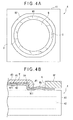
- the mounting sheet MS immediately before being heated by the slack removal unit 4 is bent so that the central portion of the mounting sheet MS comes closest to the wafer W before being attached on the wafer W. Accordingly, as shown in Fig. 4A , the mounting sheet MS has irregular waviness U (slack) in a form of ruffles between the wafer W and the ring frame RF. Further, as shown in Fig. 4B , a fifth space V5 (gap) may be present in addition to the fourth space V4.
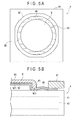
- the mounting sheet MS placed on the table 41 is heated by the slack removal unit 4, a stretch margin is generated on the mounting sheet MS. Then, as shown in Fig. 5B , the mounting sheet MS is closely attached on the wafer W due to pressure difference against the atmospheric pressure to eliminate the fourth and fifth spaces V4 and V5. Further, when the mounting sheet MS is heated, the mounting sheet MS is stretched in a direction in which tension is applied by the ring frame RF so that the waviness U is transformed into a plurality of lines SU extending in a predetermined direction, as shown in Fig. 5A .
- the multijoint robot 5 sucks and holds a part of the ring frame RF with the suction pads 59 and lifts up the mounting sheet MS from the table 41. Then, the mounting sheet MS is naturally cooled to an ambient temperature and the mounting sheet MS is drawn to be contracted by the tension of the ring frame RF to eliminate the lines SU and the slack emerged during the heating as shown in Figs. 6A and 6B . Thus, the displacement of the wafer W relative to the ring frame RF is no more allowed, thereby avoiding damages on the wafer W. It is speculated that the slack is eliminated due to a cause related to a residual stress remained in a base material of the mounting sheet MS that is generated when the base material is stretched for forming the mounting sheet MS.
- the wafer W and the ring frame RF are transferred by the multijoint robot 5 to a next step (e.g. step for peeling the protection sheet).
- the sheet adhering device 1 is adapted to heat the mounting sheet MS to transform the waviness U into the plurality of lines SU extending in a predetermined direction.
- the lines SU naturally cooled to be eliminated, thereby removing the slack.
- the slack removal unit 4 is provided outside the decompression unit 3, the slack-removal step of the mounting sheet MS attached on the wafer W and the attaching step of the next pair of the wafer W and the mounting sheet MS can be performed in an overlapped manner, so that the efficiency of the adhesion process per a unit time can be enhanced.
- the adherend is not restricted to the wafer W, and the ring frame RF may be omitted.
- the adherend may be a plate member such as a glass plate, steel plate and resin plate or a member that is not plate-shaped.
- the examples of the wafer W include silicon semiconductor wafer, a compound semiconductor wafer or the like.
- the adhesive sheet to be attached to the adherend may be, instead of the mounting sheet MS, an adhesive sheet for any application to be attached on a plate-shaped member and of any shape such as a sheet, film and tape.
- the wafer W attached with a protection sheet on a circuit face thereof is used in the above exemplary embodiment, the protection sheet may not be attached on the wafer W.
- the irregularities formed on the wafer W may be a bump (an electrode on a semiconductor chip) and the like instead of the convex portion W1.
- the sheet support is not limited to the cover member 6 and the lower chamber 7.
- the cover member 6 may be provided in a form of a box as in the lower chamber 7 and a table for supporting the ring frame RF and the mounting sheet MS may be provided on the lower face 61 of the cover member 6.
- an outer peripheral table may be provided on the bottom face 71 of the lower chamber 7 to surround the adherend support unit 2 and the mounting sheet MS attached with the ring frame RF may be supported on the table.
- the cover member 6, lower chamber 7 and multijoint robot 5 hold a part of the ring frame RF to hold the wafer W and the mounting sheet MS in the above exemplary embodiment, the mounting sheet MS may be held.
- the pressure in the first space V1 in which the wafer W is not present is set higher than the pressure in the second space V2 in which the wafer W is present by the pressure adjuster 8A to attach the mounting sheet MS on the wafer W.
- the mounting sheet MS may be pressed to be attached on the wafer W by a different pressing unit.
- the pressure in the second space V2 may be set lower than the pressure in the first space V1 by the pressure adjuster 8B.
- an attaching roller may be provided and the attaching roller may be rolled on the mounting sheet MS to attach the mounting sheet MS onto the wafer W.
- the pressing unit may be configured so that the mounting sheet MS is attached to the wafer W in an atmospheric pressure without keeping the first and second spaces V 1 and V2 in a decompressed atmosphere when the mounting sheet MS is attached to the wafer W.
- the wafer W integrated with the ring frame RF is placed on the table 41 so that the mounting sheet MS faces the mount face 41A of the table 41 and the slack removal unit 4 heats the mounting sheet MS
- the arrangement is not limited thereto.
- the wafer W and the ring frame RF may be placed on the table 41 to face the mount surface 41A, and the mounting sheet MS may be indirectly heated (directly or through air) by heating the wafer W and the ring frame RF with the slack removal unit 4.
- the gap removal unit 4 may be in any form as long as the mounting sheet MS can be directly or indirectly heated.
- infrared-ray irradiation equipment or microwave applicator may be used instead of the heater 42.
- a heating unit such as the heater 42 may be provided outside the table 41 and the mounting sheet MS may be heated by the heater 42 from above or from a lateral side.
- the slack removal unit 4 may be a component that is adapted to remove a slack of the mounting sheet MS in a process other than heating.
- the gap removal unit 4 may be provided by a cooler in a form of such a Peltier element and the like that is adapted to cool the mounting sheet MS.
- the table 21 of the adherend support unit 2 and the table 41 of the slack removal unit 4 are provided as independent components in the above exemplary embodiment, the table 21 of the adherend support unit 2 may have the heater or cooler therein to remove the slack.
- the mounting sheet MS attached to the wafer W is naturally cooled to remove the slack of the mounting sheet MS in the above exemplary embodiment
- the mounting sheet MS may alternatively be forcibly cooled with the use of a forcible cooler such as a fan and a cold-air blower.
- a forcible cooler such as a fan and a cold-air blower.
- the unit for transferring the wafer W is not limited to the multijoint robot 5.
- any transfer unit may be used as long as the wafer W attached with the mounting sheet MS is transferrable to the slack removal unit 4.
- the table 41 including the heater 42 may be provided to be slidably driven by a uniaxial robot and, when the cover member 6 is separated from the lower chamber 7, the table 41 may be moved between the cover member 6 and the lower chamber 7 to transfer the ring frame RF attached with the mounting sheet MS to the cover member 6 or the wafer W attached with the mounting sheet MS may be drawn out from the cover member 6.
- the drive unit mentioned in the above exemplary embodiment may be provided by: motorized equipment such as a rotary motor, linear movement motor, linear motor, uniaxial robot and multijoint robot; an actuator such as an air cylinder, hydraulic cylinder, rodless cylinder; or a direct or an indirect combination of the motorized equipment and/or actuator, which may be the same as those mentioned in the exemplary embodiment.
- motorized equipment such as a rotary motor, linear movement motor, linear motor, uniaxial robot and multijoint robot
- an actuator such as an air cylinder, hydraulic cylinder, rodless cylinder
- a direct or an indirect combination of the motorized equipment and/or actuator which may be the same as those mentioned in the exemplary embodiment.
Landscapes
- Container, Conveyance, Adherence, Positioning, Of Wafer (AREA)
Abstract
Description
- The present invention relates to a sheet adhering device and a sheet adhering method for attaching an adhesive sheet to an adherend.
- A sheet adhering device for integrating a semiconductor wafer (adherend: sometimes simply referred to as a "wafer" hereinafter) and a ring frame (frame) with the use of an adhesive sheet has conventionally been employed in a semiconductor manufacturing process (see, for instance, Patent Literature 1). Since the adhesive sheet has been attached to the ring frame in advance in the above sheet adhering device, the wafer and the ring frame can be easily integrated only by pressing to the wafer an adhesive layer of the adhesive sheet exposed at an opening of the ring frame.
-
- Patent Literature 1:
JP-A-2004-87660 - However, if the adhesive sheet attached to the ring frame is pulled toward the wafer when the adhesive sheet is pressed to the wafer, or if the wafer is pressed to the adhesive sheet at the opening of the ring frame, a tension is applied on the adhesive sheet, which causes a plastic deformation of the adhesive sheet between the adherend and the frame, thereby stretching (i.e. slacking) the adhesive sheet. Thus, since the adherend is integrated in a manner capable of displacement relative to the frame, the adherend cannot be reliably held and consequently may be damaged.
- An object of the invention is to provide a sheet adhering device and a sheet adhering method that is adapted to integrate an adhesive sheet with a frame without creating a slack between the adherend and the frame.
- In order to achieve an object of the invention, a sheet adhering device according to an aspect of the invention attaches an adhesive sheet to an adherend, the adhesive sheet being attached to an opening of a frame in advance and sized to protrude beyond an outer periphery of the adherend, the sheet adhering device including: a pressing unit that presses the adhesive sheet to the adherend to attach the adhesive sheet to the adherend; and a slack removal unit that removes a slack of a part of the adhesive sheet protruded beyond the outer periphery of the adherend after being attached by the pressing unit.
- In the sheet adhering device according to the above aspect of the invention, the slack removal unit is preferably adapted to heat or cool the adhesive sheet after the adhesive sheet is attached to the adherend.
- A sheet adhering method according to another aspect of the invention is for attaching an adhesive sheet to an adherend, the method including: attaching the adhesive sheet in advance to an opening of a frame, the adhesive sheet being sized to protrude beyond an outer periphery of the adherend; pressing the adhesive sheet attached to the opening of the frame to attach the adhesive sheet to the adherend; and removing a slack of the adherend after the adhesive sheet is attached to the adherend.
- According to the above aspect of the invention, since the slack removal unit is provided, the adhesive sheet can be integrated with the frame without creating a slack between the adherend and the frame. Thus, the adherend can be reliably held by the frame and a damage of the adherend can be prevented beforehand.
- In the above aspect of the invention, by heating or cooling the adhesive sheet after the adhesive sheet is attached to the adherend, the slack of the adhesive sheet between the adherend and the frame can be eliminated when the adhesive sheet is cooled/heated to an ambient temperature after being heated/cooled, so that the slack of the adhesive sheet between the adherend and the frame can be removed with a simple arrangement.
-
-
Fig. 1 is a partial sectional side elevation showing a sheet adhering device according to an exemplary embodiment of the invention. -
Fig. 2A is an illustration showing an operation of the sheet adhering device. -
Fig. 2B is another illustration showing the operation of the sheet adhering device. -
Fig. 2C is still another illustration showing the operation of the sheet adhering device. -
Fig. 3 is an illustration showing another operation of the sheet adhering device. -
Fig. 4A shows a condition of the adhesive sheet after being attached. -
Fig. 4B shows the condition of the adhesive sheet after being attached. -
Fig. 5A shows the condition of the adhesive sheet after being attached. -
Fig. 5B shows the condition of the adhesive sheet after being attached. -
Fig. 6A shows the condition of the adhesive sheet after being attached. -
Fig. 6B shows the condition of the adhesive sheet after being attached. - Exemplary embodiment(s) of the invention will be described below with reference to the attached drawings.
As shown inFig. 1 , asheet adhering device 1 according to this exemplary embodiment is for attaching a mounting sheet MS (adhesive sheet) that is attached in advance to close anopening RF 1 of a ring frame RF to a wafer W (adherend) to integrate the wafer W and the ring frame RF with the mounting sheet MS. The wafer W is a semiconductor wafer that is ground to provide an outer periphery thicker than the rest of the wafer, whereby an annular convex portion W1 protruded in the thickness direction (toward a back side) is defined on an outer periphery, a cavity W2 is defined at an inside surrounded by the convex portion W1 and a circuitry is formed on a circuit face W3 on a top side (i.e. a side opposite to the ground face and at a lower side inFig. 1 ) of the wafer W. A protection sheet (not shown) is attached on the circuit face W3. Further, the mounting sheet MS has a layered structure in which an adhesive layer is laminated on one side of a base material sheet (not shown). - As shown in
Fig. 1 , thesheet adhering device 1 includes: anadherend support unit 2 that supports the wafer W; adecompression unit 3 that holds the mounting sheet MS at a position opposing the wafer W and keeps the wafer W and the mounting sheet MS in a decompressed atmosphere; aslack removal unit 4 that is provided outside thedecompression unit 3 and heats the mounting sheet MS to remove a slack at a part of the mounting sheet MS protruding beyond an outer periphery of the wafer W; and a multijoint robot 5 (drive unit) that transfers the wafer W attached with the mounting sheet MS to theslack removal unit 4. - The
adherend support unit 2 includes a disc-shaped table 21 having a profile larger than an outer periphery of the wafer W, and a linear movement motor 22 (drive unit) having anoutput shaft 22A fixed on a lower face of the table 21. Anannular convex portion 23 of which an outer periphery protrudes in thickness direction (upward inFig. 1 ) is provided on anupper face 24 of the table 21. - The
decompression unit 3 includes acover member 6 and alower chamber 7 that support the mounting sheet MS attached on the ring frame RF in a manner opposed with the wafer W, apressure adjuster 8A (a pressing unit) that is adapted to decompress an inside of a first space V1 defined by thecover member 6 and the mounting sheet MS (seeFig. 2A ) and apressure adjuster 8B (a pressing unit) that is adapted to decompress an inside of a second space V2 (seeFig. 2A ) defined by the mounting sheet MS and thelower chamber 7. It should be noted that thecover member 6 and thelower chamber 7 provide a sheet support that supports the mounting sheet MS attached to the ring frame RF. - The
cover member 6 is capable of vertical movement by a drive unit (not shown). On alower face 61 of thecover member 6, aframe holder 63 having concave cross section with the same profile as an outer profile of the ring frame RF, and anelastic member 64 that is embedded in theframe holder 63 with a surface thereof being exposed on theframe holder 63 are provided. A part of theframe holder 63 under which the ring frame RF is located is provided with a plurality ofsuction holes 65 and is provided by an elastic member to keep the sealability of thefirst space V 1 by conforming with the height gap created by the mounting sheet MS. Apressure adjustment channel 66 connected to thepressure adjuster 8A is provided to theframe holder 63. Apressure detector 9A for detecting a pressure in the first space V1 is provided in thepressure adjustment channel 66. - The
lower chamber 7 is provided in a box shape having an opening at anupper face 74 thereof. Specifically, thelower chamber 7 includes abottom face 71 at which theadherend support unit 2 is provided and alateral face 72 extending upward from an outer periphery of thebottom face 71. Apressure adjustment channel 73 connected to thepressure adjuster 8B is provided to thebottom face 71. Apressure detector 9B for detecting a pressure in the second space V2 is provided in thepressure adjustment channel 73. A recessedannular support 75 is provided at an inner side of theupper face 74 of thelateral face 72. The ring frame RF attached with the mounting sheet MS is adapted to be supported by thesupport 75. - In the
decompression unit 3, the mounting sheet MS defines separate first space V1 and second space V2. Thepressure adjusters second spaces V 1 and V2 to press and attach the mounting sheet MS to the wafer W with the use of the differential pressure between the first space V1 and second space V2. - The
slack removal unit 4 includes a table 41 on which the wafer W integrated with the ring frame RF via the mounting sheet MS is placed and aheater 42 that is provided in the table 41 and is adapted to heat the mounting sheet MS. - The
multijoint robot 5 includes: a base 50; afirst arm 51 that is held on the base in a manner rotatable around a vertical axis PA (an axis in up-down direction) relative to thebase 50; asecond arm 52 that is pivotally supported on thefirst arm 51 in a manner rotatable around a horizontal axis orthogonal to the vertical axis PA (an axis orthogonal to a plane ofFig. 1 ); athird arm 53 pivotally supported on thesecond arm 52 in a manner rotatable around the horizontal axis; afourth arm 54 pivotally supported on thethird arm 53 in a manner rotatable around an extension axis EA of thethird arm 53; afifth arm 55 that is pivotally supported on thefourth arm 54 in a manner rotatable around an axis orthogonal to the extension axis EA (an axis orthogonal to the plane ofFig. 1 ); asixth arm 56 that is pivotally supported on thefifth arm 55 in a manner rotatable around an extension axis CA of thefifth arm 55; aframe 57 provided to thesixth arm 56; andsuction pads 59 provided via four holder arms 59 (partly not shown) vertically provided on theframe 57 and at an angular interval of 90 degrees. Themultijoint robot 5 is adapted to hold the wafer W and the ring frame RF integrated via the mounting sheet MS with thesuction pads 59. - A process for attaching the mounting sheet MS on the wafer W in the above-described
sheet adhering device 1 will be described below.
Initially, the ring frame RF in which the opening RF1 is closed by the mounting sheet MS is sucked and held on thecover member 6 and the wafer W is mounted on the table 21, with the use of a transfer unit (not shown) as shown inFig. 1 . Subsequently, thedecompression unit 3 lowers thecover member 6 by a drive unit (not shown) to bring thelower face 61 of thecover member 6 into contact with theupper face 74 of thelower chamber 7. After the first and second spaces V1 and V2 are defined by thecover member 6 and thelower chamber 7, thepressure adjusters second spaces V 1 and V2 so that the pressures in the first andsecond spaces V 1 and V2 are equalized while decompressing the first andsecond spaces V 1 and V2 at an equal decompression rate. - Next, the
decompression unit 3 sets the pressure in the first space V1 to be higher than the pressure in the second space V2 by thepressure adjusters Fig. 2A , the mounting sheet MS is urged toward the second space V2 due to the differential pressure between the first and thesecond spaces V 1 and V2 and is bent so that a central part thereof comes closest to the wafer W. In this condition, when thelinear movement motor 22 is driven to elevate the table 21, the mounting sheet MS is gradually attached on the wafer W from a central portion to an outer periphery of the wafer W as shown inFig. 2B . Then, as shown inFig. 2C , when the mounting sheet MS is pressed and is kept being pressed onto theelastic member 64 of thecover member 6 by the top face W11 of the convex portion W1, a new third space V3 is created in the first space V1 and between an inside of theelastic member 64 and the mounting sheet MS and a new fourth space V4 (gap) is created in the second space V2 and between the mounting sheet MS and the wafer W. - Subsequently, the pressure in the second space V2 is set to be equal to the pressure in the first space V1 by the
pressure adjuster 8B. Then, thedecompression unit 3 increases the pressures in the third and second spaces V3 and V2 with thepressure adjusters Fig. 3 ). Then, while the ring frame RF is sucked and held via the suction holes 65, thedecompression unit 3 lifts thecover member 6 to a predetermined level with the use of a drive unit (not shown). As shown inFig. 3 , themultijoint robot 5 sucks and holds a part of the ring frame RF with thesuction pads 59 and places the wafer W on the table 41 with the mounting sheet MS facing amount face 41 A of the table 41. - The mounting sheet MS immediately before being heated by the
slack removal unit 4 is bent so that the central portion of the mounting sheet MS comes closest to the wafer W before being attached on the wafer W. Accordingly, as shown inFig. 4A , the mounting sheet MS has irregular waviness U (slack) in a form of ruffles between the wafer W and the ring frame RF. Further, as shown inFig. 4B , a fifth space V5 (gap) may be present in addition to the fourth space V4. - When the mounting sheet MS placed on the table 41 is heated by the
slack removal unit 4, a stretch margin is generated on the mounting sheet MS. Then, as shown inFig. 5B , the mounting sheet MS is closely attached on the wafer W due to pressure difference against the atmospheric pressure to eliminate the fourth and fifth spaces V4 and V5.
Further, when the mounting sheet MS is heated, the mounting sheet MS is stretched in a direction in which tension is applied by the ring frame RF so that the waviness U is transformed into a plurality of lines SU extending in a predetermined direction, as shown inFig. 5A . - After a predetermined time elapsed, the
multijoint robot 5 sucks and holds a part of the ring frame RF with thesuction pads 59 and lifts up the mounting sheet MS from the table 41. Then, the mounting sheet MS is naturally cooled to an ambient temperature and the mounting sheet MS is drawn to be contracted by the tension of the ring frame RF to eliminate the lines SU and the slack emerged during the heating as shown inFigs. 6A and 6B . Thus, the displacement of the wafer W relative to the ring frame RF is no more allowed, thereby avoiding damages on the wafer W. It is speculated that the slack is eliminated due to a cause related to a residual stress remained in a base material of the mounting sheet MS that is generated when the base material is stretched for forming the mounting sheet MS. - When the mounting sheet MS is completely attached as discussed above and the wafer W and the ring frame RF are integrated via the mounting sheet MS, the wafer W and the ring frame RF are transferred by the
multijoint robot 5 to a next step (e.g. step for peeling the protection sheet). - According to the above-described exemplary embodiment, the following advantages can be obtained.
Even if the waviness U is generated between the wafer W and the ring frame RF when the mounting sheet MS is attached to the wafer W, thesheet adhering device 1 is adapted to heat the mounting sheet MS to transform the waviness U into the plurality of lines SU extending in a predetermined direction. The lines SU naturally cooled to be eliminated, thereby removing the slack.
Further, since theslack removal unit 4 is provided outside thedecompression unit 3, the slack-removal step of the mounting sheet MS attached on the wafer W and the attaching step of the next pair of the wafer W and the mounting sheet MS can be performed in an overlapped manner, so that the efficiency of the adhesion process per a unit time can be enhanced. - The best arrangement and process for implementing the invention has been described above. However, it should be understood that the scope of the invention is not limited to the above exemplary embodiment. In other words, while the invention has been particularly explained and illustrated mainly in relation to a specific embodiment, a person skilled in the art could make various modifications in terms of shape, material, quantity or other particulars to the above described embodiment without deviating from the technical idea or any object of the present invention. Further, any descriptions of shape, material or quantity or the like disclosed above are given as examples to enable easy understanding of the invention, and do not limit the present invention, so that descriptions using names of components, with any such limitations of shape, material or quantity or the like removed in part or whole, are included in the present invention.
- For instance, though an example in which the adherend is the wafer W is discussed in the above exemplary embodiment, the adherend is not restricted to the wafer W, and the ring frame RF may be omitted. Alternatively, the adherend may be a plate member such as a glass plate, steel plate and resin plate or a member that is not plate-shaped. The examples of the wafer W include silicon semiconductor wafer, a compound semiconductor wafer or the like. The adhesive sheet to be attached to the adherend may be, instead of the mounting sheet MS, an adhesive sheet for any application to be attached on a plate-shaped member and of any shape such as a sheet, film and tape. Further, though the wafer W attached with a protection sheet on a circuit face thereof is used in the above exemplary embodiment, the protection sheet may not be attached on the wafer W. Further, the irregularities formed on the wafer W may be a bump (an electrode on a semiconductor chip) and the like instead of the convex portion W1.
- Though the mounting sheet MS attached with the ring frame RF is supported by the
cover member 6 and thelower chamber 7 of thedecompression unit 3 in the above exemplary embodiment, the sheet support is not limited to thecover member 6 and thelower chamber 7. For instance, thecover member 6 may be provided in a form of a box as in thelower chamber 7 and a table for supporting the ring frame RF and the mounting sheet MS may be provided on thelower face 61 of thecover member 6. Alternatively, an outer peripheral table may be provided on thebottom face 71 of thelower chamber 7 to surround theadherend support unit 2 and the mounting sheet MS attached with the ring frame RF may be supported on the table.
Further, though thecover member 6,lower chamber 7 andmultijoint robot 5 hold a part of the ring frame RF to hold the wafer W and the mounting sheet MS in the above exemplary embodiment, the mounting sheet MS may be held. - In the above exemplary embodiment, the pressure in the first space V1 in which the wafer W is not present is set higher than the pressure in the second space V2 in which the wafer W is present by the
pressure adjuster 8A to attach the mounting sheet MS on the wafer W. However, the mounting sheet MS may be pressed to be attached on the wafer W by a different pressing unit. For instance, the pressure in the second space V2 may be set lower than the pressure in the first space V1 by thepressure adjuster 8B. Alternatively, an attaching roller may be provided and the attaching roller may be rolled on the mounting sheet MS to attach the mounting sheet MS onto the wafer W. Alternatively, the pressing unit may be configured so that the mounting sheet MS is attached to the wafer W in an atmospheric pressure without keeping the first andsecond spaces V 1 and V2 in a decompressed atmosphere when the mounting sheet MS is attached to the wafer W. - Though the wafer W integrated with the ring frame RF is placed on the table 41 so that the mounting sheet MS faces the
mount face 41A of the table 41 and theslack removal unit 4 heats the mounting sheet MS, the arrangement is not limited thereto. For instance, in a manner opposite to the exemplary embodiment, the wafer W and the ring frame RF may be placed on the table 41 to face themount surface 41A, and the mounting sheet MS may be indirectly heated (directly or through air) by heating the wafer W and the ring frame RF with theslack removal unit 4. - Further, though the
heater 42 is used as theslack removal unit 4 in the above exemplary embodiment, the arrangement is not limited thereto. In other words, thegap removal unit 4 may be in any form as long as the mounting sheet MS can be directly or indirectly heated. For instance, infrared-ray irradiation equipment or microwave applicator may be used instead of theheater 42. Further, a heating unit such as theheater 42 may be provided outside the table 41 and the mounting sheet MS may be heated by theheater 42 from above or from a lateral side.
Theslack removal unit 4 may be a component that is adapted to remove a slack of the mounting sheet MS in a process other than heating. For instance, when the base material of the mounting sheet MS is provided by a rubber that is more stretchable when being cooled, thegap removal unit 4 may be provided by a cooler in a form of such a Peltier element and the like that is adapted to cool the mounting sheet MS.
Further, though the table 21 of theadherend support unit 2 and the table 41 of theslack removal unit 4 are provided as independent components in the above exemplary embodiment, the table 21 of theadherend support unit 2 may have the heater or cooler therein to remove the slack.
Further, though the mounting sheet MS attached to the wafer W is naturally cooled to remove the slack of the mounting sheet MS in the above exemplary embodiment, the mounting sheet MS may alternatively be forcibly cooled with the use of a forcible cooler such as a fan and a cold-air blower. Incidentally, when the mounting sheet MS is of characteristics that the waviness U is transformed into a plurality of lines SU as shown inFig. 5A when the mounting sheet MS is cooled and the lines SU are subsequently eliminated to remove the slack when the mounting sheet MS is naturally heated (i.e. temperature-raised), a heater, an infrared ray irradiator, a microwave applicator and the like may be used as a forcible heater. - Though the
multijoint robot 5 is used in the above exemplary embodiment, the unit for transferring the wafer W is not limited to themultijoint robot 5. In other words, any transfer unit may be used as long as the wafer W attached with the mounting sheet MS is transferrable to theslack removal unit 4. For instance, the table 41 including theheater 42 may be provided to be slidably driven by a uniaxial robot and, when thecover member 6 is separated from thelower chamber 7, the table 41 may be moved between thecover member 6 and thelower chamber 7 to transfer the ring frame RF attached with the mounting sheet MS to thecover member 6 or the wafer W attached with the mounting sheet MS may be drawn out from thecover member 6. - Further, the drive unit mentioned in the above exemplary embodiment may be provided by: motorized equipment such as a rotary motor, linear movement motor, linear motor, uniaxial robot and multijoint robot; an actuator such as an air cylinder, hydraulic cylinder, rodless cylinder; or a direct or an indirect combination of the motorized equipment and/or actuator, which may be the same as those mentioned in the exemplary embodiment.
-
EXPLANATION OF CODES 1 sheet adhering device 4 slack removal unit 8A,8B pressure adjuster (pressing unit) MS mounting sheet (adhesive sheet) RF ring frame (frame) W wafer (adherend)
Claims (3)
- A sheet adhering device that attaches an adhesive sheet to an adherend, the adhesive sheet being attached to an opening of a frame in advance and sized to protrude beyond an outer periphery of the adherend, the sheet adhering device comprising:a pressing unit that presses the adhesive sheet to the adherend to attach the adhesive sheet to the adherend; anda slack removal unit that removes a slack of a part of the adhesive sheet protruded beyond the outer periphery of the adherend after being attached by the pressing unit.
- The sheet adhering device according to claim 1, wherein the slack removal unit is adapted to heat or cool the adhesive sheet after the adhesive sheet is attached to the adherend.
- A sheet adhering method for attaching an adhesive sheet to an adherend, the method comprising:attaching the adhesive sheet in advance to an opening of a frame, the adhesive sheet being sized to protrude beyond an outer periphery of the adherend;pressing the adhesive sheet attached to the opening of the frame to attach the adhesive sheet to the adherend; andremoving a slack of the adherend after the adhesive sheet is attached to the adherend.
Applications Claiming Priority (2)
| Application Number | Priority Date | Filing Date | Title |
|---|---|---|---|
| JP2010189689A JP5542583B2 (en) | 2010-08-26 | 2010-08-26 | Sheet sticking device and sticking method |
| PCT/JP2011/067212 WO2012026275A1 (en) | 2010-08-26 | 2011-07-28 | Sheet adhering device and adhering method |
Publications (3)
| Publication Number | Publication Date |
|---|---|
| EP2610902A1 true EP2610902A1 (en) | 2013-07-03 |
| EP2610902A4 EP2610902A4 (en) | 2014-01-01 |
| EP2610902B1 EP2610902B1 (en) | 2020-01-01 |
Family
ID=45723283
Family Applications (1)
| Application Number | Title | Priority Date | Filing Date |
|---|---|---|---|
| EP11819740.9A Active EP2610902B1 (en) | 2010-08-26 | 2011-07-28 | Sheet adhering device and adhering method |
Country Status (6)
| Country | Link |
|---|---|
| EP (1) | EP2610902B1 (en) |
| JP (1) | JP5542583B2 (en) |
| KR (1) | KR101744371B1 (en) |
| CN (1) | CN103069562B (en) |
| TW (1) | TWI537138B (en) |
| WO (1) | WO2012026275A1 (en) |
Cited By (1)
| Publication number | Priority date | Publication date | Assignee | Title |
|---|---|---|---|---|
| US9324581B2 (en) | 2012-04-09 | 2016-04-26 | Mitsubishi Electric Corporation | Method for manufacturing semiconductor device |
Families Citing this family (10)
| Publication number | Priority date | Publication date | Assignee | Title |
|---|---|---|---|---|
| JP6543152B2 (en) * | 2015-09-30 | 2019-07-10 | リンテック株式会社 | Sheet sticking apparatus, sticking method, and adhesive sheet material |
| JP2017092313A (en) * | 2015-11-12 | 2017-05-25 | 株式会社東芝 | Semiconductor manufacturing equipment. |
| JP7108516B2 (en) * | 2018-10-25 | 2022-07-28 | リンテック株式会社 | Sheet pasting method |
| JP7684809B2 (en) * | 2020-06-09 | 2025-05-28 | 日東電工株式会社 | Adhesive sheet application method, adhesive sheet application device, and semiconductor product manufacturing method |
| TWI888536B (en) * | 2020-06-09 | 2025-07-01 | 日商日東電工股份有限公司 | Method for joining adhesive sheet, apparatus for joining adhesive sheet, and manufacturing method of semiconductor products |
| KR102194993B1 (en) | 2020-09-07 | 2020-12-28 | (주)엠엑스앤 | Vacuum chamber for attaching cooling sheet to focusing ring for manufacturing semiconductor device |
| KR102194996B1 (en) | 2020-09-07 | 2020-12-28 | (주)엠엑스앤 | Cooling sheet attachment apparatus of focusing ring for semiconductor device manufacturing |
| KR102214048B1 (en) | 2020-12-04 | 2021-02-10 | (주)엠엑스앤 | Cooling sheet attachment apparatus to focusing ring for semiconductor manufacturing apparatus |
| JP7653844B2 (en) * | 2021-06-11 | 2025-03-31 | 株式会社ディスコ | Annular protrusion removal device |
| JP2024032125A (en) * | 2022-08-29 | 2024-03-12 | 株式会社ディスコ | Pasting method |
Family Cites Families (11)
| Publication number | Priority date | Publication date | Assignee | Title |
|---|---|---|---|---|
| JP4744742B2 (en) * | 2001-08-06 | 2011-08-10 | 株式会社ディスコ | Workpiece division processing method and chip interval expansion apparatus used in the division processing method |
| JP4037218B2 (en) * | 2002-08-26 | 2008-01-23 | 株式会社タカトリ | Method and apparatus for transferring wafer to dicing tape |
| US7552528B2 (en) * | 2004-05-24 | 2009-06-30 | Panasonic Corporation | Wafer expanding device, component feeder, and expanding method for wafer sheet |
| JP2007027562A (en) * | 2005-07-20 | 2007-02-01 | Disco Abrasive Syst Ltd | Breaking method of adhesive film attached to wafer |
| JP2007134527A (en) * | 2005-11-11 | 2007-05-31 | Matsushita Electric Ind Co Ltd | Expanding device and semiconductor device manufacturing method |
| JP4632313B2 (en) * | 2006-05-18 | 2011-02-16 | リンテック株式会社 | Pasting device and pasting method |
| JP4841355B2 (en) * | 2006-08-08 | 2011-12-21 | 日東電工株式会社 | Method for holding semiconductor wafer |
| JP4733069B2 (en) * | 2007-05-22 | 2011-07-27 | リンテック株式会社 | Sheet sticking device and sticking method |
| JP5117934B2 (en) * | 2008-06-06 | 2013-01-16 | リンテック株式会社 | MOUNTING DEVICE AND MOUNTING METHOD |
| JP5006300B2 (en) * | 2008-10-23 | 2012-08-22 | リンテック株式会社 | MOUNTING DEVICE AND MOUNTING METHOD |
| JP5317267B2 (en) * | 2008-11-14 | 2013-10-16 | 株式会社タカトリ | Wafer mounting device |
-
2010
- 2010-08-26 JP JP2010189689A patent/JP5542583B2/en active Active
-
2011
- 2011-07-28 CN CN201180041312.1A patent/CN103069562B/en active Active
- 2011-07-28 EP EP11819740.9A patent/EP2610902B1/en active Active
- 2011-07-28 KR KR1020137007095A patent/KR101744371B1/en active Active
- 2011-07-28 WO PCT/JP2011/067212 patent/WO2012026275A1/en not_active Ceased
- 2011-08-02 TW TW100127305A patent/TWI537138B/en active
Non-Patent Citations (2)
| Title |
|---|
| No further relevant documents disclosed * |
| See also references of WO2012026275A1 * |
Cited By (1)
| Publication number | Priority date | Publication date | Assignee | Title |
|---|---|---|---|---|
| US9324581B2 (en) | 2012-04-09 | 2016-04-26 | Mitsubishi Electric Corporation | Method for manufacturing semiconductor device |
Also Published As
| Publication number | Publication date |
|---|---|
| TWI537138B (en) | 2016-06-11 |
| JP5542583B2 (en) | 2014-07-09 |
| JP2012049319A (en) | 2012-03-08 |
| EP2610902A4 (en) | 2014-01-01 |
| EP2610902B1 (en) | 2020-01-01 |
| TW201208881A (en) | 2012-03-01 |
| KR20130100137A (en) | 2013-09-09 |
| CN103069562B (en) | 2016-05-04 |
| KR101744371B1 (en) | 2017-06-07 |
| WO2012026275A1 (en) | 2012-03-01 |
| CN103069562A (en) | 2013-04-24 |
Similar Documents
| Publication | Publication Date | Title |
|---|---|---|
| EP2610902B1 (en) | Sheet adhering device and adhering method | |
| EP2610901B1 (en) | Sheet attaching device and attaching method | |
| EP2631938A1 (en) | Sheet adhesion device and adhesion method | |
| JP4781802B2 (en) | Support plate laminating means and laminating apparatus, and support plate laminating method | |
| KR102759515B1 (en) | Method for processing wafer | |
| JP4740297B2 (en) | MOUNTING DEVICE AND MOUNTING METHOD | |
| JP6636696B2 (en) | Semiconductor wafer mounting method and semiconductor wafer mounting apparatus | |
| JP2004153159A (en) | Protection member adhering method for semiconductor wafer and its device | |
| TWI639671B (en) | Adhesive tape sticking method and adhesive tape sticking device | |
| TW200816363A (en) | Semiconductor wafer holding method, semiconductor wafer holding apparatus and semiconductor wafer holding structure | |
| TW201946208A (en) | Application apparatus and application method for applying protective tape to a semiconductor wafer | |
| CN103681228A (en) | Adhesive tape joining method and adhesive tape joining apparatus | |
| JP7640158B2 (en) | Substrate bonding apparatus and substrate bonding method | |
| JP2004186482A (en) | Method and apparatus for attaching thermal adhesive film | |
| TW201501215A (en) | Sealing sheet attaching method and sealing sheet attaching device | |
| JP4839284B2 (en) | Method of attaching protective tape for peeling off protective sheet of plate-like member such as semiconductor wafer and method of peeling off protective sheet | |
| JP2022122403A (en) | Substrate bonding device and substrate bonding method | |
| KR101678352B1 (en) | Attaching apparatus | |
| JP5973203B2 (en) | Sheet sticking device and sticking method | |
| WO2015087763A1 (en) | Sealing sheet adhesion method | |
| KR20210122132A (en) | Device sealing method, device sealing apparatus, and manufacturing method of semiconductor products |
Legal Events
| Date | Code | Title | Description |
|---|---|---|---|
| PUAI | Public reference made under article 153(3) epc to a published international application that has entered the european phase |
Free format text: ORIGINAL CODE: 0009012 |
|
| 17P | Request for examination filed |
Effective date: 20130221 |
|
| AK | Designated contracting states |
Kind code of ref document: A1 Designated state(s): AL AT BE BG CH CY CZ DE DK EE ES FI FR GB GR HR HU IE IS IT LI LT LU LV MC MK MT NL NO PL PT RO RS SE SI SK SM TR |
|
| DAX | Request for extension of the european patent (deleted) | ||
| A4 | Supplementary search report drawn up and despatched |
Effective date: 20131128 |
|
| RIC1 | Information provided on ipc code assigned before grant |
Ipc: H01L 21/683 20060101AFI20131122BHEP |
|
| REG | Reference to a national code |
Ref country code: DE Ref legal event code: R079 Ref document number: 602011064390 Country of ref document: DE Free format text: PREVIOUS MAIN CLASS: H01L0021683000 Ipc: H01L0021670000 |
|
| STAA | Information on the status of an ep patent application or granted ep patent |
Free format text: STATUS: EXAMINATION IS IN PROGRESS |
|
| 17Q | First examination report despatched |
Effective date: 20190318 |
|
| RIC1 | Information provided on ipc code assigned before grant |
Ipc: H01L 21/67 20060101AFI20190312BHEP |
|
| GRAP | Despatch of communication of intention to grant a patent |
Free format text: ORIGINAL CODE: EPIDOSNIGR1 |
|
| STAA | Information on the status of an ep patent application or granted ep patent |
Free format text: STATUS: GRANT OF PATENT IS INTENDED |
|
| INTG | Intention to grant announced |
Effective date: 20190926 |
|
| GRAS | Grant fee paid |
Free format text: ORIGINAL CODE: EPIDOSNIGR3 |
|
| GRAA | (expected) grant |
Free format text: ORIGINAL CODE: 0009210 |
|
| STAA | Information on the status of an ep patent application or granted ep patent |
Free format text: STATUS: THE PATENT HAS BEEN GRANTED |
|
| AK | Designated contracting states |
Kind code of ref document: B1 Designated state(s): AL AT BE BG CH CY CZ DE DK EE ES FI FR GB GR HR HU IE IS IT LI LT LU LV MC MK MT NL NO PL PT RO RS SE SI SK SM TR |
|
| REG | Reference to a national code |
Ref country code: GB Ref legal event code: FG4D |
|
| REG | Reference to a national code |
Ref country code: CH Ref legal event code: EP Ref country code: AT Ref legal event code: REF Ref document number: 1220856 Country of ref document: AT Kind code of ref document: T Effective date: 20200115 |
|
| REG | Reference to a national code |
Ref country code: IE Ref legal event code: FG4D |
|
| REG | Reference to a national code |
Ref country code: DE Ref legal event code: R096 Ref document number: 602011064390 Country of ref document: DE |
|
| REG | Reference to a national code |
Ref country code: NL Ref legal event code: MP Effective date: 20200101 |
|
| REG | Reference to a national code |
Ref country code: LT Ref legal event code: MG4D |
|
| PG25 | Lapsed in a contracting state [announced via postgrant information from national office to epo] |
Ref country code: FI Free format text: LAPSE BECAUSE OF FAILURE TO SUBMIT A TRANSLATION OF THE DESCRIPTION OR TO PAY THE FEE WITHIN THE PRESCRIBED TIME-LIMIT Effective date: 20200101 Ref country code: NO Free format text: LAPSE BECAUSE OF FAILURE TO SUBMIT A TRANSLATION OF THE DESCRIPTION OR TO PAY THE FEE WITHIN THE PRESCRIBED TIME-LIMIT Effective date: 20200401 Ref country code: LT Free format text: LAPSE BECAUSE OF FAILURE TO SUBMIT A TRANSLATION OF THE DESCRIPTION OR TO PAY THE FEE WITHIN THE PRESCRIBED TIME-LIMIT Effective date: 20200101 Ref country code: RS Free format text: LAPSE BECAUSE OF FAILURE TO SUBMIT A TRANSLATION OF THE DESCRIPTION OR TO PAY THE FEE WITHIN THE PRESCRIBED TIME-LIMIT Effective date: 20200101 Ref country code: PT Free format text: LAPSE BECAUSE OF FAILURE TO SUBMIT A TRANSLATION OF THE DESCRIPTION OR TO PAY THE FEE WITHIN THE PRESCRIBED TIME-LIMIT Effective date: 20200527 Ref country code: NL Free format text: LAPSE BECAUSE OF FAILURE TO SUBMIT A TRANSLATION OF THE DESCRIPTION OR TO PAY THE FEE WITHIN THE PRESCRIBED TIME-LIMIT Effective date: 20200101 Ref country code: CZ Free format text: LAPSE BECAUSE OF FAILURE TO SUBMIT A TRANSLATION OF THE DESCRIPTION OR TO PAY THE FEE WITHIN THE PRESCRIBED TIME-LIMIT Effective date: 20200101 |
|
| PG25 | Lapsed in a contracting state [announced via postgrant information from national office to epo] |
Ref country code: BG Free format text: LAPSE BECAUSE OF FAILURE TO SUBMIT A TRANSLATION OF THE DESCRIPTION OR TO PAY THE FEE WITHIN THE PRESCRIBED TIME-LIMIT Effective date: 20200401 Ref country code: GR Free format text: LAPSE BECAUSE OF FAILURE TO SUBMIT A TRANSLATION OF THE DESCRIPTION OR TO PAY THE FEE WITHIN THE PRESCRIBED TIME-LIMIT Effective date: 20200402 Ref country code: SE Free format text: LAPSE BECAUSE OF FAILURE TO SUBMIT A TRANSLATION OF THE DESCRIPTION OR TO PAY THE FEE WITHIN THE PRESCRIBED TIME-LIMIT Effective date: 20200101 Ref country code: LV Free format text: LAPSE BECAUSE OF FAILURE TO SUBMIT A TRANSLATION OF THE DESCRIPTION OR TO PAY THE FEE WITHIN THE PRESCRIBED TIME-LIMIT Effective date: 20200101 Ref country code: IS Free format text: LAPSE BECAUSE OF FAILURE TO SUBMIT A TRANSLATION OF THE DESCRIPTION OR TO PAY THE FEE WITHIN THE PRESCRIBED TIME-LIMIT Effective date: 20200501 Ref country code: HR Free format text: LAPSE BECAUSE OF FAILURE TO SUBMIT A TRANSLATION OF THE DESCRIPTION OR TO PAY THE FEE WITHIN THE PRESCRIBED TIME-LIMIT Effective date: 20200101 |
|
| REG | Reference to a national code |
Ref country code: DE Ref legal event code: R097 Ref document number: 602011064390 Country of ref document: DE |
|
| PG25 | Lapsed in a contracting state [announced via postgrant information from national office to epo] |
Ref country code: DK Free format text: LAPSE BECAUSE OF FAILURE TO SUBMIT A TRANSLATION OF THE DESCRIPTION OR TO PAY THE FEE WITHIN THE PRESCRIBED TIME-LIMIT Effective date: 20200101 Ref country code: ES Free format text: LAPSE BECAUSE OF FAILURE TO SUBMIT A TRANSLATION OF THE DESCRIPTION OR TO PAY THE FEE WITHIN THE PRESCRIBED TIME-LIMIT Effective date: 20200101 Ref country code: SK Free format text: LAPSE BECAUSE OF FAILURE TO SUBMIT A TRANSLATION OF THE DESCRIPTION OR TO PAY THE FEE WITHIN THE PRESCRIBED TIME-LIMIT Effective date: 20200101 Ref country code: RO Free format text: LAPSE BECAUSE OF FAILURE TO SUBMIT A TRANSLATION OF THE DESCRIPTION OR TO PAY THE FEE WITHIN THE PRESCRIBED TIME-LIMIT Effective date: 20200101 Ref country code: EE Free format text: LAPSE BECAUSE OF FAILURE TO SUBMIT A TRANSLATION OF THE DESCRIPTION OR TO PAY THE FEE WITHIN THE PRESCRIBED TIME-LIMIT Effective date: 20200101 Ref country code: SM Free format text: LAPSE BECAUSE OF FAILURE TO SUBMIT A TRANSLATION OF THE DESCRIPTION OR TO PAY THE FEE WITHIN THE PRESCRIBED TIME-LIMIT Effective date: 20200101 |
|
| PLBE | No opposition filed within time limit |
Free format text: ORIGINAL CODE: 0009261 |
|
| STAA | Information on the status of an ep patent application or granted ep patent |
Free format text: STATUS: NO OPPOSITION FILED WITHIN TIME LIMIT |
|
| 26N | No opposition filed |
Effective date: 20201002 |
|
| PG25 | Lapsed in a contracting state [announced via postgrant information from national office to epo] |
Ref country code: IT Free format text: LAPSE BECAUSE OF FAILURE TO SUBMIT A TRANSLATION OF THE DESCRIPTION OR TO PAY THE FEE WITHIN THE PRESCRIBED TIME-LIMIT Effective date: 20200101 |
|
| PG25 | Lapsed in a contracting state [announced via postgrant information from national office to epo] |
Ref country code: SI Free format text: LAPSE BECAUSE OF FAILURE TO SUBMIT A TRANSLATION OF THE DESCRIPTION OR TO PAY THE FEE WITHIN THE PRESCRIBED TIME-LIMIT Effective date: 20200101 Ref country code: PL Free format text: LAPSE BECAUSE OF FAILURE TO SUBMIT A TRANSLATION OF THE DESCRIPTION OR TO PAY THE FEE WITHIN THE PRESCRIBED TIME-LIMIT Effective date: 20200101 Ref country code: MC Free format text: LAPSE BECAUSE OF FAILURE TO SUBMIT A TRANSLATION OF THE DESCRIPTION OR TO PAY THE FEE WITHIN THE PRESCRIBED TIME-LIMIT Effective date: 20200101 |
|
| REG | Reference to a national code |
Ref country code: CH Ref legal event code: PL |
|
| REG | Reference to a national code |
Ref country code: AT Ref legal event code: UEP Ref document number: 1220856 Country of ref document: AT Kind code of ref document: T Effective date: 20200101 |
|
| REG | Reference to a national code |
Ref country code: BE Ref legal event code: MM Effective date: 20200731 |
|
| PG25 | Lapsed in a contracting state [announced via postgrant information from national office to epo] |
Ref country code: LU Free format text: LAPSE BECAUSE OF NON-PAYMENT OF DUE FEES Effective date: 20200728 Ref country code: FR Free format text: LAPSE BECAUSE OF NON-PAYMENT OF DUE FEES Effective date: 20200731 Ref country code: CH Free format text: LAPSE BECAUSE OF NON-PAYMENT OF DUE FEES Effective date: 20200731 Ref country code: LI Free format text: LAPSE BECAUSE OF NON-PAYMENT OF DUE FEES Effective date: 20200731 |
|
| PG25 | Lapsed in a contracting state [announced via postgrant information from national office to epo] |
Ref country code: BE Free format text: LAPSE BECAUSE OF NON-PAYMENT OF DUE FEES Effective date: 20200731 |
|
| PG25 | Lapsed in a contracting state [announced via postgrant information from national office to epo] |
Ref country code: IE Free format text: LAPSE BECAUSE OF NON-PAYMENT OF DUE FEES Effective date: 20200728 |
|
| PG25 | Lapsed in a contracting state [announced via postgrant information from national office to epo] |
Ref country code: TR Free format text: LAPSE BECAUSE OF FAILURE TO SUBMIT A TRANSLATION OF THE DESCRIPTION OR TO PAY THE FEE WITHIN THE PRESCRIBED TIME-LIMIT Effective date: 20200101 Ref country code: MT Free format text: LAPSE BECAUSE OF FAILURE TO SUBMIT A TRANSLATION OF THE DESCRIPTION OR TO PAY THE FEE WITHIN THE PRESCRIBED TIME-LIMIT Effective date: 20200101 Ref country code: CY Free format text: LAPSE BECAUSE OF FAILURE TO SUBMIT A TRANSLATION OF THE DESCRIPTION OR TO PAY THE FEE WITHIN THE PRESCRIBED TIME-LIMIT Effective date: 20200101 |
|
| PG25 | Lapsed in a contracting state [announced via postgrant information from national office to epo] |
Ref country code: MK Free format text: LAPSE BECAUSE OF FAILURE TO SUBMIT A TRANSLATION OF THE DESCRIPTION OR TO PAY THE FEE WITHIN THE PRESCRIBED TIME-LIMIT Effective date: 20200101 Ref country code: AL Free format text: LAPSE BECAUSE OF FAILURE TO SUBMIT A TRANSLATION OF THE DESCRIPTION OR TO PAY THE FEE WITHIN THE PRESCRIBED TIME-LIMIT Effective date: 20200101 |
|
| P01 | Opt-out of the competence of the unified patent court (upc) registered |
Effective date: 20231218 |
|
| PGFP | Annual fee paid to national office [announced via postgrant information from national office to epo] |
Ref country code: DE Payment date: 20250722 Year of fee payment: 15 |
|
| PGFP | Annual fee paid to national office [announced via postgrant information from national office to epo] |
Ref country code: GB Payment date: 20250722 Year of fee payment: 15 |
|
| PGFP | Annual fee paid to national office [announced via postgrant information from national office to epo] |
Ref country code: AT Payment date: 20250722 Year of fee payment: 15 |
|
| REG | Reference to a national code |
Ref country code: DE Ref legal event code: R079 Ref document number: 602011064390 Country of ref document: DE Free format text: PREVIOUS MAIN CLASS: H01L0021670000 Ipc: H10P0072000000 |