EP2610643B1 - Détecteur de rayonnement - Google Patents
Détecteur de rayonnement Download PDFInfo
- Publication number
- EP2610643B1 EP2610643B1 EP11819660.9A EP11819660A EP2610643B1 EP 2610643 B1 EP2610643 B1 EP 2610643B1 EP 11819660 A EP11819660 A EP 11819660A EP 2610643 B1 EP2610643 B1 EP 2610643B1
- Authority
- EP
- European Patent Office
- Prior art keywords
- scintillator layer
- substrate
- supporting substrate
- light detection
- layer
- Prior art date
- Legal status (The legal status is an assumption and is not a legal conclusion. Google has not performed a legal analysis and makes no representation as to the accuracy of the status listed.)
- Active
Links
Images



Classifications
-
- G—PHYSICS
- G01—MEASURING; TESTING
- G01T—MEASUREMENT OF NUCLEAR OR X-RADIATION
- G01T1/00—Measuring X-radiation, gamma radiation, corpuscular radiation, or cosmic radiation
- G01T1/16—Measuring radiation intensity
- G01T1/20—Measuring radiation intensity with scintillation detectors
-
- G—PHYSICS
- G01—MEASURING; TESTING
- G01T—MEASUREMENT OF NUCLEAR OR X-RADIATION
- G01T1/00—Measuring X-radiation, gamma radiation, corpuscular radiation, or cosmic radiation
- G01T1/16—Measuring radiation intensity
- G01T1/20—Measuring radiation intensity with scintillation detectors
- G01T1/2006—Measuring radiation intensity with scintillation detectors using a combination of a scintillator and photodetector which measures the means radiation intensity
-
- G—PHYSICS
- G01—MEASURING; TESTING
- G01T—MEASUREMENT OF NUCLEAR OR X-RADIATION
- G01T1/00—Measuring X-radiation, gamma radiation, corpuscular radiation, or cosmic radiation
- G01T1/16—Measuring radiation intensity
- G01T1/20—Measuring radiation intensity with scintillation detectors
- G01T1/2018—Scintillation-photodiode combinations
- G01T1/20185—Coupling means between the photodiode and the scintillator, e.g. optical couplings using adhesives with wavelength-shifting fibres
-
- G—PHYSICS
- G01—MEASURING; TESTING
- G01T—MEASUREMENT OF NUCLEAR OR X-RADIATION
- G01T1/00—Measuring X-radiation, gamma radiation, corpuscular radiation, or cosmic radiation
- G01T1/16—Measuring radiation intensity
- G01T1/20—Measuring radiation intensity with scintillation detectors
- G01T1/2018—Scintillation-photodiode combinations
- G01T1/20186—Position of the photodiode with respect to the incoming radiation, e.g. in the front of, below or sideways the scintillator
-
- G—PHYSICS
- G01—MEASURING; TESTING
- G01T—MEASUREMENT OF NUCLEAR OR X-RADIATION
- G01T1/00—Measuring X-radiation, gamma radiation, corpuscular radiation, or cosmic radiation
- G01T1/16—Measuring radiation intensity
- G01T1/20—Measuring radiation intensity with scintillation detectors
- G01T1/2018—Scintillation-photodiode combinations
- G01T1/20187—Position of the scintillator with respect to the photodiode, e.g. photodiode surrounding the crystal, the crystal surrounding the photodiode, shape or size of the scintillator
-
- G—PHYSICS
- G01—MEASURING; TESTING
- G01T—MEASUREMENT OF NUCLEAR OR X-RADIATION
- G01T1/00—Measuring X-radiation, gamma radiation, corpuscular radiation, or cosmic radiation
- G01T1/16—Measuring radiation intensity
- G01T1/20—Measuring radiation intensity with scintillation detectors
- G01T1/2018—Scintillation-photodiode combinations
- G01T1/20188—Auxiliary details, e.g. casings or cooling
-
- G—PHYSICS
- G01—MEASURING; TESTING
- G01T—MEASUREMENT OF NUCLEAR OR X-RADIATION
- G01T1/00—Measuring X-radiation, gamma radiation, corpuscular radiation, or cosmic radiation
- G01T1/16—Measuring radiation intensity
- G01T1/20—Measuring radiation intensity with scintillation detectors
- G01T1/202—Measuring radiation intensity with scintillation detectors the detector being a crystal
-
- G—PHYSICS
- G01—MEASURING; TESTING
- G01T—MEASUREMENT OF NUCLEAR OR X-RADIATION
- G01T1/00—Measuring X-radiation, gamma radiation, corpuscular radiation, or cosmic radiation
- G01T1/16—Measuring radiation intensity
- G01T1/24—Measuring radiation intensity with semiconductor detectors
- G01T1/244—Auxiliary details, e.g. casings, cooling, damping or insulation against damage by, e.g. heat, pressure or the like
-
- Y—GENERAL TAGGING OF NEW TECHNOLOGICAL DEVELOPMENTS; GENERAL TAGGING OF CROSS-SECTIONAL TECHNOLOGIES SPANNING OVER SEVERAL SECTIONS OF THE IPC; TECHNICAL SUBJECTS COVERED BY FORMER USPC CROSS-REFERENCE ART COLLECTIONS [XRACs] AND DIGESTS
- Y10—TECHNICAL SUBJECTS COVERED BY FORMER USPC
- Y10T—TECHNICAL SUBJECTS COVERED BY FORMER US CLASSIFICATION
- Y10T29/00—Metal working
- Y10T29/49—Method of mechanical manufacture
- Y10T29/49826—Assembling or joining
Definitions
- the present invention relates to a radiation detector that detects a radiation.
- Patent Literature 1 discloses a radiation detection device that includes a flat plate-shaped supporting substrate that is made from a resin, a layered scintillator that is formed on one principal surface of the supporting substrate, a moisture-proof protective layer that covers the outer sides of the supporting substrate and the scintillator, and a sensor panel that is disposed in a portion of the scintillator closer to a side opposite to the supporting substrate so as to detect light generated by the scintillator.
- the supporting substrate and the scintillator are attached to the sensor panel by an adhesive layer.
- the adhesive layer is formed between the supporting substrate and the sensor panel so as to cover the outer periphery of the scintillator.
- a sealing portion for preventing an outflow of an adhesive agent is formed in the outer periphery of the adhesive layer.
- Patent Literature 2 discloses a radiation flat panel detector that includes a flat plate-shaped substrate that is made from a polymer film, a phosphor layer that is formed on the substrate, a moisture-proof protective film that covers outer sides of the substrate and the phosphor layer, and a light receiving element that is disposed in a portion of the phosphor layer closer to a side opposite to the substrate so as to detect light generated in the phosphor layer.
- the present invention has been made in view of the above problem, and an object of the present invention is to provide a method of manufacturing a radiation detector capable of improving reliability associated with radiation detection.
- the outer edge portion of the radiation transmission substrate extends to reach the side surface of the scintillator layer, and the outer periphery of the scintillator layer is reinforced by the substrate.
- the side surface of the scintillator layer is inclined toward the outer side as the side surface advances from the incident surface to the emission surface.
- the radiation transmission substrate may be made from a polymer film.
- a flexible substrate made from a polymer film is used as the radiation transmission substrate.
- the radiation transmission substrate and the scintillator so as to conform to the shape of the light detection portion.
- the gap between the scintillator and the light detection portion can be suppressed to be as small as possible, it is possible to suppress deterioration of the resolution resulting from the presence of the gap between the scintillator and the light detection portion.
- the radiation transmission substrate has an opposing end portion formed on an outer side of the outer edge portion such that the outer edge portion faces the light detection portion.
- the opposing end portion of the radiation transmission substrate is attached to the light detection portion. In this way, it is possible to reliably fix the radiation transmission substrate and the light detection portion with a small amount of the adhesive agent as compared to a case where the opposing end portion is not provided.
- the radiation detector may further include an adhesive layer that attaches the scintillator layer and the radiation transmission substrate to the light detection portion.
- the emission surface of the scintillator layer and the opposing end portion of the radiation transmission substrate are attached to the light detection portion by the adhesive layer. In this way, it is possible to reliably fix the scintillator layer and the radiation transmission substrate to the light detection portion with a simple configuration.
- the radiation detector may further include a moisture-proof protective film covering outer sides of the radiation transmission substrate and the scintillator layer, and the radiation transmission substrate and the scintillator layer may be attached to the adhesive layer via the moisture-proof protective film.
- the moisture-proof protective film suppresses moisture from entering into the scintillator layer, it is possible to prevent deterioration of the performance of the scintillator layer due to the entering moisture.
- an angle between the emission surface and the side surface of the scintillator layer may be between 5° and 80°.
- the angle between the emission surface and the side surface of the scintillator layer may be between 5° and 45°.
- a radiation detector 1 As illustrated in Fig. 1 , a radiation detector 1 according to the present embodiment not part of the invention but facilitates understanding of the invention is configured to detect a radiation such as an X-ray by converting the radiation into light and is used, for example, in a positron emission tomography (PET) apparatus or a computed tomography (CT) apparatus.
- the radiation detector 1 includes a supporting substrate 2, a scintillator layer 3, a moisture-proof protective film 4, a light detection portion 5, and an adhesive layer 6.
- the supporting substrate 2 is a radiation transmission substrate that transmits a radiation such as an X-ray.
- the supporting substrate 2 is a flexible substrate made from a polymer film having a thickness of approximately 100 ⁇ m.
- An example of a polymer that forms the supporting substrate 2 includes polyimide.
- the scintillator layer 3 is deposited and formed on one principal surface 2a of the supporting substrate 2.
- the supporting substrate 2 is formed in a thin dish shape such that the principal surface 2a is on the inner side.
- the supporting substrate 2 includes an outer edge portion 2b that is inclined toward the principal surface 2a and an opposing end portion 2c that is formed on an outer side of the outer edge portion 2b.
- the outer edge portion 2b is formed along the outer periphery of the supporting substrate 2.
- the outer edge portion 2b extends to reach a side surface 3c of the scintillator layer 3.
- the outer edge portion 2b is inclined along the side surface 3c of the scintillator layer 3.
- the opposing end portion 2c is formed in a flange form on the outer side of the outer edge portion 2b.
- the opposing end portion 2c is formed so as to face the light detection portion 5 in a thickness direction of the supporting substrate 2.
- the scintillator layer 3 is made from columnar crystals of cesium iodide (CsI) doped with thallium (Tl), for example.
- the scintillator layer 3 is formed by growing columnar crystals on the principal surface 2a of the supporting substrate 2 by a vapor deposition method.
- the thickness of the scintillator layer 3 is 600 ⁇ m, for example.
- the scintillator layer 3 has an approximately quadrangular pyramid shape.
- the scintillator layer 3 having an approximately quadrangular pyramid shape has an incident surface 3a and an emission surface 3b that are approximately parallel to each other, and side surfaces 3c.
- the incident surface 3a is a surface on which a radiation having passed through the supporting substrate 2 is incident.
- the incident surface 3a is formed along the principal surface 2a of the supporting substrate 2.
- the emission surface 3b is a surface from which light generated within the scintillator layer 3 due to the incident radiation is emitted.
- the emission surface 3b is formed on a side opposite to the incident surface 3a.
- the emission surface 3b has a larger area than the incident surface 3a.
- the side surface 3c is a surface that is inclined in relation to the incident surface 3a and the emission surface 3b.
- the side surface 3c is inclined toward the outer side as it advances from the incident surface 3a to the emission surface 3b.
- an effective area increases as an inclination angle ⁇ between the side surface 3c and the emission surface 3b approaches 90°, the smaller the inclination angle, the easier it is to bond a flexible substrate.
- the inclination angle ⁇ may be between 5° and 80° and may be between 5° and 45° from the perspective of improving workability and decreasing deformation of the side surface 3c.
- the side surface 3c is covered with the outer edge portion 2b. A radiation having passed through the supporting substrate 2 is incident on the side surface 3c.
- the moisture-proof protective film 4 is a protective film for preventing moisture from entering into the scintillator layer 3.
- the moisture-proof protective film 4 is made from polyparaxylylene, for example.
- the moisture-proof protective film 4 covers the outer sides of the supporting substrate 2 and the scintillator layer 3.
- the supporting substrate 2 and the scintillator layer 3 are sealed by the moisture-proof protective film 4.
- the supporting substrate 2 and the scintillator layer 3 have flexible properties in a state of being sealed by the moisture-proof protective film 4.
- the light detection portion 5 is an image sensor that detects light emitted from the emission surface 3b of the scintillator layer 3.
- a charge coupled device (CCD) image sensor, a photodiode array, or the like is used as the light detection portion 5.
- the light detection portion 5 has an approximately flat plate shape.
- the light detection portion 5 is disposed in a portion of the scintillator layer 3 closer to the emission surface 3b.
- the light detection portion 5 has a light receiving surface 5a that detects light and is disposed to face the emission surface 3b of the scintillator layer 3.
- the light detection portion 5 is attached to the supporting substrate 2 and the scintillator layer 3 by an adhesive layer 6.
- the adhesive layer 6 is made from a resin having low moisture permeability such as an epoxy-based resin, a urethane-based resin, or a silicone-based resin.
- the adhesive layer 6 is formed between the supporting substrate 2 and scintillator layer 3 and the light detection portion 5.
- the adhesive layer 6 is attached to the emission surface 3b of the scintillator layer 3 through the moisture-proof protective film 4 interposed.
- the adhesive layer 6 is attached to the opposing end portion 2c of the supporting substrate 2 through the moisture-proof protective film 4 interposed.
- the adhesive layer 6 is attached to the supporting substrate 2 and the scintillator layer 3 through the moisture-proof protective film 4 interposed and is also attached to the light receiving surface 5a of the light detection portion 5. In this way, the adhesive layer 6 attaches and fixes the supporting substrate 2 and the scintillator layer 3 to the light detection portion 5.
- Figs. 3 to 5 are diagrams illustrating a scintillator forming step of forming the scintillator layer 3 on the supporting substrate 2.
- Fig. 6 is a diagram illustrating a protective film forming step of forming the moisture-proof protective film 4.
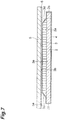
- Fig. 7 is a diagram illustrating an attachment step of attaching the supporting substrate 2 and the scintillator layer 3 to the light detection portion 5.
- Figs. 8(a) and 8(b) are diagrams illustrating a deformation step of deforming the supporting substrate 2 and the scintillator layer 3. Specifically, Fig. 8(a) illustrates the supporting substrate 2 and the scintillator layer 3 when the deformation step starts. Fig. 8(b) illustrates the supporting substrate 2 and the scintillator layer 3 when the deformation step ends.
- the scintillator layer 3 is formed on the principal surface 2a of the supporting substrate 2.
- the supporting substrate 2 is fixed to a reinforcing plate having a sufficient rigidity.
- Tl-doped CsI is vapor-deposited on the principal surface 2a in a state where the supporting substrate 2 and the reinforcing plate are rotated, whereby the scintillator layer 3 is formed.
- the scintillator layer 3 is formed in a region of the principal surface 2a of the supporting substrate 2 closer to the center. That is, a non-coated area on which the scintillator layer 3 is not formed is formed on the outer side of the principal surface 2a.
- a width N of the non-coated area illustrated in Fig. 5 is preferably small from the perspective of decreasing a constituent member and is preferably large from the perspective of improving assembling workability.
- the width N of the non-coated area may be in the range of 1 mm to 10 mm, for example.
- the non-coated area corresponds to a region that corresponds to the above-described opposing end portion 2c of the principal surface 2a.
- the scintillator layer 3 formed in the scintillator layer forming step has an approximately quadrangular pyramid shape such that the scintillator layer broadens as it advances from the emission surface 3b to the incident surface 3a.
- the scintillator layer 3 in this stage has such a structure that the area of the incident surface 3a is larger than the area of the emission surface 3b, and an inclined state of the side surface 3d is different from that of the side surface 3c of Fig. 1 .
- the side surface 3d protrudes outward as it advances from the emission surface 3b to the incident surface 3a.
- An inclination angle ⁇ between the side surface 3d and the emission surface 3b may be greater than 90° and smaller than 180°.
- the inclination angle ⁇ may be in the range of 100° to 175° and may be in the range of 135° to 175°.
- the moisture-proof protective film 4 is formed.
- the supporting substrate 2 on which the scintillator layer 3 is formed is input into a vapor deposition chamber of a chemical vapor deposition (CVD) apparatus.
- CVD chemical vapor deposition
- the moisture-proof protective film 4 is formed so as to cover the outer sides of the supporting substrate 2 and the scintillator layer 3.
- the supporting substrate 2 and the scintillator layer 3 have sufficient flexible properties in a state of being covered by the moisture-proof protective film 4.
- the supporting substrate 2 and the scintillator layer 3 that are covered by the moisture-proof protective film 4 are attached to the light detection portion 5.
- the adhesive layer 6 is formed on the light receiving surface 5a of the light detection portion 5.
- the supporting substrate 2 and the scintillator layer 3 are attached to the light detection portion 5 so that the emission surface 3b of the scintillator layer 3 faces the light receiving surface 5a of the light detection portion 5.
- the supporting substrate 2 and the scintillator layer 3 are deformed so as to extend along the light receiving surface 5a of the light detection portion 5.
- the supporting substrate 2 and the scintillator layer 3 having flexible properties are deformed by pressing the same toward the light detection portion 5. Due to the pressing, the supporting substrate 2 and the scintillator layer 3 are deformed from the state illustrated in Fig. 8(a) to the state illustrated in Fig. 8(b) .
- the supporting substrate 2 and the scintillator layer 3 are deformed so as to be closely attached along the light receiving surface 5a of the light detection portion 5.
- the side surface 3d is pressed against the light receiving surface 5a of the light detection portion 5 and is deformed to be the same surface as the emission surface 3b. At the same time, a portion of the incident surface 3a of the scintillator layer 3 is deformed to form the side surfaces 3c.
- the supporting substrate 2 is deformed from the flat plate shape illustrated in Fig. 8(a) into an approximately shallow dish shape illustrated in Fig. 8(b) . Due to this deformation, the outer edge portion 2b and the opposing end portion 2c are formed on the outer periphery side of the supporting substrate 2.
- the outer edge portion 2b is formed by being bent so as to extend along the side surface 3c in accordance with the forming of the side surface 3c of the scintillator layer 3.
- the outer edge portion 2b is inclined along the side surface 3c of the scintillator layer 3.
- the opposing end portion 2c is moved toward the light detection portion 5 in accordance with the forming of the outer edge portion 2b.
- the principal surface 2a (the above-described non-coated area) of the opposing end portion 2c and the adhesive layer 6 are attached through the moisture-proof protective film 4 interposed.
- the area of the non-coated area corresponds to the area of the opposing end portion 2c attached to the adhesive layer 6.
- the adhesive layer 6 is cured, and a predetermined finishing treatment is performed. In this way, the radiation detector 1 illustrated in Fig. 1 is obtained.
- the outer edge portion 2b of the supporting substrate 2 extends to reach the side surface 3c of the scintillator layer 3, and the outer periphery of the scintillator layer 3 is reinforced by the supporting substrate 2.
- the side surface 3c of the scintillator layer 3 is inclined toward the outer side as the side surface 3c advances from the incident surface 3a to the emission surface 3b.
- a flexible substrate made from a polymer film is used as the supporting substrate 2.
- the supporting substrate 2 and the scintillator layer 3 so as to conform to the shape of the light detection portion 5.
- the gap between the scintillator layer 3 and the light detection portion 5 can be decreased, it is possible to suppress deterioration of the resolution resulting from the gap between the scintillator layer 3 and the light detection portion 5.
- a flexible substrate is used as the supporting substrate 2, it is possible to form the outer edge portion 2b easily.
- the outer edge portion 2b of the supporting substrate 2 extends to reach the side surface 3c of the scintillator layer 3.
- the distance between the supporting substrate 2 and the light detection portion 5 is small as compared to a case where the supporting substrate 2 has a flat plate shape such that the supporting substrate 2 does not extend to reach the side surface 3c of the scintillator layer 3. Therefore, it is possible to attach the supporting substrate 2 and the light detection portion 5 with a small amount of the adhesive agent.
- the opposing end portion 2c is provided on the outer side of the outer edge portion 2b so as to face the light detection portion 5.
- the emission surface 3b of the scintillator layer 3 and the opposing end portion 2c of the supporting substrate 2 are attached to the light detection portion 5 by the adhesive layer 6. In this way, it is possible to fix the scintillator layer 3 and the supporting substrate 2 to the light detection portion 5 with a simple configuration.
- the moisture-proof protective film 4 is provided so as to cover the outer sides of the supporting substrate 2 and the scintillator layer 3, it is possible to suppress moisture from entering into the scintillator layer 3. Further, in the radiation detector 1, since the side surface 3c of the scintillator layer 3 is covered by the outer edge portion 2b of the supporting substrate 2, entering of moisture into the scintillator layer 3 is suppressed as compared to a case where the side surface 3c of the scintillator layer 3 is not covered by the supporting substrate 2. Therefore, according to the radiation detector 1, it is possible to prevent deterioration of the scintillator layer 3 due to entering moisture. This contributes to extending the lifespan of the radiation detector 1.
- the present invention is not limited to the above-described embodiment.
- the material of the supporting substrate 2 is not limited to a polymer film, and aluminum may be used.
- the side surface 3c of the scintillator layer 3 does not always have to be entirely covered by the supporting substrate 2, and only a portion may be covered. Further, the opposing end portion 2c of the supporting substrate 2 does not have to be attached to the adhesive layer 6. That is, the scintillator layer 3 is not limited to being sealed by the supporting substrate 2 and the adhesive layer 6, and a gap may be formed in a lateral side of the scintillator layer 3. Moreover, the flange-shaped opposing end portion 2c does not always have to be formed. Further, the moisture-proof protective film 4 does not always have to be formed.
- the present invention can be used in a radiation detector.
Landscapes
- Physics & Mathematics (AREA)
- Health & Medical Sciences (AREA)
- Life Sciences & Earth Sciences (AREA)
- General Physics & Mathematics (AREA)
- High Energy & Nuclear Physics (AREA)
- Molecular Biology (AREA)
- Spectroscopy & Molecular Physics (AREA)
- Chemical & Material Sciences (AREA)
- Crystallography & Structural Chemistry (AREA)
- Measurement Of Radiation (AREA)
- Apparatus For Radiation Diagnosis (AREA)
- Nuclear Medicine (AREA)
Claims (7)
- Procédé de fabrication d'un détecteur de rayonnement comportant :la mise à disposition d'un substrat de support flexible (2) à travers lequel peuvent être transmis des rayonnements;la formation d'une couche de scintillateur (3) sur une surface principale (2a) du substrat (2), la couche de scintillateur (3) comprenant une surface d'incidence (3a) sur laquelle un rayonnement est incident et une surface d'émission (3b) émettant de la lumière générée par le rayonnement incident et située sur un côté opposé à la surface d'incidence (3a) ; etl'agencement d'une partie de détection de lumière (5) côté surface d'émission de la couche de scintillateur (3) pour détecter de la lumière émise par la surface d'émission (3b),où une surface latérale (3c) de la couche de scintillateur (3) est inclinée vers l'extérieur à mesure que la surface latérale (3c) s'étend de la surface d'incidence (3a) à la surface d'émission (3b),le substrat (2) présente une partie de bord extérieur (2b) qui s'étend jusqu'à atteindre la surface latérale (3c) de la couche de scintillateur (3) et une périphérie extérieure de la couche de scintillateur (3) est renforcée par le substrat (2), etcaractérisé en ce que le substrat (2) et la couche de scintillateur (3) sont déformés en étant pressées vers la partie de détection de lumière (5).
- Procédé selon la revendication 1, où le substrat (2) est composé d'un film polymère.
- Procédé selon la revendication 1 ou 2, où le substrat (2) comporte une partie d'extrémité opposée (2c) formée sur un côté extérieur de la partie de bord extérieur (2b) de telle manière que la partie de bord extérieur (2b) fait face à la partie de détection de lumière (5).
- Procédé selon l'une quelconque des revendications 1 à 3, où le détecteur de rayonnement comporte en outre une couche adhésive (6) qui attache la couche de scintillateur (3) et le substrat (2) à la partie de détection de lumière (5).
- Procédé selon l'une quelconque des revendications 1 à 4, où le détecteur de rayonnement comporte en outre ;
un film protecteur résistant à l'humidité (4) couvrant des côtés extérieurs du substrat (2) et de la couche de scintillateur (3),
où le substrat (2) et la couche de scintillateur (3) sont attachés à la couche adhésive (6) par l'intermédiaire du film protecteur résistant à l'humidité (4). - Procédé selon l'une quelconque des revendications 1 à 5, où un angle entre la surface d'émission (3b) et la surface latérale (3c) de la couche de scintillateur (3) est compris entre 5° et 80°.
- Procédé selon la revendication 6, où l'angle entre la surface d'émission (3b) et la surface latérale (3c) de la couche de scintillateur (3) est compris entre 5° et 45°.
Applications Claiming Priority (2)
| Application Number | Priority Date | Filing Date | Title |
|---|---|---|---|
| JP2010187444A JP5649872B2 (ja) | 2010-08-24 | 2010-08-24 | 放射線検出器の製造方法 |
| PCT/JP2011/063972 WO2012026188A1 (fr) | 2010-08-24 | 2011-06-17 | Détecteur de rayonnement |
Publications (3)
| Publication Number | Publication Date |
|---|---|
| EP2610643A1 EP2610643A1 (fr) | 2013-07-03 |
| EP2610643A4 EP2610643A4 (fr) | 2016-11-09 |
| EP2610643B1 true EP2610643B1 (fr) | 2019-12-04 |
Family
ID=45723204
Family Applications (1)
| Application Number | Title | Priority Date | Filing Date |
|---|---|---|---|
| EP11819660.9A Active EP2610643B1 (fr) | 2010-08-24 | 2011-06-17 | Détecteur de rayonnement |
Country Status (6)
| Country | Link |
|---|---|
| US (2) | US8890078B2 (fr) |
| EP (1) | EP2610643B1 (fr) |
| JP (1) | JP5649872B2 (fr) |
| KR (1) | KR101780522B1 (fr) |
| CN (1) | CN102971643B (fr) |
| WO (1) | WO2012026188A1 (fr) |
Families Citing this family (19)
| Publication number | Priority date | Publication date | Assignee | Title |
|---|---|---|---|---|
| JP5686993B2 (ja) * | 2010-06-04 | 2015-03-18 | 浜松ホトニクス株式会社 | シンチレータパネル及び放射線イメージセンサ |
| KR101352492B1 (ko) * | 2012-04-02 | 2014-01-17 | 아스텔 주식회사 | 엑스레이 디텍터 및 이의 제조방법 |
| JP6169922B2 (ja) * | 2012-08-29 | 2017-07-26 | 東芝メディカルシステムズ株式会社 | X線検出サブモジュール、x線検出モジュールおよびx線ct装置 |
| JP6324045B2 (ja) * | 2013-12-04 | 2018-05-16 | 三菱電機株式会社 | 表示装置 |
| JP2016038279A (ja) * | 2014-08-07 | 2016-03-22 | コニカミノルタ株式会社 | シンチレータパネルおよびこれを備えた放射線検出器 |
| JP6435154B2 (ja) * | 2014-10-14 | 2018-12-05 | 株式会社ジョブ | 光子計数型検出器 |
| JP5970641B2 (ja) * | 2014-12-09 | 2016-08-17 | 雫石 誠 | 撮像装置 |
| DE102014225396B3 (de) * | 2014-12-10 | 2016-04-28 | Siemens Aktiengesellschaft | Sensorboard für ein Detektormodul und Verfahren zu dessen Herstellung |
| JP2016128779A (ja) * | 2015-01-09 | 2016-07-14 | 株式会社東芝 | 放射線検出器及びその製造方法 |
| JP6487263B2 (ja) * | 2015-04-20 | 2019-03-20 | 浜松ホトニクス株式会社 | 放射線検出器及びその製造方法 |
| JP6799917B2 (ja) * | 2015-12-21 | 2020-12-16 | 浜松ホトニクス株式会社 | 放射線検出装置、放射線検査システム、及び、放射線検出装置の調整方法 |
| JP6646002B2 (ja) * | 2017-03-22 | 2020-02-14 | 富士フイルム株式会社 | 放射線検出器及び放射線画像撮影装置 |
| JP6707130B2 (ja) * | 2017-03-22 | 2020-06-10 | 富士フイルム株式会社 | 放射線検出器及び放射線画像撮影装置 |
| JP6862324B2 (ja) | 2017-09-27 | 2021-04-21 | 浜松ホトニクス株式会社 | シンチレータパネル及び放射線検出器 |
| CN109659385A (zh) * | 2017-10-10 | 2019-04-19 | 群创光电股份有限公司 | 感测装置 |
| JP2019070605A (ja) * | 2017-10-11 | 2019-05-09 | キヤノン電子管デバイス株式会社 | 放射線検出モジュール、シンチレータパネル、および放射線検出器 |
| KR101986503B1 (ko) | 2017-10-31 | 2019-06-10 | 주식회사 엠원인터내셔널 | 해양환경 방사선 측정 및 분석 시스템 |
| JP7325295B2 (ja) * | 2019-10-24 | 2023-08-14 | 浜松ホトニクス株式会社 | シンチレータパネル、放射線検出器、シンチレータパネルの製造方法、及び、放射線検出器の製造方法 |
| KR102900082B1 (ko) * | 2023-10-16 | 2025-12-16 | 주식회사 듀오픽스레이 | 엑스선 섬광체를 갖는 엑스레이 디텍터 |
Family Cites Families (13)
| Publication number | Priority date | Publication date | Assignee | Title |
|---|---|---|---|---|
| CN101285888B (zh) * | 1997-02-14 | 2012-01-18 | 浜松光子学株式会社 | 放射线检测元件及其制造方法 |
| JP3405706B2 (ja) * | 1997-02-14 | 2003-05-12 | 浜松ホトニクス株式会社 | 放射線検出素子 |
| JP2004061115A (ja) | 2002-07-24 | 2004-02-26 | Canon Inc | シンチレーターパネル、放射線検出装置及び放射線撮像システム |
| JP2007057428A (ja) * | 2005-08-25 | 2007-03-08 | Canon Inc | 放射線検出装置及び放射線撮像システム |
| JP5089195B2 (ja) | 2006-03-02 | 2012-12-05 | キヤノン株式会社 | 放射線検出装置、シンチレータパネル、放射線検出システム及び放射線検出装置の製造方法 |
| JP2007240306A (ja) * | 2006-03-08 | 2007-09-20 | Toshiba Corp | シンチレータパネルおよび平面検出器 |
| WO2008018277A1 (fr) | 2006-08-08 | 2008-02-14 | Konica Minolta Medical & Graphic, Inc. | DÉTECTEUR de panneau plat |
| WO2008117821A1 (fr) * | 2007-03-27 | 2008-10-02 | Kabushiki Kaisha Toshiba | Panneau scintillant et détecteur de rayonnement |
| JP5004848B2 (ja) * | 2007-04-18 | 2012-08-22 | キヤノン株式会社 | 放射線検出装置及び放射線検出システム |
| US7732788B2 (en) * | 2007-10-23 | 2010-06-08 | Hamamatsu Photonics K.K. | Radiation image converting panel, scintillator panel and radiation image sensor |
| JP5022805B2 (ja) * | 2007-07-26 | 2012-09-12 | 東芝電子管デバイス株式会社 | 放射線検出器 |
| US8525132B2 (en) * | 2007-09-06 | 2013-09-03 | Konica Minolta Medical & Graphic, Inc. | Flat panel detector |
| JP2009068888A (ja) * | 2007-09-11 | 2009-04-02 | Konica Minolta Medical & Graphic Inc | フラットパネルディテクタ |
-
2010
- 2010-08-24 JP JP2010187444A patent/JP5649872B2/ja active Active
-
2011
- 2011-06-17 CN CN201180032860.8A patent/CN102971643B/zh active Active
- 2011-06-17 EP EP11819660.9A patent/EP2610643B1/fr active Active
- 2011-06-17 KR KR1020137002709A patent/KR101780522B1/ko active Active
- 2011-06-17 WO PCT/JP2011/063972 patent/WO2012026188A1/fr not_active Ceased
- 2011-06-17 US US13/810,254 patent/US8890078B2/en active Active
-
2014
- 2014-10-17 US US14/517,336 patent/US9146325B2/en active Active
Non-Patent Citations (1)
| Title |
|---|
| None * |
Also Published As
| Publication number | Publication date |
|---|---|
| US20150059151A1 (en) | 2015-03-05 |
| KR20130106349A (ko) | 2013-09-27 |
| EP2610643A4 (fr) | 2016-11-09 |
| CN102971643A (zh) | 2013-03-13 |
| US20130112882A1 (en) | 2013-05-09 |
| KR101780522B1 (ko) | 2017-09-21 |
| JP2012047486A (ja) | 2012-03-08 |
| EP2610643A1 (fr) | 2013-07-03 |
| WO2012026188A1 (fr) | 2012-03-01 |
| US8890078B2 (en) | 2014-11-18 |
| US9146325B2 (en) | 2015-09-29 |
| JP5649872B2 (ja) | 2015-01-07 |
| CN102971643B (zh) | 2015-09-23 |
Similar Documents
| Publication | Publication Date | Title |
|---|---|---|
| US9146325B2 (en) | Method for detecting radiation | |
| US9158010B2 (en) | Radiation detector | |
| EP3004930B1 (fr) | Structure de protection contre l'humidité pour dispositif et son procédé de fabrication | |
| EP3438705B1 (fr) | Détecteur de rayonnement et panneau de scintillateur | |
| US10983225B2 (en) | Radiation detector manufacturing method | |
| CN116635751B (zh) | 放射线检测器、放射线检测器的制造方法和闪烁体面板组件 | |
| US9513383B1 (en) | Scintillator sealing with foil | |
| JP7268454B2 (ja) | 放射線撮影装置 | |
| EP3770923B1 (fr) | Détecteur de rayonnement | |
| JP2015155799A (ja) | シンチレータ、放射線検出装置、放射線検出装置の製造方法及び放射線検出システム | |
| KR20160021387A (ko) | 신틸레이터 패널 및 그 제조방법 | |
| US11953631B2 (en) | Scintillator panel, and radiation detector | |
| EP3896705A1 (fr) | Module de scintillateur, unité de capteur de scintillateur et procédé de fabrication | |
| US20240045085A1 (en) | Radiation detector, radiation detector manufacturing method, and scintillator panel unit |
Legal Events
| Date | Code | Title | Description |
|---|---|---|---|
| PUAI | Public reference made under article 153(3) epc to a published international application that has entered the european phase |
Free format text: ORIGINAL CODE: 0009012 |
|
| 17P | Request for examination filed |
Effective date: 20130225 |
|
| AK | Designated contracting states |
Kind code of ref document: A1 Designated state(s): AL AT BE BG CH CY CZ DE DK EE ES FI FR GB GR HR HU IE IS IT LI LT LU LV MC MK MT NL NO PL PT RO RS SE SI SK SM TR |
|
| DAX | Request for extension of the european patent (deleted) | ||
| REG | Reference to a national code |
Ref country code: DE Ref legal event code: R079 Ref document number: 602011063823 Country of ref document: DE Free format text: PREVIOUS MAIN CLASS: G01T0001200000 Ipc: G01T0001202000 |
|
| RA4 | Supplementary search report drawn up and despatched (corrected) |
Effective date: 20161007 |
|
| RIC1 | Information provided on ipc code assigned before grant |
Ipc: G01T 1/161 20060101ALI20161003BHEP Ipc: A61B 6/03 20060101ALI20161003BHEP Ipc: G01T 1/202 20060101AFI20161003BHEP Ipc: A61B 6/00 20060101ALI20161003BHEP |
|
| STAA | Information on the status of an ep patent application or granted ep patent |
Free format text: STATUS: EXAMINATION IS IN PROGRESS |
|
| 17Q | First examination report despatched |
Effective date: 20180605 |
|
| GRAP | Despatch of communication of intention to grant a patent |
Free format text: ORIGINAL CODE: EPIDOSNIGR1 |
|
| STAA | Information on the status of an ep patent application or granted ep patent |
Free format text: STATUS: GRANT OF PATENT IS INTENDED |
|
| RIN1 | Information on inventor provided before grant (corrected) |
Inventor name: KUSUYAMA, YUTAKA Inventor name: YAMASHITA, MASANORI Inventor name: TOYAMA, SHINTARO Inventor name: OSAWA, HIROTAKE Inventor name: SHIKIDA, MUNENORI |
|
| INTG | Intention to grant announced |
Effective date: 20190708 |
|
| GRAS | Grant fee paid |
Free format text: ORIGINAL CODE: EPIDOSNIGR3 |
|
| GRAA | (expected) grant |
Free format text: ORIGINAL CODE: 0009210 |
|
| STAA | Information on the status of an ep patent application or granted ep patent |
Free format text: STATUS: THE PATENT HAS BEEN GRANTED |
|
| AK | Designated contracting states |
Kind code of ref document: B1 Designated state(s): AL AT BE BG CH CY CZ DE DK EE ES FI FR GB GR HR HU IE IS IT LI LT LU LV MC MK MT NL NO PL PT RO RS SE SI SK SM TR |
|
| REG | Reference to a national code |
Ref country code: GB Ref legal event code: FG4D |
|
| REG | Reference to a national code |
Ref country code: CH Ref legal event code: EP |
|
| REG | Reference to a national code |
Ref country code: AT Ref legal event code: REF Ref document number: 1210078 Country of ref document: AT Kind code of ref document: T Effective date: 20191215 |
|
| REG | Reference to a national code |
Ref country code: DE Ref legal event code: R096 Ref document number: 602011063823 Country of ref document: DE |
|
| REG | Reference to a national code |
Ref country code: IE Ref legal event code: FG4D |
|
| REG | Reference to a national code |
Ref country code: FI Ref legal event code: FGE |
|
| REG | Reference to a national code |
Ref country code: LT Ref legal event code: MG4D |
|
| PG25 | Lapsed in a contracting state [announced via postgrant information from national office to epo] |
Ref country code: GR Free format text: LAPSE BECAUSE OF FAILURE TO SUBMIT A TRANSLATION OF THE DESCRIPTION OR TO PAY THE FEE WITHIN THE PRESCRIBED TIME-LIMIT Effective date: 20200305 Ref country code: NO Free format text: LAPSE BECAUSE OF FAILURE TO SUBMIT A TRANSLATION OF THE DESCRIPTION OR TO PAY THE FEE WITHIN THE PRESCRIBED TIME-LIMIT Effective date: 20200304 Ref country code: SE Free format text: LAPSE BECAUSE OF FAILURE TO SUBMIT A TRANSLATION OF THE DESCRIPTION OR TO PAY THE FEE WITHIN THE PRESCRIBED TIME-LIMIT Effective date: 20191204 Ref country code: LV Free format text: LAPSE BECAUSE OF FAILURE TO SUBMIT A TRANSLATION OF THE DESCRIPTION OR TO PAY THE FEE WITHIN THE PRESCRIBED TIME-LIMIT Effective date: 20191204 Ref country code: BG Free format text: LAPSE BECAUSE OF FAILURE TO SUBMIT A TRANSLATION OF THE DESCRIPTION OR TO PAY THE FEE WITHIN THE PRESCRIBED TIME-LIMIT Effective date: 20200304 Ref country code: ES Free format text: LAPSE BECAUSE OF FAILURE TO SUBMIT A TRANSLATION OF THE DESCRIPTION OR TO PAY THE FEE WITHIN THE PRESCRIBED TIME-LIMIT Effective date: 20191204 Ref country code: LT Free format text: LAPSE BECAUSE OF FAILURE TO SUBMIT A TRANSLATION OF THE DESCRIPTION OR TO PAY THE FEE WITHIN THE PRESCRIBED TIME-LIMIT Effective date: 20191204 |
|
| REG | Reference to a national code |
Ref country code: NL Ref legal event code: FP |
|
| PG25 | Lapsed in a contracting state [announced via postgrant information from national office to epo] |
Ref country code: HR Free format text: LAPSE BECAUSE OF FAILURE TO SUBMIT A TRANSLATION OF THE DESCRIPTION OR TO PAY THE FEE WITHIN THE PRESCRIBED TIME-LIMIT Effective date: 20191204 Ref country code: RS Free format text: LAPSE BECAUSE OF FAILURE TO SUBMIT A TRANSLATION OF THE DESCRIPTION OR TO PAY THE FEE WITHIN THE PRESCRIBED TIME-LIMIT Effective date: 20191204 |
|
| PG25 | Lapsed in a contracting state [announced via postgrant information from national office to epo] |
Ref country code: AL Free format text: LAPSE BECAUSE OF FAILURE TO SUBMIT A TRANSLATION OF THE DESCRIPTION OR TO PAY THE FEE WITHIN THE PRESCRIBED TIME-LIMIT Effective date: 20191204 |
|
| PG25 | Lapsed in a contracting state [announced via postgrant information from national office to epo] |
Ref country code: PT Free format text: LAPSE BECAUSE OF FAILURE TO SUBMIT A TRANSLATION OF THE DESCRIPTION OR TO PAY THE FEE WITHIN THE PRESCRIBED TIME-LIMIT Effective date: 20200429 Ref country code: CZ Free format text: LAPSE BECAUSE OF FAILURE TO SUBMIT A TRANSLATION OF THE DESCRIPTION OR TO PAY THE FEE WITHIN THE PRESCRIBED TIME-LIMIT Effective date: 20191204 Ref country code: RO Free format text: LAPSE BECAUSE OF FAILURE TO SUBMIT A TRANSLATION OF THE DESCRIPTION OR TO PAY THE FEE WITHIN THE PRESCRIBED TIME-LIMIT Effective date: 20191204 Ref country code: EE Free format text: LAPSE BECAUSE OF FAILURE TO SUBMIT A TRANSLATION OF THE DESCRIPTION OR TO PAY THE FEE WITHIN THE PRESCRIBED TIME-LIMIT Effective date: 20191204 |
|
| PG25 | Lapsed in a contracting state [announced via postgrant information from national office to epo] |
Ref country code: SM Free format text: LAPSE BECAUSE OF FAILURE TO SUBMIT A TRANSLATION OF THE DESCRIPTION OR TO PAY THE FEE WITHIN THE PRESCRIBED TIME-LIMIT Effective date: 20191204 Ref country code: IS Free format text: LAPSE BECAUSE OF FAILURE TO SUBMIT A TRANSLATION OF THE DESCRIPTION OR TO PAY THE FEE WITHIN THE PRESCRIBED TIME-LIMIT Effective date: 20200404 Ref country code: SK Free format text: LAPSE BECAUSE OF FAILURE TO SUBMIT A TRANSLATION OF THE DESCRIPTION OR TO PAY THE FEE WITHIN THE PRESCRIBED TIME-LIMIT Effective date: 20191204 |
|
| REG | Reference to a national code |
Ref country code: DE Ref legal event code: R097 Ref document number: 602011063823 Country of ref document: DE |
|
| REG | Reference to a national code |
Ref country code: AT Ref legal event code: MK05 Ref document number: 1210078 Country of ref document: AT Kind code of ref document: T Effective date: 20191204 |
|
| PLBE | No opposition filed within time limit |
Free format text: ORIGINAL CODE: 0009261 |
|
| STAA | Information on the status of an ep patent application or granted ep patent |
Free format text: STATUS: NO OPPOSITION FILED WITHIN TIME LIMIT |
|
| PG25 | Lapsed in a contracting state [announced via postgrant information from national office to epo] |
Ref country code: DK Free format text: LAPSE BECAUSE OF FAILURE TO SUBMIT A TRANSLATION OF THE DESCRIPTION OR TO PAY THE FEE WITHIN THE PRESCRIBED TIME-LIMIT Effective date: 20191204 |
|
| 26N | No opposition filed |
Effective date: 20200907 |
|
| PG25 | Lapsed in a contracting state [announced via postgrant information from national office to epo] |
Ref country code: AT Free format text: LAPSE BECAUSE OF FAILURE TO SUBMIT A TRANSLATION OF THE DESCRIPTION OR TO PAY THE FEE WITHIN THE PRESCRIBED TIME-LIMIT Effective date: 20191204 Ref country code: SI Free format text: LAPSE BECAUSE OF FAILURE TO SUBMIT A TRANSLATION OF THE DESCRIPTION OR TO PAY THE FEE WITHIN THE PRESCRIBED TIME-LIMIT Effective date: 20191204 Ref country code: PL Free format text: LAPSE BECAUSE OF FAILURE TO SUBMIT A TRANSLATION OF THE DESCRIPTION OR TO PAY THE FEE WITHIN THE PRESCRIBED TIME-LIMIT Effective date: 20191204 |
|
| PG25 | Lapsed in a contracting state [announced via postgrant information from national office to epo] |
Ref country code: IT Free format text: LAPSE BECAUSE OF FAILURE TO SUBMIT A TRANSLATION OF THE DESCRIPTION OR TO PAY THE FEE WITHIN THE PRESCRIBED TIME-LIMIT Effective date: 20191204 Ref country code: MC Free format text: LAPSE BECAUSE OF FAILURE TO SUBMIT A TRANSLATION OF THE DESCRIPTION OR TO PAY THE FEE WITHIN THE PRESCRIBED TIME-LIMIT Effective date: 20191204 |
|
| REG | Reference to a national code |
Ref country code: CH Ref legal event code: PL |
|
| PG25 | Lapsed in a contracting state [announced via postgrant information from national office to epo] |
Ref country code: LU Free format text: LAPSE BECAUSE OF NON-PAYMENT OF DUE FEES Effective date: 20200617 |
|
| REG | Reference to a national code |
Ref country code: BE Ref legal event code: MM Effective date: 20200630 |
|
| PG25 | Lapsed in a contracting state [announced via postgrant information from national office to epo] |
Ref country code: CH Free format text: LAPSE BECAUSE OF NON-PAYMENT OF DUE FEES Effective date: 20200630 Ref country code: IE Free format text: LAPSE BECAUSE OF NON-PAYMENT OF DUE FEES Effective date: 20200617 Ref country code: LI Free format text: LAPSE BECAUSE OF NON-PAYMENT OF DUE FEES Effective date: 20200630 |
|
| PG25 | Lapsed in a contracting state [announced via postgrant information from national office to epo] |
Ref country code: BE Free format text: LAPSE BECAUSE OF NON-PAYMENT OF DUE FEES Effective date: 20200630 |
|
| PG25 | Lapsed in a contracting state [announced via postgrant information from national office to epo] |
Ref country code: TR Free format text: LAPSE BECAUSE OF FAILURE TO SUBMIT A TRANSLATION OF THE DESCRIPTION OR TO PAY THE FEE WITHIN THE PRESCRIBED TIME-LIMIT Effective date: 20191204 Ref country code: MT Free format text: LAPSE BECAUSE OF FAILURE TO SUBMIT A TRANSLATION OF THE DESCRIPTION OR TO PAY THE FEE WITHIN THE PRESCRIBED TIME-LIMIT Effective date: 20191204 Ref country code: CY Free format text: LAPSE BECAUSE OF FAILURE TO SUBMIT A TRANSLATION OF THE DESCRIPTION OR TO PAY THE FEE WITHIN THE PRESCRIBED TIME-LIMIT Effective date: 20191204 |
|
| PG25 | Lapsed in a contracting state [announced via postgrant information from national office to epo] |
Ref country code: MK Free format text: LAPSE BECAUSE OF FAILURE TO SUBMIT A TRANSLATION OF THE DESCRIPTION OR TO PAY THE FEE WITHIN THE PRESCRIBED TIME-LIMIT Effective date: 20191204 |
|
| P01 | Opt-out of the competence of the unified patent court (upc) registered |
Effective date: 20230509 |
|
| PGFP | Annual fee paid to national office [announced via postgrant information from national office to epo] |
Ref country code: NL Payment date: 20250516 Year of fee payment: 15 |
|
| PGFP | Annual fee paid to national office [announced via postgrant information from national office to epo] |
Ref country code: FI Payment date: 20250620 Year of fee payment: 15 |
|
| PGFP | Annual fee paid to national office [announced via postgrant information from national office to epo] |
Ref country code: DE Payment date: 20250429 Year of fee payment: 15 |
|
| PGFP | Annual fee paid to national office [announced via postgrant information from national office to epo] |
Ref country code: GB Payment date: 20250501 Year of fee payment: 15 |
|
| PGFP | Annual fee paid to national office [announced via postgrant information from national office to epo] |
Ref country code: FR Payment date: 20250508 Year of fee payment: 15 |