EP2608263A2 - Tunnel-Feldeffekt-Transistor und Verfahren zur Herstellung davon - Google Patents
Tunnel-Feldeffekt-Transistor und Verfahren zur Herstellung davon Download PDFInfo
- Publication number
- EP2608263A2 EP2608263A2 EP12198391.0A EP12198391A EP2608263A2 EP 2608263 A2 EP2608263 A2 EP 2608263A2 EP 12198391 A EP12198391 A EP 12198391A EP 2608263 A2 EP2608263 A2 EP 2608263A2
- Authority
- EP
- European Patent Office
- Prior art keywords
- channel
- source
- layer
- interface
- metal
- Prior art date
- Legal status (The legal status is an assumption and is not a legal conclusion. Google has not performed a legal analysis and makes no representation as to the accuracy of the status listed.)
- Withdrawn
Links
Images




Classifications
-
- H—ELECTRICITY
- H10—SEMICONDUCTOR DEVICES; ELECTRIC SOLID-STATE DEVICES NOT OTHERWISE PROVIDED FOR
- H10D—INORGANIC ELECTRIC SEMICONDUCTOR DEVICES
- H10D62/00—Semiconductor bodies, or regions thereof, of devices having potential barriers
- H10D62/10—Shapes, relative sizes or dispositions of the regions of the semiconductor bodies; Shapes of the semiconductor bodies
- H10D62/13—Semiconductor regions connected to electrodes carrying current to be rectified, amplified or switched, e.g. source or drain regions
- H10D62/141—Anode or cathode regions of thyristors; Collector or emitter regions of gated bipolar-mode devices, e.g. of IGBTs
-
- H—ELECTRICITY
- H10—SEMICONDUCTOR DEVICES; ELECTRIC SOLID-STATE DEVICES NOT OTHERWISE PROVIDED FOR
- H10D—INORGANIC ELECTRIC SEMICONDUCTOR DEVICES
- H10D30/00—Field-effect transistors [FET]
- H10D30/60—Insulated-gate field-effect transistors [IGFET]
-
- H—ELECTRICITY
- H10—SEMICONDUCTOR DEVICES; ELECTRIC SOLID-STATE DEVICES NOT OTHERWISE PROVIDED FOR
- H10D—INORGANIC ELECTRIC SEMICONDUCTOR DEVICES
- H10D12/00—Bipolar devices controlled by the field effect, e.g. insulated-gate bipolar transistors [IGBT]
- H10D12/01—Manufacture or treatment
- H10D12/021—Manufacture or treatment of gated diodes, e.g. field-controlled diodes [FCD]
-
- H—ELECTRICITY
- H10—SEMICONDUCTOR DEVICES; ELECTRIC SOLID-STATE DEVICES NOT OTHERWISE PROVIDED FOR
- H10D—INORGANIC ELECTRIC SEMICONDUCTOR DEVICES
- H10D12/00—Bipolar devices controlled by the field effect, e.g. insulated-gate bipolar transistors [IGBT]
- H10D12/211—Gated diodes
-
- H—ELECTRICITY
- H10—SEMICONDUCTOR DEVICES; ELECTRIC SOLID-STATE DEVICES NOT OTHERWISE PROVIDED FOR
- H10D—INORGANIC ELECTRIC SEMICONDUCTOR DEVICES
- H10D62/00—Semiconductor bodies, or regions thereof, of devices having potential barriers
- H10D62/10—Shapes, relative sizes or dispositions of the regions of the semiconductor bodies; Shapes of the semiconductor bodies
- H10D62/124—Shapes, relative sizes or dispositions of the regions of semiconductor bodies or of junctions between the regions
-
- H—ELECTRICITY
- H10—SEMICONDUCTOR DEVICES; ELECTRIC SOLID-STATE DEVICES NOT OTHERWISE PROVIDED FOR
- H10D—INORGANIC ELECTRIC SEMICONDUCTOR DEVICES
- H10D62/00—Semiconductor bodies, or regions thereof, of devices having potential barriers
- H10D62/10—Shapes, relative sizes or dispositions of the regions of the semiconductor bodies; Shapes of the semiconductor bodies
- H10D62/17—Semiconductor regions connected to electrodes not carrying current to be rectified, amplified or switched, e.g. channel regions
- H10D62/213—Channel regions of field-effect devices
-
- H—ELECTRICITY
- H10—SEMICONDUCTOR DEVICES; ELECTRIC SOLID-STATE DEVICES NOT OTHERWISE PROVIDED FOR
- H10D—INORGANIC ELECTRIC SEMICONDUCTOR DEVICES
- H10D62/00—Semiconductor bodies, or regions thereof, of devices having potential barriers
- H10D62/40—Crystalline structures
- H10D62/405—Orientations of crystalline planes
-
- H—ELECTRICITY
- H10—SEMICONDUCTOR DEVICES; ELECTRIC SOLID-STATE DEVICES NOT OTHERWISE PROVIDED FOR
- H10D—INORGANIC ELECTRIC SEMICONDUCTOR DEVICES
- H10D62/00—Semiconductor bodies, or regions thereof, of devices having potential barriers
- H10D62/60—Impurity distributions or concentrations
-
- H—ELECTRICITY
- H10—SEMICONDUCTOR DEVICES; ELECTRIC SOLID-STATE DEVICES NOT OTHERWISE PROVIDED FOR
- H10P—GENERIC PROCESSES OR APPARATUS FOR THE MANUFACTURE OR TREATMENT OF DEVICES COVERED BY CLASS H10
- H10P95/00—Generic processes or apparatus for manufacture or treatments not covered by the other groups of this subclass
Definitions
- the present invention relates to tunnel field effect transistors (TFET) where the drive current of the transistor is based on band-to-band tunnelling. Furthermore the invention relates to a method for manufacturing such tunnel field effect transistors.
- TFET tunnel field effect transistors
- Nanoelectronic devices being electronic devices comprising features with a dimension below 1 ⁇ m, e.g. a dimension between 1 nm and 500 nm, such as a dimension between 3 nm and 300 nm, are generally fabricated using semiconductor materials and processing for manufacturing the integrated circuits.
- a complementary metal-oxide-semiconductor (CMOS) field effect transistor is one of the core elements of the integrated circuits. Dimensions and operating voltages of CMOS transistors are continuously reduced, or scaled down, to obtain ever-higher performance and packaging density of the integrated circuits.
- CMOS complementary metal-oxide-semiconductor
- CMOS transistors One of the problems due to the scaling down of CMOS transistors is that the power consumption keeps increasing. This increase is partly because leakage currents are increasing, e.g. due to short channel effects, and partly because it becomes difficult to further decrease the power supply voltage. As the physical subthreshold swing for CMOS transistors is limited to about 60 mV/decade, a minimal power supply voltage will be needed to switch the transistor from the OFF state to the ON state.
- Tunnel field-effect transistors are typically advertised as successors of metal-oxide semiconductor field-effect transistors (MOSFETs), because of their absence of short-channel effects and because of their resulting low off-currents.
- MOSFETs metal-oxide semiconductor field-effect transistors
- Another advantage of TFETs is that their theoretical subthreshold swing can be less than 60 mV/dec, the physical limit of conventional MOSFETs, thereby offering the potential of operating at lower supply voltages compared to CMOS transistors.
- homostructure TFETs typically suffer from either low on-currents, such as e.g. all-silicon TFETs, i.e. with channel and source/drain regions formed in silicon, in which case this drawback is related to the large resistance of the larger tunnel barrier of silicon, or they suffer from high off-currents, such as e.g. all-indiumarsenide TFETs, i.e. with channel and source/drain regions formed in indiumarsenide, in which case this drawback is related to the low resistance of the tunnel barrier at the drain contact at which location an ambipolar current is generated.
- Heterostructure TFETs i.e.
- TFET tunnel Field Effect transistor
- Such TFET may have an average subthreshold swing below 60 mV/dec corresponding to a high on-current I on and/or a low off-current I off , even at reduced power supply voltage.
- the on-current I on may be above 100 micro-ampere/micrometer ( ⁇ A/ ⁇ m) while the off-current I off may be below 1 nano-ampere/micrometer (nA/ ⁇ m).
- the supply voltage may be 1 V or less
- TFET devices such as for example: vertical or horizontal TFETs, homo- or heterostructure TFETs, NanoWire-based TFET devices (NW-TFETs),...
- tunnel Field Effect transistor TFET
- Such tunnel TFETs may for instance be TFETs with a subthreshold swing below 60 mV/dec, a high on-current I on and low off-current I off even at reduced power supply voltage, e.g. 1 V or less.
- the present invention provides a tunnel Field Effect Transistor (TFET) comprising an interface between a source and a channel.
- TFET tunnel Field Effect Transistor
- a layer of a first crystalline semiconductor material is present which is substantially uniformly doped with a metal at a doping level close to, e.g. substantially equal to, such as equal to, but anyway lower than the solubility level of the metal in the first crystalline material.
- a layer of this first crystalline semiconductor material doped with this metal is present, the concentration of the metal decreasing with increasing distance from the interface. Provided the profile is steep, hence the decrease of the concentration with distance goes fast, there is a steep subthreshold swing.
- a high doping level, close to the solubility level of the metal in the first crystalline material results in a high on-current.
- a low off-current may be obtained by properly manufacturing the drain region.
- the source side interface layer may be further substantially uniformly doped with another dopant at a first concentration level and the channel side interface layer may be doped with this another dopant, the concentration thereof decreasing from this first concentration level with increasing distance from the interface.
- the another dopant for p-type dopants may be selected from the group of B, Al, Ga, In, Tl, Pd, Na, Be, Zn, Au, Co, V, Ni, MO, Hg, Sr, Ge, Cu, K, Sn, W, Pb, O, Fe, and for n-type dopants may be selected from the group of Li, Sb, P, As, Bi, Te, Ti, C, Mg, Se, Cr, Ta, Cs, Ba, S, Mn, Ag, Cd, Pt.
- the source side interface layer may have a thickness between 5 nm and 100 nm and the concentration level of the metal and/or the another dopant may be at least 1e19/cm 3 .
- the channel side interface layer may have a thickness between 5 nm to 100 nm and a concentration gradient between 10 nm/dec to 1 nm/dec.
- the thickness of the channel side interface layer should be at least such that the layer is not fully depleted in the gate-voltage range of interest. Hence the thickness depends on the obtained doping, which in turn is limited by the solubility limit of the dopant in the semiconductor material: the higher the doping, the thinner the layer can be.
- the interface may be in a plane, for example a ⁇ 111 ⁇ plane. If the interface is not in a plane, it may be formed by a set of planes which all are ⁇ 111 ⁇ planes.
- the source may protrude towards and into the channel.
- Such structure results in an increased tunneling region and as such also in a higher on-current I on .
- the transistor according to embodiments of the present invention may be a vertical type tunnel field effect transistor or a horizontal type tunnel field effect transistor.
- the first crystalline semiconductor material from which at least source and channel are formed may be the semiconductor material of a semiconductor-on-insulator substrate.
- the channel may further comprise a layer of a second crystalline semiconductor material adjacent to the channel side of the first crystalline semiconductor material and possibly adjacent to the channel side of the interface layer.
- the source may further comprise a layer of an alloy of the first crystalline semiconductor material and the metal, the alloy layer contacting the source side interface layer.
- the first crystalline semiconductor material may for example be Si x Ge 1-x with 0 ⁇ x ⁇ 1.
- the metal may for example be Aluminum.
- Aluminum is particularly advantageous as it forms a eutectic system with both silicon and germanium. This eutectic property is required to get the crystalline layer at the pyramidal sidewall.
- a second aspect of the present invention is related to a method for manufacturing a tunnel field effect transistor (TFET).
- TFET tunnel field effect transistor
- a method according to embodiments of the present invention may comprise providing a drain region in a semiconductor substrate, providing a channel region in the semiconductor substrate in contact with the drain region thereby forming a drain-channel interface with the drain region, providing a source region in contact with the channel region thereby forming a source-channel interface with the source region having a highly doped source-channel interface, e.g. with a dopant level of 1e19 at/cm 3 or higher.
- the source region may locally protrude into the channel region.
- the source region may locally have a tip-shaped protrusion into the channel region.
- Providing the source region may comprise providing a metal layer in contact with the channel region offset from the drain-channel interface, forming from the metal layer and from part of the semiconductor channel region in contact with the metal, a metal-semiconductor alloy, for example protruding into the channel region thereby forming a shaped source-channel interface having at least one tip along the source-channel interface.
- the metal-semiconductor alloy comprises metal material from the deposited metal layer and semiconductor material from the channel region and further also comprises a highly doped, e.g. at a doping level of 1e19 at/cm 3 or higher, shaped semiconductor layer at the shaped source-channel interface.
- the layer of metal may comprise another dopant.
- the method may comprise, when forming the source side interface layer and the channel side interface layer, doping these interface layers with this another dopant such that the source side interface layer is substantially uniformly doped with this another dopant at a first concentration level and the channel side interface layer is doped with this another dopant, the concentration thereof decreasing from the first concentration level with increasing distance from the interface.
- the another dopant may be, for p-type dopants, selected from the group of B, Al, Ga, In, Tl, Pd, Na, Be, Zn, Au, Co, V, Ni, MO, Hg, Sr, Ge, Cu, K, Sn, W, Pb, O, Fe, and for n-type dopants, selected from the group of Li, Sb, P, As, Bi, Te, Ti, C, Mg, Se, Cr, Ta, Cs, Ba, S, Mn, Ag, Cd, Pt.
- p-type dopants selected from the group of B, Al, Ga, In, Tl, Pd, Na, Be, Zn, Au, Co, V, Ni, MO, Hg, Sr, Ge, Cu, K, Sn, W, Pb, O, Fe, and for n-type dopants, selected from the group of Li, Sb, P, As, Bi, Te, Ti, C, Mg, Se, Cr, Ta, Cs, Ba, S, M
- the thickness of the interface layers is typically between and including 100 nm to 5 nm, for example between and including 15 nm and 5 nm.
- the interface layer at the source side of the interface may have a dopant concentration (of both metal and another dopant together) at least higher than 1e19/cm 3 , for example higher than 1e20/cm 3 .
- the interface layer at the channel side of the interface has a concentration gradient between 10 nm/dec to 1 nm/dec, for example 5 nm/dec indicating the concentration drops with 1 decade per 5 nm.
- the metal-semiconductor alloy forms very sharp interfaces with the surrounding semiconductor material, i.e. with abrupt transitions from the metal-semiconductor alloy to semiconductor channel region.
- the shape of the metal-semiconductor alloy may follow particular crystal planes of the semiconductor material of the channel region such that a pyramidal shape is obtained.
- the shape of the source-channel junction is determined by the crystalline orientation of the semiconductor material of the channel region as the metal-semiconductor alloy will grow anisotropically in a crystal-orientation dependent way.
- the shape of the metal-semiconductor alloy may be a tip shape or a wedge shape.
- the shaped metal-semiconductor alloy may be a tip-shaped or wedge-shaped metal-semiconductor alloy protruding into the channel region thereby respectively forming a tip-shaped or wedge-shaped source-channel interface whereby the interface is at an angle with the surface of the gate in contact with the channel region.
- the metal used is selected from the group of metals which forms an eutectic system with the semiconductor material.
- This eutectic system may result in a tip-shaped or wedge-shaped alloy within the semiconductor material.
- This metal can also be a dopant of the semiconductor material.
- this metal can be doped with a dopant of the semiconductor material.
- An example of such a material combination is Aluminium and Silicon, whereby Boron, being a p-type dopant for Silicon, can be introduced into the Aluminium.
- the method for manufacturing a TFET may further comprise, at least partly, removing the metal-semiconductor alloy without removing the highly doped shaped semiconductor layer thereby leaving a opening.
- the method can further comprise providing a source contact on the highly doped shaped semiconductor layer in the opening.
- the opening may be pyramidal shaped.
- forming the shaped metal-semiconductor alloy comprises performing a heat treatment, causing the metal to interact with the semiconductor material to form an eutectic alloy thereby creating the shaped source-channel interface, and thereafter cooling down, thereby solidifying the shaped source-channel interface resulting in the formation of highly doped semiconductor layers sandwiched between the alloy and the original semiconductor material.
- the metal layer may be doped with a dopant which dopant, after the formation of the alloy, will be present in the highly doped sandwiched semiconductor layers.
- the thickness of the metal layer may range from a few nanometres, for example 10 nm, up to 1 micrometer.
- the metal layer may be provided using techniques such as sputtering, chemical vapour deposition, evaporation, screen printing,....
- the metal content in the alloy is limited by the solubility of the metal in the semiconductor material.
- the Al-content in the alloy layer is limited by the solubility of Al in Si, which implies that it maximally amounts to about 10 19 at/cm 3 .
- the concentration of the dopant, which may be added to the metal layer, should be maximized, as to reach the solubility limit of the dopant in the semiconductor material.
- This solubility limit typically corresponds to a few times 10 20 at/cm 3 .
- the metal layer may be doped with Boron (B), which implies that the concentration of B in this metal layer should be increased to reach the solubility limit of Boron in the semiconductor (Si), which typically corresponds to a few times 10 20 at/cm 3 .
- the concentration of the dopant in the semiconductor material can be lower than in the doped metal material providing the dopants.
- metal-semiconductor combinations for the present invention are Al-Si or Al-Ge, wherein the Aluminum is doped with for example Boron.
- a method for manufacturing a tunnel field effect transistor comprising: forming a drain region, forming a source region, forming a channel region comprising a semiconductor material in between the source region and the drain region, the interface between the source region and the channel region being shaped, more particularly for example being tip-shaped or wedge-shaped, and the interface between the drain region and the channel region being for instance planar, forming a gate stack, comprising a gate dielectric and a gate electrode, which gate stack at least contacts part of the channel region, wherein forming the source region comprises: depositing a metal layer, for example an Aluminum layer, on at least part of the semiconductor material of the channel region, forming a shaped metal-semiconductor alloy between deposited metal and semiconductor material of the channel region, the metal-semiconductor alloy protruding into the channel region thereby forming the shaped source-channel interface comprising a highly doped semiconductor layer in the source region, at least partly removing the metal-semic
- depositing the metal layer on part of the channel region further comprises providing an opening in the semiconductor layer offset from the channel-drain interface and filling the opening with metal of the metal layer.
- providing a first crystalline semiconductor material may comprise providing a semiconductor-on-insulator substrate whereby the first crystalline semiconductor material is the semiconductor material of the semiconductor-on-insulator substrate.
- providing a first crystalline semiconductor material may include providing the first semiconductor material on a layer of a second crystalline semiconductor material, this layer being part of the channel.
- the first crystalline semiconductor material may for example be Si x Ge 1-x , with 0 ⁇ x ⁇ 1.
- the embodiments of the present invention are applicable to all types of TFET implementations, including but not limited to planar TFETs, double-gate TFETs, tri-gate TFETs such as like FinFETs, and all-around TFETs, horizontal and vertical TFET implementations, including implementations with a bulk contact and without a bulk contact.
- the embodiments of the present invention are furthermore applicable to all TFETs independent of the type of channel doping, including p-type channel doping, n-type channel doping and intrinsic doping.
- the embodiments of the present invention furthermore applicable to all TFET implementations, independent of the semiconductor material used as source material, as channel material and as drain material, including TFETs with a source material which is different from the channel material and/or which is different from the drain material, including TFETs with a drain material which is different from the channel material.
- Possible semiconducting materials are including but not limited to group IV materials such as Si, Ge, C or binary compounds thereof, or group III/V materials such as In, Ga, As, Sb, Al, P, B, N or binary, tertiary or quaternary compounds thereof or group II/VI materials such as Cd, Zn, S, Se, Te, O or binary, tertiary or quaternary compounds thereof, or carbon nanotubes.
- the embodiments of the present invention are furthermore applicable to all TFET implementations, independent of the gate dielectric material and thickness.
- Possible gate dielectric materials are. including but not limited to, silicon based oxides e.g. silicon dioxide, silicon oxy nitride, aluminium oxide, high-k oxides such as oxides, nitrided oxides, silicates and nitrided silicates of transition metals such as Hf, Ta, Ti, Nb, V, Y, Zr.
- the high performance achieved for TFET devices according to this invention is an advantage compared to state-of-the-art TFET devices.
- the high performance refers to a very high on-current and a steep subthreshold swing, i.e. less than 60 mV/dec, which allows decreasing the power supply voltage, and hence allowing for a low-power device such that scaling of the transistor can be continued beyond the capabilities of the MOSFET.
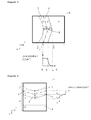
- FIGS 1-5 illustrate various TFETS according to embodiments of the present invention.
- Figures 6a -j illustrate by means of schematic top views and corresponding cross sections A-A a method of manufacturing of a vertical tunnelFET manufactured according to embodiments of the present invention.
- Figure 7 show a schematic cross section of a vertical heterostructure tunnel FET according to an embodiment of the present invention.
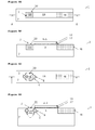
- Figures 8a -h illustrate by means of schematic top views and corresponding cross sections A-A a method of manufacturing a horizontal tunnel FET according to embodiments of the present invention.
- Figure 9 shows a schematic cross section of a horizontal tunnel FET manufactured according to another embodiment of the present invention.
- Figures 10a and 10b show respectively a top view and the corresponding schematic cross section A-A of a horizontal tunnel FET manufactured according to another embodiment of the present invention.
- Table 1 overview of reference numbers used 1 tunnel Field Effect Transistor 2 Source 3 Channel 4 Interface between source and channel 5 Source side interface layer 6 Channel side interface layer 7 first crystalline semiconductor material 8 Protrusion towards channel 9 Layer of second crystalline semiconductor material 10 Second crystalline semiconductor material 11 metal 12 Alloy of metal 11 and first crystalline semiconductor material 7 13 layer of alloy 12 14 layer of metal 11 15 source electrode 16 drain 17 gate dielectric 18 gate electrode 19 drain electrode 20 trench
- TFET tunnelling field effect transistor
- BBT Band-To-Band Tunnelling
- a TFET comprises typically a source-channel-drain configuration wherein the source and drain region are oppositely doped, i.e. for example the source region is p-type doped whereas the drain region is n-type doped or vice versa.
- the channel region is lower doped than source and drain regions or is undoped.
- TFET devices more specifically a TFET device comprising a horizontal source-channel-drain structure and a double gate electrode situated at least on the sidewalls of the channel region of the horizontal source-channel-drain structure
- TFET devices may be applied such as for example a tri-gate TFET, an all-round gate TFET, a nanowire TFET,....
- a tri-gate TFET comprises a horizontal source-channel-drain structure and a triple gate electrode situated on the sidewalls and on top of the channel and/or source region of the horizontal source-channel-drain structure.
- An all-around TFET comprises a horizontal or a vertical source-channel-drain structure and an all-around gate electrode situated around the channel and/or source region of the horizontal or vertical source-channel-drain structure.
- a nanowire TFET comprises a nanowire which forms at least the channel region and an all-around gate electrode structure around the channel and/or source region of the nanowire TFET. More specifically the fabrication method according to embodiments of the present invention relates to but is not limited to standard planar technology, double gate technology, finfet technology and nanotechnology, wherein the latter includes implementations with integrated nanowires.
- nTFET which means the semiconductor device comprises a p-type source, a channel contacted by a gate electrode, and a n-type drain
- a nTFET being often referred to as a p-i-n diode TFET
- TFET devices may be applied such as for example a pTFET, which means the semiconductor device comprises an n-type source, a channel contacted by a gate electrode, and a p-type drain.
- solubility level refers to that doping level above which clusters start to form if a dopant is added to a crystalline material. Such clusters may break the crystallinity of the material and is hence not wanted.
- FIGS 1-5 illustrate various embodiments of the present invention by means of schematic cross sections.
- Figure 1 shows a tunnel Field Effect Transistor 1 according to embodiments of the present invention, comprising an interface 4 between a source 2 and a channel 3.
- a layer 5 of a first crystalline semiconductor material 7 substantially uniformly doped with a metal 11 at a level below, up to and close to, e.g. not lower than 10% below, or not lower than 5% below, or not lower than 1% below the solubility level of the metal 11 in the first crystalline material 7.
- a layer 6 of this first crystalline semiconductor material 7 doped with this metal 11, the concentration thereof decreasing towards the channel.
- the source side interface layer 5 is furthermore substantially uniformly doped with another dopant such that a total concentration level of metal dopants and the another dopant is obtained, indicated hereinafter N 5 , and the channel side interface layer 6 is then doped with this another dopant, the total dopant concentration level in this channel side interface layer 6 decreasing from this concentration level N 5 towards the channel 3.
- Adding the another dopant may be done in order to increase the on-current of the TFET.
- Al has a solubility limit of 1e19 at/cm 3 in Si. If it is desired to obtain a higher doping, for example, but not limited thereto, up to 1e20 at/cm 3 , another dopant may be added.
- the source side interface layer 5 has a thickness t 5 between 5 nm and 100 nm and a (substantially constant) concentration level N 5 of at least 1e19/cm 3 .
- the channel side interface layer 6 has typically a thickness t 6 between 5 nm to 100 nm and a concentration gradient of the dopants between 10 nm/dec to 1 nm/dec.
- the plane of the interface 4 may be a ⁇ 111 ⁇ plane.
- the interface 4 is substantially planar, in which case the ⁇ 111 ⁇ plane is lying in the y-z plane parallel to the substrate.
- Figure 1 illustrates a vertical type Field Effect Transistor.
- the source 2 can protrude towards and into the channel 3 thereby forming a pyramidal-like structure 8 into the channel 3.
- the sidewalls of this protrusion 8 form the interface 4 and are lying in a ⁇ 111 ⁇ plane.
- Figure 2 shows a vertical type of a Field Effect Transistor 1 wherein the source 2 protrudes into the channel 3 along the x direction.
- Figure 3 shows a horizontal type of such a Field Effect Transistor 1 wherein the source 2 protrudes into the channel 3 along the y direction.
- the source 2 and channel 3 are formed from the same crystalline semiconductor material 7.
- a TFET is known as homostructure TFET.
- the channel 3 can further comprise a layer 9 of a second crystalline semiconductor material 10 adjacent to the channel side of the first crystalline semiconductor material 7 and possibly adjacent to the channel side of the interface layer 6 resulting in a heterojunction between the first crystalline semiconductor material 7 and the second crystalline semiconductor material 10.
- a TFET is known as heterostructure TFET.
- the source 2 of the tunnel Field Effect Transistors 1 illustrated by figures 1 to 4 can further comprise a layer 13 of an alloy 12 of the first crystalline semiconductor material 7 and the metal 11, the alloy layer 12 contacting the source side interface layer 5.
- the first crystalline semiconductor material 7 may be Si x Ge 1-x with 0 ⁇ x ⁇ 1.
- the metal 11 may be Aluminium. If this Aluminium 11 is doped with another dopant, preferably this another dopant is Boron, and this another dopant will become a dopant of the source side interface layer 5 and the channel side interface layer 6.
- Figures 6a to 6j show schematic representations of the top view and corresponding schematic representations of the cross-section AA of a vertical TFET structure comprising a pyramidal shaped source region 3 according to embodiments of the present invention, during different manufacturing steps.
- this substrate may be a crystalline semiconductor substrate such as a silicon substrate or a semiconductor-on-insulator (SOI) substrate but any other suitable substrate supporting a crystalline semiconductor layer 7 can be used as well, such as, for example, glass, ceramics, etc.
- a crystalline semiconductor substrate such as a silicon substrate or a semiconductor-on-insulator (SOI) substrate
- SOI semiconductor-on-insulator
- a drain 16 and channel 3 are provided on the semiconductor substrate as shown in figures 6a and 6b .
- the channel 3 is in contact with the drain 16.
- the drain 16 and the channel 3 may be formed by epitaxial growth of semiconductor material 10,7 of the drain 16 and channel 3 on the semiconductor substrate or layer.
- nanostructures may be etched from an undoped substrate after which the bottom region of the thus formed nanostructure is implanted thereby forming the doped drain 16.
- the drain 16 may be made of a semiconductor material which is highly n-doped in case of an n-type TFET, or alternatively in case of a p-type TFET the drain 16 is highly p-doped.
- the doping level of the drain 16 is typically in the range of 1e18/cm 3 to 1e21/cm 3 , for example in the range of 1e19/cm 3 to 5e20/cm 3 .
- the channel 3 can be made of a semiconductor material 7, 10 which is the same or different from the semiconductor material of the drain 16, thereby forming respectively a homojunction or heterojunction between the channel 3 and the drain 16.
- the channel 3 may for example be undoped or at least lower doped than the drain 16, e.g. having a dopant concentration level which is at least a factor 10 lower than the dopant concentration level of the drain 16.
- the doping level of the channel 3 may be in the range of undoped up to 1e17/cm 3 doping, for example in the range of undoped up to 1e15/cm 3 doping.
- a gate comprising agate dielectric 17 and gate electrode 18,is provided as shown in figures 6a and 6b .
- the gate more specifically the gate dielectric 17 of the gate 10, is at least in contact with the channel 3 of the TFET device 1.
- the gate is an all-around gate, covering the circumference of the channel 3.
- the device could for instance be a double-gate device, with the gate only covering two sides of the circumference of the channel, or a tri-gate device, with the gate covering three sides of the circumference of the channel.
- the crystalline semiconductor substrate has a [100] orientation. Then a shaped source 2 is provided in contact with the channel 3 as such forming a tip-shaped source-channel interface 4 between the source 2 and the channel 3. Otherwise said, the interface 4 between the source 2 and the channel 3 is not a plane but has a tip-like shape 8, as illustrated in the cross-sections of any of figures 2 to 5 .
- tip-like shape is meant that the source 2 has a pyramidal shape with the tip 8 extending into the channel region or that the source 2 has a knife-edged shape with the knife edge 8 extending into the channel region or that the source 2 has a conical shape with an apex 8 extending into the channel region or that the source 2 has a conical shape with a knife-edge apex 8 extending into the channel region.
- the source 2 is formed by a plurality of layers.
- the first layer is a layer 5 of the first crystalline semiconductor material 7 of which also the channel is made, substantially uniformly doped with a metal 11. This first layer 5 may furthermore be doped with another dopant as set out above.
- the alloy formed 12 may be pyramidal shaped or knife-edge shaped resulting in a shaped source 2.
- Figures 6e and 6f illustrate a pyramidal shaped source region 3 having 1 apex. The contact area between the metal layer 14 and the source region 3 was square.
- Figures 6g and 6h illustrate a knife-shaped source region having 2 apexes. Here the contact area between the metal layer 11 and the source region 3 was rectangular.
- the channel 3, after the step of providing a channel 3 in contact with the drain 16, has a cuboid shape with a rectangular top surface which is substantially parallel to the semiconductor substrate surface plane.
- the sidewalls of the cuboid channel are substantially orthogonally oriented with respect to the semiconductor substrate surface plane.
- a channel having a cuboid shape with a rectangular top surface is also referred to as a rectangular cuboid channel 3.
- the channel 3, after the step of providing a channel 3 in contact with the drain 16, has a cuboid shape with a square top surface which is substantially parallel to the semiconductor substrate surface plane.
- the sidewalls of the cuboid channel are substantially orthogonally oriented with respect to the semiconductor substrate surface plane.
- a channel 3 having a cuboid shape with a square top surface is also referred to as a square cuboid channel 3.
- the channel 3, after the step of providing a channel 3 in contact with the drain 16, has a cylindrical shape with an elliptical top surface which is substantially parallel to the semiconductor substrate surface plane.
- the curved sidewall of the cylindrical channel is substantially orthogonally oriented with respect to the semiconductor substrate surface plane.
- a channel 3 having a cylindrical shape with an elliptical top surface is also referred to as an elliptic cylindrical channel.
- the channel 3 after the step of providing a channel 3 in contact with the drain 16, has a cylindrical shape with a circular top surface which is substantially parallel to the semiconductor substrate surface plane.
- the curved sidewall of the cylindrical channel 3 is substantially orthogonally oriented with respect to the semiconductor substrate surface plane.
- a channel 3 having a cylindrical shape with a circular top surface is also referred to as a circular cylindrical channel.
- a layer of metal 11 is provided on top of the first crystalline semiconductor material 7 in which the channel 3 is formed and the source 2 is to be formed.
- dissolution of Al in Si is much easier in the ⁇ 111 ⁇ planes, and hence a pyramidal shape consisting of 4 ⁇ 111 ⁇ planes is obtained.
- the eutectic system is responsible for the Al-doped Si crystalline formation.
- the dissolution rate of Al in Si is strongly dependent on the crystal planes (lowest dissolution rate is for ⁇ 111 ⁇ -plane due to the highest packing density), anisotropic behaviour is achieved and shapes similar to anisotropic wet etching are created.
- the source 2 will be knife-edge pyramidal shaped.
- the source 2 will be pyramidal shaped.
- the source 2 will be knife-edge shaped, wherein the dimensions of the ellipse will determine the length and width of the shape.
- the source 2 In the case of a cylindrical channel 3, the source 2 will be pyramidal shaped.
- An advantage of the technique in accordance with embodiments of the present invention is that in the undoped region surrounding the part of the source protruding into the channel, no defects have been generated (e.g. typically defects are generated by implantation damage or by dislocations, which are not present here). Defects typically cause worse subthreshold swing, as they allow for current to flow when band-to-band tunnelling is not yet possible. Hence embodiments of the present invention provide a good, e.g. better than in prior art, subthreshold swing.
- Figures 6a and 6b show a tunnel FET 1 comprising a cuboid channel 3 in contact with a drain 16 on a drain electrode 19.
- a gate stack is provided comprising a gate dielectric 17 and a gate electrode 18.
- the step of providing a source 2 in contact with the channel 3 as such forming a tip-shaped source-channel interface 4 with the channel 3 comprises different substeps.
- a layer 14 of a metal 11 is provided on top of the first crystalline semiconductor material 7 in which the source 2 and the channel 3 are to be formed.
- the metal layer 14 may for example consist of an Aluminium layer.
- the metal layer 14 is provided on the surface of the crystalline semiconductor material 7 of the channel 3 which is exposed after the step of providing the channel 3.
- Providing the metal 11 may comprise depositing a metal layer 14 over the whole structure, i.e. the channel 3 and gate stack 17-18, and patterning the metal layer 14 such that the metal 11 remains only present on top of the channel 3 and in contact with the first crystalline semiconductor material 7.
- the metal layer 14 may be deposited using physical vapour deposition (PVD) or sputtering, chemical vapour deposition, screen printing,....
- the thickness of the as-deposited metal layer 14 is in the range of 10 nm up to 1 micrometer.
- a doped metal layer 14 may be provided in contact with the channel 3.
- the metal 11 of layer 14 may be doped with a p-type dopant, called a further dopant hereinabove, such as for example Boron.
- the metal 11 may be doped with an n-type dopant, such as for example As.
- a doped Aluminium layer may be provided.
- the Aluminium layer may be doped with a p-type dopant, such as for example Boron, resulting in an Al-B layer.
- the Aluminium layer may be doped with an n-type dopant, such as for example As, resulting in an Al-As layer.
- the dopant of the metal 11 is selected in view of the dopant level and dopant type of the interface layers 5, 6 that are to be formed as will be discussed further on.
- the metal 11 must consist of a material which has a self-formation of a shape, e.g. tip or wedge-shape, in the host lattice, i.e. first crystalline semiconductor material 7, upon alloying, i.e. heat treatment and cooling down, and which may be, but not necessarily is a dopant of the host lattice.
- the metal layer is selected to form a semiconductor alloy in an anisotropic way.
- p-type dopants B, Al, Ga, In, Tl, Pd, Na, Be, Zn, Au, Co, V, Ni, MO, Hg, Sr, Ge, Cu, K, Sn, W, Pb, O, Fe.
- n-type dopants Li, Sb, P, As, Bi, Te, Ti, C, Mg, Se, Cr, Ta, Cs, Ba, S, Mn, Ag, Cd, Pt.
- p-type dopants B, Al, Tl, Ga, In, Be, Zn, Cr, Cd, Hg, Co, Ni, Mn, Fe, Pt.
- n-type dopants Li, Sb, P, As, S, Se, Te, Cu, Au, Ag.
- a shaped metal-semiconductor alloy 12 is formed by alloying the metal material 11 of the layer 14 with the semiconductor material 7 of the channel 3, as shown in figures 6e and 6f for a tip-shaped alloy 12 or 6g and 6h for a wedge-shaped alloy 12.
- the tip-shaped metal-semiconductor alloy 12 comprises metal material 11 from the as-deposited metal layer 14 and first crystalline semiconductor material 7 from the semiconductor channel 3 and also comprises a tip-shaped highly doped semiconductor layer 5 at the tip-shaped source-channel interface 4, the tip-shaped metal-semiconductor alloy 12 protruding 8 towards and penetrating into the channel 3 thereby forming the tip-shaped source-channel interface 4.
- Forming the metal-semiconductor alloy 12 comprises performing a heat treatment and thereafter cooling down.
- the maximum temperature at which the heat treatment is performed may depend on the first crystalline semiconductor material 7.
- silicon 7 the heat treatment is at least at 650°C, typically at 800°C, but can be higher than 800°C.
- Germanium 7 the heat treatment is at least at 450°C but can be higher.
- a rapid thermal annealing step may be used for example.
- an Al-Si 12, 7 alloy may be formed by first heating the structure comprising the as-deposited Aluminium layer 14 on top of the Si channel 3. During this heating step the first crystalline semiconductor material 7, i.e. the silicon 7 from the channel 3 will dissolve into the Aluminium 11 of the layer 14.
- Al-Si 11,7 dissolved structure is then cooled down, several layers are formed, more specifically an Al-Si matrix layer (replacing the as-deposited Aluminium layer 14) in contact with an Al-Si alloy 12 (which penetrates into the original silicon channel 3).
- This Al-Si alloy 12 contacts a thin layer 5 being a highly metal 11 doped crystalline semiconductor layer 5 at the interface 4 and a lower metal doped crystalline semiconductor layer 6 at the opposite side of the interface 4.
- the doped semiconductor layers 5 and 6 are formed first. The remaining liquid solidifies at the eutectic temperature leading to the Al-Si alloy 12. The rest of the material forms a matrix layer of Al-Si particles.
- the Al concentration near the source-channel interface 4 is reduced leaving a highly doped semiconductor source side interface layer 5 and a lower doped semiconductor channel side interface layer 6.
- the resulting metal-semiconductor alloy 12 and doped semiconductor layers 5,6 formed at the surface of this metal-semiconductor alloy 12 has a pyramidal shape with the point of the pyramid protruding towards the channel 3.
- the pyramidal shape is obtained due to the different dissolution speeds which occur at different crystallographic planes, for example at the ⁇ 100 ⁇ and ⁇ 111 ⁇ planes.
- a tip-shaped source 2 is formed, the tip-shaped source 2 comprising a tip-shaped highly doped semiconductor interface layer 5 at the channel-source interface 4 and a tip-shaped metal semiconductor alloy 12 in contact with the tip-shaped highly doped semiconductor interface layer 5.
- the tip-shaped source 2 is protruding in the as-formed channel 3, such that the apex or end point of the tip-shaped source 2 is located in the as-formed channel 3.
- the resulting channel 3 becomes thus smaller than the as-formed channel 3 due to the penetration of the metal-semiconductor alloy 12 into the channel 3 and formation of the highly doped semiconductor interface layer 5 from the tip-shaped source region 3.
- a source electrode 15 can be formed on the alloy 12.
- FIGS 6i and 6j show a schematic representation of the resulting structure after complete removal of the semiconductor-metal alloy 12 and formation of the source electrode 15.
- the tip-shaped source 2 then consists of only the highly doped semiconductor layer 5.
- part of the metal-semiconductor alloy 12 may still be present.
- By completely removing the metal-semiconductor alloy 12 a tip-shaped opening is formed.
- the tip-shaped opening may be filled completely or partially with a source contact material as shown in figures 6i and 6j . Otherwise, on top of the tip-shaped source 2, i.e. highly doped semiconductor layer 5 or semiconductor-metal alloy 12 if not completely removed, a source electrode 15 may be formed.
- the source 2 comprising the highly doped semiconductor layer 5 a very sharp transition in doping level is formed from the highly doped source 2 toward the lower doped channel 3. Depending on the crystal orientation of the semiconductor substrate, this source 2 also comprises a tip 8 extending towards the channel 3. Otherwise said, an abrupt interface 4 may be formed between the source 2 and the channel 3 of the TFET structure 1.
- Figure 7 illustrates a vertical tunnel FET where a highly doped source side interface layer 5 is formed at the interface 4 between the source 2 and the channel 3.
- the source 2 is flat without an apex 8 pointing towards the channel 3.
- a silicon substrate having a [100] crystal orientation was chosen, here a silicon substrate having a ⁇ 111 ⁇ crystal orientation is chosen for illustrating this embodiment having a planar interface 4.
- a metal layer such as an Aluminium layer 14 is deposited on the channel 3
- a metal-semiconductor alloy 12 is formed when heating up and cooling down the substrate.
- the Al-Si alloy 12 will grow uniformly into the first crystalline semiconductor substrate 7 resulting in a planar interface 4.
- the alloying metal layer 14 can be doped; either during providing this metal 11 or afterwards using ion implantation.
- the semiconductor alloy 12 is completely removed and an additional source electrode 15 is contacting this highly doped source side interface layer 5.
- the semiconductor alloy 12 was formed by the interaction between the metal 11 provided to crystalline semiconductor material 7 wherein the channel 3 is to be formed.
- FIGS 8a -h showing schematic top views and corresponding cross sections A-A, describing methods for manufacturing a horizontal TFET structure with a shaped source-channel interface 4.
- Figures 8a-8h show different steps of the top view and corresponding cross-sectional view A-A of a horizontal TFET device manufactured according to embodiments of the present invention.
- Figure 8a and figure 8b schematically show a semiconductor 7 substrate wherein a drain 16 and gate stack 17, 18 are formed. The location of the source 2 and the channel 3 is indicated.
- Figure 8c and figure 8d schematically show providing an opening 20 in semiconductor 7 substrate at the location of the source 2.
- This opening 20 is thereafter filled with the alloying metal 11 as shown in figures 8e and 8f .
- the opening in the example illustrated, has a rectangular cross-section in a direction parallel to the plane of the substrate 7.
- a shaped source 2 is formed in contact with the channel 3 as such forming a shaped source-channel interface 4.
- the shaped source 2 and the interface layers 5, 6 are formed as described above in detail by forming a metal-semiconductor alloy 12.
- the interface layers 5, 6 at the border between the semiconductor metal alloy 12 and the semiconductor material 7, from which the alloy 12 is formed, are not shown in figures 8g and 8h .
- Figure 9 schematically shows a schematic cross section of an alternative embodiment wherein the semiconductor substrate comprises an SOI substrate.
- the semiconductor layer of the semiconductor-on-insulator substrate is used as the first crystalline semiconductor material 7.
- the underlying insulator layer is illustrated in figure 9 and indicated BOX.
- the yet underlying substrate layer is not illustrated in the drawings.
- the trench 20 in the semiconductor substrate at the location of the source 2 is in this case formed, and thereafter filled with the metal 11, down to the semiconductor-oxide interface of the SOI substrate, i.e. down to the so-called buried oxide layer BOX of the SOI substrate. In this embodiment no tip is formed pointing towards the underlying substrate as the buried oxide prevents this.
- the shape of the source 2 depends on the shape of the contact area between the layer 14 of the alloying metal 11 and the source 2. For a horizontal tunnel FET, this contact area is determined by the dimensions of the opening 20 formed in the semiconductor 7 substrate. When a square opening is formed, the shaped source 2 will resemble a pyramidal shape as illustrated in figures 8a to 8h . When a more rectangular opening is formed, the shaped source 2 will more resemble a wedge shape.
- the shape of the source 2 depends on shape of the contact area between the layer 14 of the alloying metal 11 and the source 2. For a horizontal tunnel FET, this contact area is determined by the dimensions of the vertical side planes of the opening 20 formed in the semiconductor 7 substrate. When a square vertical side plane of the opening is formed, the shaped source 2 will resemble a pyramidal shape as illustrated in figures 8a to 8h . When a more rectangular vertical side plane of the opening is formed, the shaped source 2 will more resemble a wedge shape. The latter embodiment is illustrated in figures 10a and 10b. Figure 10b show the cross section A-A of figure 10a . Only the interface 4 is indicated in these figures.
Landscapes
- Thin Film Transistor (AREA)
- Insulated Gate Type Field-Effect Transistor (AREA)
- Bipolar Transistors (AREA)
Priority Applications (1)
| Application Number | Priority Date | Filing Date | Title |
|---|---|---|---|
| EP12198391.0A EP2608263A3 (de) | 2011-12-21 | 2012-12-20 | Tunnel-Feldeffekt-Transistor und Verfahren zur Herstellung davon |
Applications Claiming Priority (2)
| Application Number | Priority Date | Filing Date | Title |
|---|---|---|---|
| EP11194802 | 2011-12-21 | ||
| EP12198391.0A EP2608263A3 (de) | 2011-12-21 | 2012-12-20 | Tunnel-Feldeffekt-Transistor und Verfahren zur Herstellung davon |
Publications (2)
| Publication Number | Publication Date |
|---|---|
| EP2608263A2 true EP2608263A2 (de) | 2013-06-26 |
| EP2608263A3 EP2608263A3 (de) | 2014-04-23 |
Family
ID=47435801
Family Applications (1)
| Application Number | Title | Priority Date | Filing Date |
|---|---|---|---|
| EP12198391.0A Withdrawn EP2608263A3 (de) | 2011-12-21 | 2012-12-20 | Tunnel-Feldeffekt-Transistor und Verfahren zur Herstellung davon |
Country Status (3)
| Country | Link |
|---|---|
| US (1) | US8872230B2 (de) |
| EP (1) | EP2608263A3 (de) |
| JP (1) | JP6146997B2 (de) |
Families Citing this family (4)
| Publication number | Priority date | Publication date | Assignee | Title |
|---|---|---|---|---|
| CN102664192B (zh) * | 2012-05-08 | 2015-03-11 | 北京大学 | 一种自适应复合机制隧穿场效应晶体管及其制备方法 |
| KR102157825B1 (ko) | 2014-01-16 | 2020-09-18 | 삼성전자주식회사 | 터널링 전계 효과 트랜지스터 |
| US10424581B2 (en) * | 2016-04-18 | 2019-09-24 | Samsung Electronics Co., Ltd. | Sub 59 MV/decade SI CMOS compatible tunnel FET as footer transistor for power gating |
| US11164939B2 (en) * | 2018-06-27 | 2021-11-02 | Taiwan Semiconductor Manufacturing Co., Ltd. | Tunnel field-effect transistor and method for forming the same |
Family Cites Families (19)
| Publication number | Priority date | Publication date | Assignee | Title |
|---|---|---|---|---|
| US5808340A (en) | 1996-09-18 | 1998-09-15 | Advanced Micro Devices, Inc. | Short channel self aligned VMOS field effect transistor |
| JP4213776B2 (ja) * | 1997-11-28 | 2009-01-21 | 光照 木村 | Mosゲートショットキートンネルトランジスタおよびこれを用いた集積回路 |
| US6232633B1 (en) | 1998-06-08 | 2001-05-15 | International Business Machines Corporation | NVRAM cell using sharp tip for tunnel erase |
| US7244996B2 (en) * | 2000-04-06 | 2007-07-17 | Oki Electric Industry Co., Ltd. | Structure of a field effect transistor having metallic silicide and manufacturing method thereof |
| US6833556B2 (en) * | 2002-08-12 | 2004-12-21 | Acorn Technologies, Inc. | Insulated gate field effect transistor having passivated schottky barriers to the channel |
| JP4488870B2 (ja) * | 2004-11-19 | 2010-06-23 | 株式会社東芝 | 半導体素子と半導体装置 |
| US7208379B2 (en) | 2004-11-29 | 2007-04-24 | Texas Instruments Incorporated | Pitch multiplication process |
| US20060202266A1 (en) * | 2005-03-14 | 2006-09-14 | Marko Radosavljevic | Field effect transistor with metal source/drain regions |
| JP2006344804A (ja) * | 2005-06-09 | 2006-12-21 | Seiko Epson Corp | 半導体装置および半導体装置の製造方法 |
| US7494858B2 (en) * | 2005-06-30 | 2009-02-24 | Intel Corporation | Transistor with improved tip profile and method of manufacture thereof |
| EP1900681B1 (de) * | 2006-09-15 | 2017-03-15 | Imec | Tunnelfeldeffekttransistoren auf der Basis von Siliziumnanodrähte |
| US8148718B2 (en) | 2007-05-31 | 2012-04-03 | The Regents Of The University Of California | Low voltage transistors |
| US7936009B2 (en) | 2008-07-09 | 2011-05-03 | Fairchild Semiconductor Corporation | Shielded gate trench FET with an inter-electrode dielectric having a low-k dielectric therein |
| US7834345B2 (en) * | 2008-09-05 | 2010-11-16 | Taiwan Semiconductor Manufacturing Company, Ltd. | Tunnel field-effect transistors with superlattice channels |
| US20110241116A1 (en) * | 2010-04-06 | 2011-10-06 | International Business Machines Corporation | FET with FUSI Gate and Reduced Source/Drain Contact Resistance |
| EP2378557B1 (de) * | 2010-04-19 | 2015-12-23 | Imec | Verfahren zur Herstellung eines vertikalen TFET |
| CN101901837A (zh) * | 2010-06-24 | 2010-12-01 | 复旦大学 | 一种栅控pn场效应晶体管及其控制方法 |
| US8354694B2 (en) * | 2010-08-13 | 2013-01-15 | International Business Machines Corporation | CMOS transistors with stressed high mobility channels |
| CN102593000B (zh) * | 2011-01-13 | 2015-01-14 | 中国科学院微电子研究所 | 半导体器件及其制造方法 |
-
2012
- 2012-11-16 US US13/679,052 patent/US8872230B2/en active Active
- 2012-12-20 EP EP12198391.0A patent/EP2608263A3/de not_active Withdrawn
- 2012-12-21 JP JP2012278855A patent/JP6146997B2/ja active Active
Non-Patent Citations (2)
| Title |
|---|
| P. F. WANG; K. HILSENBECK; TH. NIRSCHL ET AL., SOLID-STATE ELECTRONICS, vol. 48, 2004, pages 2281 |
| YUE YANG ET AL.: "Drive current enhancement with invasive source in double gate tunneling field-effect transistors", EXTENDED ABSTRACTS OF THE 2010 INTERNATIONAL CONFERENCE ON SOLID STATE DEVICES AND MATERIALS (SSDM, pages 798 - 799 |
Also Published As
| Publication number | Publication date |
|---|---|
| JP6146997B2 (ja) | 2017-06-14 |
| US8872230B2 (en) | 2014-10-28 |
| US20130161696A1 (en) | 2013-06-27 |
| JP2013153151A (ja) | 2013-08-08 |
| EP2608263A3 (de) | 2014-04-23 |
Similar Documents
| Publication | Publication Date | Title |
|---|---|---|
| US8431924B2 (en) | Control of tunneling junction in a hetero tunnel field effect transistor | |
| US8404545B2 (en) | Tunnel field-effect transistor with gated tunnel barrier | |
| US8629428B2 (en) | Line-tunneling tunnel field-effect transistor (TFET) and manufacturing method | |
| US9318583B2 (en) | Tunnel field effect transistor and method for making thereof | |
| EP2920815B1 (de) | Tunnelfeldeffekttransistoren (tfets) für cmos-architekturen und verfahren zur herstellung von tfets vom n-typ und p-typ | |
| TWI534864B (zh) | 具凹入合併鰭及襯底的絕緣層上半導體鰭式場效電晶體用以加強應力偶合 | |
| US8653504B2 (en) | Complementary tunneling field effect transistor and method for forming the same | |
| EP2870632B1 (de) | Radiale nanodraht esaki-dioden-vorrichtungen und dazugehörige verfahren | |
| EP1900681B1 (de) | Tunnelfeldeffekttransistoren auf der Basis von Siliziumnanodrähte | |
| CN102054870A (zh) | 一种半导体结构及其形成方法 | |
| CN102142461B (zh) | 栅控肖特基结隧穿场效应晶体管及其形成方法 | |
| WO2012152762A1 (en) | Tunnel field effect transistor device | |
| US10896974B2 (en) | Method of fabricating semiconductor device | |
| CN113178489B (zh) | 一种z2-fet器件及其制备方法、一种半导体器件 | |
| US8637851B2 (en) | Graphene device having physical gap | |
| US8872230B2 (en) | Tunnel field-effect transistor and methods for manufacturing thereof | |
| CN113178490A (zh) | 一种隧穿场效应晶体管及其制备方法 | |
| KR102273935B1 (ko) | 음성 트랜스 컨덕턴스 기반의 터널링 트랜지스터 | |
| WO2016029711A1 (zh) | 一种隧穿场效应晶体管及其制作方法 | |
| CN203521424U (zh) | 半栅极控制源极肖特基势垒型隧穿场效应晶体管 | |
| KR101402697B1 (ko) | 독립적 및 대칭적인 이중 게이트 구조를 이용한 전자-정공 이중층 터널 전계 효과 트랜지스터 및 그 제조 방법 | |
| US8853674B2 (en) | Tunneling field effect transistor structure and method for forming the same | |
| ZHAO et al. | nanowire MOSFET |
Legal Events
| Date | Code | Title | Description |
|---|---|---|---|
| AK | Designated contracting states |
Kind code of ref document: A2 Designated state(s): AL AT BE BG CH CY CZ DE DK EE ES FI FR GB GR HR HU IE IS IT LI LT LU LV MC MK MT NL NO PL PT RO RS SE SI SK SM TR |
|
| AX | Request for extension of the european patent |
Extension state: BA ME |
|
| PUAI | Public reference made under article 153(3) epc to a published international application that has entered the european phase |
Free format text: ORIGINAL CODE: 0009012 |
|
| PUAL | Search report despatched |
Free format text: ORIGINAL CODE: 0009013 |
|
| AK | Designated contracting states |
Kind code of ref document: A3 Designated state(s): AL AT BE BG CH CY CZ DE DK EE ES FI FR GB GR HR HU IE IS IT LI LT LU LV MC MK MT NL NO PL PT RO RS SE SI SK SM TR |
|
| AX | Request for extension of the european patent |
Extension state: BA ME |
|
| RIC1 | Information provided on ipc code assigned before grant |
Ipc: H01L 29/10 20060101AFI20140319BHEP Ipc: H01L 29/739 20060101ALI20140319BHEP Ipc: H01L 29/36 20060101ALI20140319BHEP Ipc: H01L 29/66 20060101ALI20140319BHEP |
|
| 17P | Request for examination filed |
Effective date: 20141020 |
|
| RBV | Designated contracting states (corrected) |
Designated state(s): AL AT BE BG CH CY CZ DE DK EE ES FI FR GB GR HR HU IE IS IT LI LT LU LV MC MK MT NL NO PL PT RO RS SE SI SK SM TR |
|
| RAP1 | Party data changed (applicant data changed or rights of an application transferred) |
Owner name: IMEC VZW |
|
| STAA | Information on the status of an ep patent application or granted ep patent |
Free format text: STATUS: EXAMINATION IS IN PROGRESS |
|
| 17Q | First examination report despatched |
Effective date: 20190327 |
|
| GRAP | Despatch of communication of intention to grant a patent |
Free format text: ORIGINAL CODE: EPIDOSNIGR1 |
|
| STAA | Information on the status of an ep patent application or granted ep patent |
Free format text: STATUS: GRANT OF PATENT IS INTENDED |
|
| RIC1 | Information provided on ipc code assigned before grant |
Ipc: H01L 29/10 20060101ALI20200925BHEP Ipc: H01L 29/04 20060101ALI20200925BHEP Ipc: H01L 29/08 20060101ALI20200925BHEP Ipc: H01L 29/06 20060101ALI20200925BHEP Ipc: H01L 21/33 20060101ALI20200925BHEP Ipc: H01L 29/739 20060101AFI20200925BHEP Ipc: H01L 29/36 20060101ALI20200925BHEP |
|
| INTG | Intention to grant announced |
Effective date: 20201020 |
|
| STAA | Information on the status of an ep patent application or granted ep patent |
Free format text: STATUS: THE APPLICATION IS DEEMED TO BE WITHDRAWN |
|
| 18D | Application deemed to be withdrawn |
Effective date: 20210302 |