EP2593980B1 - Verfahren zur herstellung einer oled-vorrichtung - Google Patents
Verfahren zur herstellung einer oled-vorrichtung Download PDFInfo
- Publication number
- EP2593980B1 EP2593980B1 EP11744090.9A EP11744090A EP2593980B1 EP 2593980 B1 EP2593980 B1 EP 2593980B1 EP 11744090 A EP11744090 A EP 11744090A EP 2593980 B1 EP2593980 B1 EP 2593980B1
- Authority
- EP
- European Patent Office
- Prior art keywords
- layer
- conductive
- transfer
- onto
- oled device
- Prior art date
- Legal status (The legal status is an assumption and is not a legal conclusion. Google has not performed a legal analysis and makes no representation as to the accuracy of the status listed.)
- Not-in-force
Links
- 238000004519 manufacturing process Methods 0.000 title claims description 9
- 239000010410 layer Substances 0.000 claims description 59
- 239000011241 protective layer Substances 0.000 claims description 44
- 238000000034 method Methods 0.000 claims description 34
- 239000000565 sealant Substances 0.000 claims description 20
- 239000012044 organic layer Substances 0.000 claims description 17
- 239000000758 substrate Substances 0.000 claims description 14
- 238000000151 deposition Methods 0.000 claims description 13
- 239000011888 foil Substances 0.000 claims description 12
- 230000009931 harmful effect Effects 0.000 claims description 5
- 239000004033 plastic Substances 0.000 claims description 2
- 229920003023 plastic Polymers 0.000 claims description 2
- 229910052751 metal Inorganic materials 0.000 description 50
- 239000002184 metal Substances 0.000 description 50
- 239000000853 adhesive Substances 0.000 description 20
- 230000001070 adhesive effect Effects 0.000 description 20
- 239000000463 material Substances 0.000 description 17
- 230000007797 corrosion Effects 0.000 description 11
- 238000005260 corrosion Methods 0.000 description 11
- BQCADISMDOOEFD-UHFFFAOYSA-N Silver Chemical compound [Ag] BQCADISMDOOEFD-UHFFFAOYSA-N 0.000 description 7
- 239000000976 ink Substances 0.000 description 7
- 150000002739 metals Chemical class 0.000 description 7
- 229910052709 silver Inorganic materials 0.000 description 7
- 239000004332 silver Substances 0.000 description 7
- ZOKXTWBITQBERF-UHFFFAOYSA-N Molybdenum Chemical compound [Mo] ZOKXTWBITQBERF-UHFFFAOYSA-N 0.000 description 6
- 229910052750 molybdenum Inorganic materials 0.000 description 6
- 239000011733 molybdenum Substances 0.000 description 6
- 239000011521 glass Substances 0.000 description 5
- PCHJSUWPFVWCPO-UHFFFAOYSA-N gold Chemical compound [Au] PCHJSUWPFVWCPO-UHFFFAOYSA-N 0.000 description 5
- 229910052737 gold Inorganic materials 0.000 description 5
- 239000010931 gold Substances 0.000 description 5
- 238000007789 sealing Methods 0.000 description 5
- VYZAMTAEIAYCRO-UHFFFAOYSA-N Chromium Chemical compound [Cr] VYZAMTAEIAYCRO-UHFFFAOYSA-N 0.000 description 4
- 229910052804 chromium Inorganic materials 0.000 description 4
- 239000011651 chromium Substances 0.000 description 4
- 239000011248 coating agent Substances 0.000 description 4
- 238000000576 coating method Methods 0.000 description 4
- 239000004020 conductor Substances 0.000 description 4
- 238000013459 approach Methods 0.000 description 3
- 238000010586 diagram Methods 0.000 description 3
- 238000005538 encapsulation Methods 0.000 description 3
- 239000004698 Polyethylene Substances 0.000 description 2
- QVGXLLKOCUKJST-UHFFFAOYSA-N atomic oxygen Chemical compound [O] QVGXLLKOCUKJST-UHFFFAOYSA-N 0.000 description 2
- 230000000052 comparative effect Effects 0.000 description 2
- 230000001419 dependent effect Effects 0.000 description 2
- 230000000694 effects Effects 0.000 description 2
- 230000002349 favourable effect Effects 0.000 description 2
- 239000001301 oxygen Substances 0.000 description 2
- 229910052760 oxygen Inorganic materials 0.000 description 2
- 238000000206 photolithography Methods 0.000 description 2
- -1 polyethylene Polymers 0.000 description 2
- 229920000573 polyethylene Polymers 0.000 description 2
- 208000032368 Device malfunction Diseases 0.000 description 1
- 239000013590 bulk material Substances 0.000 description 1
- 230000008021 deposition Effects 0.000 description 1
- 238000009826 distribution Methods 0.000 description 1
- 239000007789 gas Substances 0.000 description 1
- 238000002955 isolation Methods 0.000 description 1
- 239000000155 melt Substances 0.000 description 1
- 239000000203 mixture Substances 0.000 description 1
- 230000009972 noncorrosive effect Effects 0.000 description 1
- 239000011253 protective coating Substances 0.000 description 1
- 230000001681 protective effect Effects 0.000 description 1
- 239000002356 single layer Substances 0.000 description 1
- 230000000007 visual effect Effects 0.000 description 1
Images

Classifications
-
- H—ELECTRICITY
- H05—ELECTRIC TECHNIQUES NOT OTHERWISE PROVIDED FOR
- H05B—ELECTRIC HEATING; ELECTRIC LIGHT SOURCES NOT OTHERWISE PROVIDED FOR; CIRCUIT ARRANGEMENTS FOR ELECTRIC LIGHT SOURCES, IN GENERAL
- H05B33/00—Electroluminescent light sources
- H05B33/02—Details
- H05B33/04—Sealing arrangements, e.g. against humidity
-
- H—ELECTRICITY
- H10—SEMICONDUCTOR DEVICES; ELECTRIC SOLID-STATE DEVICES NOT OTHERWISE PROVIDED FOR
- H10K—ORGANIC ELECTRIC SOLID-STATE DEVICES
- H10K50/00—Organic light-emitting devices
- H10K50/80—Constructional details
- H10K50/805—Electrodes
-
- H—ELECTRICITY
- H10—SEMICONDUCTOR DEVICES; ELECTRIC SOLID-STATE DEVICES NOT OTHERWISE PROVIDED FOR
- H10K—ORGANIC ELECTRIC SOLID-STATE DEVICES
- H10K50/00—Organic light-emitting devices
- H10K50/80—Constructional details
- H10K50/84—Passivation; Containers; Encapsulations
- H10K50/842—Containers
- H10K50/8426—Peripheral sealing arrangements, e.g. adhesives, sealants
-
- H—ELECTRICITY
- H10—SEMICONDUCTOR DEVICES; ELECTRIC SOLID-STATE DEVICES NOT OTHERWISE PROVIDED FOR
- H10K—ORGANIC ELECTRIC SOLID-STATE DEVICES
- H10K50/00—Organic light-emitting devices
- H10K50/80—Constructional details
- H10K50/84—Passivation; Containers; Encapsulations
- H10K50/844—Encapsulations
-
- H—ELECTRICITY
- H10—SEMICONDUCTOR DEVICES; ELECTRIC SOLID-STATE DEVICES NOT OTHERWISE PROVIDED FOR
- H10K—ORGANIC ELECTRIC SOLID-STATE DEVICES
- H10K71/00—Manufacture or treatment specially adapted for the organic devices covered by this subclass
- H10K71/60—Forming conductive regions or layers, e.g. electrodes
- H10K71/611—Forming conductive regions or layers, e.g. electrodes using printing deposition, e.g. ink jet printing
-
- H—ELECTRICITY
- H05—ELECTRIC TECHNIQUES NOT OTHERWISE PROVIDED FOR
- H05K—PRINTED CIRCUITS; CASINGS OR CONSTRUCTIONAL DETAILS OF ELECTRIC APPARATUS; MANUFACTURE OF ASSEMBLAGES OF ELECTRICAL COMPONENTS
- H05K3/00—Apparatus or processes for manufacturing printed circuits
- H05K3/22—Secondary treatment of printed circuits
- H05K3/28—Applying non-metallic protective coatings
-
- H—ELECTRICITY
- H10—SEMICONDUCTOR DEVICES; ELECTRIC SOLID-STATE DEVICES NOT OTHERWISE PROVIDED FOR
- H10K—ORGANIC ELECTRIC SOLID-STATE DEVICES
- H10K50/00—Organic light-emitting devices
- H10K50/80—Constructional details
- H10K50/88—Terminals, e.g. bond pads
Definitions
- the invention describes a method of manufacturing an OLED device.
- the invention further describes an OLED device.
- Prior art manufacturing methods for an organic light-emitting diode usually involve a number of photolithography steps for applying the various metal layers required for the electrical connections of the device.
- Photolithography is very complex and expensive, so that alternative approaches are being sought.
- a cost-efficient way of applying structured metal contact pads (anode and cathode) for current distribution on a substrate is to print a strip of metal ink onto the substrate to obtain a conductive strip with the desired dimensions. These printed strips are then annealed to improve their conductivity.
- Silver inks are very suitable for such printing techniques on account of their favourable thermal properties and relatively high conductivity.
- Anode and cathode contact pads printed using an ink can have a thickness of only 300 nm to 10 ⁇ m.
- such thin silver layers can suffer from corrosion when exposed to humidity and oxygen, especially under the presence of an electrical bias, which is the case when a voltage is applied across the anode and cathode contact pads of an OLED device. This corrosion can ultimately interrupt the electrical connection between the power supply and the OLED device, resulting in device malfunction. Therefore, prior art manufacturing methods usually use a corrosion-resistant metal for the contact pads. Corrosion-resistant metals - for example chromium, molybdenum, gold etc. - have the disadvantage that they are unsuited to a printing process, and must therefore be applied using the more expensive and time-consuming vacuum sputter process.
- WO 2008/135902 A2 shows an OLED device, wherein conductive strips are contact pads for an anode and cathode, which are located around the perimeter.
- US2005/0248270 shows contact pads which are electrical extensions of OLED electrodes.
- the substrate is the first electrode (anode), and is an interconnect line which is electrically attached to the electrode and another electrode (anode) is a contact pad electrically attached to an interconnect line.
- This object is achieved by the method according to claim 1 of manufacturing an OLED device.
- the method of manufacturing an OLED device comprises the steps of applying a number of conductive strips as anode and cathode contact pads for an anode and cathode of the OLED device onto a substrate; depositing an electroluminescent organic layer onto the substrate within a region bounded by the conductive strips; applying a sealant onto the conductive strips to encapsulate the OLED device; and depositing a conductive protective layer at least partially onto each conductive strip such that a surface of a conductive strip external to the sealant is protected against harmful effect of the environment, wherein the step of depositing the conductive protective layer comprises transferring part of a transfer layer or a sequence of transfer layers from a carrier.
- the conductive protective layer not only protects the conductive strips (i.e. the contact pads) from corrosion in the critical region external to the sealant, thus effectively isolating these regions from the harmful environment, but also acts as an electrical conductor.
- the expression 'external to the sealant' is to be understood to mean on the outside of the sealant and exposed to the environment.
- An obvious advantage of the method according to the invention is a considerable saving in manufacturing cost, since cheaper highly conductive and corrosion-prone metals can be used for the conductive strips, i.e. for the anode and cathode contact pads surrounding the organic layer.
- cheaper highly conductive and corrosion-prone metals can be used for the conductive strips, i.e. for the anode and cathode contact pads surrounding the organic layer.
- a relatively cheap silver ink can be used, and can be applied in a straightforward and economical printing process.
- the printed contact pads are then protected with a conductive protective coating or layer of some suitable material.
- the conductive protective layer can be very thin, thus requiring very little material, since it need only protect the conductive strips from the atmosphere.
- the use of the conductive protective material is only required for some parts of the contact pad area and therefore only small amounts of this material are required.
- An OLED device comprises a number of conductive strips applied onto a substrate; an organic layer deposited on the substrate within a region bounded by the conductive strips; a conductive protective layer deposited at least partially onto the conductive strips; and a sealant for encapsulating the OLED device, which sealant is applied to the conductive strips such that a surface of the conductive strips external to the sealant is protected by the additional conductive protective layer.
- the sealant can be applied directly onto uncoated parts of the conductive strips, or onto parts of the conductive strips that have previously been coated with a conductive protective layer.
- An OLED device manufactured in this way is provided with a reliable and durable protection against corrosion in the region of the anode and cathode contact pads, which would otherwise be exposed to the harmful effects of the environment. Such an OLED can therefore have a longer lifetime than a prior art OLED.
- the conductive strips referred to in the context of the invention may generally be the anode and cathode contact pads, which are usually applied in relatively wide bands around the perimeter of the OLED device and are connected to the positive and negative poles of a power supply.
- a relatively large contact pad area ensures a homogenous current flow through the organic layer and a correspondingly homogenous light output. Therefore, in the following but without restricting the invention in any way, the terms 'conductive strips' and 'contact pads' may be used interchangeably.
- the sealant used in the encapsulation of the OLED can be a line of adhesive (applied along a sealing path around the organic layer and along the contact pads) and a cover lid (usually a metal or glass lid) that is pressed onto the adhesive.
- the sealant can be one or more sealing layers deposited onto the organic light-emitting layer and part of the contact pads to form a hermetic seal, protecting the organic light-emitting layer from moisture in the environment.
- the parts of the contact pads protected by the conductive protective layer are external to the sealant, i.e. on the outside of an adhesive/cover lid combination or on the outside of a deposited sealant layer.
- the conductive protective layer is applied at least partially onto a conductive strip, whereby the conductive protective layer can coat or abut any surface or edge of the conductive strip.
- the step of applying an isolating layer comprises transferring part of a transfer layer or a sequence of transfer layers from a carrier.
- a carrier can be prepared with a thin layer of the transfer material, and this might be pressed onto the contact pads such that parts of the transfer layer adhere to specific parts of the contact pads.
- the transfer material may have adhesive qualities, and pressure applied selectively to the carrier layer can act to cause the corresponding parts of the transfer layer to adhere to the contact pads.
- the carrier can comprise any suitable material to which a homogenous coating of a transfer material can be applied.
- a carrier layer can comprise a sheet of glass, which has the advantage of reusability.
- the carrier is preferably made of a flexible material. Therefore, in a preferred embodiment of the invention, the carrier comprises a plastic foil such as polyethylene. A transfer layer can easily be printed to coat the foil, and the coated foil can be conveniently supplied in the form of a roll.
- the step of depositing a conductive protective layer onto a contact pad comprises performing laser mass transfer (LMT) to transfer part of the transfer layer from the carrier onto the conductive strip.
- LMT laser mass transfer
- the carrier foil can be coated with a very thin coating of basically any metal or even combinations of different metals, allowing an optimal match between the metal used for the anode/cathode and the material used for the power connection.
- the transfer material can favourably comprise a metal such as chromium, molybdenum, gold, etc.
- the item to be coated is placed underneath the transfer layer, and the carrier layer faces upwards.
- Laser energy causes selected parts of the transfer layer to melt and to drop downwards onto the part to be coated, in this case a contact pad.
- the carrier layer comprises a sheet of glass
- a laser beam can be directed at a point in the glass to heat the glass and melt the underlying metal, so that a droplet of molten metal can then fall or be forcefully ejected away from the carrier onto the contact pad.
- the step of performing laser mass transfer comprises depositing energy at a specific location in the transfer layer to cause the transfer layer to be at least partially transferred onto the conductive strip.
- the energy deposition causes a local build-up of pressure to 'eject' the transfer layer from the carrier and onto the conductive strip.
- the amount or shape of transfer material that is transferred onto the conductive strip can be controlled very precisely. This has the advantage that the amount of metal deposited onto the contact pads can be kept to a minimum, making the procedure quite economical, even if expensive metal such as gold or molybdenum is used as the transfer metal.
- the transfer metal When a small region of the transfer metal is heated by the laser energy, it melts, and may also vaporise at the interface between the metal and the carrier foil (which does not melt), causing a local build-up of pressure. This can result in a molten metal droplet being forcefully ejected outward from the carrier, and may 'splatter' onto the item to be coated.
- a TCO layer or an organic layer within the sealing path should be kept free of any such splatters, since these may detract from the visual appearance of the finished product. Therefore, in a further preferred embodiment of the invention, the carrier and transfer layers are positioned such that the transfer layer is in direct contact with the region bounded by the sealing path.
- sections of the transfer material can be selectively transferred in an LMT process onto corresponding regions of the contact pads, while the transfer metal, ejected from the carrier layer with some force, is prevented from splattering the organic surface.
- the transfer metal ejected from the carrier layer with some force
- Only outer regions of the contact pad can be coated.
- An adhesive can then be applied along the border of the transfer metal, so that, once the cover lid is in place, only those surfaces of the contact pads that lie outside the sealant are covered by the transfer metal.
- the application of a conductive protective layer can be carried out for a finished OLED device in order to prolong its active life.
- the step of depositing the conductive protective layer onto the contact pads preferably precedes the step of encapsulating the OLED device, particularly if the sealant comprises a cover lid pressed onto a line of adhesive, since the transfer metal can be optimally transferred onto the contact pad if the carrier and transfer layers are in close contact with the contact pads and the organic layer, for the reasons given above.
- the transfer metal applied to the contact pads is not limited to a single layer of a one kind of metal.
- the conductive protective layer comprises a layer of at least one essentially non-corrosive metal such as molybdenum, chromium, gold, etc.
- a first layer can be applied in a first LMT step, and a second layer can subsequently be applied in a second LMT step.
- the carrier foil can be coated in advance with two or more layers of different metals or a mixture of metals, and these can be applied in a single LMT step.
- a thin metal transfer layer is easier to transfer in an LMT process than a thick layer, since small metal droplets will form more readily.
- a conductive protective layer can be very thin, since the corrosion protection presented by a thin, uniform layer of the materials mentioned above is just as effective as that of a thicker layer. Therefore, the conductive protective layer preferably has a thickness of at most 1.0 ⁇ m, more preferably at most 0.3 ⁇ m, and most preferably at most 100 nm.
- the contact pads of a typical OLED can be 300 ⁇ m to 30 mm in width. If the conductive protective layer is to be applied only the regions that will be exposed after encapsulation, the width of the conductive protective layer can be as little as 100 ⁇ m to 3 mm. If an LMT process is used, the laser is preferably controlled precisely in order to obtain the desired transfer width.
- a conductive protective layer essentially completely covers a conductive strip.
- the contact pads can be completely coated with a transfer metal layer. This may be the simplest and most cost-effective approach. Even if the transfer metal is a relatively poor conductor, it will not detract from the conductivity of the contact pads. However, if the transfer metal is a good conductor, the conductive protective layer then not only serves to protect the regions of the contact pads which would otherwise be exposed to the environment, but has the additional advantage of also contributing to the overall conductivity of the contact pads.
- the conductive protective layer is applied not to coat a contact pad, but is applied directly adjacent to the contact pad so that the conductive protective layer abuts onto an edge of the adjacent contact pad.
- the substrate can be pre-treated with a conductive protective layer pattern.
- an LMT process can be carried out to apply a 'border' of transfer metal - for example a corrosion-resistant metal with good conductivity - to the outer regions of the substrate corresponding to an outer anode region and an outer cathode region.
- the remainder of the anode and cathode contact pads can be printed using a suitable metal such as a silver ink to lie within the transfer metal regions and adjacent to (or abutting) these.
- a suitable metal such as a silver ink to lie within the transfer metal regions and adjacent to (or abutting) these.
- the silver ink can be printed first - in narrower bands than would otherwise be printed - and a conductive protective layer of transfer metal can then be deposited in an LMT process at the outer edges of the printed regions.
- the sealant is applied at the boundary between the conductive protective layer and the contact pads, to encapsulate the OLED.
- this boundary can be the sealing path for an adhesive line, which is applied along this boundary before subsequently putting a cover lid in place.
- layers of sealant can be deposited onto the organic light-emitting layer, up to the boundary.
- a good conductor is preferably used as the transfer metal, for example gold or molybdenum. Even though these metals are expensive, the very thin layers that can be achieved in the LMT process can still make such OLEDs economical to realise.
- Fig. 1 shows a plan view of a prior art OLED device 8.
- Contact pads 4 for an anode and cathode are applied - for example as printed metal lines - around the perimeter of a substrate 1.
- the anode and cathode contact pads can cover the same area, or one of the contact pads can cover more area than the other, as shown here, depending on the realisation of the OLED.
- a line of adhesive 5 is used to attach a cover lid 3 to protect an organic layer 2 from any moisture.
- the contact pads 4 are partly within the adhesive 5 and partly outside.
- the parts of the contact pads 4 within the adhesive line 5 are protected from moisture and oxygen and are therefore not affected by corrosion.
- the parts of the contact pads 4 outside the encapsulation, i.e. outside or external to the adhesive line 5, are exposed to the environment and are therefore liable to suffer from corrosion, which can occur when the positive and negative poles of a power supply 7 are connected to the anode and cathode contact pads 4.
- Fig. 2 shows a cross-section of the prior art OLED device of Fig. 1 , showing in more detail a contact pad 4 applied to a substrate 1, the organic layer 2, an adhesive 5, and the cover lid 3. Anything within the adhesive 5 is protected from the environment, while anything outside the adhesive 5 is exposed the corrosive effects of the atmosphere.
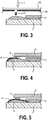
- Fig. 3 illustrates the application of a conductive protective layer to a contact pad using the method according to the invention.
- the contact pad 4 can have been applied by printing a band or strip of silver ink, and may have a width of about 0.5 ⁇ m - 20 ⁇ m.
- an organic layer 2 has been applied to partially cover the contact pad 4.
- a polyethylene carrier foil 62 is positioned above the contact pad 4 such that a transfer layer 60 - for example a thin coating of chromium or molybdenum - is facing towards the contact pad 4 and the organic light-emitting layer 2.
- the carrier foil is preferably positioned so that the transfer layer 60 is in direct contact with the organic layer 2, but for the sake of clarity, they are shown at a distance from each other in this diagram.
- the transfer layer 60 can have a coating thickness of only a few micrometers.
- a pulsed laser system for example a nanosecond UV laser is controlled so that a beam of laser light L is directed through the carrier foil 62 so that it locally heats the metal of the transfer layer 60 at a specific location above the contact pad 4.
- the metal vapourises a local pressure builds up between the carrier foil 62 and the molten metal. Due to the expansion of gas, a metal droplet 61 is accelerated and ejected towards to land on the contact pad 4 beneath. When the metal droplet 61 hits the contact pad 4 it adheres to its surface.
- This process is repeated to obtain a metal line from a series of individual metal droplets for the desired coverage of the contact pad 4.
- Typical layer thicknesses are in the order of a few micrometers down to some hundred nanometers.
- the achievable conductivities are typically greater by a factor of seven than the bulk resistivity of the bulk material used.
- Fig. 4 shows a cross-section of an outer region of an OLED device obtained using the method according to a first embodiment of the invention, in which the conductive protective layer 6 is applied on the outer region of the contact pad 4.
- an adhesive 5 is applied along the border between the conductive protective layer 6 and the exposed contact pad 4.
- the adhesive 5 could be applied to lie just inside the edge of the conductive protective layer 6, without touching the contact pad surface.
- the cover lid 3 is then put into place and the exposed contact pad 4, i.e. the surface not covered by the conductive protective layer 6, is effectively protected from the corrosive effects of the atmosphere.
- Fig. 5 shows a cross-section of an outer region of an OLED device obtained using the method according to a second embodiment of the invention, in which the conductive protective layer 6 is applied to cover the entire contact pad 4, and the adhesive is applied onto the conductive protective layer 6.
- Fig. 6 shows a cross-section of an outer region of an OLED device obtained using the method according to a comparative example, in which the contact pad 4 is narrower than in the realisations described above.
- the conductive protective layer 6 is applied adjacent to the narrow contact pad 4, and the adhesive 5 is applied along the border between the conductive protective layer 6 and the contact pad 4.
- the contact pads can be isolated using any combination of the techniques described above.
- the realisation of Fig. 4 could be used for the larger contact pad (often the cathode), while the shorter contact pad could be realised as shown in Fig. 6 .
- the realisation shown in Fig, 5 might be preferred on account of its straightforwardness.
- the realisation of Fig. 4 might be preferred since it combines a low material consumption with an optimal isolation from the harmful effects of the environment and in no way detracts from the conductivity of the contact pads.
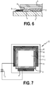
- Fig. 7 shows a plan view of an OLED device 10 manufactured using the method according to the invention described in Fig. 4 or Fig. 6 above.
- Contact pads 4 for an anode and cathode are applied - for example as printed metal lines - around the perimeter of a substrate 1.
- a thin conductive protective layer 6 is applied in an LMT process to coat the parts of the contact pads 4 that would lie outside an adhesive line 5, or to lie adjacent to narrower contact pads 4.
- a cover lid 3 is placed on top of the adhesive line 5, which together act as a sealant to encapsulate the OLED 10 and protect the organic layer 2.
- the contact pads 4 are protected from corrosion by the conductive protective layer 6.
Landscapes
- Engineering & Computer Science (AREA)
- Physics & Mathematics (AREA)
- Optics & Photonics (AREA)
- Manufacturing & Machinery (AREA)
- Microelectronics & Electronic Packaging (AREA)
- Electroluminescent Light Sources (AREA)
Claims (6)
- Verfahren zum Herstellen einer OLED-Vorrichtung (10), wobei das Verfahren umfasst:- Auftragen einer Anzahl von leitfähigen Streifen (4) als Anoden- und Kathodenkontaktpads für eine Anode und Kathode der OLED-Vorrichtung auf ein Substrat (1) unter Definition einer durch die leitfähigen Streifen begrenzten Region;- Abscheiden einer elektrolumineszierenden organischen Schicht (2) auf das Substrat (1) innerhalb der durch die leitfähigen Streifen (4) begrenzten Region;- Auftragen eines Dichtungsmittels auf die leitfähigen Streifen (4), um die OLED-Vorrichtung (1O) einzukapseln; und- Abscheiden einer leitfähigen Schutzschicht (6) zumindest teilweise auf jeden leitfähigen Streifen (4), so dass eine Oberfläche jedes leitfähigen Streifens (4) außerhalb des Dichtungsmittels vor schädlichen Umwelteinflüssen geschützt ist, wobei der Schritt des Abscheidens der leitfähigen Schutzschicht (6) Transferieren eines Teils der Transferschicht (60) oder einer Sequenz von Transferschichten (60) von einem Träger (62) umfasst.
- Verfahren nach Anspruch 1, wobei der Träger (62) eine Kunststofffolie (62) umfasst.
- Verfahren nach Anspruch 1, wobei der Schritt des Abscheidens der leitfähigen Schutzschicht (6) auf jeden leitfähigen Streifen (4) Durchführen eines Lasermassentransfers umfasst, um einen Teil der Transferschicht (60) vom Träger (62) auf den leitfähigen Streifen (4) zu transferieren.
- Verfahren nach Anspruch 3, wobei der Schritt des Durchführens eines Lasermassentransfers Deponieren von Energie an einer spezifischen Stelle in der Transferschicht (60) umfasst, um zu bewirken, dass die Transferschicht (60) zumindest teilweise auf den leitfähigen Streifen (4) transferiert wird.
- Verfahren nach einem der Ansprüche 1 bis 4, wobei der Träger (62) in Bezug auf die organische Schicht (2) so positioniert wird, dass die Transferschicht (60) mit der organischen Schicht (2) in direktem Kontakt steht.
- Verfahren nach einem der Ansprüche 1 bis 4, wobei der Schritt des Abscheidens der leitfähigen Schutzschicht (6) auf jeden leitfähigen Streifen (4) vor dem Schritt des Einkapselns der OLED-Vorrichtung (10) erfolgt.
Priority Applications (1)
| Application Number | Priority Date | Filing Date | Title |
|---|---|---|---|
| EP11744090.9A EP2593980B1 (de) | 2010-07-16 | 2011-07-11 | Verfahren zur herstellung einer oled-vorrichtung |
Applications Claiming Priority (3)
| Application Number | Priority Date | Filing Date | Title |
|---|---|---|---|
| EP10169821 | 2010-07-16 | ||
| EP11744090.9A EP2593980B1 (de) | 2010-07-16 | 2011-07-11 | Verfahren zur herstellung einer oled-vorrichtung |
| PCT/IB2011/053071 WO2012007893A1 (en) | 2010-07-16 | 2011-07-11 | An oled device and a method of manufacturing the same |
Publications (2)
| Publication Number | Publication Date |
|---|---|
| EP2593980A1 EP2593980A1 (de) | 2013-05-22 |
| EP2593980B1 true EP2593980B1 (de) | 2019-03-27 |
Family
ID=44544293
Family Applications (1)
| Application Number | Title | Priority Date | Filing Date |
|---|---|---|---|
| EP11744090.9A Not-in-force EP2593980B1 (de) | 2010-07-16 | 2011-07-11 | Verfahren zur herstellung einer oled-vorrichtung |
Country Status (6)
| Country | Link |
|---|---|
| US (1) | US8829787B2 (de) |
| EP (1) | EP2593980B1 (de) |
| JP (1) | JP5892707B2 (de) |
| KR (1) | KR101947194B1 (de) |
| CN (1) | CN102986053B (de) |
| WO (1) | WO2012007893A1 (de) |
Families Citing this family (5)
| Publication number | Priority date | Publication date | Assignee | Title |
|---|---|---|---|---|
| US9692008B2 (en) * | 2013-06-11 | 2017-06-27 | Sharp Kabushiki Kaisha | Organic electroluminescent display device |
| FR3017996A1 (fr) * | 2014-02-25 | 2015-08-28 | Commissariat Energie Atomique | Dispositif a composant electronique |
| KR102422061B1 (ko) | 2017-11-28 | 2022-07-18 | 엘지디스플레이 주식회사 | Oled 조명 장치 |
| KR102338064B1 (ko) | 2021-06-11 | 2021-12-13 | 주식회사 올레드링크 | Oled 패널 제조방법 |
| KR102337855B1 (ko) | 2021-09-03 | 2021-12-13 | 주식회사 올레드링크 | 개선된 증착 효과를 가지는 oled 패널 제조방법 |
Citations (2)
| Publication number | Priority date | Publication date | Assignee | Title |
|---|---|---|---|---|
| US20080061683A1 (en) * | 2004-09-27 | 2008-03-13 | Koninklijke Philips Electronics, N.V. | Illumination System |
| WO2008135902A2 (en) * | 2007-05-02 | 2008-11-13 | Philips Intellectual Property & Standards Gmbh | Method for manufacturing an oled device and such an oled device |
Family Cites Families (20)
| Publication number | Priority date | Publication date | Assignee | Title |
|---|---|---|---|---|
| JP3860793B2 (ja) * | 2000-11-08 | 2006-12-20 | コーニンクレッカ フィリップス エレクトロニクス エヌ ヴィ | 電気光学装置 |
| JP4551592B2 (ja) * | 2001-08-14 | 2010-09-29 | パイオニア株式会社 | 配線付き基体 |
| JP2003272832A (ja) * | 2002-03-13 | 2003-09-26 | Denso Corp | 有機el素子およびその製造方法 |
| JP2003297584A (ja) * | 2002-04-04 | 2003-10-17 | Asahi Glass Co Ltd | 配線付き基体形成用積層体、配線付き基体およびその形成方法 |
| JP4469126B2 (ja) * | 2002-06-14 | 2010-05-26 | 龍男 内田 | ディスプレイとそれに用いる配線基板 |
| JP2004047316A (ja) * | 2002-07-12 | 2004-02-12 | Sharp Corp | 有機led素子とその製造方法および表示装置 |
| US7169461B2 (en) * | 2002-10-17 | 2007-01-30 | Asahi Glass Company, Limited | Laminate, a substrate with wires, an organic EL display element, a connection terminal for the organic EL display element and a method for producing each |
| JP3649238B2 (ja) * | 2002-10-17 | 2005-05-18 | 旭硝子株式会社 | 積層体、配線付き基体、有機el表示素子、有機el表示素子の接続端子及びそれらの製造方法 |
| JP2005305714A (ja) * | 2004-04-19 | 2005-11-04 | Asahi Glass Co Ltd | 配線付き基体形成用積層体とその形成方法および配線付き基体 |
| KR100647677B1 (ko) * | 2005-02-04 | 2006-11-23 | 삼성에스디아이 주식회사 | 금속 보강층을 포함하는 유기 전계 발광 소자 및 그제조방법 |
| FR2904508B1 (fr) * | 2006-07-28 | 2014-08-22 | Saint Gobain | Dispositif electroluminescent encapsule |
| KR20070050804A (ko) * | 2006-08-28 | 2007-05-16 | 주식회사 대우일렉트로닉스 | 오엘이디 디스플레이 패널 |
| WO2008040323A2 (de) * | 2006-09-29 | 2008-04-10 | Osram Opto Semiconductors Gmbh | Organisches leuchtmittel und beleuchtungseinrichtung |
| JP2008166232A (ja) | 2007-01-05 | 2008-07-17 | Fuji Electric Holdings Co Ltd | 有機elディスプレイの製造方法 |
| US8222635B2 (en) * | 2007-03-20 | 2012-07-17 | Otb Solar B.V. | Method for manufacturing an organic light emitting device as well as such a device |
| JP2009076437A (ja) * | 2007-08-31 | 2009-04-09 | Toshiba Matsushita Display Technology Co Ltd | 表示装置 |
| JP4950870B2 (ja) * | 2007-12-21 | 2012-06-13 | ローム株式会社 | 有機発光装置 |
| JP5049213B2 (ja) * | 2008-07-08 | 2012-10-17 | 株式会社ジャパンディスプレイイースト | 有機elパネルおよびその製造方法 |
| US20100118243A1 (en) * | 2008-11-12 | 2010-05-13 | Debasis Majumdar | Polymeric conductive donor and transfer method |
| JP4849279B2 (ja) * | 2009-05-28 | 2012-01-11 | Tdk株式会社 | 有機el表示装置 |
-
2011
- 2011-07-11 KR KR1020137003869A patent/KR101947194B1/ko active IP Right Grant
- 2011-07-11 JP JP2013519198A patent/JP5892707B2/ja not_active Expired - Fee Related
- 2011-07-11 US US13/810,261 patent/US8829787B2/en not_active Expired - Fee Related
- 2011-07-11 CN CN201180035011.8A patent/CN102986053B/zh not_active Expired - Fee Related
- 2011-07-11 WO PCT/IB2011/053071 patent/WO2012007893A1/en active Application Filing
- 2011-07-11 EP EP11744090.9A patent/EP2593980B1/de not_active Not-in-force
Patent Citations (2)
| Publication number | Priority date | Publication date | Assignee | Title |
|---|---|---|---|---|
| US20080061683A1 (en) * | 2004-09-27 | 2008-03-13 | Koninklijke Philips Electronics, N.V. | Illumination System |
| WO2008135902A2 (en) * | 2007-05-02 | 2008-11-13 | Philips Intellectual Property & Standards Gmbh | Method for manufacturing an oled device and such an oled device |
Non-Patent Citations (1)
| Title |
|---|
| LOGOTHETIDIS ET AL: "Flexible organic electronic devices: Materials, process and applications", MATERIALS SCIENCE AND ENGINEERING: B, ELSEVIER, AMSTERDAM, NL, vol. 152, no. 1-3, 25 August 2008 (2008-08-25), pages 96 - 104, XP025609287, ISSN: 0921-5107, [retrieved on 20080709], DOI: 10.1016/J.MSEB.2008.06.009 * |
Also Published As
| Publication number | Publication date |
|---|---|
| KR101947194B1 (ko) | 2019-02-12 |
| CN102986053B (zh) | 2016-03-02 |
| CN102986053A (zh) | 2013-03-20 |
| EP2593980A1 (de) | 2013-05-22 |
| JP2013534706A (ja) | 2013-09-05 |
| WO2012007893A1 (en) | 2012-01-19 |
| US8829787B2 (en) | 2014-09-09 |
| KR20130041945A (ko) | 2013-04-25 |
| US20130119858A1 (en) | 2013-05-16 |
| JP5892707B2 (ja) | 2016-03-23 |
Similar Documents
| Publication | Publication Date | Title |
|---|---|---|
| EP2593980B1 (de) | Verfahren zur herstellung einer oled-vorrichtung | |
| KR100796129B1 (ko) | 유기 전계 발광 표시장치 및 그 제조방법 | |
| US8653544B2 (en) | OLEDs connected in series | |
| EP3035404A1 (de) | Barrierenfolie mit elektrischem Stromkreis | |
| US20130143337A1 (en) | Organic electroluminescent device | |
| WO2013114295A1 (en) | Oled device and manufacture thereof | |
| CN102308409A (zh) | 电致发光装置 | |
| CN103219474A (zh) | 一种基板封装方法 | |
| EP2550693B1 (de) | Verfahren zur herstellung einer oled-vorrichtung mit räumlich isolierten lichtemittierenden bereichen | |
| KR102239286B1 (ko) | 유기 발광 표시 장치용 봉지 필름 및 이를 이용한 유기 발광 표시 장치 | |
| JP2012146661A (ja) | インクジェット印刷を用いてラッカー層を形成する方法 | |
| US9515293B2 (en) | OLED encapsulated in a full-wafer adhesive having a perforated cover | |
| US20090294157A1 (en) | Electro-optic device and method for manufacturing the same | |
| EP2135308B1 (de) | Verfahren zur herstellung eines organischen leuchtbauelements sowie solches bauelement | |
| WO2011064692A1 (en) | Organic electroluminescent devices | |
| JP5363246B2 (ja) | 有機エレクトロルミネッセンス装置及びその製造方法 | |
| CN111095593A (zh) | 用于无掩模oled沉积和制造的方法 | |
| JP2018200843A (ja) | 有機el装置の製造方法 | |
| KR20080063824A (ko) | 전압 작동층 장치 및 그 제조 방법 | |
| JP2015153740A (ja) | 発光装置及び発光装置の製造方法 | |
| WO2012007875A1 (en) | Oled device and method of manufacturing the same |
Legal Events
| Date | Code | Title | Description |
|---|---|---|---|
| PUAI | Public reference made under article 153(3) epc to a published international application that has entered the european phase |
Free format text: ORIGINAL CODE: 0009012 |
|
| 17P | Request for examination filed |
Effective date: 20130218 |
|
| AK | Designated contracting states |
Kind code of ref document: A1 Designated state(s): AL AT BE BG CH CY CZ DE DK EE ES FI FR GB GR HR HU IE IS IT LI LT LU LV MC MK MT NL NO PL PT RO RS SE SI SK SM TR |
|
| RAP1 | Party data changed (applicant data changed or rights of an application transferred) |
Owner name: PHILIPS INTELLECTUAL PROPERTY & STANDARDS GMBH Owner name: KONINKLIJKE PHILIPS N.V. |
|
| DAX | Request for extension of the european patent (deleted) | ||
| 17Q | First examination report despatched |
Effective date: 20160225 |
|
| RAP1 | Party data changed (applicant data changed or rights of an application transferred) |
Owner name: OLEDWORKS GMBH |
|
| STAA | Information on the status of an ep patent application or granted ep patent |
Free format text: STATUS: EXAMINATION IS IN PROGRESS |
|
| RIN1 | Information on inventor provided before grant (corrected) |
Inventor name: SCHWAB, HOLGER |
|
| GRAP | Despatch of communication of intention to grant a patent |
Free format text: ORIGINAL CODE: EPIDOSNIGR1 |
|
| STAA | Information on the status of an ep patent application or granted ep patent |
Free format text: STATUS: GRANT OF PATENT IS INTENDED |
|
| INTG | Intention to grant announced |
Effective date: 20181204 |
|
| GRAS | Grant fee paid |
Free format text: ORIGINAL CODE: EPIDOSNIGR3 |
|
| GRAA | (expected) grant |
Free format text: ORIGINAL CODE: 0009210 |
|
| STAA | Information on the status of an ep patent application or granted ep patent |
Free format text: STATUS: THE PATENT HAS BEEN GRANTED |
|
| AK | Designated contracting states |
Kind code of ref document: B1 Designated state(s): AL AT BE BG CH CY CZ DE DK EE ES FI FR GB GR HR HU IE IS IT LI LT LU LV MC MK MT NL NO PL PT RO RS SE SI SK SM TR |
|
| RAP1 | Party data changed (applicant data changed or rights of an application transferred) |
Owner name: OLEDWORKS GMBH |
|
| REG | Reference to a national code |
Ref country code: GB Ref legal event code: FG4D |
|
| REG | Reference to a national code |
Ref country code: CH Ref legal event code: EP |
|
| REG | Reference to a national code |
Ref country code: AT Ref legal event code: REF Ref document number: 1114092 Country of ref document: AT Kind code of ref document: T Effective date: 20190415 |
|
| REG | Reference to a national code |
Ref country code: IE Ref legal event code: FG4D |
|
| REG | Reference to a national code |
Ref country code: DE Ref legal event code: R096 Ref document number: 602011057523 Country of ref document: DE |
|
| PG25 | Lapsed in a contracting state [announced via postgrant information from national office to epo] |
Ref country code: LT Free format text: LAPSE BECAUSE OF FAILURE TO SUBMIT A TRANSLATION OF THE DESCRIPTION OR TO PAY THE FEE WITHIN THE PRESCRIBED TIME-LIMIT Effective date: 20190327 Ref country code: FI Free format text: LAPSE BECAUSE OF FAILURE TO SUBMIT A TRANSLATION OF THE DESCRIPTION OR TO PAY THE FEE WITHIN THE PRESCRIBED TIME-LIMIT Effective date: 20190327 Ref country code: SE Free format text: LAPSE BECAUSE OF FAILURE TO SUBMIT A TRANSLATION OF THE DESCRIPTION OR TO PAY THE FEE WITHIN THE PRESCRIBED TIME-LIMIT Effective date: 20190327 Ref country code: NO Free format text: LAPSE BECAUSE OF FAILURE TO SUBMIT A TRANSLATION OF THE DESCRIPTION OR TO PAY THE FEE WITHIN THE PRESCRIBED TIME-LIMIT Effective date: 20190627 |
|
| REG | Reference to a national code |
Ref country code: NL Ref legal event code: MP Effective date: 20190327 |
|
| PG25 | Lapsed in a contracting state [announced via postgrant information from national office to epo] |
Ref country code: LV Free format text: LAPSE BECAUSE OF FAILURE TO SUBMIT A TRANSLATION OF THE DESCRIPTION OR TO PAY THE FEE WITHIN THE PRESCRIBED TIME-LIMIT Effective date: 20190327 Ref country code: HR Free format text: LAPSE BECAUSE OF FAILURE TO SUBMIT A TRANSLATION OF THE DESCRIPTION OR TO PAY THE FEE WITHIN THE PRESCRIBED TIME-LIMIT Effective date: 20190327 Ref country code: GR Free format text: LAPSE BECAUSE OF FAILURE TO SUBMIT A TRANSLATION OF THE DESCRIPTION OR TO PAY THE FEE WITHIN THE PRESCRIBED TIME-LIMIT Effective date: 20190628 Ref country code: BG Free format text: LAPSE BECAUSE OF FAILURE TO SUBMIT A TRANSLATION OF THE DESCRIPTION OR TO PAY THE FEE WITHIN THE PRESCRIBED TIME-LIMIT Effective date: 20190627 Ref country code: RS Free format text: LAPSE BECAUSE OF FAILURE TO SUBMIT A TRANSLATION OF THE DESCRIPTION OR TO PAY THE FEE WITHIN THE PRESCRIBED TIME-LIMIT Effective date: 20190327 Ref country code: NL Free format text: LAPSE BECAUSE OF FAILURE TO SUBMIT A TRANSLATION OF THE DESCRIPTION OR TO PAY THE FEE WITHIN THE PRESCRIBED TIME-LIMIT Effective date: 20190327 |
|
| REG | Reference to a national code |
Ref country code: AT Ref legal event code: MK05 Ref document number: 1114092 Country of ref document: AT Kind code of ref document: T Effective date: 20190327 |
|
| PG25 | Lapsed in a contracting state [announced via postgrant information from national office to epo] |
Ref country code: ES Free format text: LAPSE BECAUSE OF FAILURE TO SUBMIT A TRANSLATION OF THE DESCRIPTION OR TO PAY THE FEE WITHIN THE PRESCRIBED TIME-LIMIT Effective date: 20190327 Ref country code: PT Free format text: LAPSE BECAUSE OF FAILURE TO SUBMIT A TRANSLATION OF THE DESCRIPTION OR TO PAY THE FEE WITHIN THE PRESCRIBED TIME-LIMIT Effective date: 20190727 Ref country code: AL Free format text: LAPSE BECAUSE OF FAILURE TO SUBMIT A TRANSLATION OF THE DESCRIPTION OR TO PAY THE FEE WITHIN THE PRESCRIBED TIME-LIMIT Effective date: 20190327 Ref country code: CZ Free format text: LAPSE BECAUSE OF FAILURE TO SUBMIT A TRANSLATION OF THE DESCRIPTION OR TO PAY THE FEE WITHIN THE PRESCRIBED TIME-LIMIT Effective date: 20190327 Ref country code: RO Free format text: LAPSE BECAUSE OF FAILURE TO SUBMIT A TRANSLATION OF THE DESCRIPTION OR TO PAY THE FEE WITHIN THE PRESCRIBED TIME-LIMIT Effective date: 20190327 Ref country code: SK Free format text: LAPSE BECAUSE OF FAILURE TO SUBMIT A TRANSLATION OF THE DESCRIPTION OR TO PAY THE FEE WITHIN THE PRESCRIBED TIME-LIMIT Effective date: 20190327 Ref country code: IT Free format text: LAPSE BECAUSE OF FAILURE TO SUBMIT A TRANSLATION OF THE DESCRIPTION OR TO PAY THE FEE WITHIN THE PRESCRIBED TIME-LIMIT Effective date: 20190327 Ref country code: EE Free format text: LAPSE BECAUSE OF FAILURE TO SUBMIT A TRANSLATION OF THE DESCRIPTION OR TO PAY THE FEE WITHIN THE PRESCRIBED TIME-LIMIT Effective date: 20190327 |
|
| PG25 | Lapsed in a contracting state [announced via postgrant information from national office to epo] |
Ref country code: SM Free format text: LAPSE BECAUSE OF FAILURE TO SUBMIT A TRANSLATION OF THE DESCRIPTION OR TO PAY THE FEE WITHIN THE PRESCRIBED TIME-LIMIT Effective date: 20190327 Ref country code: PL Free format text: LAPSE BECAUSE OF FAILURE TO SUBMIT A TRANSLATION OF THE DESCRIPTION OR TO PAY THE FEE WITHIN THE PRESCRIBED TIME-LIMIT Effective date: 20190327 |
|
| PG25 | Lapsed in a contracting state [announced via postgrant information from national office to epo] |
Ref country code: IS Free format text: LAPSE BECAUSE OF FAILURE TO SUBMIT A TRANSLATION OF THE DESCRIPTION OR TO PAY THE FEE WITHIN THE PRESCRIBED TIME-LIMIT Effective date: 20190727 Ref country code: AT Free format text: LAPSE BECAUSE OF FAILURE TO SUBMIT A TRANSLATION OF THE DESCRIPTION OR TO PAY THE FEE WITHIN THE PRESCRIBED TIME-LIMIT Effective date: 20190327 |
|
| REG | Reference to a national code |
Ref country code: DE Ref legal event code: R097 Ref document number: 602011057523 Country of ref document: DE |
|
| PG25 | Lapsed in a contracting state [announced via postgrant information from national office to epo] |
Ref country code: DK Free format text: LAPSE BECAUSE OF FAILURE TO SUBMIT A TRANSLATION OF THE DESCRIPTION OR TO PAY THE FEE WITHIN THE PRESCRIBED TIME-LIMIT Effective date: 20190327 |
|
| PLBE | No opposition filed within time limit |
Free format text: ORIGINAL CODE: 0009261 |
|
| STAA | Information on the status of an ep patent application or granted ep patent |
Free format text: STATUS: NO OPPOSITION FILED WITHIN TIME LIMIT |
|
| PG25 | Lapsed in a contracting state [announced via postgrant information from national office to epo] |
Ref country code: MC Free format text: LAPSE BECAUSE OF FAILURE TO SUBMIT A TRANSLATION OF THE DESCRIPTION OR TO PAY THE FEE WITHIN THE PRESCRIBED TIME-LIMIT Effective date: 20190327 Ref country code: SI Free format text: LAPSE BECAUSE OF FAILURE TO SUBMIT A TRANSLATION OF THE DESCRIPTION OR TO PAY THE FEE WITHIN THE PRESCRIBED TIME-LIMIT Effective date: 20190327 |
|
| REG | Reference to a national code |
Ref country code: CH Ref legal event code: PL |
|
| 26N | No opposition filed |
Effective date: 20200103 |
|
| PG25 | Lapsed in a contracting state [announced via postgrant information from national office to epo] |
Ref country code: TR Free format text: LAPSE BECAUSE OF FAILURE TO SUBMIT A TRANSLATION OF THE DESCRIPTION OR TO PAY THE FEE WITHIN THE PRESCRIBED TIME-LIMIT Effective date: 20190327 |
|
| REG | Reference to a national code |
Ref country code: BE Ref legal event code: MM Effective date: 20190731 |
|
| PG25 | Lapsed in a contracting state [announced via postgrant information from national office to epo] |
Ref country code: CH Free format text: LAPSE BECAUSE OF NON-PAYMENT OF DUE FEES Effective date: 20190731 Ref country code: LI Free format text: LAPSE BECAUSE OF NON-PAYMENT OF DUE FEES Effective date: 20190731 Ref country code: LU Free format text: LAPSE BECAUSE OF NON-PAYMENT OF DUE FEES Effective date: 20190711 Ref country code: BE Free format text: LAPSE BECAUSE OF NON-PAYMENT OF DUE FEES Effective date: 20190731 |
|
| PG25 | Lapsed in a contracting state [announced via postgrant information from national office to epo] |
Ref country code: IE Free format text: LAPSE BECAUSE OF NON-PAYMENT OF DUE FEES Effective date: 20190711 |
|
| PGFP | Annual fee paid to national office [announced via postgrant information from national office to epo] |
Ref country code: FR Payment date: 20200611 Year of fee payment: 10 |
|
| PGFP | Annual fee paid to national office [announced via postgrant information from national office to epo] |
Ref country code: GB Payment date: 20200701 Year of fee payment: 10 Ref country code: DE Payment date: 20200630 Year of fee payment: 10 |
|
| PG25 | Lapsed in a contracting state [announced via postgrant information from national office to epo] |
Ref country code: CY Free format text: LAPSE BECAUSE OF FAILURE TO SUBMIT A TRANSLATION OF THE DESCRIPTION OR TO PAY THE FEE WITHIN THE PRESCRIBED TIME-LIMIT Effective date: 20190327 |
|
| PG25 | Lapsed in a contracting state [announced via postgrant information from national office to epo] |
Ref country code: MT Free format text: LAPSE BECAUSE OF FAILURE TO SUBMIT A TRANSLATION OF THE DESCRIPTION OR TO PAY THE FEE WITHIN THE PRESCRIBED TIME-LIMIT Effective date: 20190327 Ref country code: HU Free format text: LAPSE BECAUSE OF FAILURE TO SUBMIT A TRANSLATION OF THE DESCRIPTION OR TO PAY THE FEE WITHIN THE PRESCRIBED TIME-LIMIT; INVALID AB INITIO Effective date: 20110711 |
|
| REG | Reference to a national code |
Ref country code: DE Ref legal event code: R119 Ref document number: 602011057523 Country of ref document: DE |
|
| GBPC | Gb: european patent ceased through non-payment of renewal fee |
Effective date: 20210711 |
|
| PG25 | Lapsed in a contracting state [announced via postgrant information from national office to epo] |
Ref country code: GB Free format text: LAPSE BECAUSE OF NON-PAYMENT OF DUE FEES Effective date: 20210711 Ref country code: DE Free format text: LAPSE BECAUSE OF NON-PAYMENT OF DUE FEES Effective date: 20220201 |
|
| PG25 | Lapsed in a contracting state [announced via postgrant information from national office to epo] |
Ref country code: FR Free format text: LAPSE BECAUSE OF NON-PAYMENT OF DUE FEES Effective date: 20210731 |
|
| PG25 | Lapsed in a contracting state [announced via postgrant information from national office to epo] |
Ref country code: MK Free format text: LAPSE BECAUSE OF FAILURE TO SUBMIT A TRANSLATION OF THE DESCRIPTION OR TO PAY THE FEE WITHIN THE PRESCRIBED TIME-LIMIT Effective date: 20190327 |