EP2584700A2 - Sperrschaltung und Anzeigevorrichtung - Google Patents
Sperrschaltung und Anzeigevorrichtung Download PDFInfo
- Publication number
- EP2584700A2 EP2584700A2 EP12188809.3A EP12188809A EP2584700A2 EP 2584700 A2 EP2584700 A2 EP 2584700A2 EP 12188809 A EP12188809 A EP 12188809A EP 2584700 A2 EP2584700 A2 EP 2584700A2
- Authority
- EP
- European Patent Office
- Prior art keywords
- voltage
- time
- transistor
- voltage level
- electrode
- Prior art date
- Legal status (The legal status is an assumption and is not a legal conclusion. Google has not performed a legal analysis and makes no representation as to the accuracy of the status listed.)
- Withdrawn
Links
Images







Classifications
-
- G—PHYSICS
- G09—EDUCATION; CRYPTOGRAPHY; DISPLAY; ADVERTISING; SEALS
- G09G—ARRANGEMENTS OR CIRCUITS FOR CONTROL OF INDICATING DEVICES USING STATIC MEANS TO PRESENT VARIABLE INFORMATION
- G09G3/00—Control arrangements or circuits, of interest only in connection with visual indicators other than cathode-ray tubes
- G09G3/20—Control arrangements or circuits, of interest only in connection with visual indicators other than cathode-ray tubes for presentation of an assembly of a number of characters, e.g. a page, by composing the assembly by combination of individual elements arranged in a matrix no fixed position being assigned to or needed to be assigned to the individual characters or partial characters
-
- H—ELECTRICITY
- H03—ELECTRONIC CIRCUITRY
- H03K—PULSE TECHNIQUE
- H03K5/00—Manipulating of pulses not covered by one of the other main groups of this subclass
- H03K5/153—Arrangements in which a pulse is delivered at the instant when a predetermined characteristic of an input signal is present or at a fixed time interval after this instant
-
- G—PHYSICS
- G09—EDUCATION; CRYPTOGRAPHY; DISPLAY; ADVERTISING; SEALS
- G09G—ARRANGEMENTS OR CIRCUITS FOR CONTROL OF INDICATING DEVICES USING STATIC MEANS TO PRESENT VARIABLE INFORMATION
- G09G3/00—Control arrangements or circuits, of interest only in connection with visual indicators other than cathode-ray tubes
- G09G3/20—Control arrangements or circuits, of interest only in connection with visual indicators other than cathode-ray tubes for presentation of an assembly of a number of characters, e.g. a page, by composing the assembly by combination of individual elements arranged in a matrix no fixed position being assigned to or needed to be assigned to the individual characters or partial characters
- G09G3/2092—Details of a display terminals using a flat panel, the details relating to the control arrangement of the display terminal and to the interfaces thereto
-
- G—PHYSICS
- G09—EDUCATION; CRYPTOGRAPHY; DISPLAY; ADVERTISING; SEALS
- G09G—ARRANGEMENTS OR CIRCUITS FOR CONTROL OF INDICATING DEVICES USING STATIC MEANS TO PRESENT VARIABLE INFORMATION
- G09G3/00—Control arrangements or circuits, of interest only in connection with visual indicators other than cathode-ray tubes
- G09G3/20—Control arrangements or circuits, of interest only in connection with visual indicators other than cathode-ray tubes for presentation of an assembly of a number of characters, e.g. a page, by composing the assembly by combination of individual elements arranged in a matrix no fixed position being assigned to or needed to be assigned to the individual characters or partial characters
- G09G3/34—Control arrangements or circuits, of interest only in connection with visual indicators other than cathode-ray tubes for presentation of an assembly of a number of characters, e.g. a page, by composing the assembly by combination of individual elements arranged in a matrix no fixed position being assigned to or needed to be assigned to the individual characters or partial characters by control of light from an independent source
- G09G3/3433—Control arrangements or circuits, of interest only in connection with visual indicators other than cathode-ray tubes for presentation of an assembly of a number of characters, e.g. a page, by composing the assembly by combination of individual elements arranged in a matrix no fixed position being assigned to or needed to be assigned to the individual characters or partial characters by control of light from an independent source using light modulating elements actuated by an electric field and being other than liquid crystal devices and electrochromic devices
-
- H—ELECTRICITY
- H03—ELECTRONIC CIRCUITRY
- H03K—PULSE TECHNIQUE
- H03K3/00—Circuits for generating electric pulses; Monostable, bistable or multistable circuits
- H03K3/02—Generators characterised by the type of circuit or by the means used for producing pulses
- H03K3/353—Generators characterised by the type of circuit or by the means used for producing pulses by the use, as active elements, of field-effect transistors with internal or external positive feedback
- H03K3/356—Bistable circuits
-
- H—ELECTRICITY
- H03—ELECTRONIC CIRCUITRY
- H03K—PULSE TECHNIQUE
- H03K3/00—Circuits for generating electric pulses; Monostable, bistable or multistable circuits
- H03K3/02—Generators characterised by the type of circuit or by the means used for producing pulses
- H03K3/353—Generators characterised by the type of circuit or by the means used for producing pulses by the use, as active elements, of field-effect transistors with internal or external positive feedback
- H03K3/356—Bistable circuits
- H03K3/356104—Bistable circuits using complementary field-effect transistors
- H03K3/356113—Bistable circuits using complementary field-effect transistors using additional transistors in the input circuit
-
- G—PHYSICS
- G09—EDUCATION; CRYPTOGRAPHY; DISPLAY; ADVERTISING; SEALS
- G09G—ARRANGEMENTS OR CIRCUITS FOR CONTROL OF INDICATING DEVICES USING STATIC MEANS TO PRESENT VARIABLE INFORMATION
- G09G2310/00—Command of the display device
- G09G2310/02—Addressing, scanning or driving the display screen or processing steps related thereto
-
- G—PHYSICS
- G09—EDUCATION; CRYPTOGRAPHY; DISPLAY; ADVERTISING; SEALS
- G09G—ARRANGEMENTS OR CIRCUITS FOR CONTROL OF INDICATING DEVICES USING STATIC MEANS TO PRESENT VARIABLE INFORMATION
- G09G2310/00—Command of the display device
- G09G2310/02—Addressing, scanning or driving the display screen or processing steps related thereto
- G09G2310/0264—Details of driving circuits
-
- G—PHYSICS
- G09—EDUCATION; CRYPTOGRAPHY; DISPLAY; ADVERTISING; SEALS
- G09G—ARRANGEMENTS OR CIRCUITS FOR CONTROL OF INDICATING DEVICES USING STATIC MEANS TO PRESENT VARIABLE INFORMATION
- G09G2310/00—Command of the display device
- G09G2310/02—Addressing, scanning or driving the display screen or processing steps related thereto
- G09G2310/0264—Details of driving circuits
- G09G2310/0289—Details of voltage level shifters arranged for use in a driving circuit
-
- G—PHYSICS
- G09—EDUCATION; CRYPTOGRAPHY; DISPLAY; ADVERTISING; SEALS
- G09G—ARRANGEMENTS OR CIRCUITS FOR CONTROL OF INDICATING DEVICES USING STATIC MEANS TO PRESENT VARIABLE INFORMATION
- G09G2310/00—Command of the display device
- G09G2310/02—Addressing, scanning or driving the display screen or processing steps related thereto
- G09G2310/0264—Details of driving circuits
- G09G2310/0294—Details of sampling or holding circuits arranged for use in a driver for data electrodes
-
- G—PHYSICS
- G09—EDUCATION; CRYPTOGRAPHY; DISPLAY; ADVERTISING; SEALS
- G09G—ARRANGEMENTS OR CIRCUITS FOR CONTROL OF INDICATING DEVICES USING STATIC MEANS TO PRESENT VARIABLE INFORMATION
- G09G2310/00—Command of the display device
- G09G2310/08—Details of timing specific for flat panels, other than clock recovery
-
- G—PHYSICS
- G09—EDUCATION; CRYPTOGRAPHY; DISPLAY; ADVERTISING; SEALS
- G09G—ARRANGEMENTS OR CIRCUITS FOR CONTROL OF INDICATING DEVICES USING STATIC MEANS TO PRESENT VARIABLE INFORMATION
- G09G2320/00—Control of display operating conditions
- G09G2320/04—Maintaining the quality of display appearance
- G09G2320/043—Preventing or counteracting the effects of ageing
- G09G2320/045—Compensation of drifts in the characteristics of light emitting or modulating elements
-
- H—ELECTRICITY
- H03—ELECTRONIC CIRCUITRY
- H03K—PULSE TECHNIQUE
- H03K5/00—Manipulating of pulses not covered by one of the other main groups of this subclass
- H03K2005/00013—Delay, i.e. output pulse is delayed after input pulse and pulse length of output pulse is dependent on pulse length of input pulse
- H03K2005/00078—Fixed delay
-
- H—ELECTRICITY
- H03—ELECTRONIC CIRCUITRY
- H03K—PULSE TECHNIQUE
- H03K5/00—Manipulating of pulses not covered by one of the other main groups of this subclass
- H03K2005/00013—Delay, i.e. output pulse is delayed after input pulse and pulse length of output pulse is dependent on pulse length of input pulse
- H03K2005/0015—Layout of the delay element
- H03K2005/00195—Layout of the delay element using FET's
- H03K2005/00215—Layout of the delay element using FET's where the conduction path of multiple FET's is in parallel or in series, all having the same gate control
Definitions
- the present invention is related to a latch circuit and a display device.
- the present invention is related to a latch circuit which latches latch data in relatively short time intervals, and a display device which uses the latch circuit.
- a latch circuit is formed from a CMOS circuit.
- CMOS circuit For example, as is shown in Fig. 12 , a latch circuit which uses an n type MOS transistor (NMT93, NMT94) connected between a power supply line (LVDD) supplied with a VDD voltage and a power supply line (LGND) supplied with a GND voltage, and a p type MOS transistor (PMT95, PMT96) is commonly used.
- NMT93, NMT94 n type MOS transistor
- LGND power supply line
- PMT95, PMT96 p type MOS transistor
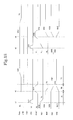
- Fig. 13 shows variance of a scanning pulse ( ⁇ G) applied to a scanning line (LD) shown in Fig. 12 , a latch control signal ( ⁇ AC1) applied to a latch control line (LAC) and evoltages of each node (N91, N92, N93, N94) in accordance with time elapse.
- ⁇ G scanning pulse
- LD scanning line
- LAC latch control line
- a voltage (data) on a signal line (LD) is a Low level (herein referred to as L level) voltage is explained.
- the voltage of the node N91 is a High level (herein referred to as H level) voltage VH3
- that of the node N92 is an H level voltage VDD
- that of the node N93 is an L level voltage GND
- that of the node N94 is an L level voltage VH4.
- the n type MOS transistor NMT92 is turned ON and the voltage of the node N94 becomes a voltage VL.
- the p type MOS transistor PMT95 and the n type MOS transistor NMT94 are turned ON
- the p type MOS transistor PMT96 and the n type MOS transistor NMT93 are turned OFF
- the voltage of the node N92 (output terminal (OUT2)) becomes a L level voltage GND
- the voltage of the node N91 is an L level voltage VL
- that of the node N92 is an L level voltage GND
- that of the node N93 is an H level voltage VDD
- that of the node N94 is an L level voltage VL.
- the n type MOS transistor NMT91 is turned ON, and a voltage (data: here a voltage VDH) on the signal line (LD) is input to a storage capacitance (CD). In this way, the voltage of the node N91 becomes a voltage VH3.
- the latch control signal ( ⁇ AC1) on the latch control line (LAC) changed from a L level voltage VL to a H level voltage VH2 at a time t4
- the n type MOS transistor (NMT92) is turned ON and the voltage of the node N94 becomes a voltage VH4.
- the n type MOS transistor (NMT93) and the p type MOS transistor (NMT96) are turned ON, the p type MOS transistor (PMT95) and the n type MOS transistor (NMT94) are turned OFF, the voltage of the node (N92) (output terminal (OUT2)) becomes a H level voltage VDD, and the voltage of the node (N93) (output terminal (OUT1)) becomes a L level voltage GND.
- a pixel circuit of a display (referred to below as a movable shutter type display) which electrically controls the position of a movable shutter (s) to display an image in accordance with output signals from two output terminals (OUT1, OUT2) of the latch circuit is a specific usage example of the latch circuit shown in Fig. 12 .
- a movable shutter type display is disclosed for example in Patent Document 1 (Japanese Laid Open Patent 2008-197668 ).
- the movable shutter (s) moves at a high speed in the direction of an electric field.
- the movable shutter (s) moves to the node N93.
- the movable shutter (s) moves at a high speed to the node N92.
- LSS is a movable shutter control line supplied with a shutter control signal ( ⁇ S).
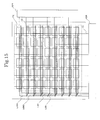
- Fig. 15 is a block diagram which shows an approximate structure of a movable shutter type display.
- a plurality of pixel circuits shown in Fig. 14 each corresponding to 1 pixel (PX) are arranged in 2 dimensions.
- the scanning line (LG) is arranged on each row of which signal is input to a vertical drive circuit (XDR).
- a signal line (LD) is arranged on each column of which signal is input to a horizontal drive circuit (YDR).
- Power supply lines (LVDD, LGND), the latch control line (LAC) and the movable shutter control line (LSS) are commonly arranged on each pixel to input signals to the horizontal drive circuit (YDR).
- a movable shutter type display shown in Fig. 15 data is programmed to each pixel on each row within a programming time period (TA in Fig. 13 ), and within a movable shutter state setting time period (TB in Fig. 13 ), the movable shutter (s) is made to move to the node N92 or the node N93 and an image is displayed in a display time period (TC in Fig. 13 ).
- a circuit configuration in which a latch circuit is configured of a CMOS circuit is currently widely used and has proven actual results.
- a latch circuit configured of the CMOS circuit shown in Fig. 12 for high voltage use for example, for use with a voltage where a potential difference between a voltage VDD and a voltage GND is 20V or more
- MOS transistor in which polycrystalline silicon (polysilicon) is used for a semiconductor layer it is assumed that the characteristics of a thin film transistor deteriorate due to a drain avalanche effect and doubts concerning reliability arise.
- the present invention was performed in order to solve these conventional technological problems.
- the aim of the present invention is to provide a latch circuit which is capable of controlling a drain avalanche effect and improving reliability, and a display device which uses this latch circuit.
- the aim of the present invention and other aims and new characteristics are made clear with reference to the descriptions of the present specification and attached drawings.
- the first aspect of the present invention is a latch circuit for holding and latching data when a scanning voltage is input.
- the circuit comprises an input transistor having first and second electrodes and a gate, the first electrode being applied with a voltage corresponding to "0" or "1", the input transistor outputting the voltage from the second electrode when the scanning voltage is input to the gate, a retention capacitance retaining a voltage output by the input transistor , and having a first electrode and a second electrode, the second electrode being applied with a capacitance control signal and the first electrode being connected to a second electrode of the input transistor, a first transistor which is one of n type and p type transistors having a gate connected to the second electrode of the input transistor, a first electrode applied with a first latch control signal and a second electrode connected to a first output terminal and a second transistor which is the other of n type and p type transistors having a gate connected to the second electrode of the first transistor, a first electrode input with a second latch control signal and a second electrode connected to a second
- voltage levels of the capacitance control signal and the first latch control signal and the second latch control signal are respectively changed at a certain timing, so that a voltage of the first output terminal and a voltage of the second output terminal are changed to a voltage corresponding to "0" or "1" and latched.
- the voltage of the second latch control signal may be a second voltage level in a time period up to a time t1 after a voltage corresponding to "0" data or "1" data is retained in the retention capacitance, changed to a first voltage level from the second voltage level at the time t1, and changed to the second voltage level from the first voltage level at a time t7
- the voltage of the capacitance control signal may be the second voltage level in a time period up to a time t2, changed to the second voltage level from the first voltage level at the time t2, and changed to the first voltage level from the second voltage level at a time t4
- the voltage of the first latch control signal may be an intermediate voltage level between the first voltage level and the second voltage level in a time period up to a time t3, changed to the second voltage level from the intermediate voltage level at the time t3, changed to the first voltage level from the second
- the first transistor is turned OFF before the time t3, turned ON at the time t3, turned OFF at the time t4, turned ON or OFF in accordance with a voltage stored in the storage capacitance at the time t5, and turned OFF after t6, the second transistor is turned ON at the time t4 by the first transistor being turned ON at the time t3m, turned OFF at the time t4, and turned ON when the first transistor is turned ON at the time t5, or turned OFF when the first transistor is turned OFF at the time t5.
- the first transistor is turned ON at the time t3, the voltage of the first output terminal is changed to the intermediate voltage level at the time t3, and then changed to the second voltage level at the time t4, is maintained at the first voltage level after being changed to the first voltage level in the case where the first transistor is turned ON at the time t5.
- the second transistor is turned ON at the time t3, the voltage of the second output terminal is changed to the first voltage level , maintained at a voltage of a second voltage level after being changed to the second voltage level at a time t7 in the case where the first transistor is turned ON at a time t5, or maintained at the first voltage level in the case where the first transistor is turned ON at a time t5.
- the second aspect of the present invention is a latch circuit for holding and latching data when a scanning voltage is input.
- the circuit comprises an input transistor having first and second electrodes and a gate, the first electrode being applied with a voltage corresponding to "0" or "1", the input transistor outputting the voltage from the second electrode when the scanning voltage is input to the gate, a retention capacitance retaining a voltage output by the input transistor, and having a first electrode and a second electrode, the second electrode being applied with a fixed voltage and the first electrode being connected to a second electrode of the input transistor, a first transistor which is one of n type and p type transistors having a gate connected to the second electrode of the input transistor, a first electrode applied with a first latch control signal and a second electrode connected to a first output terminal, a second transistor which is the other of n type and p type transistors having a gate connected to the second electrode of the first transistor, a first electrode input with a second latch control signal and a second electrode connected to a second output terminal and
- voltage levels of the first latch control signal and the second latch control signal are respectively changed at a certain timing, so that a voltage of the first output terminal and a voltage of the second output terminal are changed to a voltage corresponding to "0" or "1" and latched.
- the voltage of the second latch control signal may be a second voltage level in a time period up to a time t1 after a voltage corresponding to "0" data or "1" data is retained in the retention capacitance, changed to a first voltage level from the second voltage level at the time t1, and changed to the second voltage level from the first voltage level at the time t5, and the voltage of the first latch control signal may be an intermediate voltage level between the first voltage level and the second voltage level in a time period up to the time t2, changed to the second voltage level from the intermediate voltage level at the time t2, changed to the first voltage level from the second voltage level at the time t3, and changed to the intermediate voltage level from the first voltage level at the time t4.
- the diode is turned OFF before the time t2, and turned OFF at the time t3 after becoming a conducting state at the time t2, the first transistor is turned OFF before the time t3, turned ON at the time t3, turned ON or OFF in accordance with a voltage stored in the storage capacitance at the time t3, and turned OFF at a time t4, the second transistor is turned ON in the case where the voltage of the first output terminal is a first voltage level at the time t1, or turned OFF in the case where the voltage of the first output terminal is the second voltage level at the time t1, and turned ON when the first transistor is turned ON at the time t3, or turned OFF when the first transistor is turned OFF at the time t3.
- the voltage of the first output terminal is changed to the second voltage level, maintained at the first voltage level after being changed to the first voltage level in the case where the first transistor is turned ON at the time t3, or maintained at the second voltage level in the case where the first transistor is turned OFF at the time t3, a voltage of the second output terminal is changed to the first voltage level in the case where the second transistor is turned ON at the time t1, or maintained at the first voltage level in the case where the second transistor is turned OFF at the time t1, and maintained at the second voltage level after being changed to the second voltage level at the time t5 in the case where the first transistor is turned ON at the time t3, or maintained at the first voltage level in the case where the first transistor is turned OFF at the time t5.
- the present invention is a display device arranged with a plurality of pixels, each having a movable shutter, in which the device electrically controls the position of the movable shutter to display an image, in which each pixel includes a pixel circuit which electrically controls the position of the movable shutter, and in which the pixel circuit includes the aforementioned latch circuit.
- the third aspect of the present invention is a latch circuit for holding and latching data when a scanning voltage is input.
- the circuit comprises an input transistor having first and second electrodes and a gate, the first electrode being applied with a voltage corresponding to "0" or "1", the input transistor outputting the voltage from the second electrode when the scanning voltage is input to the gate, a retention capacitance retaining a voltage output by the input transistor, and having a first electrode and a second electrode, the second electrode being applied with a fixed voltage and the first electrode being connected to a second electrode of the input transistor, a first transistor which is one of n type and p type transistors having a gate connected to the second electrode of the input transistor, a first electrode and a second electrode connected to a first output terminal, a second transistor which is the other of n type and p type transistors having a gate connected to the second electrode of the first transistor, a first electrode input with a second latch control signal and a second electrode connected to a second output terminal, a fourth transistor as same type as the
- the voltage levels of the first latch control signal, the second latch control signal and the third latch control signal are respectively changed at a certain timing, so that a voltage of the first output terminal and a voltage of the second output terminal are changed to a voltage corresponding to "0" or "1" and latched.
- the voltage of the second latch control signal may be a second voltage level in a time period up to a time t1 after a voltage corresponding to "0" data or "1" data is retained in the retention capacitance, is changed to a first voltage level from the second voltage level at the time t1, and changed to the second voltage level from the first voltage level at time t5
- the voltage of the first latch control signal may be the first voltage level in a time period up to a time t3, changed to the second voltage level from the first voltage level at the time t3, and changed to the first voltage level from the second voltage level at a time t4
- the voltage of the third latch control signal may be the first voltage level in a time period up to a time t2, changed to the second voltage level from the first voltage level at the time t2, and changed to the first voltage level from the second voltage level at the time t4.
- the diode may be turned OFF before the time t3, turned OFF at the time t4 after becoming the conducting state at the time t3, the first transistor is turned OFF after the time t3 and before the time t4, turned ON or OFF in accordance with a voltage stored in storage capacitance before the time t3 and after the time t4, the second transistor may be turned ON in the case where a voltage of the first output terminal is a first voltage level before a time t1, or turned OFF in the case where a voltage of the first output terminal is the second voltage level at the time t1, and turned ON when the first transistor is turned ON at the time t4, or turned OFF when the first transistor is turned OFF at the time t4, the voltage of the first output terminal is changed to the second voltage level with the diode conducting at a time t3, and maintained at the first voltage level after being changed to the first voltage level in the case where the first transistor is turned ON at a time t4, or maintained at the second voltage level in the case where the first transistor is turned
- Fig. 1 is a circuit diagram which shows a circuit structure of a latch circuit according to the first embodiment of the present invention.
- the latch circuit of the present embodiment is configured of two n type MOS transistors (NMT1, NMT2), one p type MOS transistor PMT3, and one storage capacitance (CD).
- the n type MOS transistors (NMT1, NMt2) and the p type MOS transistor PMT3 have semiconductor layers formed from polycrystalline silicon.
- LD is a signal line
- LG is a scanning line
- LW is a capacitance control line supplied with a capacitance control signal ( ⁇ W)
- LAC1 is a first latch control signal supplied with a first latch control signal ( ⁇ AC1)
- LAC2 is a second latch control line supplied with a second latch control signal ( ⁇ AV2).
- the n type MOS transistor NMT1 is an input transistor for reading a signal supplied from the signal line (LD) to the storage capacitance (CD) by the scanning pulse ( ⁇ G).
- the n type MOS transistor NMT2 and the p type MOS transistor PMT3 are a pair of transistors for producing a latch function.
- Fig. 2 is a timing chart which shows variation in accordance with time elapse of a scanning pulse ( ⁇ G), a capacitance control signal ( ⁇ W), a latch control signal ( ⁇ AC1, ( ⁇ AC2) and voltage of each node (N1, N2, N3).
- a voltage (data) on the signal line (LD) is a Low level (herein referred to as L level) voltage.
- L level Low level
- the voltage of the node N1 is a High level (herein referred to as H level) voltage VDH
- that of the node N2 is an L level voltage VL
- that of the node N3 is an H level voltage VH3.
- a scanning pulse ( ⁇ G) that is, a signal reading pulse (gate pulse)
- gate pulse a scanning line
- VH1 a H level voltage
- the n type MOS transistor (input transistor NMT1) is turned ON and the voltage of the node N1 becomes a voltage (data, here, a voltage VL) on the signal line (LD).
- the voltage of the first latch control signal ( ⁇ AC1) on the first latch control line (LAC1) becomes a voltage VL2 which is an intermediate voltage level, VL2 is set so that the formula (1) below is satisfied, and the n MOS transistor NMT2 is maintained in an OFF state regardless of whether the voltage of the node N1 is a H level voltage VDH or a L level voltage VL.
- VL ⁇ 2 ⁇ VHD + Vth Vth is a threshold voltage of the transistor NMT ⁇ 2
- the threshold voltage of all the n type MOS transistors is given as Vth
- the threshold voltage of all the p type MOS transistors is given -Vth.
- a second latch control signal ( ⁇ AC2) on a second latch control line (LAC2) changes from an H level voltage VH3 to an L level voltage VL at a time t2.
- whether the p type MOS transistor PMT3 is ON or OFF is determined by the voltage of the node N2.
- the voltage of the node N2 is an L level voltage VL at a time t2
- the p type MOS transistor PMT3 is in an ON state and the voltage of the node N3 and the second latch control signal ( ⁇ AC2) become an L level voltage VL3.
- a capacitance control voltage ( ⁇ W) on a capacitance control line (LW) changes from an L level voltage VL to an H level voltage VH21 at a time t3. Because the node N1 which is in a floating state is linked with the capacitance control line (LW9 via the storage capacitance (CD), the voltage of the N1 rises to a voltage VH22 together with the voltage of the capacitance control signal ( ⁇ W).
- the voltage VH22 of the node N1 generally becomes a voltage shown in the following formula: VH ⁇ 22 ⁇ VL + VH ⁇ 21 - VL X CD / CD + CS
- CS is a capacitance other than a storage capacitance (CD) in the node N1.
- the voltage of the node N2 becomes an intermediate voltage level voltage VL2.
- the p type MOS transistor PMT3 also becomes an ON state.
- the voltage of the node N3 is already an L level voltage VL3, the voltage of the node N3 does not change.
- the first latch control signal ( ⁇ AC1) on the first latch control line (LAC1) changes from an intermediate voltage level voltage VL2 to an H level voltage VH3 at a time t4. Because the n type MOS transistor NMT2 is in an ON state, the voltage of the node N2 rises to an H level voltage VH4 with a rise in the voltage of the first latch control signal ( ⁇ AC1). As a result the p type MOS transistor PMT3 is turned ON.
- the n type MOS transistor NMT1 When the capacitance control signal ( ⁇ W) changes from an H level voltage VH21 to an L level voltage VL at a time T5, because the node N1 generally returns to a voltage VL, the n type MOS transistor NMT1 is turned OFF.
- the first control latch signal ( ⁇ AC1) on the first latch control line (LAC1) changes from an H level voltage VH3 to an L level voltage VL at a time t6.
- the node N2 is maintained at an H level voltage VH4.
- the first control latch signal ( ⁇ AC1) on the first latch control line (LAC1) changes from an L level voltage VL to an intermediate voltage level voltage VL2 at a time t7. In this way, the n type MOS transistor NMT2 is maintained in an OFF state regardless of a programming voltage (VDH, VL) from the signal line (LD) to the node N1.
- the second control latch signal ( ⁇ AC2) on the second latch control line (LAC2) changes from an L level voltage VL to an H level voltage VH at a time t8. Because a gate voltage of the p type MOS transistor PMT3 is a voltage of the node N2 and the voltage of the node N2 is an H level voltage VH4 at a time t8, the p type MOS transistor PMT3 is in an OFF state. Therefore, the node N3 is maintained at an L level voltage VL3.
- a voltage (data) on a signal line (LD) is an H level voltage VDH is explained.
- the voltage of the node N1 is an L level voltage VL
- that of the node N2 is an H level voltage VH4
- that of the node N3 is an L level voltage VL3.
- a scanning pulse ( ⁇ G) that is, a signal reading pulse (gate pulse)
- gate pulse a signal reading pulse
- VH1 a H level voltage
- the input transistor (NMT1) is turned ON and the voltage of the node N1 becomes a voltage (data, here, a voltage VDH) on the signal line (LD).
- the voltage of the first latch control signal ( ⁇ AC1) on the first latch control line (LAC1) becomes a voltage VL2 which is an intermediate voltage level, and as described above, the n type MOS transistor NMT2 is maintained in an OFF state regardless of whether the voltage of the node N1 is a H level voltage VDH or a L level voltage VL, so that there is no variation in the output (latch state).
- the second latch control signal ( ⁇ AC2) on the second latch control line (LAC2) becomes an L level voltage VL at a time t22.
- the p type MOS transistor PMT3 is in an OFF state and the voltage of the output terminal (OUT1) is an L level voltage VL3 before a time t22, there is no change in the voltage of the output terminal (OUT2).
- the capacitance control signal ( ⁇ W) on the capacitance control line (LW) changes from an L level voltage VL to an H level voltage VH21 at a time t23. Because the node N1 which is in a floating state is linked with the capacitance control line (LD) via the storage capacitance (CD), the voltage of the node N1 also rises with a rise in a voltage of the capacitance control signal ( ⁇ W). At this time, the voltage VH23 of the node N1 generally becomes a voltage shown in the following formula (3): VH ⁇ 23 ⁇ VDH + VH ⁇ 21 - VDH X CD / CD + CS
- the node N2 becomes an intermediate voltage level voltage VL2.
- the p type MOS transistor PMT3 becomes an ON state.
- the first latch control signal ( ⁇ AC1) of the first latch control line (LAC1) changes from an intermediate level voltage VL2 to an H level voltage VH3 at a time t24.
- the n type MOS transistor NMT2 is in an ON state, the voltage of the node N2 rises to an H level voltage VH4 together with a rise in the voltage of the first latch control signal ( ⁇ AC1). As a result, the p type MOS transistor PMT3 becomes an OFF state.
- the n MOS transistor NMT2 Because the node N1 generally returns to a voltage VDH when the capacitance control signal ( ⁇ W) changes from an H level voltage VH21 to an L level voltage VL at a time t25, the n MOS transistor NMT2 becomes an OFF state.
- the first latch control signal ( ⁇ AC1) on the first latch control line (LAC1) becomes a L level voltage VL at a time t26
- the n type MOS transistor NMT2 becomes an ON state and the voltage of the node N2 becomes a L level voltage VL. Together with this, the p type MOS transistor PMT3 becomes an ON state.
- the first latch control signal ( ⁇ AC1) on the first latch control line (LAC1) changes from an L level voltage VL to an intermediate voltage level voltage VL2 at a time t27.
- VDH, VL programming voltage
- a gate voltage of the p type MOS transistor PMT3 is a voltage of the node N2 and the voltage of the node N2 is a L level voltage VL at a time t27, the p type MOS transistor PMT3 is maintained in an ON state.
- the second latch control signal ( ⁇ AC2) on the second latch control line (LAC2) changes from an L level voltage VL to an H level voltage VH3 at a time t28.
- the p type MOS transistor PMT3 is in an ON state, the voltage of the node N3 rises to an H level voltage VH together with a rise in the second latch control signal ( ⁇ AC2).
- Fig. 3 is a circuit diagram which shows an example of a specific circuit structure in case a latch circuit of the present embodiment is applied to a pixel circuit of a display (referred to as a movable shutter type display below) in which the position of a movable shutters are electrically controlled to display an image.
- Fig. 4 is a block diagram which shows an approximate structure of a display applied with the latch circuit of the present embodiment, which electrically controls a position of a movable shutter(s to display an image.
- SSC is a control signal generation circuit
- LSS is a movable shutter control line supplied with a shutter control signal ( ⁇ S).
- ⁇ S shutter control signal
- a plurality of pixel circuits shown in Fig. 3 each corresponding to 1 pixel (PX) are arranged in 2 dimensions.
- the scanning line (LG) is arranged on each row of which signal is input to a vertical drive circuit (XDR).
- a signal line (LD) is arranged on each column of which signal is input to a horizontal drive circuit (YDR).
- the control signal generation circuit (SSC) generates the capacitance control signal ( ⁇ W), the first latch control signal ( ⁇ AC1), the second latch control signal ( ⁇ AC2) and the shutter control signal ( ⁇ S), which are supplied to the capacitance control line (LW), the first latch control line (LAC1), the second latch control lone (LAC2) and the movable shutter control line (LSS), respectively.
- a color image is display according to a field sequential method. That is, a 1/60Hz frame is divided into red (R), green (G) and blue (B) frames, each of the color frames is divided into 6 or more sub-frames and an image of each gradation is displayed according to the length of a light emitting time period.
- H level voltage and L level voltage in a differential output state are dynamically stored, which is different from a CMOS latch circuit.
- a dynamically stored charge leaks due to an OFF current of a MOS transistor etc. and an output may become unstable because of voltage variation.
- the movable shutter type display which uses thee pixel circuit shown in Fig. 3 , it is possible to design and practically use a voltage and storage time period, because resetting of state is occurred cyclically (with an extremely short cycle period) (if the same state is kept, it is referred as resetting).
- a movable shutter type display which uses the pixel circuit shown in Fig. 3
- data is programmed for every pixel on each row within a programming time period (TA in Fig. 2 ), and in a movable shutter state setting time period (TB in Fig. 2 ), the movable shutter (s) is made to move to the node N2 or the node N3 and an image is displayed in a display time period (TC in Fig. 2 ).
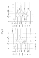
- Fig. 5 is a circuit diagram which shows a circuit structure of a latch circuit according to the second embodiment of the present invention.
- n type MOS transistors NMT1, NMT2 for processing a high voltage
- a p type MOS transistor PMT3 of the latch circuit shown in Fig. 1 are respectively replaced with double gate transistors, which improves source drain resistance. That is, in the present embodiment, the n type MOS transistor NMT1 which comprises the latch circuit shown in Fig. 1 is replaced with an n type MOS transistor NMT1 and an n type MOS transistor NMT11.
- the n type MOS transistor NMT2 which comprises the latch circuit in Fig.
- the latch circuit shown in Fig. 5 is that in which each of the transistors NMT1 and NMT2 shown in Fig. 1 are respectively replaced with a combination of two transistors which are input with the same gate voltage, that is, double gate transistors.
- the latch circuit of the present embodiment includes a p type MOS transistor PMT3 and a p type MOS transistor PMT31 which replaces the p type MOS transistor PMT3 of the latch circuit shown in Fig. 1 . That is, the latch circuit of the present embodiment is that in which the transistor PMT3 shown in Fig. 1 is replaced with a combination of two transistors supplied with the same voltage, that is, double gate transistors. In this way, by adopting a double gate transistor structure, the latch circuit of the second embodiment has increased effective source drain resistance to process high voltage.
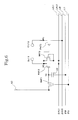
- Fig. 6 is a circuit diagram which shows a circuit structure of a latch circuit according to a third embodiment of the present invention.
- the latch circuit of the third embodiment is different to the latch circuit of the first embodiment shown in the Fig. 1 in the points that a diode-connected n type MOS transistor NMT3 is connected between a source and drain of the n type MOS transistor NMT2, and that a fixed voltage VL is supplied to the capacitance control line (LW).
- the n type MOS transistors (NMT1, NMT2, NMT3) and the p type MOS transistor PMT3 are MOS transistors having a semiconductor layer formed from polycrystalline silicon.
- Fig. 7 is a timing chart which shows variation in accordance with time elapse of a scanning pulse ( ⁇ G), a latch control signal ( ⁇ AC1, ( ⁇ AC2) and voltage of each node (N1, N2, N3) of the latch circuit shown in Fig. 6 .
- a voltage (data) on a signal line (LD) is an L level voltage
- the voltage of the node N1 is an H level voltage VDH
- that of the node N2 is an L Level voltage VL
- that of the node N3 is an H level voltage VH3, before a time t1.
- a scanning pulse ( ⁇ G) that is, a signal reading pulse (gate pulse)
- gate pulse a scanning line
- VH1 a H level voltage
- the n type MOS transistor (input transistor NMT1) is turned ON and the voltage of the node N1 becomes a voltage (data, here, a voltage VL) on the signal line (LD).
- the voltage of the first latch control signal ( ⁇ AC1) on the first latch control line (LAC1) becomes a voltage VL2 which is an intermediate voltage level, VL2 is set so that that the formula (4) below is satisfied, and the n MOS transistor NMT2 is maintained in an OFF state regardless of whether the voltage of the node N1 is a H level voltage VDH or a L level voltage VL.
- VL ⁇ 2 ⁇ VHD + Vth Vth is a threshold voltage of the transistor NMT ⁇ 2
- a second latch control signal ( ⁇ AC2) on a second latch control line (LAC2) changes from an H level voltage VH3 to an L level voltage VL at a time t2.
- whether the p type MOS transistor PMT3 is ON or OFF is determined by the voltage of the node N2.
- the node N2 is an L level voltage VL at a time t2
- the p type MOS transistor PMT3 is in an ON state and the voltage of the node N3 and the second latch control signal ( ⁇ AC2) become an L level voltage VL3.
- the first latch control signal ( ⁇ AC1) on the first latch control line (LAC1) changes from an intermediate voltage level voltage VL2 to an H level voltage VH3 at a time t3.
- VH4 is generally a voltage shown in the following formula: VH ⁇ 4 ⁇ VH ⁇ 22 - Vth
- the first latch control signal ( ⁇ AC1) on the first latch control line (LAC1) changes from an H level voltage VH3 to an L level voltage VL at a time t4.
- the n type MOS transistor NMT2 is maintained in an OFF state, the node N2 is maintained at an H level voltage VH4.
- the first latch control signal ( ⁇ AC1) on the first latch control line (LAC1) changes from an L level voltage VL to an intermediate voltage level voltage VL2 at a time t5.
- the second control latch signal ( ⁇ AC2) on the second latch control line (LAC2) changes from an L level voltage VL to an H level voltage VH3 at a time t6.
- a gate voltage of the p type MOS transistor PMT3 is a voltage of the node N2 and the voltage of the node N2 is an H level voltage VH4 at a time t6, the p type MOS transistor PMT3 is in an OFF state. Therefore, the node N3 is maintained at an L level voltage VL3.
- a voltage (data) on a signal line (LD) is an H level voltage VDH is explained.
- the voltage of the node N1 is an L level voltage VL
- that of the node N2 is an H level voltage VH4
- that of the node N3 is an L level voltage VL3.
- a scanning pulse ( ⁇ G) that is, a signal reading pulse (gate pulse)
- gate pulse a signal reading pulse
- the input transistor NMT1 is turned ON and the voltage of the node N1 becomes a voltage (data, here, a voltage VDH) on the signal line (LD).
- the voltage of the first latch control signal ( ⁇ AC1) on the first latch control line (LAC1) becomes a voltage VL2 which is an intermediate voltage level, and as described above, the n type MOS transistor NMT2 is maintained in an OFF state regardless of whether the voltage of the node N1 is a H level voltage VDH or a L level voltage VL, so that there is no variation in the output (latch state).
- the second latch control signal ( ⁇ AC2) on the second latch control line (LAC2) becomes an L level voltage VL at a time t22.
- the first latch control signal ( ⁇ AC1) on the first latch control line (LAC1) changes from an intermediate voltage level voltage VL2 to an H level voltage VH3 at a time t23.
- the diode connected n type MOS transistor NMT3 is in a conducting state, the voltage of the node N2 rises.
- the voltage of the node N2 is already an H level voltage VH4, the voltage of the node N2 does not change.
- the p type MOS transistor PMT3 is maintained in an OFF state.
- the n type MOS transistor NMT2 becomes an ON state and the voltage of the node N2 becomes a L level voltage VL. Together with this, the p type MOS transistor PMT3 becomes an ON state.
- the first control latch signal ( ⁇ AC1) on the first latch control line (LAC1) changes from an L level voltage VL to an intermediate voltage level voltage VL2 at a time t25.
- the n type MOS transistor NMT2 is maintained in an OFF state regardless of a programming voltage (VDH, VL) from the signal line (LD) to the node N1.
- VDH, VL programming voltage
- a gate voltage of the p type MOS transistor PMT3 is a voltage of the node N2 and the voltage of the node N2 is a L level voltage VL at a time t25, the p type MOS transistor PMT3 is maintained in an ON state.
- the second latch control signal ( ⁇ AC2) on the second latch control line (LAC2) changes from an L level voltage VL to an H level voltage VH3 at a time t26.
- the voltage of the node N3 rises to an H level voltage VH together with a rise in the second latch control signal ( ⁇ AC2).
- a signal voltage a voltage corresponding to "1" data
- a differential output state between the output terminal (OUT1) and the output terminal (OUT2) is latched.
- the shutter control signal ( ⁇ S) on the movable shutter control line (LSS) is generally a GND voltage (or a voltage VDD)
- the other end of the storage capacitance (CD) may also be connected to the movable shutter control line (LSS).
- Fig. 8 is a circuit diagram which shows a circuit structure of a latch circuit according to the fourth embodiment of the present invention.
- n type MOS transistors NMT1, NMT2, NMT3 for processing a high voltage
- a p type MOS transistor PMT3 of the latch circuit shown in Fig. 6 are respectively replaced with a double gate transistors, which improves source drain resistance.
- the n type MOS transistor NMT1 shown in Fig. 6 is replaced with an n type MOS transistor NMT1 and an n type MOS transistor NMT11, which means that the transistor NMT1 shown in Fig. 6 is replaced with a combination of two transistors which are input with the same gate voltage, that is, double gate transistors.
- the latch circuit of the fourth embodiment includes a structure in which the n type MOS transistor NMT2 shown in Fig. 6 is replaced with an n type MOS transistor NMT2 and a an n type MOS transistor NMT21, which means that the transistor NMT2 is replaced with a combination of two transistors which are input with the same voltage, that is, double gate transistors.
- the latch circuit of the fourth embodiment includes a structure in which the n type MOS transistor NMT3 shown in Fig. 6 is replaced with an n type MOS transistor NMT3 and a an n type MOS transistor NMT31, which means that the transistor NMT3 is replaced with a combination of two transistors which are input with the same voltage, that is double gate transistors.
- the latch circuit of the fourth embodiment includes a structure in which the p type MOS transistor PMT3 shown in Fig. 6 is replaced with a p type MOS transistor PMT3 and a p type MOS transistor PMT31, which means that the transistor PMT3 shown in Fig. 6 is replaced with a combination of two transistors respectively supplied with the same voltage, that is, double gate transistors.
- the latch circuit of the fourth embodiment has increased effective source drain resistance to process high voltage
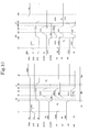
- Fig. 9 is a circuit diagram which shows a circuit structure of a latch circuit according to a fifth embodiment of the present invention.
- the latch circuit of the present embodiment is different to the latch circuit of the second embodiment in the points that an type MOS transistor NMT4 is connected between the drain of the n type MOS transistor NMT2 and the first latch control line (LAC1), that the gate of the n type MOS transistor NMT4 is connected to a third latch control line (LA) and that one end of the storage capacitance (CD) is connected to the first latch control line (LAC1).
- the n type MOS transistors (NMT1, NMT2, NMT3, NMT4) and the p type MOS transistor PMT3 are MOS transistors having a semiconductor layer formed from polycrystalline silicon.
- Fig. 10 is a timing chart which shows variation in accordance with time elapse of a scanning pulse ( ⁇ G), a latch control signal ( ⁇ AC1, ⁇ AC2, ⁇ A) and voltage of each node (N1, N2, N3, N4) of the latch circuit shown in Fig. 9 .
- a voltage (data) on a signal line (LD) is an L level voltage
- the voltage of the node N1 is an H level voltage VDH
- that of the node N2 is an L Level voltage VL
- that of the node N3 is an H level voltage VH3, before a time t1.
- Fig. 10 is a timing chart which shows variation in accordance with time elapse of a scanning pulse ( ⁇ G), a latch control signal ( ⁇ AC1, ⁇ AC2, ⁇ A) and voltage of each node (N1, N2, N3, N4) of the latch circuit shown in Fig. 9 .
- the voltage of the node N1 is an H level voltage VDH
- that of the node N2 is an
- a second latch control signal ( ⁇ AC2) on a second latch control line (LAC2) changes from an H level voltage VH3 to an L level voltage VL at a time t2.
- whether the p type MOS transistor PMT3 is ON or OFF is determined by the voltage of the node N2.
- the voltage of the node N2 is an L level voltage VL at a time t2
- the p type MOS transistor PMT3 is in an ON state and the voltage of the node N3 and the second latch control signal ( ⁇ AC2) become an L level voltage VL3.
- a voltage of the third latch control line (LA) changes from VL to VH21.
- the first latch control signal ( ⁇ AC1) on a first latch control line (LAC1) changes from an L level voltage VL to an H level voltage VH3 at a time t4. Because the diode connected n type MOS transistor NMT3 is in a conducting state, the voltage of the node N2 becomes an H level voltage VH4. Because one end of the storage capacitance (CD) is connected to the first latch control signal ( ⁇ AC1), the voltage of the node N1 becomes VH2.
- the first control signal ( ⁇ AC1) changes from an H level voltage VH3 to an L level voltage VL at a time t6. Together with this, the voltage of the node N1 which is capacitively coupled by the storage capacitance (CD) returns to a voltage VL. Therefore, because the n type MOS transistor NMT2 is in an OFF state, the node N2 is maintained at an H level voltage VH4. At this time, because the n type MOS transistor NMT4 is in an ON state, the node N4 returns to a voltage VL.
- the second latch control signal ( ⁇ AC2) changes from an L level voltage VL to an H level voltage VH3 at a time t8.
- the gate voltage of the p type MOS transistor PMT3 is a voltage of the node N2 and the voltage of the node N2 is a H level voltage VH4 at a time t8, the p type MOS transistor in in an OFF state, Therefore, the node N3 is maintained at a L level voltage VL3.
- the third latch control signal ( ⁇ A) changes to an L level voltage VL just after a time t8 and the n type MOS transistor NMT4 becomes in an OFF state. That is, during a period until the third latch control signal ( ⁇ A) changes to an H level voltage next, even if a voltage of the node N1 changes due to input of a signal, there is no change in the voltage of the node N2 and the node N3.
- the node N1 changes from an L level to an H level due to a signal being input
- the n type MOS transistor NMT2 changes from an OFF state to an ON state and the voltage of the node N4 changes from VL to VHD-Vth.
- a voltage (data) on the signal line (LD) is an H level voltage VDH is explained.
- the voltage of the node N1 is an L voltage VL
- that of the node N2 is an H level voltage VH4
- that of the node N3 is an L level voltage VL3.
- a scanning pulse ( ⁇ G) that is, a signal reading pulse (gate pulse)
- gate pulse a scanning line
- the input transistor (NMT1) is turned ON and the voltage of the node N1 becomes a voltage (data, here, a voltage VDH) on the signal line (LD).
- the n type MOS transistor NMT2 is in an ON state.
- the second latch control signal ( ⁇ AC2) on a second latch control line (LAC2) changes to an L level voltage VL.
- the third latch control signal ( ⁇ AC3) on the third latch control line (LA) changes from an L level voltage VL to an H level voltage VH21 at a time t23. In this way, the n type MOS transistor NMT4 is in an ON state.
- the voltage of the node N2 and the node N4 become a voltage VL.
- the p type MOS transistor PMT3 becomes in an ON state, whereas there is no change in the voltage of the output terminal (OUT2), because the voltage of the output terminal (OUT2) is already an L level voltage VL3.
- the first latch control signal ( ⁇ AC1) on a first latch control line (LAC1) changes to an H level voltage VH3 at a time t24.
- the voltage of the node N2 becomes an H level VH4 via the diode-connected n type MOS transistor NMT3.
- the voltage of the node N4 becomes a voltage VH5 and the voltage of the node N1 becomes VH3.
- the first latch control signal ( ⁇ AC1) on a first latch control line (LAC1) changes from an H level voltage VH3 to an L level voltage VL at a time t26. Together with this, the voltage of the node N1 returns to VHD. On the contrary, the voltages of the node N2 and the node N4 both become a L level voltage VL, because the n type MOS transistor NMT2 is in an ON state, the n type MOS transistor NMT4 is in an ON state, and the node N2 is connected to the first latch control line (LAC1) via the n type MOS transistor (NMT2, NMT4).
- the p type MOS transistor PMT3 becomes in an ON state at a time t27, because the gate voltage of the p type MOS transistor PMT3 is a voltage of the node N2 and the voltage of the node N2 is a L level voltage VL.
- the second latch control signal ( ⁇ AC2) on a second latch control line (LAC2) changes from an L level voltage VL to an H level voltage VH3 at a time t28.
- the p type MOS transistor PMT3 is in an ON state, the voltage of the node N3 rises to an H level voltage VH3 together with a rise of the second latch control signal ( ⁇ AC2).
- the following effects which are similar to the first embodiment can be obtained from the latch circuit of the present embodiment. Similar to the first and second embodiments, it is possible to apply the latch circuit of the present embodiment to the pixel circuit of the display (called a movable shutter type display) which electrically controls the position of shutters to display an image.
- the shutter control signal ( ⁇ S) on the movable shutter control line (LSS) is generally a GND voltage (or a voltage VDD)
- the other end of the storage capacitance (CD) may also be connected to the movable shutter control line (LSS).
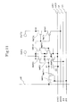
- Fig. 11 is a circuit diagram which shows a circuit structure of a latch circuit according to the sixth embodiment of the present invention.
- n type MOS transistors NMT1, NMT2, NMT3 for processing a high voltage
- a p type MOS transistor PMT3 of the latch circuit shown in Fig. 9 are respectively replaced with a double gate transistors, which improves source drain resistance.
- the n type MOS transistor NMT1 shown in Fig. 9 is replaced with an n type MOS transistor NMT1 and an n type MOS transistor NMT11, which means that the n type MOS transistor NMT1 shown in Fig. 9 is replaced with a combination of two transistors which are input with the same gate voltage, that is, double gate transistors.
- the n type MOS transistor NMT2 shown in Fig. 9 is replaced with an n type MOS transistor NMT2 and a an n type MOS transistor NMT21, which means that the n type MOS transistor NMT2 shown in Fig. 9 is replaced with a combination of two transistors which are input with the same voltage, that is, double gate transistors.
- the n type MOS transistor NMT3 shown in Fig. 9 is replaced with an n type MOS transistor NMT3 and an n type MOS transistor NMT31, which means that the n type MOS transistor NMT3 shown in Fig.
- the latch circuit of the sixth embodiment includes a structure in which the p type MOS transistor PMT3 shown in Fig. 9 is replaced with a p type MOS transistor PMT3 and a p type MOS transistor PMT31, which means that the transistor PMT3 shown in Fig. 9 is replaced with a combination of two transistors supplied with the same voltage, that is double gate transistors.
- the latch circuit of the sixth embodiment has increased effective source drain resistance and reduced high voltage.
- the n type MOS transistor NMT4 is not essentially applied with a VDH-Vth voltage or more, the transistor remains as a single gate transistor.
- the n type MOS transistor NMT4 may be replaced provided with double gate transistors.
- n type polycrystalline silicon thin film transistors are used for the first transistor NMT1, the third transistor NMT2, the fourth transistor NMT3 and the fifth transistor NMT4 and a p type polycrystalline silicon thin film transistor is used for the second transistor PMT3.
- a p type polycrystalline silicon thin film transistor for the first transistor NMT1, the third transistor NMT2, the fourth transistor NMT3 and the fifth transistor NMT4.
- an n type polycrystalline silicon thin film transistor for the second transistor PMT3.
Landscapes
- Engineering & Computer Science (AREA)
- Physics & Mathematics (AREA)
- Computer Hardware Design (AREA)
- General Physics & Mathematics (AREA)
- Theoretical Computer Science (AREA)
- Nonlinear Science (AREA)
- Control Of Indicators Other Than Cathode Ray Tubes (AREA)
- Mechanical Light Control Or Optical Switches (AREA)
- Logic Circuits (AREA)
- Liquid Crystal Display Device Control (AREA)
Applications Claiming Priority (1)
| Application Number | Priority Date | Filing Date | Title |
|---|---|---|---|
| JP2011227851A JP5856799B2 (ja) | 2011-10-17 | 2011-10-17 | ラッチ回路および表示装置 |
Publications (2)
| Publication Number | Publication Date |
|---|---|
| EP2584700A2 true EP2584700A2 (de) | 2013-04-24 |
| EP2584700A3 EP2584700A3 (de) | 2014-06-04 |
Family
ID=47022580
Family Applications (1)
| Application Number | Title | Priority Date | Filing Date |
|---|---|---|---|
| EP12188809.3A Withdrawn EP2584700A3 (de) | 2011-10-17 | 2012-10-17 | Sperrschaltung und Anzeigevorrichtung |
Country Status (6)
| Country | Link |
|---|---|
| US (2) | US9099997B2 (de) |
| EP (1) | EP2584700A3 (de) |
| JP (1) | JP5856799B2 (de) |
| KR (1) | KR101489744B1 (de) |
| CN (1) | CN103051315A (de) |
| TW (1) | TWI520487B (de) |
Families Citing this family (6)
| Publication number | Priority date | Publication date | Assignee | Title |
|---|---|---|---|---|
| CN109087680B (zh) * | 2018-08-31 | 2023-10-20 | 南京观海微电子有限公司 | 用于amoled平板子像素的一位存储器电路 |
| CN109920371B (zh) * | 2019-04-26 | 2021-01-29 | 京东方科技集团股份有限公司 | 像素电路及其驱动方法、显示装置 |
| CN110060646B (zh) * | 2019-05-08 | 2021-08-03 | 京东方科技集团股份有限公司 | 数据锁存电路、像素电路、阵列基板及液晶显示面板 |
| CN111477163B (zh) * | 2020-04-21 | 2021-09-28 | 京东方科技集团股份有限公司 | 像素驱动电路及其驱动方法、显示面板 |
| CN114255691B (zh) * | 2020-09-24 | 2023-06-09 | 京东方科技集团股份有限公司 | 一种像素电路及其驱动方法、以及显示装置 |
| CN113707077B (zh) * | 2021-08-25 | 2023-01-20 | 京东方科技集团股份有限公司 | 一种像素驱动电路及其驱动方法、显示基板 |
Citations (1)
| Publication number | Priority date | Publication date | Assignee | Title |
|---|---|---|---|---|
| JP2008197668A (ja) | 2005-02-23 | 2008-08-28 | Pixtronix Inc | 表示方法および装置 |
Family Cites Families (14)
| Publication number | Priority date | Publication date | Assignee | Title |
|---|---|---|---|---|
| US5592411A (en) | 1995-11-02 | 1997-01-07 | Motorola, Inc. | Non-volatile register and method for accessing data therein |
| JP2000200072A (ja) | 1998-11-04 | 2000-07-18 | Matsushita Electric Ind Co Ltd | 動作回路及びその動作回路を用いた液晶表示パネルの内蔵駆動回路 |
| JP4091301B2 (ja) | 2001-12-28 | 2008-05-28 | 富士通株式会社 | 半導体集積回路および半導体メモリ |
| US7142030B2 (en) * | 2002-12-03 | 2006-11-28 | Semiconductor Energy Laboratory Co., Ltd. | Data latch circuit and electronic device |
| JP4296492B2 (ja) | 2003-12-01 | 2009-07-15 | ソニー株式会社 | ラッチ回路、シフトレジスタ回路、表示装置の駆動回路、表示装置 |
| KR20060003968A (ko) | 2004-07-05 | 2006-01-12 | 삼성전자주식회사 | 어레이 기판과 이를 갖는 표시 장치와, 이의 구동장치 및방법 |
| EP2116885B1 (de) | 2005-02-23 | 2014-07-23 | Pixtronix, Inc. | Anzeigeverfahren und -vorrichtung |
| US8482496B2 (en) | 2006-01-06 | 2013-07-09 | Pixtronix, Inc. | Circuits for controlling MEMS display apparatus on a transparent substrate |
| JP2007240698A (ja) | 2006-03-07 | 2007-09-20 | Oki Electric Ind Co Ltd | 電流駆動回路 |
| WO2008120275A1 (ja) | 2007-03-29 | 2008-10-09 | Fujitsu Limited | 移動通信装置 |
| BR112012019383A2 (pt) * | 2010-02-02 | 2017-09-12 | Pixtronix Inc | Circuitos para controlar aparelho de exibição |
| JP2012239046A (ja) * | 2011-05-12 | 2012-12-06 | Japan Display East Co Ltd | ラッチ回路およびラッチ回路を用いた表示装置 |
| US8902205B2 (en) * | 2011-06-01 | 2014-12-02 | Pixtronix, Inc. | Latching circuits for MEMS display devices |
| US9235047B2 (en) * | 2011-06-01 | 2016-01-12 | Pixtronix, Inc. | MEMS display pixel control circuits and methods |
-
2011
- 2011-10-17 JP JP2011227851A patent/JP5856799B2/ja not_active Expired - Fee Related
-
2012
- 2012-10-11 TW TW101137541A patent/TWI520487B/zh not_active IP Right Cessation
- 2012-10-15 US US13/651,785 patent/US9099997B2/en not_active Expired - Fee Related
- 2012-10-17 EP EP12188809.3A patent/EP2584700A3/de not_active Withdrawn
- 2012-10-17 CN CN2012103947358A patent/CN103051315A/zh active Pending
- 2012-10-17 KR KR20120115125A patent/KR101489744B1/ko not_active Expired - Fee Related
-
2015
- 2015-06-26 US US14/752,361 patent/US20150295568A1/en not_active Abandoned
Patent Citations (1)
| Publication number | Priority date | Publication date | Assignee | Title |
|---|---|---|---|---|
| JP2008197668A (ja) | 2005-02-23 | 2008-08-28 | Pixtronix Inc | 表示方法および装置 |
Also Published As
| Publication number | Publication date |
|---|---|
| US20130093649A1 (en) | 2013-04-18 |
| US9099997B2 (en) | 2015-08-04 |
| TW201325093A (zh) | 2013-06-16 |
| JP2013090086A (ja) | 2013-05-13 |
| CN103051315A (zh) | 2013-04-17 |
| KR101489744B1 (ko) | 2015-02-04 |
| TWI520487B (zh) | 2016-02-01 |
| JP5856799B2 (ja) | 2016-02-10 |
| US20150295568A1 (en) | 2015-10-15 |
| EP2584700A3 (de) | 2014-06-04 |
| KR20130041751A (ko) | 2013-04-25 |
Similar Documents
| Publication | Publication Date | Title |
|---|---|---|
| JP7001805B2 (ja) | シフトレジスタ及びその駆動方法、ゲート駆動回路と表示装置 | |
| JP5851594B2 (ja) | Mems表示デバイス用のラッチ回路 | |
| EP2838079B1 (de) | Schieberegistereinheit und ansteuerungsverfahren dafür, schieberegister und anzeigevorrichtung | |
| US9715940B2 (en) | Shift register | |
| US20180122289A1 (en) | Shift register, driving method, gate driving circuit and display device | |
| JP6914270B2 (ja) | シフトレジスタユニット及びその駆動方法、ゲート駆動回路 | |
| US9632527B2 (en) | Shift register | |
| US20170256204A1 (en) | Shift Register Unit, Organic Light-Emitting Display Panel And Driving Method | |
| KR102126455B1 (ko) | 버퍼 회로 및 버퍼 회로의 구동 방법 | |
| US10115348B2 (en) | Pixel circuit, driving method thereof and organic electroluminescent display panel | |
| EP2584700A2 (de) | Sperrschaltung und Anzeigevorrichtung | |
| KR101977579B1 (ko) | 디스플레이 패널 그리고 디스플레이 패널을 위한 구동 회로 | |
| KR101383865B1 (ko) | 래치회로 및 래치회로를 이용한 표시장치 | |
| KR20160043175A (ko) | 게이트 구동회로와 이를 이용한 표시장치 | |
| US10770003B2 (en) | Transfer circuit, shift register, gate driver, display panel, and flexible substrate | |
| KR20160107626A (ko) | 게이트 드라이버 |
Legal Events
| Date | Code | Title | Description |
|---|---|---|---|
| PUAI | Public reference made under article 153(3) epc to a published international application that has entered the european phase |
Free format text: ORIGINAL CODE: 0009012 |
|
| AK | Designated contracting states |
Kind code of ref document: A2 Designated state(s): AL AT BE BG CH CY CZ DE DK EE ES FI FR GB GR HR HU IE IS IT LI LT LU LV MC MK MT NL NO PL PT RO RS SE SI SK SM TR |
|
| AX | Request for extension of the european patent |
Extension state: BA ME |
|
| RAP1 | Party data changed (applicant data changed or rights of an application transferred) |
Owner name: JAPAN DISPLAY INC. |
|
| 17P | Request for examination filed |
Effective date: 20130705 |
|
| RAP1 | Party data changed (applicant data changed or rights of an application transferred) |
Owner name: PIXTRONIX, INC. |
|
| RIC1 | Information provided on ipc code assigned before grant |
Ipc: G09G 3/36 20060101AFI20140114BHEP Ipc: H03K 3/356 20060101ALI20140114BHEP |
|
| PUAL | Search report despatched |
Free format text: ORIGINAL CODE: 0009013 |
|
| AK | Designated contracting states |
Kind code of ref document: A3 Designated state(s): AL AT BE BG CH CY CZ DE DK EE ES FI FR GB GR HR HU IE IS IT LI LT LU LV MC MK MT NL NO PL PT RO RS SE SI SK SM TR |
|
| AX | Request for extension of the european patent |
Extension state: BA ME |
|
| RIC1 | Information provided on ipc code assigned before grant |
Ipc: H03K 3/356 20060101ALI20140429BHEP Ipc: G09G 3/36 20060101AFI20140429BHEP |
|
| RBV | Designated contracting states (corrected) |
Designated state(s): AL AT BE BG CH CY CZ DE DK EE ES FI FR GB GR HR HU IE IS IT LI LT LU LV MC MK MT NL NO PL PT RO RS SE SI SK SM TR |
|
| 17Q | First examination report despatched |
Effective date: 20160520 |
|
| RAP1 | Party data changed (applicant data changed or rights of an application transferred) |
Owner name: SNAPTRACK, INC. |
|
| STAA | Information on the status of an ep patent application or granted ep patent |
Free format text: STATUS: THE APPLICATION IS DEEMED TO BE WITHDRAWN |
|
| 18D | Application deemed to be withdrawn |
Effective date: 20161001 |