EP2582218B1 - Wärmeableitung über den Hinterrahmen einer Anzeigevorrichtung - Google Patents
Wärmeableitung über den Hinterrahmen einer Anzeigevorrichtung Download PDFInfo
- Publication number
- EP2582218B1 EP2582218B1 EP12188067.8A EP12188067A EP2582218B1 EP 2582218 B1 EP2582218 B1 EP 2582218B1 EP 12188067 A EP12188067 A EP 12188067A EP 2582218 B1 EP2582218 B1 EP 2582218B1
- Authority
- EP
- European Patent Office
- Prior art keywords
- rear housing
- heat radiation
- radiation member
- projecting portion
- display according
- Prior art date
- Legal status (The legal status is an assumption and is not a legal conclusion. Google has not performed a legal analysis and makes no representation as to the accuracy of the status listed.)
- Not-in-force
Links
Images




Classifications
-
- G—PHYSICS
- G02—OPTICS
- G02F—OPTICAL DEVICES OR ARRANGEMENTS FOR THE CONTROL OF LIGHT BY MODIFICATION OF THE OPTICAL PROPERTIES OF THE MEDIA OF THE ELEMENTS INVOLVED THEREIN; NON-LINEAR OPTICS; FREQUENCY-CHANGING OF LIGHT; OPTICAL LOGIC ELEMENTS; OPTICAL ANALOGUE/DIGITAL CONVERTERS
- G02F1/00—Devices or arrangements for the control of the intensity, colour, phase, polarisation or direction of light arriving from an independent light source, e.g. switching, gating or modulating; Non-linear optics
- G02F1/01—Devices or arrangements for the control of the intensity, colour, phase, polarisation or direction of light arriving from an independent light source, e.g. switching, gating or modulating; Non-linear optics for the control of the intensity, phase, polarisation or colour
- G02F1/13—Devices or arrangements for the control of the intensity, colour, phase, polarisation or direction of light arriving from an independent light source, e.g. switching, gating or modulating; Non-linear optics for the control of the intensity, phase, polarisation or colour based on liquid crystals, e.g. single liquid crystal display cells
- G02F1/133—Constructional arrangements; Operation of liquid crystal cells; Circuit arrangements
- G02F1/1333—Constructional arrangements; Manufacturing methods
- G02F1/1335—Structural association of cells with optical devices, e.g. polarisers or reflectors
- G02F1/1336—Illuminating devices
- G02F1/133615—Edge-illuminating devices, i.e. illuminating from the side
-
- G—PHYSICS
- G02—OPTICS
- G02B—OPTICAL ELEMENTS, SYSTEMS OR APPARATUS
- G02B6/00—Light guides; Structural details of arrangements comprising light guides and other optical elements, e.g. couplings
- G02B6/0001—Light guides; Structural details of arrangements comprising light guides and other optical elements, e.g. couplings specially adapted for lighting devices or systems
- G02B6/0011—Light guides; Structural details of arrangements comprising light guides and other optical elements, e.g. couplings specially adapted for lighting devices or systems the light guides being planar or of plate-like form
- G02B6/0081—Mechanical or electrical aspects of the light guide and light source in the lighting device peculiar to the adaptation to planar light guides, e.g. concerning packaging
- G02B6/0086—Positioning aspects
- G02B6/0088—Positioning aspects of the light guide or other optical sheets in the package
-
- G—PHYSICS
- G02—OPTICS
- G02B—OPTICAL ELEMENTS, SYSTEMS OR APPARATUS
- G02B6/00—Light guides; Structural details of arrangements comprising light guides and other optical elements, e.g. couplings
- G02B6/0001—Light guides; Structural details of arrangements comprising light guides and other optical elements, e.g. couplings specially adapted for lighting devices or systems
- G02B6/0011—Light guides; Structural details of arrangements comprising light guides and other optical elements, e.g. couplings specially adapted for lighting devices or systems the light guides being planar or of plate-like form
- G02B6/0066—Light guides; Structural details of arrangements comprising light guides and other optical elements, e.g. couplings specially adapted for lighting devices or systems the light guides being planar or of plate-like form characterised by the light source being coupled to the light guide
- G02B6/0068—Arrangements of plural sources, e.g. multi-colour light sources
-
- G—PHYSICS
- G02—OPTICS
- G02B—OPTICAL ELEMENTS, SYSTEMS OR APPARATUS
- G02B6/00—Light guides; Structural details of arrangements comprising light guides and other optical elements, e.g. couplings
- G02B6/0001—Light guides; Structural details of arrangements comprising light guides and other optical elements, e.g. couplings specially adapted for lighting devices or systems
- G02B6/0011—Light guides; Structural details of arrangements comprising light guides and other optical elements, e.g. couplings specially adapted for lighting devices or systems the light guides being planar or of plate-like form
- G02B6/0066—Light guides; Structural details of arrangements comprising light guides and other optical elements, e.g. couplings specially adapted for lighting devices or systems the light guides being planar or of plate-like form characterised by the light source being coupled to the light guide
- G02B6/0073—Light emitting diode [LED]
-
- G—PHYSICS
- G02—OPTICS
- G02B—OPTICAL ELEMENTS, SYSTEMS OR APPARATUS
- G02B6/00—Light guides; Structural details of arrangements comprising light guides and other optical elements, e.g. couplings
- G02B6/0001—Light guides; Structural details of arrangements comprising light guides and other optical elements, e.g. couplings specially adapted for lighting devices or systems
- G02B6/0011—Light guides; Structural details of arrangements comprising light guides and other optical elements, e.g. couplings specially adapted for lighting devices or systems the light guides being planar or of plate-like form
- G02B6/0081—Mechanical or electrical aspects of the light guide and light source in the lighting device peculiar to the adaptation to planar light guides, e.g. concerning packaging
- G02B6/0085—Means for removing heat created by the light source from the package
-
- G—PHYSICS
- G06—COMPUTING OR CALCULATING; COUNTING
- G06F—ELECTRIC DIGITAL DATA PROCESSING
- G06F1/00—Details not covered by groups G06F3/00 - G06F13/00 and G06F21/00
- G06F1/16—Constructional details or arrangements
- G06F1/20—Cooling means
-
- H—ELECTRICITY
- H05—ELECTRIC TECHNIQUES NOT OTHERWISE PROVIDED FOR
- H05K—PRINTED CIRCUITS; CASINGS OR CONSTRUCTIONAL DETAILS OF ELECTRIC APPARATUS; MANUFACTURE OF ASSEMBLAGES OF ELECTRICAL COMPONENTS
- H05K1/00—Printed circuits
- H05K1/02—Details
- H05K1/0201—Thermal arrangements, e.g. for cooling, heating or preventing overheating
- H05K1/0203—Cooling of mounted components
- H05K1/0209—External configuration of printed circuit board adapted for heat dissipation, e.g. lay-out of conductors, coatings
-
- H—ELECTRICITY
- H05—ELECTRIC TECHNIQUES NOT OTHERWISE PROVIDED FOR
- H05K—PRINTED CIRCUITS; CASINGS OR CONSTRUCTIONAL DETAILS OF ELECTRIC APPARATUS; MANUFACTURE OF ASSEMBLAGES OF ELECTRICAL COMPONENTS
- H05K7/00—Constructional details common to different types of electric apparatus
- H05K7/20—Modifications to facilitate cooling, ventilating, or heating
- H05K7/20954—Modifications to facilitate cooling, ventilating, or heating for display panels
- H05K7/20963—Heat transfer by conduction from internal heat source to heat radiating structure
-
- G—PHYSICS
- G02—OPTICS
- G02F—OPTICAL DEVICES OR ARRANGEMENTS FOR THE CONTROL OF LIGHT BY MODIFICATION OF THE OPTICAL PROPERTIES OF THE MEDIA OF THE ELEMENTS INVOLVED THEREIN; NON-LINEAR OPTICS; FREQUENCY-CHANGING OF LIGHT; OPTICAL LOGIC ELEMENTS; OPTICAL ANALOGUE/DIGITAL CONVERTERS
- G02F1/00—Devices or arrangements for the control of the intensity, colour, phase, polarisation or direction of light arriving from an independent light source, e.g. switching, gating or modulating; Non-linear optics
- G02F1/01—Devices or arrangements for the control of the intensity, colour, phase, polarisation or direction of light arriving from an independent light source, e.g. switching, gating or modulating; Non-linear optics for the control of the intensity, phase, polarisation or colour
- G02F1/13—Devices or arrangements for the control of the intensity, colour, phase, polarisation or direction of light arriving from an independent light source, e.g. switching, gating or modulating; Non-linear optics for the control of the intensity, phase, polarisation or colour based on liquid crystals, e.g. single liquid crystal display cells
- G02F1/133—Constructional arrangements; Operation of liquid crystal cells; Circuit arrangements
- G02F1/1333—Constructional arrangements; Manufacturing methods
- G02F1/133308—Support structures for LCD panels, e.g. frames or bezels
- G02F1/133314—Back frames
-
- G—PHYSICS
- G02—OPTICS
- G02F—OPTICAL DEVICES OR ARRANGEMENTS FOR THE CONTROL OF LIGHT BY MODIFICATION OF THE OPTICAL PROPERTIES OF THE MEDIA OF THE ELEMENTS INVOLVED THEREIN; NON-LINEAR OPTICS; FREQUENCY-CHANGING OF LIGHT; OPTICAL LOGIC ELEMENTS; OPTICAL ANALOGUE/DIGITAL CONVERTERS
- G02F1/00—Devices or arrangements for the control of the intensity, colour, phase, polarisation or direction of light arriving from an independent light source, e.g. switching, gating or modulating; Non-linear optics
- G02F1/01—Devices or arrangements for the control of the intensity, colour, phase, polarisation or direction of light arriving from an independent light source, e.g. switching, gating or modulating; Non-linear optics for the control of the intensity, phase, polarisation or colour
- G02F1/13—Devices or arrangements for the control of the intensity, colour, phase, polarisation or direction of light arriving from an independent light source, e.g. switching, gating or modulating; Non-linear optics for the control of the intensity, phase, polarisation or colour based on liquid crystals, e.g. single liquid crystal display cells
- G02F1/133—Constructional arrangements; Operation of liquid crystal cells; Circuit arrangements
- G02F1/1333—Constructional arrangements; Manufacturing methods
- G02F1/133308—Support structures for LCD panels, e.g. frames or bezels
- G02F1/133317—Intermediate frames, e.g. between backlight housing and front frame
-
- G—PHYSICS
- G02—OPTICS
- G02F—OPTICAL DEVICES OR ARRANGEMENTS FOR THE CONTROL OF LIGHT BY MODIFICATION OF THE OPTICAL PROPERTIES OF THE MEDIA OF THE ELEMENTS INVOLVED THEREIN; NON-LINEAR OPTICS; FREQUENCY-CHANGING OF LIGHT; OPTICAL LOGIC ELEMENTS; OPTICAL ANALOGUE/DIGITAL CONVERTERS
- G02F1/00—Devices or arrangements for the control of the intensity, colour, phase, polarisation or direction of light arriving from an independent light source, e.g. switching, gating or modulating; Non-linear optics
- G02F1/01—Devices or arrangements for the control of the intensity, colour, phase, polarisation or direction of light arriving from an independent light source, e.g. switching, gating or modulating; Non-linear optics for the control of the intensity, phase, polarisation or colour
- G02F1/13—Devices or arrangements for the control of the intensity, colour, phase, polarisation or direction of light arriving from an independent light source, e.g. switching, gating or modulating; Non-linear optics for the control of the intensity, phase, polarisation or colour based on liquid crystals, e.g. single liquid crystal display cells
- G02F1/133—Constructional arrangements; Operation of liquid crystal cells; Circuit arrangements
- G02F1/1333—Constructional arrangements; Manufacturing methods
- G02F1/133308—Support structures for LCD panels, e.g. frames or bezels
- G02F1/133328—Segmented frames
-
- G—PHYSICS
- G02—OPTICS
- G02F—OPTICAL DEVICES OR ARRANGEMENTS FOR THE CONTROL OF LIGHT BY MODIFICATION OF THE OPTICAL PROPERTIES OF THE MEDIA OF THE ELEMENTS INVOLVED THEREIN; NON-LINEAR OPTICS; FREQUENCY-CHANGING OF LIGHT; OPTICAL LOGIC ELEMENTS; OPTICAL ANALOGUE/DIGITAL CONVERTERS
- G02F1/00—Devices or arrangements for the control of the intensity, colour, phase, polarisation or direction of light arriving from an independent light source, e.g. switching, gating or modulating; Non-linear optics
- G02F1/01—Devices or arrangements for the control of the intensity, colour, phase, polarisation or direction of light arriving from an independent light source, e.g. switching, gating or modulating; Non-linear optics for the control of the intensity, phase, polarisation or colour
- G02F1/13—Devices or arrangements for the control of the intensity, colour, phase, polarisation or direction of light arriving from an independent light source, e.g. switching, gating or modulating; Non-linear optics for the control of the intensity, phase, polarisation or colour based on liquid crystals, e.g. single liquid crystal display cells
- G02F1/133—Constructional arrangements; Operation of liquid crystal cells; Circuit arrangements
- G02F1/1333—Constructional arrangements; Manufacturing methods
- G02F1/1335—Structural association of cells with optical devices, e.g. polarisers or reflectors
- G02F1/1336—Illuminating devices
- G02F1/133628—Illuminating devices with cooling means
-
- H—ELECTRICITY
- H05—ELECTRIC TECHNIQUES NOT OTHERWISE PROVIDED FOR
- H05K—PRINTED CIRCUITS; CASINGS OR CONSTRUCTIONAL DETAILS OF ELECTRIC APPARATUS; MANUFACTURE OF ASSEMBLAGES OF ELECTRICAL COMPONENTS
- H05K2201/00—Indexing scheme relating to printed circuits covered by H05K1/00
- H05K2201/01—Dielectrics
- H05K2201/0137—Materials
- H05K2201/0162—Silicon containing polymer, e.g. silicone
-
- H—ELECTRICITY
- H05—ELECTRIC TECHNIQUES NOT OTHERWISE PROVIDED FOR
- H05K—PRINTED CIRCUITS; CASINGS OR CONSTRUCTIONAL DETAILS OF ELECTRIC APPARATUS; MANUFACTURE OF ASSEMBLAGES OF ELECTRICAL COMPONENTS
- H05K2201/00—Indexing scheme relating to printed circuits covered by H05K1/00
- H05K2201/09—Shape and layout
- H05K2201/09818—Shape or layout details not covered by a single group of H05K2201/09009 - H05K2201/09809
- H05K2201/09909—Special local insulating pattern, e.g. as dam around component
Definitions
- the present invention relates to a display, and more particularly, it relates to a display each including a heat radiation member for radiating heat generated by a light source portion.
- a display including a heat radiation member for radiating heat generated by a light source portion is known in general, as disclosed in Japanese Patent Laying-Open No. 2008-130413 , for example.
- the aforementioned Japanese Patent Laying-Open No. 2008-130413 discloses a liquid crystal display including a liquid crystal panel, a light guide arranged at the back of the liquid crystal panel, an LED (light source portion) arranged on a side portion of the light guide, a reflection sheet arranged at the back of the light guide, a back case (heat radiation member) arranged at the back of the LED and the reflection sheet and a heat sink arranged at the back of the back case for functioning as a rear housing.
- the back case is arranged to cover the whole of a region where the LED and the reflection sheet are arranged in a state in contact with the LED and the reflection sheet.
- the heat sink (rear housing) at the back of the back case is arranged to cover the whole of a region where the back case is arranged.
- the back case covering the LED and the reflection sheet is arranged on a region substantially equal to that where the heat sink (rear housing) is arranged as viewed from behind in the aforementioned liquid crystal display.
- the aforementioned liquid crystal display is so formed that the heat sink (rear housing) radiates heat generated by the LED through the back case in a normal use state.
- the back case (heat radiation member) radiating the heat generated by the LED is arranged on the region substantially equal to that where the heat sink (rear housing) is arranged as viewed from behind, and hence the area of the region where the back case is arranged is disadvantageously increased.
- KR 101 054 767 discloses subject-matter according to the preamble of claim 1.
- the present invention has been proposed in order to solve the aforementioned problem, and an object of the present invention is to provide a display capable of reducing the area of a region where a heat radiation member is arranged while excellently radiating heat generated by a light source portion.
- a display according to the present invention includes the features of appended claim 1.
- the first heat radiation member is arranged in a region of the rear housing exposed outward from the cover member as viewed from the side of the rear surface, whereby heat generated by the light source portion can be excellently radiated from the outwardly exposed region of the rear housing through the first heat radiation member, dissimilarly to a case where the first heat radiation member is arranged on a region corresponding to a region of the rear housing covered with the cover member as viewed from the side of the rear surface. Further, the area of the region where the first heat radiation member is arranged can be reduced dissimilarly to a case where the first heat radiation member is arranged on a region substantially equal to a region where the rear housing is arranged, for example. Thus, the area of the region where the first heat radiation member is arranged can be reduced while excellently radiating the heat generated by the light source portion.
- the light source portion is preferably mounted on the first heat radiation member, and the first heat radiation member mounted with the light source portion is preferably arranged in the region of the rear housing exposed outward from the cover member as viewed from the side of the rear surface of the rear housing. According to this structure, the distance between the light source portion mounted on the first heat radiation member and the outwardly exposed region of the rear housing can be relatively reduced, whereby the heat generated by the light source portion can be quickly radiated from the outwardly exposed region of the rear housing through the first heat radiation member.
- the first projecting portion can easily and more effectively radiate the heat.
- both of the outer surface of the first projecting portion of the first heat radiation member and a portion of the inner surface of the rear housing corresponding to the outer surface of the first projecting portion are preferably in the form of planar surfaces. According to this structure, the surface of the first projecting portion of the first heat radiation member and the portion of the inner surface of the rear housing corresponding to the surface of the first projecting portion can be easily brought into surface contact with each other.
- the aforementioned display can also include the features of appended claim 5.
- the region where the surface of the first projecting portion of the first heat radiation member and the inner surface of the rear housing are in surface contact with each other is arranged to extend along one side so that the heat radiation area can be increased, whereby heat radiation can be more effectively performed.
- the aforementioned display can also include the features of appended claim 4.
- the surface of the second projecting portion of the first heat radiation member and the surface of the recess portion of the rear housing closer to the first heat radiation member can be pressure-welded to each other in the state in surface contact with each other, whereby heat can be rendered more easily conductible, and heat radiation can be more effectively performed.
- both of the surface of the second projecting portion of the first heat radiation member and the surface of the recess portion of the rear housing closer to the first heat radiation member are preferably in the form of planar surfaces. According to this structure, the surface of the second projecting portion of the first heat radiation member and the surface of the recess portion of the rear housing closer to the first heat radiation member can be easily brought into surface contact with each other.
- the aforementioned display can include the features of appended claim 6.
- the surface of the first projecting portion of the first heat radiation member and the portion of the inner surface of the rear housing corresponding to the surface of the first projecting portion come into surface contact with each other on a vertical position higher than that of the second projecting portion, whereby the surface of the first projecting portion of the first heat radiation member and the portion of the inner surface of the rear housing corresponding to the surface of the first projecting portion can be easily brought into surface contact with each other while pressure-welding the surface of the second projecting portion and the surface of the recess portion of the rear housing closer to the first heat radiation member to each other in the surface contact state.
- the light source portion preferably includes a backlight LED source. According to this structure, heat generated by the backlight LED source can be excellently radiated from the outwardly exposed region of the rear housing through the first heat radiation member.
- the aforementioned display according to the invention preferably further includes the features of appended claim 8. According to this structure, the heat generated by the heating element can be easily radiated from the outwardly exposed region of the rear housing through the second heat radiation member also when the circuit board mounted with the heating element is covered with the cover member.
- the display is formed according to the features of appended claim 9.
- the thickness of the second heat radiation member can be reduced by the height of the third projecting portion formed on the rear housing while the heat generated by the heating element is indirectly radiated from the outwardly exposed region of the rear housing through the second heat radiation member and the third projecting portion of the rear housing, whereby the heat generated by the heating element can be easily radiated.
- a surface of the third projecting portion closer to the circuit board is preferably in the form of a planar surface.
- the second heat radiation member can be easily fixed by arranging the second heat radiation member in a clearance between the surface of the third projecting portion, provided in the form of a planar surface, closer to the circuit board and the circuit board to be held therebetween.
- the rear housing preferably has a board mounting portion protruding toward the circuit board so that the circuit board is fixed thereto, and a protrusion height of the board mounting portion with respect to the rear surface of the rear housing is preferably larger than a protrusion height of the third projecting portion with respect to the rear surface of the rear housing.
- the circuit board is fixed on a vertical position higher than that of the third projecting portion, whereby the second heat radiation member can be easily arranged in the clearance between the surface of the third projecting portion closer to the circuit board and the circuit board to be held therebetween.
- the first heat radiation member and the rear housing are preferably made of metal. According to this structure, the heat generated by the light source portion or the heating element can be rendered easily conductible, whereby heat radiation efficiency can be improved.
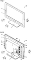
- the structure of a liquid crystal television set 100 according to the embodiment of the present invention is described with reference to Figs. 1 to 12 .
- the liquid crystal television set 100 is an example of the "display" in the present invention.
- the liquid crystal television set 100 has a rectangular shape, and includes a frame-shaped front housing 1, a liquid crystal cell 2 stored in the front housing 1 and a stand member 3 supporting the overall liquid crystal television set 100, as shown in Figs. 1 and 2 . Both of the front housing 1 and the stand member 3 are made of resin.
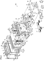
- a metal rear housing 4 made of sheet metal (SECC: electrolytic zinc-plated steel) is arranged on the side (along arrow Y2) of the rear surface of the front housing 1, as shown in Figs. 2 and 3 .
- the rear housing 4 has a rectangular shape and is formed to be smaller than the front housing 1 as viewed from behind, as shown in Fig. 3 .
- a cover member 5 made of resin is mounted on the rear surface of the metal rear housing 4.
- the cover member 5 has a rectangular shape and is formed to be smaller than the front housing 1 and the rear housing 4 as viewed from behind.
- the cover member 5 covers the rear surface of the rear housing 4 so that a portion around an outer peripheral surface of the rear surface (back surface) of the rear housing 4 is exposed in an inverted U-shaped manner as viewed from behind.
- An outwardly exposed region 401 of the rear housing 4 is formed to function as a heat radiation portion radiating heat generated by an LED source 6a and a heating element 81 (see Fig. 4 ) of a circuit board 8.
- a circuit board 7 having a function of supplying power to the overall liquid crystal television set 100 and the circuit board 8 performing signal processing are mounted on a region 402 of the rear surface of the rear housing 4 mounted with the cover member 5, to align with each other at a prescribed interval in a direction X.
- the heating element 81 such as an IC generating heat in a normal use state is mounted on the circuit board 8.
- a thermal pad mounting portion 41 protruding toward the inner surface of the cover member 5 is formed on a region of the rear surface (along arrow Y2) of the rear housing 4 corresponding to the heating element 81 of the circuit board 8.
- the thermal pad mounting portion 41 is the "third projecting portion” in the present embodiment.
- a thermal pad 82 for radiating heat generated by the heating element 81 toward the side of the rear housing 4 is arranged between the thermal pad mounting portion 41 of the rear housing 4 and the heating element 81 of the circuit board 8 to be held therebetween.
- the thermal pad 82 is the "second heat radiation member" in the present embodiment.
- the thermal pad 82 is made of a mixed material of silicone polymer and ceramic or the like.
- a reflection sheet holder 9a made of sheet metal (SECC), another reflection sheet holder 9b, still another reflection sheet holder 9c and a heat sink 10 made of sheet metal (SECC) are arranged in front of the rear housing 4 (along arrow Y1).
- a reflection sheet 11, a light guide 12, a light diffusion sheet 13, a lens sheet 14, a frame-shaped resin frame 15, the liquid crystal cell 2 mounted with a liquid crystal cell driving board 2a driving the liquid crystal cell 2 and four bezels 16 are arranged in front of the reflection sheet holders 9a, 9b and 9c and the heat sink 10 (along arrow Y1).
- the heat sink 10 is the "first heat radiation member" in the present embodiment.
- the backlight LED source 6a constituted of a plurality of LEDs is arranged on a side portion of the light guide 12, as shown in Figs. 8 and 9 .
- the LED source 6a generates heat in the normal use state of the liquid crystal television set 100.
- the LED source 6a is mounted on a surface of an LED board 6b along arrow X1.
- Another surface (opposite to the surface mounted with the LED source 6a) of the LED board 6b along arrow X2 is mounted on a surface of the heat sink 10 along arrow X1 through a heat radiation tape (sheet) 6c.
- the "light source portion" in the present invention is so constituted as to include the LED source 6a, the LED board 6b and the heat radiation tape 6c.
- screw receiving holes 10a for mounting the reflection sheet holders 9a and 9b are formed in the heat sink 10.
- Heat sink mounting threaded holes 91a and 91b for mounting the heat sink 10 are formed on left ends of the reflection sheet holders 9a and 9b respectively.
- Screws 30 are mounted on the heat sink mounting threaded holes 91a and 91b of the reflection sheet holders 9a and 9b through the screw receiving holes 10a of the heat sink 10 respectively, thereby fixing the heat sink 10 and the reflection sheet holders 9a and 9b to each other.
- Screw receiving holes 10b for mounting the corresponding bezels 16 are formed on upper and lower end portions of the heat sink 10 respectively.
- bezel mounting threaded holes 93a for mounting the corresponding bezel 16 are formed on right and left ends of the reflection sheet holder 9a respectively
- bezel mounting threaded holes 93b for mounting the corresponding bezel 16 are formed on right and left ends of the reflection sheet holder 9b respectively.
- screw receiving holes 16a for mounting screws 30 are formed in the bezels 16.
- the screws 30 are mounted on the bezel mounting threaded holes 93a and 93b formed on the left ends of the reflection sheet holders 9a and 9b respectively through the screw receiving holes 16a of the bezels 16 and the screw receiving holes 10b of the heat sink 10, thereby fixing the bezels 16, the heat sink 10 and the reflection sheet holders 9a and 9b to each other.
- a plurality of board mounting portions 42 for mounting the respective ones of the circuit boards 7 and 8 are formed on the rear surface (bottom surface) of the rear housing 4.
- the plurality of board mounting portions 42 are formed to protrude toward the cover member 5.
- the plurality of board mounting portions 42 are provided with board mounting threaded holes 4a.
- the height (protrusion height with respect to the rear surface of the rear housing 4) H1 of the board mounting portions 42 of the rear housing 4 is larger than the height (protrusion height with respect to the rear surface of the rear housing 4) H2 of the thermal pad mounting portion 41 of the rear housing 4. All of surfaces of the board mounting portions 42 closer to the circuit board 8 (along arrow Y2) and a surface of the thermal pad mounting portion 41 closer to the circuit board 8 are in the form of planar surfaces.
- a plurality of screw receiving holes 7a for receiving a plurality of screws 30 are formed on outer edge portions of the circuit board 7.
- the plurality of screws 30 are mounted on the plurality of board mounting threaded holes 4a of the rear housing 4 through the screw receiving holes 7a of the circuit board 7 respectively, thereby fixing the circuit board 7 to the rear housing 4.
- a plurality of screw receiving holes 8a for receiving a plurality of screws 30 are formed on outer edge portions or the circuit board 8.
- the plurality of screws 30 are mounted on the plurality of board mounting threaded holes 4a of the rear housing 4 through the screw receiving holes 8a of the circuit board 8 respectively, thereby fixing the circuit board 8 to the rear housing 4.
- a plurality of screw receiving holes 4b are formed on the rear surface of the rear housing 4 along outer edge portions.
- a plurality of screws 30 are mounted on a plurality of rear housing mounting threaded holes 1a of the front housing 1 through the plurality of screw receiving holes 4b of the rear housing 4 respectively, thereby fixing the rear housing 4 to the front housing 1.
- a plurality of cover member mounting holes 4c for mounting the cover member 5 are formed on the rear surface of the rear housing 4.
- a plurality of screw receiving holes 5a are formed in the cover member 5.
- a plurality of screws 30 are mounted on the plurality of cover member mounting threaded holes 4c of the rear housing 4 through the plurality of screw receiving holes 5a of the cover member 5 respectively, thereby mounting the cover member 5 on the rear housing 4.
- the screw 30 mounted on the upper left screw receiving hole 5a of the cover member 5 is mounted on the upper left board mounting threaded hole 4a of the rear housing 4 through the upper left screw receiving hole 7a of the circuit board 7 as viewed from behind.
- the cover member 5 is mounted on the lower cover member mounting threaded holes 4c formed on the rear surface of the rear housing 4 with the corresponding screws 30, to hold a speaker mounting member 17 therebetween.
- Two speakers 18 are mounted on the speaker mounting member 17.
- the cover member 5 is mounted to cover the circuit boards 7 and 8 and the speaker mounting member 17 mounted with the two speakers 18 from behind.
- the signal processing circuit board 8 mounted on the rear housing 4 has a receiving portion (tuner) 19 capable of receiving television broadcasting.
- the receiving portion 19 is connected with the liquid crystal cell 2 and the speakers 18 as shown in Fig. 5 , and formed to output a picture signal included in television broadcasting signals (the picture signal and a sound signal) received by an antenna 20 to the liquid crystal cell 2 and to output the sound signal to the speakers 18.
- the reflection sheet holders 9a, 9b and 9c are arranged in the vicinity of sides of an outer peripheral portion of the front housing 1 along arrows Z1, Z2 and X1 as viewed from behind respectively.
- the three reflection sheet holders 9a, 9b and 9c and the heat sink 10 have a function of pressing four sides of the reflection sheet 11 toward the light guide 12.
- the liquid crystal cell driving board 2a for driving the liquid crystal cell 2 is mounted on the rear surface of the reflection sheet holder 9a arranged in the vicinity of the side of the front housing 1 along arrow Z1.
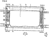
- the heat sink 10 is arranged in the vicinity of the side of the rectangular front housing 1 (rear housing 4) along arrow X2 to extend along the side in a direction Z (short-side direction of the front housing 1 (rear housing 4)) as viewed from behind, as shown in Figs. 3 and 6 . Further, the heat sink 10 is arranged on a region (region along arrow X2 in the outwardly exposed region 401) corresponding to the region 401 of the rear housing 4 exposed outward from the cover member 5 as viewed from behind.
- the heat sink 10 includes a first projecting portion 10c protruding toward the rear housing 4 and two second projecting portions 10d formed at a prescribed interval in the direction Z to hold the first projecting portion 10c therebetween.
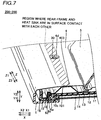
- an outer surface 101 of the first projecting portion 10c of the heat sink 10 is in the form of a planar surface.
- a portion of an inner surface 403 of the rear housing 4 corresponding to the first projecting portion 10c is also in the form of a planar surface.
- the outer surface 101 of the first projecting portion 10c of the heat sink 10 is arranged to be in surface contact with the inner surface 403 of the rear housing 4.
- the height (protrusion height with respect to the surface (rear surface) of the heat sink 10) H4 of the first projecting portion 10c is larger than the height (protrusion height with respect to the surface (rear surface) of the heat sink 10) H3 of the second projecting portions 10d of the heat sink 10.
- surfaces 102 of the second projecting portions 10d are in the form of planar surfaces.
- rear housing mounting threaded holes 10e for mounting the rear housing 4 are formed on the surfaces 102 of the second projecting portions 10d.
- Recess portions 4d concaved toward the second projecting portions 10d of the heat sink 10 are formed on portions of the rear housing 4 corresponding to the rear housing mounting threaded holes 10e of the second projecting portions 10d of the heat sink 10. Screw receiving holes 4e for mounting screws 30 are formed in the recess portions 4d of the rear housing 4.
- the screws 30 are mounted on the rear housing mounting threaded holes 10e of the second projecting portions 10d of the heat sink 10 through the screw receiving holes 4e of the read housing 4, thereby fixing (pressure-welding) surfaces 404 of the recess portions 4d of the rear housing 4 along arrow Y1 and the surfaces 102 of the second projecting portions 10d of the heat sink 10 along arrow Y2 to each other in a state in surface contact with each other.
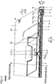
- Heat generated by the LED source 6a is radiated from the screws 30 and the outwardly exposed region 401 of the rear housing 4 through the heat sink 10 along a heat radiation path B shown in Fig. 9 .
- screw receiving holes 91c for mounting the reflection sheet holders 9a and 9b are formed in the reflection sheet holder 9c.
- Reflection sheet holder mounting threaded holes 92a and 92b for mounting the reflection sheet holder 9c are formed on the right ends of the reflection sheet holders 9a and 9b respectively.
- Screws 30 are mounted on the reflection sheet holder mounting threaded holes 92a and 92b of the reflection sheet holders 9a and 9b through the screw receiving holes 91c of the reflection sheet holder 9c, thereby fixing the reflection sheet holders 9a and 9b and the reflection sheet holder 9c to each other.
- screw receiving holes 92c for mounting the corresponding bezels 16 are formed on upper and lower end portions of the reflection sheet holder 9c respectively.
- Screws 30 are mounted on the bezel mounting threaded holes 93a and 93b formed on the right ends of the reflection sheet holders 9a and 9b through the screw receiving holes 16a of the bezels 16 and the screw receiving holes 92c on the upper and lower end portions of the reflection sheet holder 9c, thereby fixing the bezels 16 and the reflection sheet holders 9a, 9b and 9c to each other.
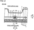
- the heating element 81 mounted on the circuit board 8 is mounted on the region 402 of the rear surface of the rear housing 4 covered with the cover member 5.
- the thermal pad 82 arranged between the circuit board 8 and the rear housing 4 is arranged to overlap with the heating element 81 of the circuit board 8 as viewed from behind. Further, the thermal pad 82 is formed to be smaller than the heating element 81 as viewed from behind.
- a rear surface (along arrow Y2) 41a of the thermal pad mounting portion 41 of the rear housing 4 is in the form of a planar surface. Further, the rear surface 41a of the thermal pad mounting portion 41 of the rear housing 4 is formed to be in surface contact with a front surface (along arrow Y1) 82a of the thermal pad 82. A rear surface (along arrow Y2) 82b of the thermal pad 82 is arranged to be in surface contact with a front surface (along arrow Y1) 80 of the circuit board 8.
- Heat generated by the heating element 81 mounted on the circuit board 8 is radiated from the outwardly exposed region 401 of the rear housing 4 through the thermal pad 82 and the thermal pad mounting portion 41 of the rear housing 4 along a heat radiation path C shown in Fig. 11 .
- the heat sink 10 is arranged on the region corresponding to the region 401 of the rear housing 4 exposed outward from the cover member 5 as viewed from behind.
- the heat generated by the LED source 6a can be excellently radiated from the outwardly exposed region 401 of the rear housing 4 through the heat sink 10, dissimilarly to a case where the heat sink 10 is arranged on the region 402 of the rear housing 4 covered with the cover member 5 as viewed from behind.
- the area of the region where the heat sink 10 is arranged can be reduced dissimilarly to a case where the heat sink 10 is arranged on a region substantially equal to the region where the rear housing 4 is arranged, for example. Consequently, the area of the region where the heat sink 10 is arranged can be reduced while excellently radiating the heat generated by the LED source 6a.
- the heat sink 10 mounted with the LED source 6a is arranged on the region corresponding to the region 401 of the rear housing 4 exposed outward from the cover member 5 as viewed from the side of the rear surface of the rear housing 4.
- the distance between the LED source 6a mounted on the heat sink 10 and the outwardly exposed region 401 of the rear housing 4 can be relatively reduced, whereby the heat generated by the LED source 6a can be quickly radiated from the outwardly exposed region 401 of the rear housing 4 through the heat sink 10.
- the surface 101 of the heat sink 10 closer to the rear housing 4 is arranged to be in surface contact with the inner surface 403 (404) of the rear housing 4.
- heat radiation can be more effectively performed as compared with a case where the surface 101 of the heat sink 10 closer to the rear housing 4 is arranged to be in point contact or in line contact with the inner surface 403 (404) of the rear housing 4.
- both of the surface 101 of the first projecting portion 10c of the heat sink 10 and the portion of the inner surface 403 of the rear housing 4 corresponding to the surface 101 of the first projecting portion 10c are in the form of planar surfaces.
- the surface 101 of the first projecting portion 10c of the heat sink 10 and the portion of the inner surface 403 of the rear housing 4 corresponding to the surface 101 of the first projecting portion 10c can be easily brought into surface contact with each other.
- the region where the surface 101 of the first projecting portion 10c of the heat sink 10 and the inner surface 403 of the rear housing 4 are in surface contact with each other is arranged in the vicinity of one side constituting the outer peripheral portion of the rectangularly formed rear housing 4 to extend along one side so that the region where the surface 101 of the first projecting portion 10c of the heat sink 10 and the inner surface 403 of the rear housing 4 are in surface contact with each other is arranged to extend along one side and the heat radiation area can be increased, whereby the heat radiation can be more effectively performed.
- the surfaces 102 of the second projecting portions 10d of the heat sink 10 mounted with the screws 30 and the surfaces 404 of the recess portions 4d of the rear housing 4 mounted with the screws 30 are fixed to each other with the screws 30 in the surface-contact state so that the surfaces 102 of the second projecting portions 10d of the heat sink 10 and the surfaces 404 of the recess portions 4d of the rear housing 4 can be pressure-welded to each other in the surface-contact state, whereby heat can be rendered more easily conductible, and the heat radiation can be more effectively performed as a result.
- all of the surfaces 102 of the second projecting portions 10d of the heat sink 10 and the surfaces 404 of the recess portions 4d of the rear housing 4 closer to the heat sink 10 are in the form of planar surfaces.
- the surfaces 102 of the second projecting portions 10d of the heat sink 10 and the surfaces 404 of the recess portions 4d of the rear housing 4 closer to the heat sink 10 can be easily brought into surface contact with each other.
- the protrusion height H4 of the first projecting portion 10c with respect to the surface (rear surface) of the heat sink 10 is rendered larger than the projection height H3 of the second projecting portions 10d with respect to the surface (rear surface) of the heat sink 10.
- the surface 101 of the first projecting portion 10c of the heat sink 10 and the portion of the inner surface 403 of the rear housing 4 corresponding to the surface 101 of the first projecting portion 10c come into surface contact with each other on the vertical position higher than that of the second projecting portions 10d, whereby the surface 101 of the first projecting portion 10c of the heat sink 10 and the portion of the inner surface 403 of the rear housing 4 corresponding to the surface 101 of the first projecting portion 10c can be easily brought into surface contact with each other while pressure-welding the surfaces 102 of the second projecting portions 10d of the heat sink 10 and the surfaces 404 of the recess portions 4d of the rear housing 4 closer to the heat sink 10 to each other in the surface-contact state.
- the backlight LED source 6a is so provided that the heat generated by the backlight LED source 6a can be excellently radiated from the outwardly exposed region 401 of the rear housing 4 through the heat sink 10.
- the thermal pad 82 for radiating the heat generated by the heating element 81 of the circuit board 8 to the rear housing 4 is so provided that the heat generated by the heating element 81 can be easily radiated from the outwardly exposed region 401 of the rear housing 4 through the thermal pad 82 also when the circuit board 8 mounted with the heating element 81 is covered with the cover member 5.
- the heat generated by the heating element 81 of the circuit board 8 covered with the cover member 5 is indirectly radiated from the outwardly exposed region 401 of the rear housing 4 through the thermal pad 82 and the thermal pad mounting portion 41 of the rear housing 4 so that the thickness of the thermal pad 82 can be reduced by the height of the thermal pad mounting portion 41 formed on the rear housing 4 and the heat generated by the heating element 81 is indirectly radiated from the outwardly exposed region 401 of the rear housing 4 through the thermal pad 82 and the thermal pad mounting portion 41 of the rear housing 4, whereby the heat generated by the heating element 81 can be easily radiated.
- the surface 41a of the thermal pad mounting portion 41 closer to the circuit board 8 is in the form of a planar surface.
- the thermal pad 82 can be easily fixed by arranging the thermal pad 82 in the clearance between the surface 41a of the thermal pad mounting portion 41 closer to the circuit board 8 and the circuit board 8 to be held therebetween.
- the protrusion height H1 of the board mounting portions 42 with respect to the rear surface of the rear housing 4 is rendered larger than the protrusion height H2 of the thermal pad mounting portion 41 with respect to the rear surface of the rear housing 4.
- the circuit board 8 is fixed on the vertical position higher than that of the thermal pad mounting portion 41, whereby the thermal pad 82 can be easily arranged in the clearance between the surface 41a of the thermal pad mounting portion 41 closer to the circuit board 8 and the circuit board 8 to be held therebetween.
- the heat sink 10 and the rear housing 4 made of metal are so provided that the heat generated by the LED source 6a or the heating element 81 can be rendered easily conductible, whereby heat radiation efficiency can be improved.
- the present invention is also applicable to another display such as a monitor of a personal computer other than the television set.
- the heat sink for radiating the heat generated by the light source portion is arranged to extend along the direction Z (short-side direction) of the rear housing in the aforementioned embodiment, the present invention is not restricted to this.
- the heat sink may alternatively be arranged to extend along the long-side direction of the rear housing, for example, so far as the same is arranged in the region of the rear housing exposed outward from the cover member as viewed from behind.
- the present invention is not restricted to this.
- the heat sink may alternatively be arranged to extend along two, three or four sides of the outer peripheral portion of the rear housing, for example, so far as the same is arranged in the region of the rear housing exposed outward from the cover member as viewed from behind.
- the area of the region where the heat sink is arranged can be reduced as compared with a case where the heat sink is provided on the overall surface of the rear housing. Further, heat radiation can be more effectively performed as compared with the case where the heat sink is arranged along one side of the outer peripheral portion of the rear housing.
- the present invention is not restricted to this.
- the heat sink or the rear housing may alternatively be made of a material, such as aluminum, for example, other than the sheet metal (SECC), so far as the same can radiate the heat generated by the LED source or the heat element.
- thermal pad made of the mixed material of silicone polymer and ceramic or the like is employed as an example of the second heat radiation member in the present invention in the aforementioned embodiment, the present invention is not restricted to this.
- a heat radiation member other than the thermal pad made of the mixed material of silicone polymer and ceramic or the like may alternatively be employed, for example, so far as the same can radiate the heat generated by the LED source or the heat element.
Landscapes
- Physics & Mathematics (AREA)
- Engineering & Computer Science (AREA)
- General Physics & Mathematics (AREA)
- Optics & Photonics (AREA)
- Microelectronics & Electronic Packaging (AREA)
- Nonlinear Science (AREA)
- Theoretical Computer Science (AREA)
- Crystallography & Structural Chemistry (AREA)
- Chemical & Material Sciences (AREA)
- Mathematical Physics (AREA)
- Thermal Sciences (AREA)
- Human Computer Interaction (AREA)
- General Engineering & Computer Science (AREA)
- Liquid Crystal (AREA)
- Planar Illumination Modules (AREA)
- Arrangement Of Elements, Cooling, Sealing, Or The Like Of Lighting Devices (AREA)
- Illuminated Signs And Luminous Advertising (AREA)
Claims (13)
- Anzeigevorrichtung, umfassend:eine Lichtführung (12) mit einer Lichtverteilungsplatte (13) und einer Linsenplatte (14) auf der Vorderseite und einer Reflexionsplatte (11) in der Rückseite,eine Flüssigkristallzelle (2), die vor der Lichtführung (12) angeordnet ist;einen Lichtquellenabschnitt (6a, 6b, 6c), der auf einem Seitenabschnitt der Lichtführung (12) angeordnet ist;ein erstes Wärmeabstrahlungselement (10), das auf der Rückseite der Lichtführung (12) angeordnet ist und in Kontakt mit dem Lichtquellenabschnitt (6a, 6b, 6c) steht;ein hinteres Gehäuse (4), das auf der Rückseite des ersten Wärmeabstrahlungselements (10) angeordnet ist, um das erste Wärmeabstrahlungselement (10) abzudecken; wobeidas erste Wärmeabstrahlungselement (10) einen ersten Vorsprungsabschnitt (10c) aufweist, der in Richtung einer Innenfläche (403) des hinteren Gehäuses (4) vorsteht, so dass ein Aussparungsabschnitt zwischen dem ersten Wärmeabstrahlungselement (10) und der Reflexionsplatte (10) vorhanden ist, wobei eine Außenfläche (101) des ersten Vorsprungsabschnitts (10c) des ersten Wärmeabstrahlungselements (10) in Oberflächenkontakt mit der Innenfläche des hinteren Gehäuses (4) steht,dadurch gekennzeichnet, dass die Anzeigevorrichtung des Weiteren umfasst:ein Abdeckungselement (5), das eine hintere Fläche des hinteren Gehäuses (4) teilweise abdeckt, so dass die hintere Fläche des hinteren Gehäuses (4) teilweise nach außen hin freiliegt, wobeidas erste Wärmeabstrahlungselement (10) mit der Reflexionsplatte (11) in einem Abschnitt zwischen einem Abschnitt, an dem der Lichtquellenabschnitt angeordnet ist und dem ersten Vorsprungsabschnitt (10c) in Kontakt steht, und in Kontakt mit der Reflexionsplatte (11) an einem Abschnitt steht, der sich von dem ersten Vorsprungsabschnitt (10c) in einer Richtung weg von dem Lichtquellenabschnitt erstreckt, wobeidas erste Wärmeabstrahlungselement (10) in einer Region (401) des hinteren Gehäuses angeordnet ist, die nach außen von dem Abdeckungselement (5) freigelegt ist.
- Anzeigevorrichtung nach Anspruch 1, wobei
der Lichtquellenabschnitt an dem ersten Wärmeabstrahlungselement (10) montiert ist, und
das erste Wärmeabstrahlungselement (10) mit dem daran montierten Lichtquellenabschnitt in der Region (401) des hinteren Gehäuses (4) angeordnet ist, die nach außen von dem Abdeckungselement freigelegt ist, betrachtet von der Seite der hinteren Fläche des hinteren Gehäuses (4). - Anzeigevorrichtung nach Anspruch 1, wobei
sowohl die äußere Fläche (101) des ersten Vorsprungsabschnitts (10c) des ersten Wärmeabstrahlungselements (10) als auch ein Abschnitt der inneren Fläche (403) des hinteren Gehäuses (4), der der äußeren Fläche (101) des ersten Vorsprungsabschnitts (10c) entspricht, die Form von planaren Flächen aufweisen. - Anzeigevorrichtung nach Anspruch 1, wobei
das hintere Gehäuse (4) rechtwinklig ausgebildet und so angeordnet ist, dass ein Abschnitt um einen Außenumfangsabschnitt des hinteren Gehäuses (4) herum nach außen von dem Abdeckungselement (5) in Form eines umgedrehten U freigelegt ist, und
eine Region, in der die äußere Fläche (101) des ersten Vorsprungsabschnitts (10c) des ersten Wärmeabstrahlungselements (10) und die innere Fläche (403) des hinteren Gehäuses (4) in Oberflächenkontakt miteinander stehen, auf einer Seite des Abschnitts um den Außenumfangsabschnitt des rechtwinklig ausgebildeten hinteren Gehäuses (4) herum angeordnet ist, so dass sie sich entlang der einen Seite erstreckt. - Anzeigevorrichtung nach Anspruch 1, wobei
das erste Wärmeabstrahlungselement (10) einen zweiten Vorsprungsabschnitt (10d) aufweist, der in Richtung der inneren Fläche des hinteren Gehäuses (4) vorsteht,
das hintere Gehäuse (4) einen Aussparungsabschnitt (4d) aufweist, der in Richtung des zweiten Vorsprungsabschnitts (10d) des ersten Wärmeabstrahlungselements (10) konkav ist, und
eine Oberfläche des zweiten Vorsprungsabschnitts (10d) und eine Oberfläche des Aussparungsabschnitts (4b) des hinteren Gehäuses (4) mithilfe eines Schraubenelements (30) aneinander fixiert sind, so dass sie miteinander in Oberflächenkontakt stehen. - Anzeigevorrichtung nach Anspruch 5, wobei
eine Vorsprungshöhe des ersten Vorsprungsabschnitts (10c) bezüglich einer Oberfläche des ersten Wärmeabstrahlungselements (10) größer als eine Vorsprungshöhe des zweiten Vorsprungsabschnitts (10d) bezüglich der Oberfläche des ersten Wärmeabstrahlungselements (10) ist. - Anzeigevorrichtung nach Anspruch 1, wobei
der Lichtquellenabschnitt eine Hinterleuchtungs-LED-Quelle beinhaltet. - Anzeigevorrichtung nach Anspruch 1, des Weiteren umfassend:eine Leiterplatte (8) mit einem Heizelement (81), das an einem Abschnitt der hinteren Fläche des hinteren Gehäuses (4) montiert ist, der mit dem Abdeckungselement (5) abgedeckt ist, undein zweites Wärmeabstrahlungselement (82), das zwischen der Leiterplatte und dem hinteren Gehäuse (4) angeordnet ist,wobei das zweite Wärmeabstrahlungselement (82) in Oberflächenkontakt sowohl mit einer vorderen Fläche (80) der Leiterplatte (8) als auch einer hinteren Fläche (41 a) eines dritten Vorsprungsabschnitts (41) des hinteren Gehäuses (4) steht.
- Anzeigevorrichtung nach Anspruch 8, wobei
der dritte Vorsprungsabschnitt (41), der in Richtung einer inneren Fläche des Abdeckungselements (5) vorsteht, an einer Region der hinteren Fläche des hinteren Gehäuses (4) entsprechend dem Heizelement der Leiterplatte angeordnet ist, wogegen das zweite Wärmeabstrahlungselement (82) zwischen der hinteren Fläche (41 a) des dritten Vorsprungsabschnitts (41) und der Leiterplatte (8) angeordnet ist, so dass es dazwischen gehalten wird, und
die Anzeigevorrichtung so ausgebildet ist, dass die Wärme, die von dem Heizelement der Leiterplatte erzeugt wird, die mit dem Abdeckungselement (5) abgedeckt ist, indirekt von der nach außen freiliegenden Region des hinteren Gehäuses (4) durch das zweite Wärmeabstrahlungselement (82) und den dritten Vorsprungsabschnitt des hinteren Gehäuses (4) abgestrahlt wird. - Anzeigevorrichtung nach Anspruch 1, wobei
das erste Wärmeabstrahlungselement (10) und das hintere Gehäuse (4) aus Metall bestehen. - Anzeigevorrichtung nach Anspruch 1, wobei
der Lichtquellenabschnitt (6a) so ausgebildet ist, dass eine Vielzahl von Lichtquellen entlang einer Seite angeordnet ist, die einen Außenumfangsabschnitt des hinteren Gehäuses (4) bildet, und sich das erste Wärmeabstrahlungselement (10) im Wesentlichen parallel entlang der Vielzahl von Lichtquellen erstreckt. - Anzeigevorrichtung nach Anspruch 1, wobei
der Aussparungsabschnitt eine Form aufweist, die sich von der Reflexionsplatte (11) in Richtung des hinteren Gehäuses (4) verjüngt. - Anzeigevorrichtung nach Anspruch 1, wobei das erste Wärmeabstrahlungselement (10) aus einem Blech besteht.
Priority Applications (1)
| Application Number | Priority Date | Filing Date | Title |
|---|---|---|---|
| EP17151425.0A EP3177127B1 (de) | 2011-10-12 | 2012-10-11 | Wärmeableitung über den hinteren rahmen eines displays |
Applications Claiming Priority (1)
| Application Number | Priority Date | Filing Date | Title |
|---|---|---|---|
| JP2011224559A JP5845795B2 (ja) | 2011-10-12 | 2011-10-12 | 表示装置 |
Related Child Applications (2)
| Application Number | Title | Priority Date | Filing Date |
|---|---|---|---|
| EP17151425.0A Division EP3177127B1 (de) | 2011-10-12 | 2012-10-11 | Wärmeableitung über den hinteren rahmen eines displays |
| EP17151425.0A Division-Into EP3177127B1 (de) | 2011-10-12 | 2012-10-11 | Wärmeableitung über den hinteren rahmen eines displays |
Publications (2)
| Publication Number | Publication Date |
|---|---|
| EP2582218A1 EP2582218A1 (de) | 2013-04-17 |
| EP2582218B1 true EP2582218B1 (de) | 2017-06-07 |
Family
ID=47257439
Family Applications (2)
| Application Number | Title | Priority Date | Filing Date |
|---|---|---|---|
| EP17151425.0A Not-in-force EP3177127B1 (de) | 2011-10-12 | 2012-10-11 | Wärmeableitung über den hinteren rahmen eines displays |
| EP12188067.8A Not-in-force EP2582218B1 (de) | 2011-10-12 | 2012-10-11 | Wärmeableitung über den Hinterrahmen einer Anzeigevorrichtung |
Family Applications Before (1)
| Application Number | Title | Priority Date | Filing Date |
|---|---|---|---|
| EP17151425.0A Not-in-force EP3177127B1 (de) | 2011-10-12 | 2012-10-11 | Wärmeableitung über den hinteren rahmen eines displays |
Country Status (3)
| Country | Link |
|---|---|
| US (5) | US9329434B2 (de) |
| EP (2) | EP3177127B1 (de) |
| JP (1) | JP5845795B2 (de) |
Families Citing this family (11)
| Publication number | Priority date | Publication date | Assignee | Title |
|---|---|---|---|---|
| US8616716B2 (en) * | 2009-10-20 | 2013-12-31 | Zhongliang Zheng | LED display screen assembled from the front |
| US9621838B2 (en) * | 2011-10-25 | 2017-04-11 | Funai Electric Co., Ltd. | Display device and television apparatus |
| US10048434B2 (en) * | 2012-11-08 | 2018-08-14 | Sharp Kabushiki Kaisha | Backlight device and liquid-crystal display device |
| USD776665S1 (en) * | 2015-02-05 | 2017-01-17 | Neonode Inc. | Light guide frame |
| US10409345B2 (en) * | 2015-03-23 | 2019-09-10 | Nec Corporation | Phase change cooling device and phase change cooling method |
| JP6570297B2 (ja) * | 2015-04-14 | 2019-09-04 | 株式会社nittoh | 照明モジュール |
| US9927642B2 (en) * | 2015-06-18 | 2018-03-27 | Ford Global Technologies, Llc | Vehicle display unit |
| JP6552919B2 (ja) * | 2015-08-27 | 2019-07-31 | Dynabook株式会社 | 電子機器 |
| CN109923602B (zh) * | 2017-08-09 | 2021-01-29 | 瑞仪(广州)光电子器件有限公司 | 框架组件及显示设备 |
| KR102845808B1 (ko) * | 2020-09-24 | 2025-08-13 | 삼성디스플레이 주식회사 | 표시 장치 및 이를 구비한 전자 기기 |
| KR102657348B1 (ko) * | 2021-08-31 | 2024-04-12 | 엘지전자 주식회사 | 디스플레이 디바이스 |
Citations (3)
| Publication number | Priority date | Publication date | Assignee | Title |
|---|---|---|---|---|
| JP2008130413A (ja) * | 2006-11-22 | 2008-06-05 | Epson Imaging Devices Corp | バックライトユニット及びこれを有する液晶表示装置 |
| WO2011083634A1 (ja) * | 2010-01-07 | 2011-07-14 | シャープ株式会社 | Led基板、バックライトユニットおよび液晶表示装置 |
| JP2011180287A (ja) * | 2010-02-26 | 2011-09-15 | Sharp Corp | 表示装置 |
Family Cites Families (24)
| Publication number | Priority date | Publication date | Assignee | Title |
|---|---|---|---|---|
| US7190424B2 (en) * | 2003-06-10 | 2007-03-13 | Samsung Electronics Co., Ltd. | Lamp wires of a liquid crystal display secured in trenches extending at an angle to a plate sidewall |
| JP2005084270A (ja) * | 2003-09-08 | 2005-03-31 | Sharp Corp | 薄型表示装置 |
| JP2005345855A (ja) | 2004-06-04 | 2005-12-15 | Pioneer Electronic Corp | 表示装置及びプラズマ表示装置 |
| KR101073043B1 (ko) * | 2004-11-16 | 2011-10-12 | 삼성전자주식회사 | 표시 장치 |
| JP3108915U (ja) * | 2004-11-22 | 2005-04-28 | 船井電機株式会社 | 液晶テレビジョンおよび液晶表示装置 |
| JP2006208485A (ja) | 2005-01-25 | 2006-08-10 | Alps Electric Co Ltd | 液晶表示装置及び電子機器 |
| JP4482473B2 (ja) * | 2005-03-25 | 2010-06-16 | シャープ株式会社 | 液晶表示装置 |
| CN101416101B (zh) * | 2006-04-10 | 2011-03-16 | 夏普株式会社 | 液晶显示装置 |
| KR20080008751A (ko) | 2006-07-21 | 2008-01-24 | 삼성전자주식회사 | 표시 장치 |
| KR101273592B1 (ko) | 2007-01-08 | 2013-06-11 | 삼성전자주식회사 | 패널형 디스플레이장치 |
| WO2008090646A1 (ja) * | 2007-01-22 | 2008-07-31 | Sharp Kabushiki Kaisha | バックライト装置、およびそれを用いた平面表示装置 |
| US8089582B2 (en) * | 2007-05-31 | 2012-01-03 | Hitachi Displays, Ltd. | Liquid crystal display device comprising at least one groove having an end portion that stops short of the non-adjacent opposite side surfaces and extends in a direction perpendicular to the non-adjacent side surfaces |
| JP2009098310A (ja) * | 2007-10-15 | 2009-05-07 | Hitachi Displays Ltd | 液晶表示装置 |
| JP2010009787A (ja) * | 2008-06-24 | 2010-01-14 | Toshiba Mobile Display Co Ltd | 照明ユニット及び照明ユニットを備えた液晶表示装置 |
| US7978286B2 (en) | 2008-06-24 | 2011-07-12 | Toshiba Mobile Display Co., Ltd. | Illumination unit and liquid crystal display device |
| US8355096B2 (en) * | 2008-08-04 | 2013-01-15 | Sharp Kabushiki Kaisha | Illumination device and liquid crystal display device including the same |
| JP2010054718A (ja) | 2008-08-27 | 2010-03-11 | Sony Corp | 表示装置 |
| JP2010113196A (ja) | 2008-11-07 | 2010-05-20 | Canon Inc | 画像表示装置 |
| KR101607572B1 (ko) * | 2009-10-12 | 2016-03-31 | 삼성디스플레이 주식회사 | 백라이트 어셈블리 및 그를 포함하는 표시 장치 |
| CN102246218A (zh) * | 2009-12-10 | 2011-11-16 | 松下电器产业株式会社 | 显示屏模块以及显示装置 |
| JP2011187312A (ja) * | 2010-03-09 | 2011-09-22 | Stanley Electric Co Ltd | サイドエッジ型面状発光装置 |
| KR101054767B1 (ko) | 2010-05-25 | 2011-08-05 | 엘지이노텍 주식회사 | 백라이트 유닛 및 표시장치 |
| KR101816275B1 (ko) * | 2010-12-23 | 2018-01-09 | 삼성디스플레이 주식회사 | 백라이트 어셈블리를 갖는 표시 장치 |
| JP5961942B2 (ja) * | 2011-08-04 | 2016-08-03 | セイコーエプソン株式会社 | 液晶表示装置および電子機器 |
-
2011
- 2011-10-12 JP JP2011224559A patent/JP5845795B2/ja not_active Expired - Fee Related
-
2012
- 2012-10-11 EP EP17151425.0A patent/EP3177127B1/de not_active Not-in-force
- 2012-10-11 EP EP12188067.8A patent/EP2582218B1/de not_active Not-in-force
- 2012-10-11 US US13/649,302 patent/US9329434B2/en active Active
-
2016
- 2016-04-06 US US15/091,879 patent/US9618691B2/en not_active Expired - Fee Related
-
2017
- 2017-03-29 US US15/472,980 patent/US9921366B2/en not_active Expired - Fee Related
- 2017-03-29 US US15/472,851 patent/US9910213B2/en not_active Expired - Fee Related
- 2017-03-29 US US15/473,035 patent/US9964695B2/en active Active
Patent Citations (3)
| Publication number | Priority date | Publication date | Assignee | Title |
|---|---|---|---|---|
| JP2008130413A (ja) * | 2006-11-22 | 2008-06-05 | Epson Imaging Devices Corp | バックライトユニット及びこれを有する液晶表示装置 |
| WO2011083634A1 (ja) * | 2010-01-07 | 2011-07-14 | シャープ株式会社 | Led基板、バックライトユニットおよび液晶表示装置 |
| JP2011180287A (ja) * | 2010-02-26 | 2011-09-15 | Sharp Corp | 表示装置 |
Also Published As
| Publication number | Publication date |
|---|---|
| US9618691B2 (en) | 2017-04-11 |
| US9964695B2 (en) | 2018-05-08 |
| US20160223740A1 (en) | 2016-08-04 |
| EP3177127B1 (de) | 2022-02-23 |
| JP2013084492A (ja) | 2013-05-09 |
| US20170199323A1 (en) | 2017-07-13 |
| US9921366B2 (en) | 2018-03-20 |
| US20130093959A1 (en) | 2013-04-18 |
| EP3177127A3 (de) | 2017-06-21 |
| US20170199324A1 (en) | 2017-07-13 |
| EP3177127A2 (de) | 2017-06-07 |
| US9329434B2 (en) | 2016-05-03 |
| EP2582218A1 (de) | 2013-04-17 |
| US20170199320A1 (en) | 2017-07-13 |
| JP5845795B2 (ja) | 2016-01-20 |
| US9910213B2 (en) | 2018-03-06 |
Similar Documents
| Publication | Publication Date | Title |
|---|---|---|
| EP2582218B1 (de) | Wärmeableitung über den Hinterrahmen einer Anzeigevorrichtung | |
| EP2587336B1 (de) | Anzeigevorrichtung | |
| EP2587303B1 (de) | Anzeigevorrichtung und Fernseher | |
| EP2587302B1 (de) | Anzeigevorrichtung und TV-Gerät | |
| JP2013101203A (ja) | 表示装置およびテレビジョン装置 | |
| US20180188446A1 (en) | Liquid crystal display | |
| US8970793B2 (en) | Display device, and television device | |
| JP2013092611A (ja) | 表示装置およびテレビジョン装置 | |
| JP5926905B2 (ja) | 表示装置およびテレビジョン装置 | |
| JP6741054B2 (ja) | 表示装置 | |
| JP6358291B2 (ja) | 表示装置 | |
| JP6111553B2 (ja) | 表示装置およびテレビジョン装置 | |
| JP5978591B2 (ja) | 表示装置 | |
| JP6409913B2 (ja) | 表示装置 | |
| EP2757866A1 (de) | Anzeigevorrichtung und Fernsehvorrichtung | |
| JP6168176B2 (ja) | 表示装置 | |
| JP2016149804A (ja) | 表示装置 |
Legal Events
| Date | Code | Title | Description |
|---|---|---|---|
| PUAI | Public reference made under article 153(3) epc to a published international application that has entered the european phase |
Free format text: ORIGINAL CODE: 0009012 |
|
| AK | Designated contracting states |
Kind code of ref document: A1 Designated state(s): AL AT BE BG CH CY CZ DE DK EE ES FI FR GB GR HR HU IE IS IT LI LT LU LV MC MK MT NL NO PL PT RO RS SE SI SK SM TR |
|
| AX | Request for extension of the european patent |
Extension state: BA ME |
|
| 17P | Request for examination filed |
Effective date: 20131007 |
|
| RBV | Designated contracting states (corrected) |
Designated state(s): AL AT BE BG CH CY CZ DE DK EE ES FI FR GB GR HR HU IE IS IT LI LT LU LV MC MK MT NL NO PL PT RO RS SE SI SK SM TR |
|
| 17Q | First examination report despatched |
Effective date: 20150331 |
|
| GRAP | Despatch of communication of intention to grant a patent |
Free format text: ORIGINAL CODE: EPIDOSNIGR1 |
|
| INTG | Intention to grant announced |
Effective date: 20160708 |
|
| GRAJ | Information related to disapproval of communication of intention to grant by the applicant or resumption of examination proceedings by the epo deleted |
Free format text: ORIGINAL CODE: EPIDOSDIGR1 |
|
| STAA | Information on the status of an ep patent application or granted ep patent |
Free format text: STATUS: EXAMINATION IS IN PROGRESS |
|
| GRAP | Despatch of communication of intention to grant a patent |
Free format text: ORIGINAL CODE: EPIDOSNIGR1 |
|
| STAA | Information on the status of an ep patent application or granted ep patent |
Free format text: STATUS: GRANT OF PATENT IS INTENDED |
|
| INTC | Intention to grant announced (deleted) | ||
| INTG | Intention to grant announced |
Effective date: 20161222 |
|
| GRAS | Grant fee paid |
Free format text: ORIGINAL CODE: EPIDOSNIGR3 |
|
| GRAA | (expected) grant |
Free format text: ORIGINAL CODE: 0009210 |
|
| STAA | Information on the status of an ep patent application or granted ep patent |
Free format text: STATUS: THE PATENT HAS BEEN GRANTED |
|
| AK | Designated contracting states |
Kind code of ref document: B1 Designated state(s): AL AT BE BG CH CY CZ DE DK EE ES FI FR GB GR HR HU IE IS IT LI LT LU LV MC MK MT NL NO PL PT RO RS SE SI SK SM TR |
|
| REG | Reference to a national code |
Ref country code: GB Ref legal event code: FG4D |
|
| GRAA | (expected) grant |
Free format text: ORIGINAL CODE: 0009210 |
|
| REG | Reference to a national code |
Ref country code: CH Ref legal event code: EP Ref country code: AT Ref legal event code: REF Ref document number: 900098 Country of ref document: AT Kind code of ref document: T Effective date: 20170615 |
|
| REG | Reference to a national code |
Ref country code: IE Ref legal event code: FG4D |
|
| REG | Reference to a national code |
Ref country code: DE Ref legal event code: R096 Ref document number: 602012033171 Country of ref document: DE |
|
| REG | Reference to a national code |
Ref country code: NL Ref legal event code: MP Effective date: 20170607 |
|
| REG | Reference to a national code |
Ref country code: LT Ref legal event code: MG4D |
|
| PG25 | Lapsed in a contracting state [announced via postgrant information from national office to epo] |
Ref country code: GR Free format text: LAPSE BECAUSE OF FAILURE TO SUBMIT A TRANSLATION OF THE DESCRIPTION OR TO PAY THE FEE WITHIN THE PRESCRIBED TIME-LIMIT Effective date: 20170908 Ref country code: HR Free format text: LAPSE BECAUSE OF FAILURE TO SUBMIT A TRANSLATION OF THE DESCRIPTION OR TO PAY THE FEE WITHIN THE PRESCRIBED TIME-LIMIT Effective date: 20170607 Ref country code: LT Free format text: LAPSE BECAUSE OF FAILURE TO SUBMIT A TRANSLATION OF THE DESCRIPTION OR TO PAY THE FEE WITHIN THE PRESCRIBED TIME-LIMIT Effective date: 20170607 Ref country code: FI Free format text: LAPSE BECAUSE OF FAILURE TO SUBMIT A TRANSLATION OF THE DESCRIPTION OR TO PAY THE FEE WITHIN THE PRESCRIBED TIME-LIMIT Effective date: 20170607 Ref country code: ES Free format text: LAPSE BECAUSE OF FAILURE TO SUBMIT A TRANSLATION OF THE DESCRIPTION OR TO PAY THE FEE WITHIN THE PRESCRIBED TIME-LIMIT Effective date: 20170607 Ref country code: NO Free format text: LAPSE BECAUSE OF FAILURE TO SUBMIT A TRANSLATION OF THE DESCRIPTION OR TO PAY THE FEE WITHIN THE PRESCRIBED TIME-LIMIT Effective date: 20170907 |
|
| REG | Reference to a national code |
Ref country code: AT Ref legal event code: MK05 Ref document number: 900098 Country of ref document: AT Kind code of ref document: T Effective date: 20170607 |
|
| PG25 | Lapsed in a contracting state [announced via postgrant information from national office to epo] |
Ref country code: NL Free format text: LAPSE BECAUSE OF FAILURE TO SUBMIT A TRANSLATION OF THE DESCRIPTION OR TO PAY THE FEE WITHIN THE PRESCRIBED TIME-LIMIT Effective date: 20170607 Ref country code: RS Free format text: LAPSE BECAUSE OF FAILURE TO SUBMIT A TRANSLATION OF THE DESCRIPTION OR TO PAY THE FEE WITHIN THE PRESCRIBED TIME-LIMIT Effective date: 20170607 Ref country code: SE Free format text: LAPSE BECAUSE OF FAILURE TO SUBMIT A TRANSLATION OF THE DESCRIPTION OR TO PAY THE FEE WITHIN THE PRESCRIBED TIME-LIMIT Effective date: 20170607 Ref country code: LV Free format text: LAPSE BECAUSE OF FAILURE TO SUBMIT A TRANSLATION OF THE DESCRIPTION OR TO PAY THE FEE WITHIN THE PRESCRIBED TIME-LIMIT Effective date: 20170607 Ref country code: BG Free format text: LAPSE BECAUSE OF FAILURE TO SUBMIT A TRANSLATION OF THE DESCRIPTION OR TO PAY THE FEE WITHIN THE PRESCRIBED TIME-LIMIT Effective date: 20170907 |
|
| PG25 | Lapsed in a contracting state [announced via postgrant information from national office to epo] |
Ref country code: SK Free format text: LAPSE BECAUSE OF FAILURE TO SUBMIT A TRANSLATION OF THE DESCRIPTION OR TO PAY THE FEE WITHIN THE PRESCRIBED TIME-LIMIT Effective date: 20170607 Ref country code: CZ Free format text: LAPSE BECAUSE OF FAILURE TO SUBMIT A TRANSLATION OF THE DESCRIPTION OR TO PAY THE FEE WITHIN THE PRESCRIBED TIME-LIMIT Effective date: 20170607 Ref country code: AT Free format text: LAPSE BECAUSE OF FAILURE TO SUBMIT A TRANSLATION OF THE DESCRIPTION OR TO PAY THE FEE WITHIN THE PRESCRIBED TIME-LIMIT Effective date: 20170607 Ref country code: RO Free format text: LAPSE BECAUSE OF FAILURE TO SUBMIT A TRANSLATION OF THE DESCRIPTION OR TO PAY THE FEE WITHIN THE PRESCRIBED TIME-LIMIT Effective date: 20170607 Ref country code: EE Free format text: LAPSE BECAUSE OF FAILURE TO SUBMIT A TRANSLATION OF THE DESCRIPTION OR TO PAY THE FEE WITHIN THE PRESCRIBED TIME-LIMIT Effective date: 20170607 |
|
| PG25 | Lapsed in a contracting state [announced via postgrant information from national office to epo] |
Ref country code: IS Free format text: LAPSE BECAUSE OF FAILURE TO SUBMIT A TRANSLATION OF THE DESCRIPTION OR TO PAY THE FEE WITHIN THE PRESCRIBED TIME-LIMIT Effective date: 20171007 Ref country code: SM Free format text: LAPSE BECAUSE OF FAILURE TO SUBMIT A TRANSLATION OF THE DESCRIPTION OR TO PAY THE FEE WITHIN THE PRESCRIBED TIME-LIMIT Effective date: 20170607 Ref country code: PL Free format text: LAPSE BECAUSE OF FAILURE TO SUBMIT A TRANSLATION OF THE DESCRIPTION OR TO PAY THE FEE WITHIN THE PRESCRIBED TIME-LIMIT Effective date: 20170607 Ref country code: IT Free format text: LAPSE BECAUSE OF FAILURE TO SUBMIT A TRANSLATION OF THE DESCRIPTION OR TO PAY THE FEE WITHIN THE PRESCRIBED TIME-LIMIT Effective date: 20170607 |
|
| REG | Reference to a national code |
Ref country code: DE Ref legal event code: R097 Ref document number: 602012033171 Country of ref document: DE |
|
| PLBE | No opposition filed within time limit |
Free format text: ORIGINAL CODE: 0009261 |
|
| STAA | Information on the status of an ep patent application or granted ep patent |
Free format text: STATUS: NO OPPOSITION FILED WITHIN TIME LIMIT |
|
| PG25 | Lapsed in a contracting state [announced via postgrant information from national office to epo] |
Ref country code: DK Free format text: LAPSE BECAUSE OF FAILURE TO SUBMIT A TRANSLATION OF THE DESCRIPTION OR TO PAY THE FEE WITHIN THE PRESCRIBED TIME-LIMIT Effective date: 20170607 |
|
| 26N | No opposition filed |
Effective date: 20180308 |
|
| PG25 | Lapsed in a contracting state [announced via postgrant information from national office to epo] |
Ref country code: MC Free format text: LAPSE BECAUSE OF FAILURE TO SUBMIT A TRANSLATION OF THE DESCRIPTION OR TO PAY THE FEE WITHIN THE PRESCRIBED TIME-LIMIT Effective date: 20170607 Ref country code: SI Free format text: LAPSE BECAUSE OF FAILURE TO SUBMIT A TRANSLATION OF THE DESCRIPTION OR TO PAY THE FEE WITHIN THE PRESCRIBED TIME-LIMIT Effective date: 20170607 |
|
| REG | Reference to a national code |
Ref country code: CH Ref legal event code: PL |
|
| GBPC | Gb: european patent ceased through non-payment of renewal fee |
Effective date: 20171011 |
|
| REG | Reference to a national code |
Ref country code: IE Ref legal event code: MM4A |
|
| REG | Reference to a national code |
Ref country code: FR Ref legal event code: ST Effective date: 20180629 |
|
| PG25 | Lapsed in a contracting state [announced via postgrant information from national office to epo] |
Ref country code: LI Free format text: LAPSE BECAUSE OF NON-PAYMENT OF DUE FEES Effective date: 20171031 Ref country code: GB Free format text: LAPSE BECAUSE OF NON-PAYMENT OF DUE FEES Effective date: 20171011 Ref country code: LU Free format text: LAPSE BECAUSE OF NON-PAYMENT OF DUE FEES Effective date: 20171011 Ref country code: CH Free format text: LAPSE BECAUSE OF NON-PAYMENT OF DUE FEES Effective date: 20171031 |
|
| REG | Reference to a national code |
Ref country code: BE Ref legal event code: MM Effective date: 20171031 |
|
| PG25 | Lapsed in a contracting state [announced via postgrant information from national office to epo] |
Ref country code: BE Free format text: LAPSE BECAUSE OF NON-PAYMENT OF DUE FEES Effective date: 20171031 Ref country code: FR Free format text: LAPSE BECAUSE OF NON-PAYMENT OF DUE FEES Effective date: 20171031 |
|
| PG25 | Lapsed in a contracting state [announced via postgrant information from national office to epo] |
Ref country code: MT Free format text: LAPSE BECAUSE OF NON-PAYMENT OF DUE FEES Effective date: 20171011 |
|
| PG25 | Lapsed in a contracting state [announced via postgrant information from national office to epo] |
Ref country code: IE Free format text: LAPSE BECAUSE OF NON-PAYMENT OF DUE FEES Effective date: 20171011 |
|
| PG25 | Lapsed in a contracting state [announced via postgrant information from national office to epo] |
Ref country code: HU Free format text: LAPSE BECAUSE OF FAILURE TO SUBMIT A TRANSLATION OF THE DESCRIPTION OR TO PAY THE FEE WITHIN THE PRESCRIBED TIME-LIMIT; INVALID AB INITIO Effective date: 20121011 |
|
| PG25 | Lapsed in a contracting state [announced via postgrant information from national office to epo] |
Ref country code: CY Free format text: LAPSE BECAUSE OF NON-PAYMENT OF DUE FEES Effective date: 20170607 |
|
| PG25 | Lapsed in a contracting state [announced via postgrant information from national office to epo] |
Ref country code: MK Free format text: LAPSE BECAUSE OF FAILURE TO SUBMIT A TRANSLATION OF THE DESCRIPTION OR TO PAY THE FEE WITHIN THE PRESCRIBED TIME-LIMIT Effective date: 20170607 |
|
| PG25 | Lapsed in a contracting state [announced via postgrant information from national office to epo] |
Ref country code: TR Free format text: LAPSE BECAUSE OF FAILURE TO SUBMIT A TRANSLATION OF THE DESCRIPTION OR TO PAY THE FEE WITHIN THE PRESCRIBED TIME-LIMIT Effective date: 20170607 |
|
| PG25 | Lapsed in a contracting state [announced via postgrant information from national office to epo] |
Ref country code: PT Free format text: LAPSE BECAUSE OF FAILURE TO SUBMIT A TRANSLATION OF THE DESCRIPTION OR TO PAY THE FEE WITHIN THE PRESCRIBED TIME-LIMIT Effective date: 20170607 |
|
| PG25 | Lapsed in a contracting state [announced via postgrant information from national office to epo] |
Ref country code: AL Free format text: LAPSE BECAUSE OF FAILURE TO SUBMIT A TRANSLATION OF THE DESCRIPTION OR TO PAY THE FEE WITHIN THE PRESCRIBED TIME-LIMIT Effective date: 20170607 |
|
| PGFP | Annual fee paid to national office [announced via postgrant information from national office to epo] |
Ref country code: DE Payment date: 20230830 Year of fee payment: 12 |
|
| REG | Reference to a national code |
Ref country code: DE Ref legal event code: R119 Ref document number: 602012033171 Country of ref document: DE |
|
| PG25 | Lapsed in a contracting state [announced via postgrant information from national office to epo] |
Ref country code: DE Free format text: LAPSE BECAUSE OF NON-PAYMENT OF DUE FEES Effective date: 20250501 |