EP2575162B1 - Herstellungsverfahren einer Halbleitervorrichtung mit einer selektiven Schwindungsphase einer Silizium-Germanium-Schicht - Google Patents
Herstellungsverfahren einer Halbleitervorrichtung mit einer selektiven Schwindungsphase einer Silizium-Germanium-Schicht Download PDFInfo
- Publication number
- EP2575162B1 EP2575162B1 EP12185100.0A EP12185100A EP2575162B1 EP 2575162 B1 EP2575162 B1 EP 2575162B1 EP 12185100 A EP12185100 A EP 12185100A EP 2575162 B1 EP2575162 B1 EP 2575162B1
- Authority
- EP
- European Patent Office
- Prior art keywords
- silicon
- layer
- germanium
- solution
- seconds
- Prior art date
- Legal status (The legal status is an assumption and is not a legal conclusion. Google has not performed a legal analysis and makes no representation as to the accuracy of the status listed.)
- Active
Links
Images

Classifications
-
- H—ELECTRICITY
- H10—SEMICONDUCTOR DEVICES; ELECTRIC SOLID-STATE DEVICES NOT OTHERWISE PROVIDED FOR
- H10P—GENERIC PROCESSES OR APPARATUS FOR THE MANUFACTURE OR TREATMENT OF DEVICES COVERED BY CLASS H10
- H10P50/00—Etching of wafers, substrates or parts of devices
- H10P50/60—Wet etching
- H10P50/64—Wet etching of semiconductor materials
- H10P50/642—Chemical etching
-
- H—ELECTRICITY
- H10—SEMICONDUCTOR DEVICES; ELECTRIC SOLID-STATE DEVICES NOT OTHERWISE PROVIDED FOR
- H10D—INORGANIC ELECTRIC SEMICONDUCTOR DEVICES
- H10D84/00—Integrated devices formed in or on semiconductor substrates that comprise only semiconducting layers, e.g. on Si wafers or on GaAs-on-Si wafers
- H10D84/01—Manufacture or treatment
- H10D84/0123—Integrating together multiple components covered by H10D12/00 or H10D30/00, e.g. integrating multiple IGBTs
- H10D84/0126—Integrating together multiple components covered by H10D12/00 or H10D30/00, e.g. integrating multiple IGBTs the components including insulated gates, e.g. IGFETs
- H10D84/0165—Integrating together multiple components covered by H10D12/00 or H10D30/00, e.g. integrating multiple IGBTs the components including insulated gates, e.g. IGFETs the components including complementary IGFETs, e.g. CMOS devices
- H10D84/0167—Manufacturing their channels
-
- H—ELECTRICITY
- H10—SEMICONDUCTOR DEVICES; ELECTRIC SOLID-STATE DEVICES NOT OTHERWISE PROVIDED FOR
- H10D—INORGANIC ELECTRIC SEMICONDUCTOR DEVICES
- H10D84/00—Integrated devices formed in or on semiconductor substrates that comprise only semiconducting layers, e.g. on Si wafers or on GaAs-on-Si wafers
- H10D84/01—Manufacture or treatment
- H10D84/02—Manufacture or treatment characterised by using material-based technologies
- H10D84/03—Manufacture or treatment characterised by using material-based technologies using Group IV technology, e.g. silicon technology or silicon-carbide [SiC] technology
- H10D84/038—Manufacture or treatment characterised by using material-based technologies using Group IV technology, e.g. silicon technology or silicon-carbide [SiC] technology using silicon technology, e.g. SiGe
-
- H—ELECTRICITY
- H10—SEMICONDUCTOR DEVICES; ELECTRIC SOLID-STATE DEVICES NOT OTHERWISE PROVIDED FOR
- H10P—GENERIC PROCESSES OR APPARATUS FOR THE MANUFACTURE OR TREATMENT OF DEVICES COVERED BY CLASS H10
- H10P50/00—Etching of wafers, substrates or parts of devices
- H10P50/60—Wet etching
- H10P50/66—Wet etching of conductive or resistive materials
- H10P50/663—Wet etching of conductive or resistive materials by chemical means only
- H10P50/667—Wet etching of conductive or resistive materials by chemical means only by liquid etching only
-
- H—ELECTRICITY
- H10—SEMICONDUCTOR DEVICES; ELECTRIC SOLID-STATE DEVICES NOT OTHERWISE PROVIDED FOR
- H10P—GENERIC PROCESSES OR APPARATUS FOR THE MANUFACTURE OR TREATMENT OF DEVICES COVERED BY CLASS H10
- H10P70/00—Cleaning of wafers, substrates or parts of devices
- H10P70/20—Cleaning during device manufacture
-
- C—CHEMISTRY; METALLURGY
- C09—DYES; PAINTS; POLISHES; NATURAL RESINS; ADHESIVES; COMPOSITIONS NOT OTHERWISE PROVIDED FOR; APPLICATIONS OF MATERIALS NOT OTHERWISE PROVIDED FOR
- C09K—MATERIALS FOR MISCELLANEOUS APPLICATIONS, NOT PROVIDED FOR ELSEWHERE
- C09K13/00—Etching, surface-brightening or pickling compositions
-
- H—ELECTRICITY
- H10—SEMICONDUCTOR DEVICES; ELECTRIC SOLID-STATE DEVICES NOT OTHERWISE PROVIDED FOR
- H10P—GENERIC PROCESSES OR APPARATUS FOR THE MANUFACTURE OR TREATMENT OF DEVICES COVERED BY CLASS H10
- H10P50/00—Etching of wafers, substrates or parts of devices
- H10P50/20—Dry etching; Plasma etching; Reactive-ion etching
- H10P50/28—Dry etching; Plasma etching; Reactive-ion etching of insulating materials
- H10P50/282—Dry etching; Plasma etching; Reactive-ion etching of insulating materials of inorganic materials
- H10P50/283—Dry etching; Plasma etching; Reactive-ion etching of insulating materials of inorganic materials by chemical means
Definitions
- the present invention relates to a method of manufacturing a semiconductor device with a step of selective removal of a silicon-germanium layer.
- the PMOS is masked by a layer of resin so as to be protected. Then, silicon-germanium must be removed locally, through the resin mask in the areas to receive an NMOS. This removal of the silicon-germanium must be selective with respect to the lower layers and the resin.
- US 2006/068557 A1 discloses a method of removing a silicon-germanium layer by exposure to an etching solution comprising hydrofluoric acid, hydrogen peroxide, and acetic acid.
- US 7132322 B1 discloses a method of removing a silicon-germanium layer by exposure to an etching solution comprising hydrogen peroxide, and ammonia. There is therefore the need to propose a method for eliminating a silicon-germanium layer by wet process and preferentially with a selectivity satisfactory and without significantly damaging a resin mask.
- the present invention relates to a method of manufacturing a semiconductor device by wet chemical etching, the device comprising at least one silicon layer (Si) and at least one silicon-germanium layer (SiGe) and at least one layer of photosensitive resin forming a mask partially covering the layer of silicon germanium (SiGe) and leaving free the layer of silicon germanium in certain zones characterized in that it comprises a step of removing the silicon-germanium (SiGe) layer at said zones by exposure to an etching solution.
- the etching solution having a pH of between 3 and 6 is formed by a manufacturing step from hydrofluoric acid (HF), hydrogen peroxide (H 2 O 2 ), acetic acid (CH 3 COOH). ) and ammonia (NH 4 OH).
- the combination of these four components in the etching solution makes it possible to obtain a preferentially selective removal step of the germanium silicon layer.
- the pH of the etching solution is studied both to be compatible with a resin mask and both to allow selective removal of the silicon germanium layer. Indeed, for a man of the art these objectives seem, a priori, opposite; the pH not to damage a resin, is advantageously around 3 to 6 while to obtain a selective shrinkage, the amount of etching species must be maximum or around a pH of 1 to 2.
- the etching solution according to the invention is diluted between 5 and 500 times.
- This dilution brings many benefits including control of etching speed and better etching.
- the dilution factor is calculated based on the total volume of the etching solution before dilution.
- the method according to the invention allows a removal of the silicon-germanium zones with a very good selectivity vis-à-vis the other layers of the transistor and without damaging, or little, the resin mask.
- the method comprises at least one pre-treatment step and / or one post-treatment step respectively before and after the withdrawal step.
- the solutions used for the pre-treatment stage and the post-treatment stage are produced by mixing hydrofluoric acid (HF) and ammonia (NH 4 OH).
- This method of preparation leads to a buffered solution having a pH in accordance with use with a resin mask, ie from 3 to 6 and advantageously with selectivity towards silicon-germanium.
- the semiconductor device manufactured by the present method comprises at least one transistor.
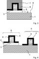
- the device preferably comprises a silicon 1 or silicon on insulator (Silicon On Insulator) substrate plate.
- a germanium silicon layer 2 is deposited on the silicon substrate 1.
- the silicon-germanium 2 preferentially forms the channel of the PMOS transistor 6.
- the PMOS transistor 6 comprises a gate 4, for example made of poly silicon or metal, surrounded by and others of spacers 5, for example silicon oxide or silicon nitride. Between the gate 4 and the silicon-germanium layer 2 is a layer of silicon oxide 3 or a high permittivity material called "high k" such as HfO2, HfSiO, HfZrO2, Al2O3.
- the resin 2 is then removed at the zones 8 between the PMOS transistors 6.
- the silicon-germanium layer 2 at the zones 8 is exposed so as to allow its partial or total removal.
- NMOS transistor 9 It is in these areas 8 that the NMOS transistor 9 will be formed.
- the total removal of the silicon-germanium layer 2 at the zones 8 is preferred.
- an etching solution is used to remove the silicon-germanium layer 2.
- a pre-treatment solution can be applied before the removal of this silicon-germanium layer 2.
- a post-treatment solution can be applied after the removal of this silicon-germanium layer 2.
- the NMOS transistor 9 is formed on a silicon 1 or silicon on insulator (silicon on insulator) substrate and comprises a grid 4, for example made of poly silicon or metal, surrounded by and others of spacers. 5, for example in silicon oxide or silicon nitride. Between the gate 4 and the silicon-germanium layer 2 is a layer of silicon oxide 3 or a high permittivity material called "high k" such as HfO2, HfSiO, HfZrO2, Al2O3.
- high k high permittivity material
- the removal in at least some zones 8 of the silicon-germanium layer 2 in a transistor must have a high selectivity.
- the evolution of microelectronics tends in particular to reduce the size of the nodes between the transistors, current research aims to obtain nodes smaller than 30 nanometers.
- the SOI substrate 1 is generalized and in this case the upper silicon thickness is critical, the etching of the silicon-germanium layer 2 must be highly selective so as not to etch the silicon of the substrate 1. It is then essential that the sharpness of the shrinkage is maximal without damaging or weakly the resin 7.
- the etching solution is prepared by mixing hydrofluoric acid (HF), hydrogen peroxide (H 2 O 2 ), acetic acid (CH 3 COOH) and ammonia (NH 4). 4 OH).
- the etching solution is prepared with a ratio between the four initial components being 1/2/3/4 respectively of HF / H 2 O 2 / CH 3 COOH / NH 4 OH.
- Ammonia (NH 4 OH) in a larger quantity makes it possible to neutralize the acids namely hydrofluoric acid (HF) and acetic acid (CH 3 COOH).
- HF hydrofluoric acid
- CH 3 COOH acetic acid
- the solution thus formed is a buffered solution, it has the property of keeping its pH stable over a certain dilution range.
- the dilution is advantageously carried out with deionized water.
- the dilution of the solution is preferably between 5 and 500 times, preferably 20 to 100 times.
- the method according to the invention allows a selectivity of the step of removing the silicon-germanium layer 2 from the silicon layer 1 of between 4/1 and 50/1 for germanium silicon layers ranging from 5 to 60% germanium, preferably 10 to 60%.
- An etching solution is prepared according to the following information without dilution: HF / H2O2 / CH3COOH / NH4OH in ratios of 1/2/3/4 without addition of deionized water for dilution.
- etching solution is prepared according to the amounts below. The concentrations of the various components are close to those of Example 1. v (HF) V (H2O2) v (CH3COOH) v (NH4OH) v (DI) Vtotal pH 10 20 30 40 100 200 4.03
- the etching solution has a high exothermicity. Since the etching rate is too high, the selectivity of the solution can not be calculated.
- the thickness removed from the silicon and silicon-germanium layers is controlled.
- the etching solution contains components forming oxidizing species namely hydrogen peroxide (H2O2) and acetic acid (CH 3 COOH) which form per acetic acid (CH3CO3H) with high oxidizing power.
- H2O2 hydrogen peroxide
- CH 3 COOH acetic acid
- CH3CO3H per acetic acid
- ammonia increases the pH of the etching solution and removes it from an efficient etching but ammonia (NH 4 OH) reacts notably with hydrofluoric acid (HF) to form ammonium fluoride (NH4F) in the ammonium ion / fluoride ion (NH4 + / F-) form which contributes to the etching of the silicon germanium by the formation of hydrogen difluoride (HF2-) between the hydrofluoric acid (HF) and the ion fluoride (F-).
- HF hydrofluoric acid
- the oxidation and etching phenomena succeed one another in a repetitive manner.
- the duration of the exposure of the pretreatment stage is from 20 to 300 seconds, preferably from 30 to 120 seconds, advantageously of the order of 40 seconds.
- the pretreatment solution has a pH of preferably between 3 and 5, advantageously of the order of 3. It advantageously contains hydrofluoric acid (HF).
- the pretreatment solution advantageously has a ratio of NH4F / HF ranging from 2/1 to 500/1, preferentially from 2/1 to 30/1, more preferably from 2/1 to 6/1.
- the duration of the exposure of the post-treatment step is between 10 and 180 seconds, preferably from 20 to 60 seconds and advantageously of the order of 20 seconds.
- the post-treatment solution is preferably identical to the pretreatment solution described above.
- the method comprises a pretreatment step of a duration of the order of 30 to 90 seconds, preferably of the order of 60 seconds, a step of withdrawal of a duration of the order of 30 to 180 seconds. seconds preferably of the order of 60 to 120 seconds and a post-processing step of a duration of the order of 20 to 90 seconds preferably of the order of 20 to 60 seconds.
- the ratio of ammonia fluoride (NH4F) / hydrofluoric acid (HF) is 3/1 for a pH of 3.48.
- the pretreatment, withdrawal and post-treatment steps are carried out successively with respective durations of 60 seconds on the following samples: either silicon or layers of silicon germanium at different concentrations: 28 nm SiGe 30% - 53 nmSiGe 10% - 75nm SiGe 20% - 40nm SiGe 40% - 26nm SiGe 50%. Samples Engraving (nm) 45nm Si 0.9 53nm SiGe 10% 1.2 75nm SiGe 20% 2 28nm SiGe 30% All (28) 40nm SiGe 40% All (40)
- a selectivity of the order of 30/1 is obtained for the 30% germanium silicon layer.
- the etching rate is 120 Angstrom / minute or 12 nm for 30% silicon germanium.
- the etching rate can be decreased if it is desired not to remove the entire silicon germanium layer. Otherwise, the burn time is reduced to limit the shrinkage.
Landscapes
- Weting (AREA)
- Chemical & Material Sciences (AREA)
- Chemical Kinetics & Catalysis (AREA)
- General Chemical & Material Sciences (AREA)
- Cleaning Or Drying Semiconductors (AREA)
Claims (15)
- Verfahren zum Herstellen einer Halbleitervorrichtung durch chemisches Nassätzen, wobei die Vorrichtung zumindest eine Schicht aus Silicium (Si) und zumindest eine Schicht aus Silicium-Germanium (SiG2) (2) und zumindest eine lichtempfindliche Harzschicht (7) enthält, die eine die Schicht aus Silicium-Germanium (SiGe) (2) teilweise überdeckende und die Schicht aus Silicium-Germanium in bestimmen Bereichen (9) freilassende Maske bildet,
wobei das Verfahren einen Schritt des Herstellens einer Ätzlösung mit einem pH-Wert zwischen 3 und 6 ausgehend von Fluorwasserstoffsäure (HF), Wasserstoffperoxid (H2O2), Essigsäure (CH3COOH) und Ammoniak (NH4OH) umfasst sowie einen Schritt des Entfernens der Schicht aus Silicium-Germanium (SiGe) (2) in Höhe der genannten Bereiche (8), indem sie der Ätzlösung ausgesetzt wird. - Verfahren nach dem vorangehenden Anspruch, wobei der pH-Wert der Ätzlösung zwischen 3,5 und 4 beträgt.
- Verfahren nach einem der vorangehenden Ansprüche, wobei das Herstellen der Ätzlösung ausgehend von 49 %-iger Fluorwasserstoffsäure (HF), Wasserstoffperoxid (H2O2), 100 %-iger Essigsäure (CH3COOH) und 28 %-igem Ammoniak (NH4OH) jeweils im Volumenverhältnis 1:2:3:4 erfolgt.
- Verfahren nach einem der vorangehenden Ansprüche, wobei bei dem Schritt des Herstellens die Ätzlösung in entionisiertem Wasser 5- bis 500-mal verdünnt wird.
- Verfahren nach einem der vorangehenden Ansprüche, wobei die Dauer des Aussetzens der Ätzlösung zwischen 20 Sekunden und 600 Sekunden beträgt.
- Verfahren nach einem der vorangehenden Ansprüche, wobei die Dauer des Aussetzens der Ätzlösung zwischen 30 Sekunden und 120 Sekunden beträgt.
- Verfahren nach einem der vorangehenden Ansprüche, umfassend vor dem Schritt des Entfernens einen Schritt der Vorbehandlung, umfassend einen Schritt des Herstellens einer Vorbehandlungslösung ausgehend von 48 %-iger Fluorwasserstoffsäure (HF) und 29 %-igem Ammoniak (NH4OH), vorzugsweise derart, dass ein Volumenverhältnis NH4F/HF von 2:1 bis 6:1 und ein Aussetzen zumindest der Bereiche (8) der Schicht aus Silicium-Germanium (SiGe) (2) einer Vorbehandlungslösung, so dass das Anlaufen des Schritts des Entfernens erleichtert wird.
- Verfahren nach dem vorangehenden Anspruch, wobei die Dauer des Aussetzens der Vorbehandlungslösung zwischen 20 Sekunden und 300 Sekunden beträgt.
- Verfahren nach einem der beiden vorangehenden Ansprüche, wobei die Dauer des Aussetzens der Vorbehandlungslösung zwischen 30 Sekunden und 120 Sekunden beträgt.
- Verfahren nach einem der vorangehenden Ansprüche, umfassend einen Schritt des Herstellens einer Nachbehandlungslösung ausgehend von 48 %-iger Fluorwasserstoffsäure (HF) und 29 %-igem Ammoniak (NH4OH), vorzugsweise derart, dass ein Volumenverhältnis NH4F/HF von 2:1 bis 6:1 erhalten wird, sowie nach dem Schritt des Entfernens einen Nachbehandlungsschritt durch Aussetzen zumindest der Bereiche (8) der Schicht aus Silicium-Germanium (SiGe) (2) einer Nachbehandlungslösung, so dass der Oberflächenzustand der Schicht verbessert wird, die unter den Entfernungsbereichen (8) liegt, indem eventuell vorhandene Verunreinigungen entfernt werden.
- Verfahren nach dem vorangehenden Anspruch, wobei die Dauer des Aussetzens der Nachbehandlungslösung zwischen 10 Sekunden und 180 Sekunden beträgt.
- Verfahren nach einem der beiden vorangehenden Ansprüche, wobei die Dauer des Aussetzens der Nachbehandlungslösung zwischen 20 Sekunden und 60 Sekunden beträgt.
- Verfahren nach einem der vorangehenden Ansprüche, wobei die Schicht aus Silicium-Germanium (SiGe) einen Prozentsatz an Germanium von 5 bis 60 % enthält.
- Verfahren nach einem der vorangehenden Ansprüche, wobei die Schicht aus Silicium-Germanium (SiGe) einen Transistorkanal bildet.
- Verfahren nach einem der vorangehenden Ansprüche, wobei der Schritt des Entfernens der Schicht aus Silicium-Germanium (SiGe) (2) so erfolgt, dass die Schicht aus Silicium-Germanium (SiGe) (2) an den Bereichen (8) vollständig entfernt wird, wobei die Schicht aus Silicium (Si) (1) in diesen Bereichen (8) freigelegt wird.
Applications Claiming Priority (1)
| Application Number | Priority Date | Filing Date | Title |
|---|---|---|---|
| FR1158674A FR2980637B1 (fr) | 2011-09-28 | 2011-09-28 | Procede de fabrication d'un dispositif semi-conducteur avec une etape de retrait selective d'une couche de silicium germanium |
Publications (3)
| Publication Number | Publication Date |
|---|---|
| EP2575162A2 EP2575162A2 (de) | 2013-04-03 |
| EP2575162A3 EP2575162A3 (de) | 2014-04-02 |
| EP2575162B1 true EP2575162B1 (de) | 2018-05-23 |
Family
ID=46829677
Family Applications (1)
| Application Number | Title | Priority Date | Filing Date |
|---|---|---|---|
| EP12185100.0A Active EP2575162B1 (de) | 2011-09-28 | 2012-09-19 | Herstellungsverfahren einer Halbleitervorrichtung mit einer selektiven Schwindungsphase einer Silizium-Germanium-Schicht |
Country Status (3)
| Country | Link |
|---|---|
| US (1) | US9076732B2 (de) |
| EP (1) | EP2575162B1 (de) |
| FR (1) | FR2980637B1 (de) |
Families Citing this family (10)
| Publication number | Priority date | Publication date | Assignee | Title |
|---|---|---|---|---|
| WO2014178426A1 (ja) * | 2013-05-02 | 2014-11-06 | 富士フイルム株式会社 | エッチング方法、これに用いるエッチング液およびエッチング液のキット、ならびに半導体基板製品の製造方法 |
| FR3031835B1 (fr) | 2015-01-16 | 2017-12-22 | Commissariat Energie Atomique | Procede de realisation d'un circuit electronique integre tridimensionnel |
| CN107851660B (zh) * | 2015-07-09 | 2022-02-01 | 恩特格里斯公司 | 相对于锗选择性蚀刻硅锗的调配物 |
| CR20180165A (es) * | 2015-08-21 | 2018-06-14 | Ecolab Usa Inc | Complejación y eliminación del mercurio de sistema de desulfuración de gas de combustión |
| US10043672B2 (en) * | 2016-03-29 | 2018-08-07 | Lam Research Corporation | Selective self-aligned patterning of silicon germanium, germanium and type III/V materials using a sulfur-containing mask |
| KR102710507B1 (ko) * | 2016-12-14 | 2024-09-25 | 삼성전자주식회사 | 식각용 조성물 및 이를 이용한 반도체 장치 제조 방법 |
| KR102880474B1 (ko) | 2019-07-08 | 2025-11-03 | 바스프 에스이 | 실리콘-게르마늄 재료를 선택적으로 에칭하기 위한 조성물, 그의 용도 및 방법 |
| KR20230065325A (ko) * | 2020-09-11 | 2023-05-11 | 후지필름 일렉트로닉 머티리얼스 유.에스.에이., 아이엔씨. | 에칭 조성물 |
| EP4257658A3 (de) * | 2022-04-04 | 2024-02-28 | Samsung Electronics Co., Ltd. | Ätzzusammensetzung, verfahren zum ätzen eines metallhaltigen films unter verwendung derselben und verfahren zur herstellung eines halbleiterbauelements damit |
| CN115763546B (zh) * | 2022-11-01 | 2025-10-10 | 长鑫存储技术有限公司 | 半导体结构及其制备方法 |
Family Cites Families (4)
| Publication number | Priority date | Publication date | Assignee | Title |
|---|---|---|---|---|
| WO2005013375A1 (ja) * | 2003-08-05 | 2005-02-10 | Fujitsu Limited | 半導体装置及びその製造方法 |
| KR100607176B1 (ko) * | 2004-03-25 | 2006-08-01 | 삼성전자주식회사 | 희석 에이.피.엠 수용액을 이용한 반도체 장치의 제조방법들 |
| KR100585148B1 (ko) * | 2004-06-22 | 2006-05-30 | 삼성전자주식회사 | 실리콘 저매늄 희생층을 이용한 반도체 소자의 미세 패턴형성방법 및 그 패턴 형성방법을 이용한 자기정렬 콘택형성방법 |
| US7132322B1 (en) * | 2005-05-11 | 2006-11-07 | International Business Machines Corporation | Method for forming a SiGe or SiGeC gate selectively in a complementary MIS/MOS FET device |
-
2011
- 2011-09-28 FR FR1158674A patent/FR2980637B1/fr not_active Expired - Fee Related
-
2012
- 2012-09-19 EP EP12185100.0A patent/EP2575162B1/de active Active
- 2012-09-27 US US13/628,318 patent/US9076732B2/en active Active
Non-Patent Citations (1)
| Title |
|---|
| None * |
Also Published As
| Publication number | Publication date |
|---|---|
| FR2980637B1 (fr) | 2014-05-16 |
| US20130109191A1 (en) | 2013-05-02 |
| EP2575162A3 (de) | 2014-04-02 |
| US9076732B2 (en) | 2015-07-07 |
| EP2575162A2 (de) | 2013-04-03 |
| FR2980637A1 (fr) | 2013-03-29 |
Similar Documents
| Publication | Publication Date | Title |
|---|---|---|
| EP2575162B1 (de) | Herstellungsverfahren einer Halbleitervorrichtung mit einer selektiven Schwindungsphase einer Silizium-Germanium-Schicht | |
| EP3072149B1 (de) | Verfahren zur selektiven ätzung einer auf einem siliciumsubstrat abgelagerten maske | |
| EP1051744B1 (de) | Verfahren zur herstellung eines halbleiterbauelements | |
| EP0887843B1 (de) | Verfahren zur Herstellung eines Transistors mit einem Silizium-Germanium-Gatter | |
| EP3144973B1 (de) | Verfahren zur bildung von abstandhaltern eines gates eines transistors | |
| US20020142616A1 (en) | Method for improved fabrication of salicide structures | |
| JP2007123903A (ja) | 選択的に高k材をエッチングするためのプラズマ組成 | |
| TWI463535B (zh) | 形成半導體層之方法 | |
| EP0780889A2 (de) | Verfahren zu selektiver Abscheidung von Feuerfestmetall-Silizid über Silizium sowie durch dieses Verfahren metallizierte Siliziumwafer | |
| WO1999043024A1 (fr) | Procede pour limiter l'interdiffusion dans un dispositif semi-conducteur a grill composite si/sige | |
| EP1811549B1 (de) | Verfahren zur selektiven Entfernung von nicht silizidiertem Metall | |
| CN1317743C (zh) | 用于制造半导体器件的方法 | |
| WO1999043023A1 (fr) | Procede de nitruration de la couche d'oxyde de grille d'un dispositif semiconducteur et dispositif obtenu | |
| CN103000520A (zh) | Mos表面栅极侧壁层的刻蚀方法 | |
| US6908805B2 (en) | Method of manufacturing dual gate oxide film | |
| CN1577753A (zh) | 制造半导体器件的栅电极的方法 | |
| FR2957458A1 (fr) | Procede de realisation d’une electrode conductrice | |
| CN105990234B (zh) | 半导体器件的形成方法 | |
| TWI251281B (en) | Method for implementing poly pre-doping in deep sub-micron process | |
| KR100546397B1 (ko) | 게이트 씨닝을 방지할 수 있는 씨모스 트랜지스터의제조방법 | |
| FR2974446A1 (fr) | Procédé de réalisation de l'isolant de grille d'un transistor mos | |
| CN104009037A (zh) | 半导体器件及其制造方法 | |
| JP4471986B2 (ja) | 半導体装置の製造方法 | |
| WO2026017561A1 (fr) | Procédé de réalisation d'un dispositif à transistors cfet | |
| EP2657956A1 (de) | Behandlungsverfahren des Oberflächenzustands eines Siliziumsubstrats |
Legal Events
| Date | Code | Title | Description |
|---|---|---|---|
| PUAI | Public reference made under article 153(3) epc to a published international application that has entered the european phase |
Free format text: ORIGINAL CODE: 0009012 |
|
| AK | Designated contracting states |
Kind code of ref document: A2 Designated state(s): AL AT BE BG CH CY CZ DE DK EE ES FI FR GB GR HR HU IE IS IT LI LT LU LV MC MK MT NL NO PL PT RO RS SE SI SK SM TR |
|
| AX | Request for extension of the european patent |
Extension state: BA ME |
|
| PUAL | Search report despatched |
Free format text: ORIGINAL CODE: 0009013 |
|
| AK | Designated contracting states |
Kind code of ref document: A3 Designated state(s): AL AT BE BG CH CY CZ DE DK EE ES FI FR GB GR HR HU IE IS IT LI LT LU LV MC MK MT NL NO PL PT RO RS SE SI SK SM TR |
|
| AX | Request for extension of the european patent |
Extension state: BA ME |
|
| RIC1 | Information provided on ipc code assigned before grant |
Ipc: H01L 21/306 20060101AFI20140221BHEP Ipc: H01L 21/8238 20060101ALI20140221BHEP |
|
| 17P | Request for examination filed |
Effective date: 20140925 |
|
| RBV | Designated contracting states (corrected) |
Designated state(s): AL AT BE BG CH CY CZ DE DK EE ES FI FR GB GR HR HU IE IS IT LI LT LU LV MC MK MT NL NO PL PT RO RS SE SI SK SM TR |
|
| GRAP | Despatch of communication of intention to grant a patent |
Free format text: ORIGINAL CODE: EPIDOSNIGR1 |
|
| STAA | Information on the status of an ep patent application or granted ep patent |
Free format text: STATUS: GRANT OF PATENT IS INTENDED |
|
| INTG | Intention to grant announced |
Effective date: 20171220 |
|
| GRAS | Grant fee paid |
Free format text: ORIGINAL CODE: EPIDOSNIGR3 |
|
| GRAA | (expected) grant |
Free format text: ORIGINAL CODE: 0009210 |
|
| STAA | Information on the status of an ep patent application or granted ep patent |
Free format text: STATUS: THE PATENT HAS BEEN GRANTED |
|
| AK | Designated contracting states |
Kind code of ref document: B1 Designated state(s): AL AT BE BG CH CY CZ DE DK EE ES FI FR GB GR HR HU IE IS IT LI LT LU LV MC MK MT NL NO PL PT RO RS SE SI SK SM TR |
|
| REG | Reference to a national code |
Ref country code: GB Ref legal event code: FG4D Free format text: NOT ENGLISH |
|
| REG | Reference to a national code |
Ref country code: CH Ref legal event code: EP |
|
| REG | Reference to a national code |
Ref country code: IE Ref legal event code: FG4D Free format text: LANGUAGE OF EP DOCUMENT: FRENCH |
|
| REG | Reference to a national code |
Ref country code: DE Ref legal event code: R096 Ref document number: 602012046558 Country of ref document: DE |
|
| REG | Reference to a national code |
Ref country code: AT Ref legal event code: REF Ref document number: 1002183 Country of ref document: AT Kind code of ref document: T Effective date: 20180615 |
|
| REG | Reference to a national code |
Ref country code: NL Ref legal event code: MP Effective date: 20180523 |
|
| REG | Reference to a national code |
Ref country code: FR Ref legal event code: PLFP Year of fee payment: 7 |
|
| REG | Reference to a national code |
Ref country code: LT Ref legal event code: MG4D |
|
| PG25 | Lapsed in a contracting state [announced via postgrant information from national office to epo] |
Ref country code: NO Free format text: LAPSE BECAUSE OF FAILURE TO SUBMIT A TRANSLATION OF THE DESCRIPTION OR TO PAY THE FEE WITHIN THE PRESCRIBED TIME-LIMIT Effective date: 20180823 Ref country code: FI Free format text: LAPSE BECAUSE OF FAILURE TO SUBMIT A TRANSLATION OF THE DESCRIPTION OR TO PAY THE FEE WITHIN THE PRESCRIBED TIME-LIMIT Effective date: 20180523 Ref country code: BG Free format text: LAPSE BECAUSE OF FAILURE TO SUBMIT A TRANSLATION OF THE DESCRIPTION OR TO PAY THE FEE WITHIN THE PRESCRIBED TIME-LIMIT Effective date: 20180823 Ref country code: SE Free format text: LAPSE BECAUSE OF FAILURE TO SUBMIT A TRANSLATION OF THE DESCRIPTION OR TO PAY THE FEE WITHIN THE PRESCRIBED TIME-LIMIT Effective date: 20180523 Ref country code: LT Free format text: LAPSE BECAUSE OF FAILURE TO SUBMIT A TRANSLATION OF THE DESCRIPTION OR TO PAY THE FEE WITHIN THE PRESCRIBED TIME-LIMIT Effective date: 20180523 Ref country code: ES Free format text: LAPSE BECAUSE OF FAILURE TO SUBMIT A TRANSLATION OF THE DESCRIPTION OR TO PAY THE FEE WITHIN THE PRESCRIBED TIME-LIMIT Effective date: 20180523 |
|
| PG25 | Lapsed in a contracting state [announced via postgrant information from national office to epo] |
Ref country code: NL Free format text: LAPSE BECAUSE OF FAILURE TO SUBMIT A TRANSLATION OF THE DESCRIPTION OR TO PAY THE FEE WITHIN THE PRESCRIBED TIME-LIMIT Effective date: 20180523 Ref country code: RS Free format text: LAPSE BECAUSE OF FAILURE TO SUBMIT A TRANSLATION OF THE DESCRIPTION OR TO PAY THE FEE WITHIN THE PRESCRIBED TIME-LIMIT Effective date: 20180523 Ref country code: HR Free format text: LAPSE BECAUSE OF FAILURE TO SUBMIT A TRANSLATION OF THE DESCRIPTION OR TO PAY THE FEE WITHIN THE PRESCRIBED TIME-LIMIT Effective date: 20180523 Ref country code: LV Free format text: LAPSE BECAUSE OF FAILURE TO SUBMIT A TRANSLATION OF THE DESCRIPTION OR TO PAY THE FEE WITHIN THE PRESCRIBED TIME-LIMIT Effective date: 20180523 Ref country code: GR Free format text: LAPSE BECAUSE OF FAILURE TO SUBMIT A TRANSLATION OF THE DESCRIPTION OR TO PAY THE FEE WITHIN THE PRESCRIBED TIME-LIMIT Effective date: 20180824 |
|
| REG | Reference to a national code |
Ref country code: AT Ref legal event code: MK05 Ref document number: 1002183 Country of ref document: AT Kind code of ref document: T Effective date: 20180523 |
|
| PG25 | Lapsed in a contracting state [announced via postgrant information from national office to epo] |
Ref country code: EE Free format text: LAPSE BECAUSE OF FAILURE TO SUBMIT A TRANSLATION OF THE DESCRIPTION OR TO PAY THE FEE WITHIN THE PRESCRIBED TIME-LIMIT Effective date: 20180523 Ref country code: PL Free format text: LAPSE BECAUSE OF FAILURE TO SUBMIT A TRANSLATION OF THE DESCRIPTION OR TO PAY THE FEE WITHIN THE PRESCRIBED TIME-LIMIT Effective date: 20180523 Ref country code: AT Free format text: LAPSE BECAUSE OF FAILURE TO SUBMIT A TRANSLATION OF THE DESCRIPTION OR TO PAY THE FEE WITHIN THE PRESCRIBED TIME-LIMIT Effective date: 20180523 Ref country code: CZ Free format text: LAPSE BECAUSE OF FAILURE TO SUBMIT A TRANSLATION OF THE DESCRIPTION OR TO PAY THE FEE WITHIN THE PRESCRIBED TIME-LIMIT Effective date: 20180523 Ref country code: RO Free format text: LAPSE BECAUSE OF FAILURE TO SUBMIT A TRANSLATION OF THE DESCRIPTION OR TO PAY THE FEE WITHIN THE PRESCRIBED TIME-LIMIT Effective date: 20180523 Ref country code: DK Free format text: LAPSE BECAUSE OF FAILURE TO SUBMIT A TRANSLATION OF THE DESCRIPTION OR TO PAY THE FEE WITHIN THE PRESCRIBED TIME-LIMIT Effective date: 20180523 Ref country code: SK Free format text: LAPSE BECAUSE OF FAILURE TO SUBMIT A TRANSLATION OF THE DESCRIPTION OR TO PAY THE FEE WITHIN THE PRESCRIBED TIME-LIMIT Effective date: 20180523 |
|
| REG | Reference to a national code |
Ref country code: DE Ref legal event code: R097 Ref document number: 602012046558 Country of ref document: DE |
|
| PG25 | Lapsed in a contracting state [announced via postgrant information from national office to epo] |
Ref country code: SM Free format text: LAPSE BECAUSE OF FAILURE TO SUBMIT A TRANSLATION OF THE DESCRIPTION OR TO PAY THE FEE WITHIN THE PRESCRIBED TIME-LIMIT Effective date: 20180523 Ref country code: IT Free format text: LAPSE BECAUSE OF FAILURE TO SUBMIT A TRANSLATION OF THE DESCRIPTION OR TO PAY THE FEE WITHIN THE PRESCRIBED TIME-LIMIT Effective date: 20180523 |
|
| PLBE | No opposition filed within time limit |
Free format text: ORIGINAL CODE: 0009261 |
|
| STAA | Information on the status of an ep patent application or granted ep patent |
Free format text: STATUS: NO OPPOSITION FILED WITHIN TIME LIMIT |
|
| PG25 | Lapsed in a contracting state [announced via postgrant information from national office to epo] |
Ref country code: MC Free format text: LAPSE BECAUSE OF FAILURE TO SUBMIT A TRANSLATION OF THE DESCRIPTION OR TO PAY THE FEE WITHIN THE PRESCRIBED TIME-LIMIT Effective date: 20180523 |
|
| REG | Reference to a national code |
Ref country code: CH Ref legal event code: PL |
|
| 26N | No opposition filed |
Effective date: 20190226 |
|
| GBPC | Gb: european patent ceased through non-payment of renewal fee |
Effective date: 20180919 |
|
| PG25 | Lapsed in a contracting state [announced via postgrant information from national office to epo] |
Ref country code: SI Free format text: LAPSE BECAUSE OF FAILURE TO SUBMIT A TRANSLATION OF THE DESCRIPTION OR TO PAY THE FEE WITHIN THE PRESCRIBED TIME-LIMIT Effective date: 20180523 |
|
| REG | Reference to a national code |
Ref country code: BE Ref legal event code: MM Effective date: 20180930 |
|
| REG | Reference to a national code |
Ref country code: IE Ref legal event code: MM4A |
|
| PG25 | Lapsed in a contracting state [announced via postgrant information from national office to epo] |
Ref country code: LU Free format text: LAPSE BECAUSE OF NON-PAYMENT OF DUE FEES Effective date: 20180919 |
|
| PG25 | Lapsed in a contracting state [announced via postgrant information from national office to epo] |
Ref country code: IE Free format text: LAPSE BECAUSE OF NON-PAYMENT OF DUE FEES Effective date: 20180919 |
|
| PG25 | Lapsed in a contracting state [announced via postgrant information from national office to epo] |
Ref country code: BE Free format text: LAPSE BECAUSE OF NON-PAYMENT OF DUE FEES Effective date: 20180930 Ref country code: LI Free format text: LAPSE BECAUSE OF NON-PAYMENT OF DUE FEES Effective date: 20180930 Ref country code: CH Free format text: LAPSE BECAUSE OF NON-PAYMENT OF DUE FEES Effective date: 20180930 |
|
| PG25 | Lapsed in a contracting state [announced via postgrant information from national office to epo] |
Ref country code: GB Free format text: LAPSE BECAUSE OF NON-PAYMENT OF DUE FEES Effective date: 20180919 |
|
| PG25 | Lapsed in a contracting state [announced via postgrant information from national office to epo] |
Ref country code: AL Free format text: LAPSE BECAUSE OF FAILURE TO SUBMIT A TRANSLATION OF THE DESCRIPTION OR TO PAY THE FEE WITHIN THE PRESCRIBED TIME-LIMIT Effective date: 20180523 |
|
| PG25 | Lapsed in a contracting state [announced via postgrant information from national office to epo] |
Ref country code: MT Free format text: LAPSE BECAUSE OF FAILURE TO SUBMIT A TRANSLATION OF THE DESCRIPTION OR TO PAY THE FEE WITHIN THE PRESCRIBED TIME-LIMIT Effective date: 20180523 |
|
| PG25 | Lapsed in a contracting state [announced via postgrant information from national office to epo] |
Ref country code: TR Free format text: LAPSE BECAUSE OF FAILURE TO SUBMIT A TRANSLATION OF THE DESCRIPTION OR TO PAY THE FEE WITHIN THE PRESCRIBED TIME-LIMIT Effective date: 20180523 |
|
| PG25 | Lapsed in a contracting state [announced via postgrant information from national office to epo] |
Ref country code: PT Free format text: LAPSE BECAUSE OF FAILURE TO SUBMIT A TRANSLATION OF THE DESCRIPTION OR TO PAY THE FEE WITHIN THE PRESCRIBED TIME-LIMIT Effective date: 20180523 Ref country code: HU Free format text: LAPSE BECAUSE OF FAILURE TO SUBMIT A TRANSLATION OF THE DESCRIPTION OR TO PAY THE FEE WITHIN THE PRESCRIBED TIME-LIMIT; INVALID AB INITIO Effective date: 20120919 |
|
| PG25 | Lapsed in a contracting state [announced via postgrant information from national office to epo] |
Ref country code: MK Free format text: LAPSE BECAUSE OF NON-PAYMENT OF DUE FEES Effective date: 20180523 Ref country code: CY Free format text: LAPSE BECAUSE OF FAILURE TO SUBMIT A TRANSLATION OF THE DESCRIPTION OR TO PAY THE FEE WITHIN THE PRESCRIBED TIME-LIMIT Effective date: 20180523 |
|
| PG25 | Lapsed in a contracting state [announced via postgrant information from national office to epo] |
Ref country code: IS Free format text: LAPSE BECAUSE OF FAILURE TO SUBMIT A TRANSLATION OF THE DESCRIPTION OR TO PAY THE FEE WITHIN THE PRESCRIBED TIME-LIMIT Effective date: 20180923 |
|
| PGFP | Annual fee paid to national office [announced via postgrant information from national office to epo] |
Ref country code: DE Payment date: 20250919 Year of fee payment: 14 |
|
| PGFP | Annual fee paid to national office [announced via postgrant information from national office to epo] |
Ref country code: FR Payment date: 20250924 Year of fee payment: 14 |
|
| REG | Reference to a national code |
Ref country code: DE Ref legal event code: R079 Ref document number: 602012046558 Country of ref document: DE Free format text: PREVIOUS MAIN CLASS: H01L0021306000 Ipc: H10P0050000000 |