EP2567412B1 - Light emitting diode package with rounded rectangular lens - Google Patents
Light emitting diode package with rounded rectangular lens Download PDFInfo
- Publication number
- EP2567412B1 EP2567412B1 EP11721828.9A EP11721828A EP2567412B1 EP 2567412 B1 EP2567412 B1 EP 2567412B1 EP 11721828 A EP11721828 A EP 11721828A EP 2567412 B1 EP2567412 B1 EP 2567412B1
- Authority
- EP
- European Patent Office
- Prior art keywords
- lens
- led die
- package
- led
- width
- Prior art date
- Legal status (The legal status is an assumption and is not a legal conclusion. Google has not performed a legal analysis and makes no representation as to the accuracy of the status listed.)
- Active
Links
- 239000002184 metal Substances 0.000 description 6
- 239000004065 semiconductor Substances 0.000 description 5
- 229920001296 polysiloxane Polymers 0.000 description 3
- 239000000919 ceramic Substances 0.000 description 2
- 230000007704 transition Effects 0.000 description 2
- OAICVXFJPJFONN-UHFFFAOYSA-N Phosphorus Chemical compound [P] OAICVXFJPJFONN-UHFFFAOYSA-N 0.000 description 1
- 239000011248 coating agent Substances 0.000 description 1
- 238000000576 coating method Methods 0.000 description 1
- 230000001419 dependent effect Effects 0.000 description 1
- 239000000463 material Substances 0.000 description 1
- 238000000034 method Methods 0.000 description 1
- 238000012986 modification Methods 0.000 description 1
- 230000004048 modification Effects 0.000 description 1
- 238000005476 soldering Methods 0.000 description 1
- 239000007787 solid Substances 0.000 description 1
- 239000012780 transparent material Substances 0.000 description 1
Images

Classifications
-
- H—ELECTRICITY
- H01—ELECTRIC ELEMENTS
- H01L—SEMICONDUCTOR DEVICES NOT COVERED BY CLASS H10
- H01L33/00—Semiconductor devices having potential barriers specially adapted for light emission; Processes or apparatus specially adapted for the manufacture or treatment thereof or of parts thereof; Details thereof
- H01L33/48—Semiconductor devices having potential barriers specially adapted for light emission; Processes or apparatus specially adapted for the manufacture or treatment thereof or of parts thereof; Details thereof characterised by the semiconductor body packages
- H01L33/58—Optical field-shaping elements
-
- G—PHYSICS
- G02—OPTICS
- G02B—OPTICAL ELEMENTS, SYSTEMS OR APPARATUS
- G02B19/00—Condensers, e.g. light collectors or similar non-imaging optics
- G02B19/0004—Condensers, e.g. light collectors or similar non-imaging optics characterised by the optical means employed
- G02B19/0009—Condensers, e.g. light collectors or similar non-imaging optics characterised by the optical means employed having refractive surfaces only
- G02B19/0014—Condensers, e.g. light collectors or similar non-imaging optics characterised by the optical means employed having refractive surfaces only at least one surface having optical power
-
- G—PHYSICS
- G02—OPTICS
- G02B—OPTICAL ELEMENTS, SYSTEMS OR APPARATUS
- G02B19/00—Condensers, e.g. light collectors or similar non-imaging optics
- G02B19/0033—Condensers, e.g. light collectors or similar non-imaging optics characterised by the use
- G02B19/0047—Condensers, e.g. light collectors or similar non-imaging optics characterised by the use for use with a light source
- G02B19/0061—Condensers, e.g. light collectors or similar non-imaging optics characterised by the use for use with a light source the light source comprising a LED
-
- H—ELECTRICITY
- H01—ELECTRIC ELEMENTS
- H01L—SEMICONDUCTOR DEVICES NOT COVERED BY CLASS H10
- H01L33/00—Semiconductor devices having potential barriers specially adapted for light emission; Processes or apparatus specially adapted for the manufacture or treatment thereof or of parts thereof; Details thereof
- H01L33/48—Semiconductor devices having potential barriers specially adapted for light emission; Processes or apparatus specially adapted for the manufacture or treatment thereof or of parts thereof; Details thereof characterised by the semiconductor body packages
- H01L33/52—Encapsulations
- H01L33/54—Encapsulations having a particular shape
-
- H—ELECTRICITY
- H01—ELECTRIC ELEMENTS
- H01L—SEMICONDUCTOR DEVICES NOT COVERED BY CLASS H10
- H01L2924/00—Indexing scheme for arrangements or methods for connecting or disconnecting semiconductor or solid-state bodies as covered by H01L24/00
- H01L2924/0001—Technical content checked by a classifier
- H01L2924/0002—Not covered by any one of groups H01L24/00, H01L24/00 and H01L2224/00
-
- H—ELECTRICITY
- H01—ELECTRIC ELEMENTS
- H01L—SEMICONDUCTOR DEVICES NOT COVERED BY CLASS H10
- H01L33/00—Semiconductor devices having potential barriers specially adapted for light emission; Processes or apparatus specially adapted for the manufacture or treatment thereof or of parts thereof; Details thereof
- H01L33/48—Semiconductor devices having potential barriers specially adapted for light emission; Processes or apparatus specially adapted for the manufacture or treatment thereof or of parts thereof; Details thereof characterised by the semiconductor body packages
- H01L33/483—Containers
- H01L33/486—Containers adapted for surface mounting
Definitions
- This invention relates to light emitting diode (LED) packages and, in particular, to an LED package having a rounded square lens that emits a substantially Lambertian emission pattern.
- LED light emitting diode
- FIG. 1 is a top perspective view an LED package 10 copied from the present assignee's US design patent no. D598,871 .
- the commercial name for the package is the RebelTM.
- the package 10 is about 3mm per side.
- the package 10 contains a square LED die whose sides are aligned with the sides of the package 10.
- the center axis of the LED die is along the center axis of the hemispherical lens 12.
- Anode and cathode electrodes are on the bottom surface of the package 10 for soldering to metal pads on a printed circuit board.
- Anode and cathode electrodes formed on the LED semiconductor layers are electrically connected to the anode and cathode electrodes on the bottom of the package.
- the LED layers are mounted on a submount, and the submount electrodes are, in turn, connected to the package electrodes. LEDs and submounts are described in detail in US patent no. 7,452,737 .
- the emitted light pattern is substantially Lambertian, which forms a circle on a flat surface directly above the package 10.
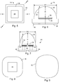
- Fig. 2 is a top down view of the package 10 showing the alignment of the LED die 14 with the lens 12 and package 10.
- Fig. 3 is a side view of the package 10 along the diagonal line 3-3 in Fig. 2 .
- the hemispherical lens 12 has a diameter about 2.55mm, and the LED die 14 is about 1mm per side. The diagonal length of the LED die is about 1.4mm.
- the edges of the actual LED die 14 are shown by solid lines. Since the lens 12 is a hemisphere referenced to the top surface of the LED die 14, light rays 15 emitted from the center point 16 of the LED die 14 at all angles impinge on the surface of the lens 12 at substantially right angles, so the light rays 15 are emitted from the package 10 with virtually no internal reflection and no refraction.
- the size of the package 10 and lens 12 are designed for an LED die 14 having maximum sides of about 1mm to substantially prevent any light rays from being internally reflected by the lens 12.
- Fig. 3 illustrates an extension of the LED die 14 in dashed outline and a light ray 18 emitted near the corner of the enlarged LED die.
- the angle of the light ray 18 is less than the critical angle, resulting in total internal reflection (TIR) of the light ray 18.
- TIR total internal reflection
- the width of a square LED die for use with the package 10 is limited to about 1mm (the solid outline of the die 14) in order to minimize TIR.
- Fig. 4 is a top perspective view of another prior art package 20 by the assignee having the same width and lens 12 as the package 10 of Fig. 1 but a longer length.
- the diameter of the lens 12 is limited by the width of the package 20.
- the electrode footprint and outer dimensions of the "higher output” package need to be the same as those for the existing package 10.
- the substantially Lambertian emission pattern also needs to be substantially the same. Although a larger width LED die may be used to emit more light, there will be TIR within the hemispherical lens 12 if a larger LED die is used, greatly reducing the efficiency of the package. The diameter of the hemispherical lens 12 cannot be increased without increasing the width of the package 10.
- JP 2010 050236 A discloses a semiconductor light emitting device with a sub-mount, a semiconductor light emitting element mounted on the sub-mount, and a light-transparent enveloping layer completely covering the semiconductor light emitting element and acting as a lens.
- the light-transparent enveloping layer is formed in contact with the entire planar outer circumference of the sub-mount.
- the present inventor was faced with the problem of generating more light out of an existing package ( Fig. 1 or 4 ).
- the package size (footprint) could not be changed.
- the inventor solved the problem with the present invention.
- the present invention is directed to an LED device in accordance with the appended claim 1.
- Advantageous embodiments of the present invention are the object of the appended dependent claims 2-10.
- a rounded square lens is used instead of the hemispherical lens 12 in the package of Fig. 1 or 4 , where the width of the rounded square lens is the same as the diameter of the hemispherical lens 12 to allow the rounded square lens to fit within the package 10.
- a cross-sectional view of the rounded square lens cut along its diagonal forms a semicircular surface so as to emulate a hemispherical lens along the diagonal and areas close to the diagonal.
- a cross-sectional view of the lens cut along its width bisecting the lens forms a narrower bullet shaped surface having the same height as the semicircular surface. The four corners of the lens are rounded. The surface of the lens smoothly transitions between the two surface shapes.
- the resulting light pattern is substantially Lambertian (substantially similar to the light emission of a hemispherical lens used with a square LED die), forming a substantially circular pattern on a flat surface above the package rather than a square pattern.
- the rounded square lens has a diagonal dimension that is larger than the maximum diameter of a hemispherical lens in the package, a larger LED die may be used with the rounded square lens.
- a larger LED die may be used with the rounded square lens.
- more light is emitted using the larger LED die with little or no TIR, no increase in the package size, and no apparent change in the Lambertian light pattern.
- an LED die having sides of up to 1.4mm may be used in the new package, versus a maximum width LED die of about 1. 1mm in the prior art package 10. This doubles the light emitting top surface area of the LED die.
- the new package having the rounded square lens may replace the old package 10 in a camera flash application, doubling the light output with no change in the camera design.
- the shape of the lens below the top surface of the LED die is not very significant since little light is emitted below the top surface. Therefore, the shape of the lens below the top surface may have sharper corners, flanges, or other features that better enable the lens to be affixed to the package body.
- the LED dies may be flip-chips, or have top and bottom electrodes, or have top electrodes only.
- FIG. 5-8 illustrate the invention.
- the body 22 of the package 24 may be ceramic, plastic, silicone, or other material.
- the outer dimensions of the body 22 may be exactly the same as the outer dimensions of the prior art package 10 or 20 bodies, and the electrode structure may be exactly the same, so the package 24 may be substituted for the package 10 or 20 in any application.
- the only difference is the size of the LED die 26 and the lens 28.
- the LED die 26, in one example, includes LED semiconductor layers mounted on a ceramic submount having a metal pattern, and electrodes on the submount are connected to the package electrodes, as discussed with respect to Fig. 1 . In another embodiment, the LED die 26 does not include a submount.
- the diameter of the prior art hemispherical lens 12 in Figs. 1 and 4 is about 2.55mm
- the width of the rounded square lens 28 in Fig. 5 is the same size so as to be usable in a package that is the same size as the prior art packages 10 and 20.
- the width of the square package 24 is about 3mm.
- the outer dimensions of the package 24 can also be identical to those of the package 20 in Fig. 4 .
- Fig. 6 is a side view showing the widest outer dimensions of the lens 28 as viewed looking into the diagonal line 6-6 in Fig. 5 (facing the corners of the LED die 26 and package).
- the lens 28 forms a semicircle relative to the top surface of the LED die 26 so that all points along the surface of the lens 28 are equidistant from the center-point of the LED die 26. Accordingly, all light rays from the center-point in the plane of line 6-6 will intersect the lens 28 surface perpendicular to the surface. Since the lens 28 is viewed along its diagonal dimension, it is wider than the lens 28 when viewed looking into the line 7-7 in Fig. 7 .
- the width of a semicircle (i.e., double the radius) defines its height (the radius).
- the width (W1) of the lens 28 is substantially double the height (H) of the lens 28 above the top surface of the LED die 26, to maintain a hemispherical shape of the lens near the diagonal dimension of the lens.
- Fig. 7 viewed looking at the flat side of the package 24, the height (H) of the lens 28 is the same as in Fig. 6 , but the width (W2) is substantially smaller. Therefore, the shape of the lens 28 when viewed looking into line 7-7 is more bullet shaped. The surface of the lens 28 smoothly transitions between the two shapes.
- the corners of the lens 28 are rounded (quarter circles) to prevent multiple internal reflections from the corners and to help create the substantially Lambertian light emission.
- the rounding of the corners reduces the width (W1) along the diagonal.
- the overall light emission from the lens 28 is perceived by a human observer as Lambertian due to a substantial portion of the lens being close to hemispherical and due to the rounded corners.
- Fig. 6 shows a worst case light ray 30 emitted from the corner of the LED die 26.
- the light ray 30 angle is greater than the critical angle so there is no TIR.
- Fig. 7 shows a worst case light ray 32 emitted near a side of the LED die 26.
- the light ray 32 angle is greater than the critical angle so there is no TIR. Since the square LED die 26 can now have sides up to about 1.4mm (approximately equal to the diagonal length of the maximum allowable size LED die 14 in Fig. 3 ) without TIR, the light output of the package 24 is about double that of the prior art package 10 or 20 due to the top surface area of the LED die 26 being approximately doubled.
- Figs. 6 and 7 also show the bottom electrodes 36 and 38 of the package 24. Electrodes 40 and 42 are shown in Figs. 6 and 7 on the bottom of the LED die 26 contacting top metal pads in the package 24, which are connected to the bottom package electrodes 36 and 38 by metal vias 44 or other metal paths.
- the LED die 26 may have any metal pattern, including interdigitated fingers, dots, bars, etc.
- the same lens 28 and LED die 26 may also be used in the package 20 shown in Fig. 4 .
- the lens 28 is formed of molded silicone, but other transparent or semi-transparent materials may be used.
- the lens 28 has a cavity in its bottom surface.
- the LED die 26 may be first encapsulated by silicone, then the lens 28 is placed over the LED die 26 and affixed to the package body, with the LED die 26 within the lens cavity so as to be optically coupled to the lens 28.
- Fig. 8 illustrates another embodiment of a suitable rounded square lens 48, similar to lens 28 but having more rounded corners (having a larger radius of curvature). Such rounding causes the light emission to be more Lambertian, but slightly reduces the maximum size of the LED die 26 that can be used without TIR.
- the radius of curvature of the corners may be, for example, one-fourth to one-sixth the width of the lens.
- the rounding of the corners of the square lens results in the diagonal length of the lens (in the plane of the LED die top surface) being about 1.1-1.3 times the width of the lens, while a square lens with sharp corners would have a diagonal length of about 1.414 times the width of the lens.
- the height of the lens above the top surface of the LED die is about one-half the diagonal length to create a semicircle above the top surface of the die in the plane of the diagonal. Therefore, for a lens with a width of about 2.55mm, the diagonal length in one embodiment is between about 2.8-3.3mm, and the maximum height is about 1.4-1.65mm.
- a preferred ratio of the rounded square lens width to the diagonal length is about 1.2.
- the diagonal length of the lens is about 3mm
- the maximum height of the lens is about 1.5mm
- the package body width is 3mm
- a maximum LED die size is 1.41mm per side, arranged as in Fig. 8 .
- Fig. 9 is an example of a substantially circular light pattern 52, having an equi-brightness boundary, on a flat sheet above the package that is created by the substantially Lambertian light emission of the LED die and lens of Fig. 8 . Any deviation from a circular pattern 52 would not be perceived by a human observer due to the light smoothly becoming less bright outside the equi-brightness boundary in Fig. 8 .
- the size of the rounded square shaped lens can be varied for use in any size package and with any size LED die, while retaining the basic relative dimensions of the lens, to minimize the outer dimensions of the package while still achieving a substantially Lambertian light emission pattern and maximizing the size of the LED die for maximum brightness.
- the lens need not be a rounded square, but may have two sides slightly longer than the other two sides (i.e. rounded rectangular lens) while still providing a substantially Lambertian emission.
- the LED die may also have two sides slightly longer than the other two sides.
- the term "rectangular” as used herein includes square shapes.
- the LED die may be any type of die with or without a phosphor coating or submount.
- the LED dies may be flip-chips, or have top and bottom electrodes, or have top electrodes only.
Landscapes
- Engineering & Computer Science (AREA)
- Microelectronics & Electronic Packaging (AREA)
- Physics & Mathematics (AREA)
- Manufacturing & Machinery (AREA)
- Computer Hardware Design (AREA)
- Power Engineering (AREA)
- General Physics & Mathematics (AREA)
- Optics & Photonics (AREA)
- Led Device Packages (AREA)
Applications Claiming Priority (2)
| Application Number | Priority Date | Filing Date | Title |
|---|---|---|---|
| US12/775,593 US8431942B2 (en) | 2010-05-07 | 2010-05-07 | LED package with a rounded square lens |
| PCT/IB2011/051851 WO2011138712A1 (en) | 2010-05-07 | 2011-04-27 | Led package with a rounded square lens |
Publications (2)
| Publication Number | Publication Date |
|---|---|
| EP2567412A1 EP2567412A1 (en) | 2013-03-13 |
| EP2567412B1 true EP2567412B1 (en) | 2019-06-26 |
Family
ID=44310361
Family Applications (1)
| Application Number | Title | Priority Date | Filing Date |
|---|---|---|---|
| EP11721828.9A Active EP2567412B1 (en) | 2010-05-07 | 2011-04-27 | Light emitting diode package with rounded rectangular lens |
Country Status (7)
| Country | Link |
|---|---|
| US (1) | US8431942B2 (ko) |
| EP (1) | EP2567412B1 (ko) |
| JP (1) | JP6085555B2 (ko) |
| KR (1) | KR101811466B1 (ko) |
| CN (1) | CN102870243B (ko) |
| TW (1) | TWI528594B (ko) |
| WO (1) | WO2011138712A1 (ko) |
Families Citing this family (28)
| Publication number | Priority date | Publication date | Assignee | Title |
|---|---|---|---|---|
| US8967838B1 (en) * | 2004-03-13 | 2015-03-03 | David Christopher Miller | Flexible LED substrate capable of being formed into a concave LED light source, concave light sources so formed and methods of so forming concave LED light sources |
| US10008637B2 (en) * | 2011-12-06 | 2018-06-26 | Cree, Inc. | Light emitter devices and methods with reduced dimensions and improved light output |
| US9000466B1 (en) | 2010-08-23 | 2015-04-07 | Soraa, Inc. | Methods and devices for light extraction from a group III-nitride volumetric LED using surface and sidewall roughening |
| US9583678B2 (en) | 2009-09-18 | 2017-02-28 | Soraa, Inc. | High-performance LED fabrication |
| US10147850B1 (en) | 2010-02-03 | 2018-12-04 | Soraa, Inc. | System and method for providing color light sources in proximity to predetermined wavelength conversion structures |
| US8896235B1 (en) | 2010-11-17 | 2014-11-25 | Soraa, Inc. | High temperature LED system using an AC power source |
| CN103299441B (zh) * | 2011-01-20 | 2016-08-10 | 夏普株式会社 | 发光装置、照明装置、显示装置以及发光装置的制造方法 |
| US10211380B2 (en) | 2011-07-21 | 2019-02-19 | Cree, Inc. | Light emitting devices and components having improved chemical resistance and related methods |
| US10686107B2 (en) | 2011-07-21 | 2020-06-16 | Cree, Inc. | Light emitter devices and components with improved chemical resistance and related methods |
| US10490712B2 (en) | 2011-07-21 | 2019-11-26 | Cree, Inc. | Light emitter device packages, components, and methods for improved chemical resistance and related methods |
| US8686431B2 (en) | 2011-08-22 | 2014-04-01 | Soraa, Inc. | Gallium and nitrogen containing trilateral configuration for optical devices |
| US9646827B1 (en) | 2011-08-23 | 2017-05-09 | Soraa, Inc. | Method for smoothing surface of a substrate containing gallium and nitrogen |
| US8912025B2 (en) | 2011-11-23 | 2014-12-16 | Soraa, Inc. | Method for manufacture of bright GaN LEDs using a selective removal process |
| US9496466B2 (en) | 2011-12-06 | 2016-11-15 | Cree, Inc. | Light emitter devices and methods, utilizing light emitting diodes (LEDs), for improved light extraction |
| US9240530B2 (en) | 2012-02-13 | 2016-01-19 | Cree, Inc. | Light emitter devices having improved chemical and physical resistance and related methods |
| US9343441B2 (en) | 2012-02-13 | 2016-05-17 | Cree, Inc. | Light emitter devices having improved light output and related methods |
| TWI459600B (zh) * | 2012-07-06 | 2014-11-01 | Lextar Electronics Corp | 發光二極體封裝體及其製造方法 |
| US9978904B2 (en) | 2012-10-16 | 2018-05-22 | Soraa, Inc. | Indium gallium nitride light emitting devices |
| US9761763B2 (en) | 2012-12-21 | 2017-09-12 | Soraa, Inc. | Dense-luminescent-materials-coated violet LEDs |
| US8994033B2 (en) | 2013-07-09 | 2015-03-31 | Soraa, Inc. | Contacts for an n-type gallium and nitrogen substrate for optical devices |
| US9419189B1 (en) | 2013-11-04 | 2016-08-16 | Soraa, Inc. | Small LED source with high brightness and high efficiency |
| KR101583647B1 (ko) * | 2013-12-10 | 2016-01-11 | 희성전자 주식회사 | 발광다이오드용 광 편향 렌즈 |
| KR102107526B1 (ko) * | 2014-03-13 | 2020-05-07 | 엘지이노텍 주식회사 | 발광 소자 패키지 |
| KR101668353B1 (ko) * | 2014-11-03 | 2016-10-21 | (주)포인트엔지니어링 | 칩 기판 및 칩 패키지 모듈 |
| JP6183487B2 (ja) * | 2015-03-31 | 2017-08-23 | 日亜化学工業株式会社 | 発光装置とそれを用いた発光モジュール |
| US10411173B2 (en) | 2015-03-31 | 2019-09-10 | Nichia Corporation | Light emitting device and light emitting module using the same |
| KR102409961B1 (ko) | 2015-06-26 | 2022-06-16 | 삼성전자주식회사 | 광학소자 및 이를 포함하는 발광소자 패키지 |
| JP7417067B2 (ja) | 2020-01-30 | 2024-01-18 | 日亜化学工業株式会社 | 発光装置 |
Family Cites Families (14)
| Publication number | Priority date | Publication date | Assignee | Title |
|---|---|---|---|---|
| JP2001077425A (ja) * | 1999-08-31 | 2001-03-23 | Yoshinobu Suehiro | 発光素子 |
| JP3905343B2 (ja) | 2001-10-09 | 2007-04-18 | シチズン電子株式会社 | 発光ダイオード |
| US7344902B2 (en) * | 2004-11-15 | 2008-03-18 | Philips Lumileds Lighting Company, Llc | Overmolded lens over LED die |
| US7452737B2 (en) | 2004-11-15 | 2008-11-18 | Philips Lumileds Lighting Company, Llc | Molded lens over LED die |
| US9070850B2 (en) | 2007-10-31 | 2015-06-30 | Cree, Inc. | Light emitting diode package and method for fabricating same |
| US7365371B2 (en) * | 2005-08-04 | 2008-04-29 | Cree, Inc. | Packages for semiconductor light emitting devices utilizing dispensed encapsulants |
| DE102006050880A1 (de) | 2006-06-30 | 2008-04-17 | Osram Opto Semiconductors Gmbh | Optoelektronisches Bauteil und Beleuchtungseinrichtung |
| USD598871S1 (en) | 2006-11-06 | 2009-08-25 | Koninklijke Philips Electronics N.V. Et Al. | LED package |
| US7964888B2 (en) | 2007-04-18 | 2011-06-21 | Cree, Inc. | Semiconductor light emitting device packages and methods |
| TWM332938U (en) | 2007-08-17 | 2008-05-21 | Lighthouse Technology Co Ltd | Surface mount type light emitting diode package device |
| US20090065792A1 (en) | 2007-09-07 | 2009-03-12 | 3M Innovative Properties Company | Method of making an led device having a dome lens |
| JP5212777B2 (ja) | 2007-11-28 | 2013-06-19 | スタンレー電気株式会社 | 半導体発光装置及び照明装置 |
| WO2010021346A1 (ja) * | 2008-08-20 | 2010-02-25 | 三菱化学株式会社 | 半導体発光装置およびその製造方法 |
| JP2010050236A (ja) | 2008-08-20 | 2010-03-04 | Mitsubishi Chemicals Corp | 半導体発光装置およびその製造方法 |
-
2010
- 2010-05-07 US US12/775,593 patent/US8431942B2/en active Active
-
2011
- 2011-04-27 JP JP2013508593A patent/JP6085555B2/ja active Active
- 2011-04-27 EP EP11721828.9A patent/EP2567412B1/en active Active
- 2011-04-27 WO PCT/IB2011/051851 patent/WO2011138712A1/en active Application Filing
- 2011-04-27 KR KR1020127031983A patent/KR101811466B1/ko active IP Right Grant
- 2011-04-27 CN CN201180022974.4A patent/CN102870243B/zh active Active
- 2011-05-06 TW TW100116056A patent/TWI528594B/zh active
Non-Patent Citations (1)
| Title |
|---|
| None * |
Also Published As
| Publication number | Publication date |
|---|---|
| EP2567412A1 (en) | 2013-03-13 |
| KR20130098886A (ko) | 2013-09-05 |
| JP2013526075A (ja) | 2013-06-20 |
| KR101811466B1 (ko) | 2017-12-21 |
| US20110272721A1 (en) | 2011-11-10 |
| US8431942B2 (en) | 2013-04-30 |
| WO2011138712A1 (en) | 2011-11-10 |
| CN102870243B (zh) | 2015-12-16 |
| JP6085555B2 (ja) | 2017-02-22 |
| TWI528594B (zh) | 2016-04-01 |
| TW201205889A (en) | 2012-02-01 |
| CN102870243A (zh) | 2013-01-09 |
Similar Documents
| Publication | Publication Date | Title |
|---|---|---|
| EP2567412B1 (en) | Light emitting diode package with rounded rectangular lens | |
| JP6879770B2 (ja) | 光学レンズ、光源モジュールおよびこれを備えたライトユニット | |
| JP6681713B2 (ja) | 光学レンズ、発光モジュールおよびこれを具備したライトユニット | |
| KR102538448B1 (ko) | 조명 모듈 | |
| EP2997606A1 (en) | Led with scattering features in substrate | |
| JP2005045199A (ja) | チップ発光ダイオード及びその製造方法 | |
| US9052071B2 (en) | Illumination device having light-guiding structure | |
| JP6365592B2 (ja) | 発光装置 | |
| TWI463702B (zh) | 發光二極體光源 | |
| CN110794614A (zh) | 发光模块 | |
| US20090268471A1 (en) | Lens device and illumination apparatus having the same | |
| TW201704683A (zh) | 透鏡及具有所述透鏡的發光元件 | |
| TWI414090B (zh) | 發光二極體光源 | |
| KR102425317B1 (ko) | 광학 렌즈, 조명 모듈 및 이를 구비한 라이트 유닛 | |
| EP3089226A1 (en) | Light-emitting diode module and lamp using the same | |
| US10312408B2 (en) | Light emitting diode chip scale packaging structure and direct type backlight module | |
| CN110869665B (zh) | 照明模块 | |
| EP2943985B1 (en) | Shaped led for enhanced light extraction efficiency | |
| JP6108794B2 (ja) | 発光装置 | |
| EP3559990B1 (en) | Aligned arrangement of leds |
Legal Events
| Date | Code | Title | Description |
|---|---|---|---|
| PUAI | Public reference made under article 153(3) epc to a published international application that has entered the european phase |
Free format text: ORIGINAL CODE: 0009012 |
|
| 17P | Request for examination filed |
Effective date: 20121207 |
|
| AK | Designated contracting states |
Kind code of ref document: A1 Designated state(s): AL AT BE BG CH CY CZ DE DK EE ES FI FR GB GR HR HU IE IS IT LI LT LU LV MC MK MT NL NO PL PT RO RS SE SI SK SM TR |
|
| DAX | Request for extension of the european patent (deleted) | ||
| RAP1 | Party data changed (applicant data changed or rights of an application transferred) |
Owner name: KONINKLIJKE PHILIPS N.V. Owner name: PHILIPS LUMILEDS LIGHTING COMPANY LLC |
|
| RAP1 | Party data changed (applicant data changed or rights of an application transferred) |
Owner name: LUMILEDS HOLDING B.V. |
|
| REG | Reference to a national code |
Ref country code: DE Ref legal event code: R079 Ref document number: 602011060005 Country of ref document: DE Free format text: PREVIOUS MAIN CLASS: H01L0033580000 Ipc: H01L0033540000 |
|
| GRAP | Despatch of communication of intention to grant a patent |
Free format text: ORIGINAL CODE: EPIDOSNIGR1 |
|
| STAA | Information on the status of an ep patent application or granted ep patent |
Free format text: STATUS: GRANT OF PATENT IS INTENDED |
|
| RAP1 | Party data changed (applicant data changed or rights of an application transferred) |
Owner name: LUMILEDS HOLDING B.V. |
|
| RIC1 | Information provided on ipc code assigned before grant |
Ipc: H01L 33/54 20100101AFI20190213BHEP Ipc: H01L 33/48 20100101ALN20190213BHEP Ipc: H01L 33/58 20100101ALI20190213BHEP Ipc: G02B 19/00 20060101ALI20190213BHEP |
|
| INTG | Intention to grant announced |
Effective date: 20190227 |
|
| GRAS | Grant fee paid |
Free format text: ORIGINAL CODE: EPIDOSNIGR3 |
|
| GRAA | (expected) grant |
Free format text: ORIGINAL CODE: 0009210 |
|
| STAA | Information on the status of an ep patent application or granted ep patent |
Free format text: STATUS: THE PATENT HAS BEEN GRANTED |
|
| AK | Designated contracting states |
Kind code of ref document: B1 Designated state(s): AL AT BE BG CH CY CZ DE DK EE ES FI FR GB GR HR HU IE IS IT LI LT LU LV MC MK MT NL NO PL PT RO RS SE SI SK SM TR |
|
| REG | Reference to a national code |
Ref country code: GB Ref legal event code: FG4D |
|
| REG | Reference to a national code |
Ref country code: CH Ref legal event code: EP |
|
| REG | Reference to a national code |
Ref country code: AT Ref legal event code: REF Ref document number: 1149318 Country of ref document: AT Kind code of ref document: T Effective date: 20190715 |
|
| REG | Reference to a national code |
Ref country code: DE Ref legal event code: R096 Ref document number: 602011060005 Country of ref document: DE |
|
| REG | Reference to a national code |
Ref country code: IE Ref legal event code: FG4D |
|
| REG | Reference to a national code |
Ref country code: NL Ref legal event code: MP Effective date: 20190626 |
|
| PG25 | Lapsed in a contracting state [announced via postgrant information from national office to epo] |
Ref country code: AL Free format text: LAPSE BECAUSE OF FAILURE TO SUBMIT A TRANSLATION OF THE DESCRIPTION OR TO PAY THE FEE WITHIN THE PRESCRIBED TIME-LIMIT Effective date: 20190626 Ref country code: SE Free format text: LAPSE BECAUSE OF FAILURE TO SUBMIT A TRANSLATION OF THE DESCRIPTION OR TO PAY THE FEE WITHIN THE PRESCRIBED TIME-LIMIT Effective date: 20190626 Ref country code: FI Free format text: LAPSE BECAUSE OF FAILURE TO SUBMIT A TRANSLATION OF THE DESCRIPTION OR TO PAY THE FEE WITHIN THE PRESCRIBED TIME-LIMIT Effective date: 20190626 Ref country code: NO Free format text: LAPSE BECAUSE OF FAILURE TO SUBMIT A TRANSLATION OF THE DESCRIPTION OR TO PAY THE FEE WITHIN THE PRESCRIBED TIME-LIMIT Effective date: 20190926 Ref country code: HR Free format text: LAPSE BECAUSE OF FAILURE TO SUBMIT A TRANSLATION OF THE DESCRIPTION OR TO PAY THE FEE WITHIN THE PRESCRIBED TIME-LIMIT Effective date: 20190626 Ref country code: LT Free format text: LAPSE BECAUSE OF FAILURE TO SUBMIT A TRANSLATION OF THE DESCRIPTION OR TO PAY THE FEE WITHIN THE PRESCRIBED TIME-LIMIT Effective date: 20190626 |
|
| REG | Reference to a national code |
Ref country code: LT Ref legal event code: MG4D |
|
| PG25 | Lapsed in a contracting state [announced via postgrant information from national office to epo] |
Ref country code: RS Free format text: LAPSE BECAUSE OF FAILURE TO SUBMIT A TRANSLATION OF THE DESCRIPTION OR TO PAY THE FEE WITHIN THE PRESCRIBED TIME-LIMIT Effective date: 20190626 Ref country code: BG Free format text: LAPSE BECAUSE OF FAILURE TO SUBMIT A TRANSLATION OF THE DESCRIPTION OR TO PAY THE FEE WITHIN THE PRESCRIBED TIME-LIMIT Effective date: 20190926 Ref country code: GR Free format text: LAPSE BECAUSE OF FAILURE TO SUBMIT A TRANSLATION OF THE DESCRIPTION OR TO PAY THE FEE WITHIN THE PRESCRIBED TIME-LIMIT Effective date: 20190927 Ref country code: LV Free format text: LAPSE BECAUSE OF FAILURE TO SUBMIT A TRANSLATION OF THE DESCRIPTION OR TO PAY THE FEE WITHIN THE PRESCRIBED TIME-LIMIT Effective date: 20190626 |
|
| REG | Reference to a national code |
Ref country code: AT Ref legal event code: MK05 Ref document number: 1149318 Country of ref document: AT Kind code of ref document: T Effective date: 20190626 |
|
| PG25 | Lapsed in a contracting state [announced via postgrant information from national office to epo] |
Ref country code: NL Free format text: LAPSE BECAUSE OF FAILURE TO SUBMIT A TRANSLATION OF THE DESCRIPTION OR TO PAY THE FEE WITHIN THE PRESCRIBED TIME-LIMIT Effective date: 20190626 Ref country code: EE Free format text: LAPSE BECAUSE OF FAILURE TO SUBMIT A TRANSLATION OF THE DESCRIPTION OR TO PAY THE FEE WITHIN THE PRESCRIBED TIME-LIMIT Effective date: 20190626 Ref country code: AT Free format text: LAPSE BECAUSE OF FAILURE TO SUBMIT A TRANSLATION OF THE DESCRIPTION OR TO PAY THE FEE WITHIN THE PRESCRIBED TIME-LIMIT Effective date: 20190626 Ref country code: SK Free format text: LAPSE BECAUSE OF FAILURE TO SUBMIT A TRANSLATION OF THE DESCRIPTION OR TO PAY THE FEE WITHIN THE PRESCRIBED TIME-LIMIT Effective date: 20190626 Ref country code: RO Free format text: LAPSE BECAUSE OF FAILURE TO SUBMIT A TRANSLATION OF THE DESCRIPTION OR TO PAY THE FEE WITHIN THE PRESCRIBED TIME-LIMIT Effective date: 20190626 Ref country code: CZ Free format text: LAPSE BECAUSE OF FAILURE TO SUBMIT A TRANSLATION OF THE DESCRIPTION OR TO PAY THE FEE WITHIN THE PRESCRIBED TIME-LIMIT Effective date: 20190626 Ref country code: PT Free format text: LAPSE BECAUSE OF FAILURE TO SUBMIT A TRANSLATION OF THE DESCRIPTION OR TO PAY THE FEE WITHIN THE PRESCRIBED TIME-LIMIT Effective date: 20191028 |
|
| PG25 | Lapsed in a contracting state [announced via postgrant information from national office to epo] |
Ref country code: IS Free format text: LAPSE BECAUSE OF FAILURE TO SUBMIT A TRANSLATION OF THE DESCRIPTION OR TO PAY THE FEE WITHIN THE PRESCRIBED TIME-LIMIT Effective date: 20191026 Ref country code: IT Free format text: LAPSE BECAUSE OF FAILURE TO SUBMIT A TRANSLATION OF THE DESCRIPTION OR TO PAY THE FEE WITHIN THE PRESCRIBED TIME-LIMIT Effective date: 20190626 Ref country code: SM Free format text: LAPSE BECAUSE OF FAILURE TO SUBMIT A TRANSLATION OF THE DESCRIPTION OR TO PAY THE FEE WITHIN THE PRESCRIBED TIME-LIMIT Effective date: 20190626 Ref country code: ES Free format text: LAPSE BECAUSE OF FAILURE TO SUBMIT A TRANSLATION OF THE DESCRIPTION OR TO PAY THE FEE WITHIN THE PRESCRIBED TIME-LIMIT Effective date: 20190626 |
|
| PG25 | Lapsed in a contracting state [announced via postgrant information from national office to epo] |
Ref country code: TR Free format text: LAPSE BECAUSE OF FAILURE TO SUBMIT A TRANSLATION OF THE DESCRIPTION OR TO PAY THE FEE WITHIN THE PRESCRIBED TIME-LIMIT Effective date: 20190626 |
|
| PG25 | Lapsed in a contracting state [announced via postgrant information from national office to epo] |
Ref country code: DK Free format text: LAPSE BECAUSE OF FAILURE TO SUBMIT A TRANSLATION OF THE DESCRIPTION OR TO PAY THE FEE WITHIN THE PRESCRIBED TIME-LIMIT Effective date: 20190626 Ref country code: PL Free format text: LAPSE BECAUSE OF FAILURE TO SUBMIT A TRANSLATION OF THE DESCRIPTION OR TO PAY THE FEE WITHIN THE PRESCRIBED TIME-LIMIT Effective date: 20190626 |
|
| PG25 | Lapsed in a contracting state [announced via postgrant information from national office to epo] |
Ref country code: IS Free format text: LAPSE BECAUSE OF FAILURE TO SUBMIT A TRANSLATION OF THE DESCRIPTION OR TO PAY THE FEE WITHIN THE PRESCRIBED TIME-LIMIT Effective date: 20200224 |
|
| REG | Reference to a national code |
Ref country code: DE Ref legal event code: R097 Ref document number: 602011060005 Country of ref document: DE |
|
| PLBE | No opposition filed within time limit |
Free format text: ORIGINAL CODE: 0009261 |
|
| STAA | Information on the status of an ep patent application or granted ep patent |
Free format text: STATUS: NO OPPOSITION FILED WITHIN TIME LIMIT |
|
| PG2D | Information on lapse in contracting state deleted |
Ref country code: IS |
|
| 26N | No opposition filed |
Effective date: 20200603 |
|
| PG25 | Lapsed in a contracting state [announced via postgrant information from national office to epo] |
Ref country code: SI Free format text: LAPSE BECAUSE OF FAILURE TO SUBMIT A TRANSLATION OF THE DESCRIPTION OR TO PAY THE FEE WITHIN THE PRESCRIBED TIME-LIMIT Effective date: 20190626 |
|
| PG25 | Lapsed in a contracting state [announced via postgrant information from national office to epo] |
Ref country code: MC Free format text: LAPSE BECAUSE OF FAILURE TO SUBMIT A TRANSLATION OF THE DESCRIPTION OR TO PAY THE FEE WITHIN THE PRESCRIBED TIME-LIMIT Effective date: 20190626 |
|
| REG | Reference to a national code |
Ref country code: CH Ref legal event code: PL |
|
| PG25 | Lapsed in a contracting state [announced via postgrant information from national office to epo] |
Ref country code: LU Free format text: LAPSE BECAUSE OF NON-PAYMENT OF DUE FEES Effective date: 20200427 Ref country code: CH Free format text: LAPSE BECAUSE OF NON-PAYMENT OF DUE FEES Effective date: 20200430 Ref country code: LI Free format text: LAPSE BECAUSE OF NON-PAYMENT OF DUE FEES Effective date: 20200430 |
|
| REG | Reference to a national code |
Ref country code: BE Ref legal event code: MM Effective date: 20200430 |
|
| PG25 | Lapsed in a contracting state [announced via postgrant information from national office to epo] |
Ref country code: BE Free format text: LAPSE BECAUSE OF NON-PAYMENT OF DUE FEES Effective date: 20200430 |
|
| PG25 | Lapsed in a contracting state [announced via postgrant information from national office to epo] |
Ref country code: IE Free format text: LAPSE BECAUSE OF NON-PAYMENT OF DUE FEES Effective date: 20200427 |
|
| PG25 | Lapsed in a contracting state [announced via postgrant information from national office to epo] |
Ref country code: MT Free format text: LAPSE BECAUSE OF FAILURE TO SUBMIT A TRANSLATION OF THE DESCRIPTION OR TO PAY THE FEE WITHIN THE PRESCRIBED TIME-LIMIT Effective date: 20190626 Ref country code: CY Free format text: LAPSE BECAUSE OF FAILURE TO SUBMIT A TRANSLATION OF THE DESCRIPTION OR TO PAY THE FEE WITHIN THE PRESCRIBED TIME-LIMIT Effective date: 20190626 |
|
| PG25 | Lapsed in a contracting state [announced via postgrant information from national office to epo] |
Ref country code: MK Free format text: LAPSE BECAUSE OF FAILURE TO SUBMIT A TRANSLATION OF THE DESCRIPTION OR TO PAY THE FEE WITHIN THE PRESCRIBED TIME-LIMIT Effective date: 20190626 |
|
| P01 | Opt-out of the competence of the unified patent court (upc) registered |
Effective date: 20230530 |
|
| PGFP | Annual fee paid to national office [announced via postgrant information from national office to epo] |
Ref country code: FR Payment date: 20230421 Year of fee payment: 13 Ref country code: DE Payment date: 20230427 Year of fee payment: 13 |
|
| PGFP | Annual fee paid to national office [announced via postgrant information from national office to epo] |
Ref country code: GB Payment date: 20230418 Year of fee payment: 13 |