EP2558232B1 - Herstellung von monokristallinen halbleiterwerkstoffen - Google Patents
Herstellung von monokristallinen halbleiterwerkstoffen Download PDFInfo
- Publication number
- EP2558232B1 EP2558232B1 EP11714743.9A EP11714743A EP2558232B1 EP 2558232 B1 EP2558232 B1 EP 2558232B1 EP 11714743 A EP11714743 A EP 11714743A EP 2558232 B1 EP2558232 B1 EP 2558232B1
- Authority
- EP
- European Patent Office
- Prior art keywords
- semiconductor material
- melt
- liquid
- heating
- silicon
- Prior art date
- Legal status (The legal status is an assumption and is not a legal conclusion. Google has not performed a legal analysis and makes no representation as to the accuracy of the status listed.)
- Active
Links
Images
Classifications
-
- C—CHEMISTRY; METALLURGY
- C30—CRYSTAL GROWTH
- C30B—SINGLE-CRYSTAL GROWTH; UNIDIRECTIONAL SOLIDIFICATION OF EUTECTIC MATERIAL OR UNIDIRECTIONAL DEMIXING OF EUTECTOID MATERIAL; REFINING BY ZONE-MELTING OF MATERIAL; PRODUCTION OF A HOMOGENEOUS POLYCRYSTALLINE MATERIAL WITH DEFINED STRUCTURE; SINGLE CRYSTALS OR HOMOGENEOUS POLYCRYSTALLINE MATERIAL WITH DEFINED STRUCTURE; AFTER-TREATMENT OF SINGLE CRYSTALS OR A HOMOGENEOUS POLYCRYSTALLINE MATERIAL WITH DEFINED STRUCTURE; APPARATUS THEREFOR
- C30B11/00—Single-crystal growth by normal freezing or freezing under temperature gradient, e.g. Bridgman-Stockbarger method
- C30B11/003—Heating or cooling of the melt or the crystallised material
-
- B—PERFORMING OPERATIONS; TRANSPORTING
- B22—CASTING; POWDER METALLURGY
- B22D—CASTING OF METALS; CASTING OF OTHER SUBSTANCES BY THE SAME PROCESSES OR DEVICES
- B22D27/00—Treating the metal in the mould while it is molten or ductile ; Pressure or vacuum casting
- B22D27/04—Influencing the temperature of the metal, e.g. by heating or cooling the mould
- B22D27/045—Directionally solidified castings
-
- C—CHEMISTRY; METALLURGY
- C30—CRYSTAL GROWTH
- C30B—SINGLE-CRYSTAL GROWTH; UNIDIRECTIONAL SOLIDIFICATION OF EUTECTIC MATERIAL OR UNIDIRECTIONAL DEMIXING OF EUTECTOID MATERIAL; REFINING BY ZONE-MELTING OF MATERIAL; PRODUCTION OF A HOMOGENEOUS POLYCRYSTALLINE MATERIAL WITH DEFINED STRUCTURE; SINGLE CRYSTALS OR HOMOGENEOUS POLYCRYSTALLINE MATERIAL WITH DEFINED STRUCTURE; AFTER-TREATMENT OF SINGLE CRYSTALS OR A HOMOGENEOUS POLYCRYSTALLINE MATERIAL WITH DEFINED STRUCTURE; APPARATUS THEREFOR
- C30B11/00—Single-crystal growth by normal freezing or freezing under temperature gradient, e.g. Bridgman-Stockbarger method
- C30B11/005—Single-crystal growth by normal freezing or freezing under temperature gradient, e.g. Bridgman-Stockbarger method by irradiation or electric discharge
-
- C—CHEMISTRY; METALLURGY
- C30—CRYSTAL GROWTH
- C30B—SINGLE-CRYSTAL GROWTH; UNIDIRECTIONAL SOLIDIFICATION OF EUTECTIC MATERIAL OR UNIDIRECTIONAL DEMIXING OF EUTECTOID MATERIAL; REFINING BY ZONE-MELTING OF MATERIAL; PRODUCTION OF A HOMOGENEOUS POLYCRYSTALLINE MATERIAL WITH DEFINED STRUCTURE; SINGLE CRYSTALS OR HOMOGENEOUS POLYCRYSTALLINE MATERIAL WITH DEFINED STRUCTURE; AFTER-TREATMENT OF SINGLE CRYSTALS OR A HOMOGENEOUS POLYCRYSTALLINE MATERIAL WITH DEFINED STRUCTURE; APPARATUS THEREFOR
- C30B11/00—Single-crystal growth by normal freezing or freezing under temperature gradient, e.g. Bridgman-Stockbarger method
- C30B11/04—Single-crystal growth by normal freezing or freezing under temperature gradient, e.g. Bridgman-Stockbarger method adding crystallising materials or reactants forming it in situ to the melt
- C30B11/08—Single-crystal growth by normal freezing or freezing under temperature gradient, e.g. Bridgman-Stockbarger method adding crystallising materials or reactants forming it in situ to the melt every component of the crystal composition being added during the crystallisation
-
- C—CHEMISTRY; METALLURGY
- C30—CRYSTAL GROWTH
- C30B—SINGLE-CRYSTAL GROWTH; UNIDIRECTIONAL SOLIDIFICATION OF EUTECTIC MATERIAL OR UNIDIRECTIONAL DEMIXING OF EUTECTOID MATERIAL; REFINING BY ZONE-MELTING OF MATERIAL; PRODUCTION OF A HOMOGENEOUS POLYCRYSTALLINE MATERIAL WITH DEFINED STRUCTURE; SINGLE CRYSTALS OR HOMOGENEOUS POLYCRYSTALLINE MATERIAL WITH DEFINED STRUCTURE; AFTER-TREATMENT OF SINGLE CRYSTALS OR A HOMOGENEOUS POLYCRYSTALLINE MATERIAL WITH DEFINED STRUCTURE; APPARATUS THEREFOR
- C30B15/00—Single-crystal growth by pulling from a melt, e.g. Czochralski method
- C30B15/08—Downward pulling
-
- C—CHEMISTRY; METALLURGY
- C30—CRYSTAL GROWTH
- C30B—SINGLE-CRYSTAL GROWTH; UNIDIRECTIONAL SOLIDIFICATION OF EUTECTIC MATERIAL OR UNIDIRECTIONAL DEMIXING OF EUTECTOID MATERIAL; REFINING BY ZONE-MELTING OF MATERIAL; PRODUCTION OF A HOMOGENEOUS POLYCRYSTALLINE MATERIAL WITH DEFINED STRUCTURE; SINGLE CRYSTALS OR HOMOGENEOUS POLYCRYSTALLINE MATERIAL WITH DEFINED STRUCTURE; AFTER-TREATMENT OF SINGLE CRYSTALS OR A HOMOGENEOUS POLYCRYSTALLINE MATERIAL WITH DEFINED STRUCTURE; APPARATUS THEREFOR
- C30B29/00—Single crystals or homogeneous polycrystalline material with defined structure characterised by the material or by their shape
- C30B29/02—Elements
- C30B29/06—Silicon
-
- C—CHEMISTRY; METALLURGY
- C30—CRYSTAL GROWTH
- C30B—SINGLE-CRYSTAL GROWTH; UNIDIRECTIONAL SOLIDIFICATION OF EUTECTIC MATERIAL OR UNIDIRECTIONAL DEMIXING OF EUTECTOID MATERIAL; REFINING BY ZONE-MELTING OF MATERIAL; PRODUCTION OF A HOMOGENEOUS POLYCRYSTALLINE MATERIAL WITH DEFINED STRUCTURE; SINGLE CRYSTALS OR HOMOGENEOUS POLYCRYSTALLINE MATERIAL WITH DEFINED STRUCTURE; AFTER-TREATMENT OF SINGLE CRYSTALS OR A HOMOGENEOUS POLYCRYSTALLINE MATERIAL WITH DEFINED STRUCTURE; APPARATUS THEREFOR
- C30B35/00—Apparatus not otherwise provided for, specially adapted for the growth, production or after-treatment of single crystals or of a homogeneous polycrystalline material with defined structure
-
- Y—GENERAL TAGGING OF NEW TECHNOLOGICAL DEVELOPMENTS; GENERAL TAGGING OF CROSS-SECTIONAL TECHNOLOGIES SPANNING OVER SEVERAL SECTIONS OF THE IPC; TECHNICAL SUBJECTS COVERED BY FORMER USPC CROSS-REFERENCE ART COLLECTIONS [XRACs] AND DIGESTS
- Y10—TECHNICAL SUBJECTS COVERED BY FORMER USPC
- Y10T—TECHNICAL SUBJECTS COVERED BY FORMER US CLASSIFICATION
- Y10T117/00—Single-crystal, oriented-crystal, and epitaxy growth processes; non-coating apparatus therefor
- Y10T117/10—Apparatus
- Y10T117/1024—Apparatus for crystallization from liquid or supercritical state
- Y10T117/1092—Shape defined by a solid member other than seed or product [e.g., Bridgman-Stockbarger]
Definitions
- the present invention relates to a process for the production of monocrystalline semiconductor materials, in particular of monocrystalline silicon. Furthermore, the present invention relates to a plant for producing such monocrystalline semiconductor materials.
- Elemental silicon is used in different degrees of purity, among others, in photovoltaics (solar cells) and in microelectronics (semiconductors, computer chips). Accordingly, it is common to classify elemental silicon by its degree of purity. A distinction is made, for example, “Electronic grade silicon” with a proportion of impurities in the PPT range and “solar grade silicon", which may have a slightly higher proportion of impurities.
- metallurgical silicon generally 98-99% purity
- trichlorosilane which is then disproportionated to silicon tetrachloride and monosilane.
- the latter can be thermally decomposed into its elementary components silicon and hydrogen.
- a corresponding procedure is, for example, in WO 2009/121558 A2 described.
- the silicon obtained in this way usually has at least a sufficiently high purity to be classified as solar grade silicon. Even higher purities can be optionally achieved by downstream additional purification steps. At the same time, it is favorable or even necessary for many applications to convert the silicon resulting from the above process into polycrystalline silicon, which generally arises in polycrystalline form. Thus, solar cells made of monocrystalline silicon generally have a much higher efficiency than solar cells made of polycrystalline silicon.
- the conversion of polycrystalline silicon into monocrystalline is generally carried out by melting the polycrystalline silicon and subsequent crystallization in monocrystalline structure by means of a seed crystal.
- zone floatation or float zone FZ
- Keck and Golay An embodiment of an FZ method or of a device suitable for such a method are described, for example, in US Pat EP 1595006 B1 shown.
- the FZ technique offers some distinct advantages over alternative methods such as the well-known Czochralski method, in particular with regard to the purity of the monocrystalline silicon obtained.
- the silicon melt used for crystal growth is not kept in a crucible. Instead, the lower end of a polysilicon rod is lowered into the heating region of an induction heater and gently melted. Below the silicon rod collects a melt of molten silicon, in which, usually from below, a seed crystal of monocrystalline silicon is immersed. Once the seed crystal is wetted with the silicon melt, the crystal growth can be started by slowly lowering the silicon melt from the heating zone. The silicon rod to be melted must simultaneously be tracked from above, so that the volume of the melt remains substantially constant. When the melt is lowered, a solidification front forms on its underside, along which the liquid silicon crystallizes in the desired structure.
- the present invention has for its object to provide a new technique for the production of monocrystalline silicon, which in particular by a simplified procedure and characterized by energetic optimization over known from the prior art procedures.
- the method according to the invention is characterized in that the starting material from the semiconductor material is provided in liquid form and is also fed in liquid form into the melt.
- the inventive method thus has some similarities with classical FZ method, in particular the mentioned "free-floating melt”.
- the maintenance and stabilization of the melt and the cooling of the melt, in particular by lowering the melt from the heating area can in principle be carried out according to known from the prior art procedures, as for example in the EP 1595006 B1 described and mentioned.
- the melt is not fed by tracking a solid semiconductor material, in particular a solid silicon rod, as mentioned above. Instead, the melt is fed with starting material, which is not first melted directly above the melt but introduced in already liquefied form.
- the melt is preferably seeded with a seed of a monocrystalline semiconductor material, in particular a seed of monocrystalline silicon, which, in particular from below, can be immersed in the melt.
- the melt solidifies accordingly when cooling along the solidification front at its lower end in a monocrystalline structure.
- particles of the semiconductor material and / or a precursor compound of the semiconductor material are fed into a gas stream.
- both particles of the semiconductor material and a precursor compound of the semiconductor material can be fed.
- the gas stream has a sufficiently high temperature to convert the particles from the semiconductor material from the solid to the liquid and / or gaseous state and / or to thermally decompose the precursor compound.
- the precursor compound of the semiconductor material could, in principle, also be heated directly so that thermal decomposition of the precursor compound takes place, for example by supplying energy by means of electrostatic or electromagnetic fields in order to convert it into a plasma-like state. Preferably, however, it is fed to the decomposition in a highly heated gas stream.
- the particles from the semiconductor material are, in particular, metallic silicon particles, such as can be obtained in large quantities when, for example, sawing silicon blocks into thin silicon wafer wafers. Under certain circumstances, the particles can be superficially oxidized at least slightly.
- the precursor compound of the semiconductor material is preferably a silicon-hydrogen compound, more preferably monosilane (SiH 4 ).
- SiH 4 monosilane
- other silicon-containing compounds in particular of chlorosilanes such as in particular trichlorosilane (SiHCl 3 ), possible.
- the gas stream, into which the particles from the semiconductor material and / or the precursor compound of the semiconductor material are fed, usually comprises at least one carrier gas. In preferred embodiments, it consists of such.
- the proportion of the precursor compound of the semiconductor material in the mixture with the at least one carrier gas is particularly preferably between 5 wt .-% and 99 wt .-%, in particular between 5 wt .-% and 50 wt .-%, particularly preferably between 5 wt .-% and 20 wt .-%.
- the carrier gas in particular hydrogen comes into question, which is particularly advantageous if it is the precursor compound is a silicon-hydrogen compound.
- the carrier gas may also be a carrier gas mixture, for example of hydrogen and a noble gas, in particular argon. The noble gas is then contained in the carrier gas mixture, preferably in a proportion of between 1% and 50%.
- the gas stream preferably has a temperature between 500 ° C and 5000 ° C, more preferably between 1000 ° C and 5000 ° C, in particular between 2000 ° C and 4000 ° C, on.
- a temperature e.g. Particles of silicon are liquefied or even at least partially vaporized in the gas stream.
- silicon-hydrogen compounds and other conceivable precursor compounds of the semiconductor material are usually readily decomposed into their elemental constituents at such temperatures.
- the gas stream is a plasma, in particular a hydrogen plasma.
- a plasma is known to be a partially ionized gas containing a significant proportion of free charge carriers such as ions or electrons.
- a plasma is always obtained by external energy supply, which can be done in particular by thermal excitation, irradiation excitation or by excitation by electrostatic or electromagnetic fields. In the present case, in particular the latter excitation method is preferred.
- Corresponding plasma generators are commercially available and need not be explained in detail in the context of the present application.
- a reactor vessel is used, in which the gas stream is introduced with the particles of the semiconductor material and / or the precursor compound of the semiconductor material or with corresponding gaseous and / or liquid secondary products thereof.
- a reactor vessel is used for collecting and optionally condensing the liquid and / or gaseous semiconductor material.
- it is intended to separate the resulting in preferred embodiments of the inventive mixture of carrier gas, semiconductor material (liquid and / or gaseous) and optionally gaseous decomposition products.
- the liquid starting material thus obtained is fed directly from the reactor vessel into the melt from the semiconductor material.
- a great advantage of the FZ technique is that, for example, liquid silicon does not crystallize out comes into contact with the walls of a crucible, as is the case with the Czochralski process, for example.
- the crucible walls are made of very high-temperature-stable material such as quartz, foreign elements such as oxygen can diffuse from the reactor walls into the liquid silicon and affect its properties, at least if the contact with the liquid silicon over a longer period.
- the reactor vessel and / or the collection container are therefore coated on the inside with a solid layer (also referred to as "skull") of the solidified semiconductor material.
- a solid layer also referred to as "skull” of the solidified semiconductor material.
- the solid layer of the solidified semiconductor material shields the container walls of liquid semiconductor material (or vice versa), a permanent diffusion of impurities into the liquid semiconductor material is thereby prevented.
- the thickness of the layer of the solidified semiconductor material is preferably monitored by means of a sensor. This can be very important because the layer should ideally have a certain minimum thickness, but at the same time should not grow uncontrollably. It is accordingly necessary to maintain a thermal equilibrium within the containers, especially in the area of the container walls.
- heating and / or cooling means can be provided, in particular within the walls be ideally coupled via a controller with the mentioned sensor in order to counteract any variations in the thickness by appropriate measures can.
- ultrasonic sensors are suitable as sensor. It is also possible to carry out conductivity measurements.
- the reactor vessel has a bottom region, which at least partially consists of the semiconductor material to be produced, in particular of high-purity silicon.
- the reactor vessel in the bottom region has an outlet for liquid semiconductor material which is blocked by a plug of the solidified semiconductor material.
- the bottom region at least partially consisting of the semiconductor material to be produced, in particular the "plug" of the solidified semiconductor material blocking the mentioned outlet, is melted in a controlled manner. In this way it is possible to control the amount of liquid semiconductor material that is fed into the melt.
- the amount of liquid semiconductor material fed into the melt may, of course, also be controlled by increasing the amount of particles of the semiconductor material and / or the precursor compound of the semiconductor material which have been mentioned in the above-mentioned Gas stream are fed, dosed accordingly.
- the amount, for example, of the precursor compound, which is fed into the gas stream can be metered very finely. It is thus possible to generate continuously precisely definable amounts of liquid semiconductor material. For the maintenance of the melt zone stability, this procedure can be of great advantage and also a complex control of the flow of the liquid semiconductor material from the reactor vessel is not mandatory.
- the melting of the bottom region consisting at least partially of highly pure semiconductor material is controlled by means of heating and / or cooling means which are arranged in the bottom region of the reactor vessel or at least associated therewith.
- the heating and / or cooling means comprise at least one induction heater with which the bottom region of the reactor vessel can be heated.
- the cooling means are integrated in preferred embodiments in the bottom region of the reactor vessel, in particular arranged around said outlet for liquid semiconductor material.
- the heating and / or cooling means may also comprise at least one focusable light and / or matter beam.
- a focusable light and / or matter beam may in particular be a laser or an electron beam.
- the heating zone in which the melt is arranged from the semiconductor material, preferably comprises at least one heating means, which may be in particular an induction heating and / or a focusable light and / or matter beam.
- one and the same heating means in particular one and the same induction heater, can both serve to maintain the melt in the heating zone and to heat the bottom portion of the reactor vessel.
- the process according to the invention can be carried out in all plants which are a source of a liquid semiconductor material used as starting material, a heating means for producing and / or maintaining a free-floating melt of the semiconductor material arranged in a heating area, means for lowering the melt from the heating area and / or means for raising the heating region and preferably also means for controlled feeding of the liquid semiconductor material serving as the starting material into the melt.
- a source of a liquid semiconductor material used as starting material a heating means for producing and / or maintaining a free-floating melt of the semiconductor material arranged in a heating area, means for lowering the melt from the heating area and / or means for raising the heating region and preferably also means for controlled feeding of the liquid semiconductor material serving as the starting material into the melt.
- a heating means for producing and / or maintaining a free-floating melt of the semiconductor material arranged in a heating area
- means for lowering the melt from the heating area and / or means for raising the heating region preferably also means for controlled feeding of the liquid semiconductor material serving
- the source of starting liquid semiconducting material is the above-mentioned reactor vessel.
- This usually includes a heat-resistant interior. So that it is not destroyed by the above-described highly heated gas stream, it is usually lined with appropriate high temperature stable materials.
- liners based on graphite or silicon nitride are suitable.
- the person skilled in suitable high-temperature resistant materials are known.
- the temperature the reactor inner walls is an important factor. It is preferably in the range of the melting point of silicon, but in any case below the boiling point of silicon. Preferably, the temperature of the walls is maintained at a relatively low level, especially just below the melting point of silicon. This applies in particular if, on the inside of the reactor vessel, as described above, a layer of solidified semiconductor material, in particular of solidified silicon, is to be formed. To set the required temperatures, the reactor vessel may have suitable insulation, heating and / or coolant.
- Liquid semiconductor material should be able to collect at the bottom of the reactor.
- the bottom of the reactor interior may be conically formed with a drain at the lowest point to facilitate the discharge of the liquid semiconductor material.
- the reactor vessel has for controlled removal of the liquid semiconductor material already described at least partially existing from the semiconductor material to be produced bottom region, in particular the outlet for liquid semiconductor material which is blocked by a plug of the solidified semiconductor material.
- This outlet or the bottom area may be assigned an additional blocking agent with which an uncontrolled outflow of liquid semiconductor material from the reactor can be prevented.
- This blocking agent is preferably made of a material that can not be heated by high-frequency induction or at least less good than silicon. In particular, materials which have a higher melting point than silicon are preferred.
- the blocking means may for example be formed as a plate or as a slide, with which, for example. the outlet for the liquid semiconductor material can be closed.
- the gas introduced into the reactor vessel or the gas possibly formed there by decomposition must also be recovered be dissipated.
- a supply line for the gas stream for a corresponding gas discharge is usually provided.
- the gas stream is preferably introduced at relatively high rates into the reactor vessel to ensure good fluidization within the reactor vessel.
- At least a portion of the reactor interior is formed in preferred embodiments substantially cylindrical.
- the introduction of the gas stream can take place via a channel opening into the interior.
- the mouth of this channel is arranged in particular in the upper region of the inner space, preferably at the upper end of the substantially cylindrical portion.
- the means for the controlled feeding of the liquid semiconductor material serving as starting material into the melt are preferably grooves and / or tubes. With these, the liquid semiconductor material can be transferred from the reactor vessel into the heating area.
- the gutters and / or tubes can be made of quartz, graphite or silicon nitride, for example.
- these means may be associated with heating means to prevent solidification of the liquid semiconductor material during transport.
- the means in the areas which contact the liquid semiconductor material may also be coated with a solid layer of the solidified semiconductor material, as is the case with the reactor vessel described above.
- the system according to the invention may comprise suitable heating and / or cooling means.
- the means for controlled feeding of the liquid semiconductor material used as starting material into the melt also include the above-described heating and / or cooling means, with which the melting of the existing at least partially made of high-purity semiconductor material bottom area is controlled.
- they may in combination comprise an induction heater, which serves to maintain the free-floating melt and for heating the bottom portion of the reactor vessel and at the same time at least one focusable light and / or matter beam, with its help - locally limited - consisting of the Halburgiiverkstoff partial areas of the bottom area the reactor vessel and / or the collecting container can be liquefied specifically.
- liquid semiconductor material may be created as needed by varying the amount of particulates from the semiconductor material and / or precursor compound of the semiconductor material that is fed into the highly heated gas stream.
- the coupling of the Ober outsstoff to the reactor vessel in which the liquid semiconductor material is condensed out of the gas stream and / or separated, for example, via a siphon-like pipe connection.
- the resulting liquid semiconductor material collects in the reactor vessel and generates a corresponding hydrostatic pressure.
- liquid semiconductor material can be discharged from the reactor vessel via the siphon-type pipe connection or fed to the melt, in which the transition of the liquid semiconductor material into the solid state takes place with the formation of monocrystalline crystal structures.
- the inventive method offers clear advantages over classical techniques for the production of monocrystalline semiconductor materials. From an energetic point of view, it is very advantageous to convert liquid-derived semiconductor materials directly into a monocrystalline form, without the detour via polycrystalline semiconductor material. Furthermore happens the semiconductor material, due to the much shortened Procedure, only very few potential contamination sources. It is thus possible to produce semiconductor material in very high purity.
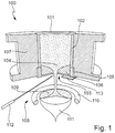
- Fig. 1 shows the schematic representation of a preferred embodiment of a plant 100 according to the invention , which serves for the production of a monocrystalline semiconductor material.
- the plant has the reactor vessel 101 as source for a liquid semiconductor material serving as starting material.
- the reactor vessel shown in section comprises a cylindrical portion bounded laterally by the reactor inner wall 102 .
- the portion of the reactor above the cylindrical portion is not shown, including, inter alia, an inlet for a silicon-containing plasma and an outlet for gases to be discharged from the reactor.
- the plasma is generated in a device upstream of the reactor vessel 101 from a carrier gas and mixed with particles of the semiconductor material and / or a precursor compound of the semiconductor material.
- the interior of the reactor tapers as far as the outlet 103, via which liquid semiconductor material 104 can exit from the reactor vessel 101 .
- this part of the reactor interior is in particular due to the L-shaped cooled wall / floor elements 105 , which adjoin the underside of the reactor inner wall 102 . These are maintained at a temperature below the melting temperature of the semiconductor material contained in the reactor vessel 101 . This forms accordingly a solidified cover layer 106 , which may also extend over the outlet 103 and thus can block the outlet.
- the reactor vessel 101 thus has a bottom region, which at least partially consists of the semiconductor material to be produced.
- Around the reactor inner wall 102 and L-shaped cooled wall / floor elements 105 around the reactor outer wall 107 is arranged. This may include heating, insulating and / or coolant.
- the heating zone 108 is arranged, in which there is a melt 109 of the semiconductor material.
- the heating zone 108 comprises, as heating means, the induction heater 110, which is arranged annularly around the melt 109 .
- the seedling 111 serves as a base. This can be lowered from the heating zone 108 via suitable means together with the melt 109 , so that a solidification front forms at the lower end of the melt 109 , along which the semiconductor material crystallizes in the monocrystalline structure of the end cone 111 .
- the induction heater 110 is used in particular for maintaining the melt 109 in the heating zone 108. Furthermore, it also heats the bottom region of the reactor vessel 101.
- the laser 112 as angordnet means as a means for controlled feeding of the starting material serving as a liquid semiconductor material in the melt 109 such is that it can be focused to the outlet 103, can be the outlet 103 optionally blocking semiconductor material melt so that the melt can be fed with liquid 109 controlled semiconductor material.
- the plant 100 according to the invention as a backup comprises the blocking agent 113, which is a slide, with which the outlet 103 can be closed.
- the slider is preferred made of a material that can not or hardly be heated by high-frequency induction.
Applications Claiming Priority (3)
| Application Number | Priority Date | Filing Date | Title |
|---|---|---|---|
| DE102010015354A DE102010015354A1 (de) | 2010-04-13 | 2010-04-13 | Herstellung eines kristallinen Halbleiterwerkstoffs |
| DE201010021004 DE102010021004A1 (de) | 2010-05-14 | 2010-05-14 | Herstellung von monokristallinen Halbleiterwerkstoffen |
| PCT/EP2011/055626 WO2011128292A1 (de) | 2010-04-13 | 2011-04-11 | Herstellung von monokristallinen halbleiterwerkstoffen |
Publications (2)
| Publication Number | Publication Date |
|---|---|
| EP2558232A1 EP2558232A1 (de) | 2013-02-20 |
| EP2558232B1 true EP2558232B1 (de) | 2017-07-12 |
Family
ID=44009837
Family Applications (1)
| Application Number | Title | Priority Date | Filing Date |
|---|---|---|---|
| EP11714743.9A Active EP2558232B1 (de) | 2010-04-13 | 2011-04-11 | Herstellung von monokristallinen halbleiterwerkstoffen |
Country Status (7)
| Country | Link |
|---|---|
| US (1) | US20130199440A1 (ja) |
| EP (1) | EP2558232B1 (ja) |
| JP (1) | JP5886831B2 (ja) |
| CN (1) | CN102947025B (ja) |
| CA (1) | CA2795395C (ja) |
| TW (1) | TW201200641A (ja) |
| WO (1) | WO2011128292A1 (ja) |
Families Citing this family (10)
| Publication number | Priority date | Publication date | Assignee | Title |
|---|---|---|---|---|
| US20100325565A1 (en) * | 2009-06-17 | 2010-12-23 | EchoStar Technologies, L.L.C. | Apparatus and methods for generating graphical interfaces |
| DE102009052745A1 (de) * | 2009-11-11 | 2011-05-12 | Siltronic Ag | Verfahren zur Herstellung eines Einkristalls aus Silizium durch Umschmelzen von Granulat |
| US9443923B2 (en) * | 2014-05-07 | 2016-09-13 | Raytheon Company | Substrate for molecular beam epitaxy (MBE) HgCdTe growth |
| DE102015215858B4 (de) * | 2015-08-20 | 2019-01-24 | Siltronic Ag | Verfahren zur Wärmebehandlung von Granulat aus Silizium, Granulat aus Silizium und Verfahren zur Herstellung eines Einkristalls aus Silizium |
| CN107779951B (zh) * | 2017-12-17 | 2018-07-17 | 内蒙古赛宝伦科技有限公司 | 硅晶体的连续生长装置 |
| CN107964681B (zh) * | 2017-12-17 | 2019-08-06 | 江苏金晖光伏有限公司 | 硅晶体的连续生长方法 |
| CN108588830B (zh) * | 2018-07-26 | 2019-08-06 | 江苏金晖光伏有限公司 | 提纯太阳能级多晶硅的装置 |
| CN108546987B (zh) * | 2018-07-26 | 2019-08-06 | 江苏金晖光伏有限公司 | 提纯太阳能级多晶硅的方法 |
| CN109056063A (zh) * | 2018-08-29 | 2018-12-21 | 孟静 | 太阳能电池用多晶硅片的制备方法 |
| DE102019211921A1 (de) * | 2019-08-08 | 2021-02-11 | Schmid Silicon Technology Gmbh | Verfahren und Vorrichtung zur Erzeugung siliziumhaltiger Materialien |
Family Cites Families (16)
| Publication number | Priority date | Publication date | Assignee | Title |
|---|---|---|---|---|
| US3658119A (en) * | 1968-04-03 | 1972-04-25 | Airco Inc | Apparatus for processing molten metal in a vacuum |
| US4080172A (en) * | 1975-12-29 | 1978-03-21 | Monsanto Company | Zone refiner automatic control |
| US4102767A (en) * | 1977-04-14 | 1978-07-25 | Westinghouse Electric Corp. | Arc heater method for the production of single crystal silicon |
| US5108720A (en) * | 1991-05-20 | 1992-04-28 | Hemlock Semiconductor Corporation | Float zone processing of particulate silicon |
| JP3053958B2 (ja) * | 1992-04-10 | 2000-06-19 | 光弘 丸山 | 浮遊帯溶融法による結晶の製造装置 |
| DE19538020A1 (de) * | 1995-10-12 | 1997-04-17 | Wacker Siltronic Halbleitermat | Verfahren und Vorrichtung zur Herstellung von Einkristallen aus Silicium |
| JP3325900B2 (ja) * | 1996-10-14 | 2002-09-17 | 川崎製鉄株式会社 | 多結晶シリコンの製造方法及び装置、並びに太陽電池用シリコン基板の製造方法 |
| JP3644227B2 (ja) * | 1997-12-22 | 2005-04-27 | 信越半導体株式会社 | シリコン単結晶の製造方法及び製造装置 |
| JPH11292682A (ja) * | 1998-04-02 | 1999-10-26 | Shin Etsu Handotai Co Ltd | シリコン単結晶の製造方法および製造装置 |
| US6994835B2 (en) * | 2000-12-28 | 2006-02-07 | Sumitomo Mitsubishi Silicon Corporation | Silicon continuous casting method |
| DE10204178B4 (de) * | 2002-02-01 | 2008-01-03 | Siltronic Ag | Verfahren und Vorrichtung zum Herstellen eines Einkristalls aus Halbleitermaterial |
| JP5122128B2 (ja) | 2003-02-11 | 2013-01-16 | トップシル・セミコンダクター・マテリアルズ・アクティーゼルスカブ | 単結晶棒を製造する装置および方法 |
| DE102008013326B4 (de) * | 2008-03-10 | 2013-03-28 | Siltronic Ag | Induktionsheizspule und Verfahren zum Schmelzen von Granulat aus Halbleitermaterial |
| DE102008017304A1 (de) | 2008-03-31 | 2009-10-01 | Schmid Silicon Technology Gmbh | Verfahren und Anlage zur Herstellung von Reinstsilizium |
| US20090289390A1 (en) * | 2008-05-23 | 2009-11-26 | Rec Silicon, Inc. | Direct silicon or reactive metal casting |
| DE102008059408A1 (de) | 2008-11-27 | 2010-06-02 | Schmid Silicon Technology Gmbh | Verfahren und Vorrichtungen zur Herstellung von Reinstsilizium |
-
2011
- 2011-04-11 WO PCT/EP2011/055626 patent/WO2011128292A1/de active Application Filing
- 2011-04-11 CN CN201180019047.7A patent/CN102947025B/zh active Active
- 2011-04-11 US US13/639,170 patent/US20130199440A1/en not_active Abandoned
- 2011-04-11 JP JP2013504221A patent/JP5886831B2/ja not_active Expired - Fee Related
- 2011-04-11 EP EP11714743.9A patent/EP2558232B1/de active Active
- 2011-04-11 CA CA2795395A patent/CA2795395C/en not_active Expired - Fee Related
- 2011-04-13 TW TW100112836A patent/TW201200641A/zh unknown
Non-Patent Citations (1)
| Title |
|---|
| None * |
Also Published As
| Publication number | Publication date |
|---|---|
| CA2795395C (en) | 2018-05-29 |
| CN102947025A (zh) | 2013-02-27 |
| CA2795395A1 (en) | 2011-10-20 |
| TW201200641A (en) | 2012-01-01 |
| CN102947025B (zh) | 2016-04-13 |
| EP2558232A1 (de) | 2013-02-20 |
| JP2013523594A (ja) | 2013-06-17 |
| WO2011128292A1 (de) | 2011-10-20 |
| US20130199440A1 (en) | 2013-08-08 |
| JP5886831B2 (ja) | 2016-03-16 |
Similar Documents
| Publication | Publication Date | Title |
|---|---|---|
| EP2558232B1 (de) | Herstellung von monokristallinen halbleiterwerkstoffen | |
| EP1936012B1 (de) | Verfahren zum Herstellen kristallisierten Siliciums sowie kristallisiertes Silicium | |
| DE102006017622A1 (de) | Verfahren und Vorrichtung zur Herstellung von multikristallinem Silizium | |
| CH670624A5 (ja) | ||
| CH661919A5 (de) | Verfahren und einrichtung zur erzeugung von silizium aus siliciumtetrafluorid. | |
| DE102005044328A1 (de) | Polykristallines Siliziummaterial für die solare Stromerzeugung und Siliziumhalbleiterscheiben für die solare Stromerzeugung | |
| DE112010004412T5 (de) | Verfahren zum reinigen metallurgischen siliziums | |
| DE102011006888A1 (de) | Verfahren und System zum Herstellen von Silizium und Siliziumkarbid | |
| DE102008013543A1 (de) | Vorrichtung und Verfahren zur Herstellung von polykristallinem Silizium mit hoher Reinheit | |
| EP1400490A1 (de) | Abscheidung eines Feststoffs durch thermische Zersetzung einer gasförmigen Substanz in einem Becherreaktor | |
| CH661918A5 (de) | Verfahren und einrichtung zur erzeugung von silizium aus siliciumtetrafluorid. | |
| EP1339638A1 (de) | Verfahren zur herstellung von hochreinem, granularem silizium | |
| DE102008036143A1 (de) | Verfahren zum Entfernen von nichtmetallischen Verunreinigungen aus metallurgischem Silicium | |
| DE102010021004A1 (de) | Herstellung von monokristallinen Halbleiterwerkstoffen | |
| EP2558233B1 (de) | Herstellung eines kristallinen halbleiterwerkstoffs | |
| WO2015113894A1 (de) | Verfahren zur herstellung von polykristallinem silicium | |
| EP3554999A1 (de) | Verfahren zur herstellung von polykristallinem silicium | |
| EP3253908A1 (de) | Verfahren zur herstellung von multikristallinem silicium | |
| DE3138227A1 (de) | Verfahren zur herstellung von silicum-einkristallen | |
| DE102009035041B3 (de) | Anlage zur Herstellung von Silizium-Granulat | |
| DE112017001711B4 (de) | Kristallzüchtungsvorrichtung und diesbezügliche Verfahren | |
| WO2008119331A2 (de) | Carbothermisches reduktionsverfahren und vorrichtung zu dessen durchführung | |
| WO2018108258A1 (de) | Verfahren zur herstellung von polykristallinem silicium | |
| DE112009003720T5 (de) | Verfahren zur Herstellung von Silicium | |
| DE102010045040A1 (de) | Verfahren und Vorrichtung zum Herstellen von Silizium |
Legal Events
| Date | Code | Title | Description |
|---|---|---|---|
| PUAI | Public reference made under article 153(3) epc to a published international application that has entered the european phase |
Free format text: ORIGINAL CODE: 0009012 |
|
| 17P | Request for examination filed |
Effective date: 20121024 |
|
| AK | Designated contracting states |
Kind code of ref document: A1 Designated state(s): AL AT BE BG CH CY CZ DE DK EE ES FI FR GB GR HR HU IE IS IT LI LT LU LV MC MK MT NL NO PL PT RO RS SE SI SK SM TR |
|
| DAX | Request for extension of the european patent (deleted) | ||
| 17Q | First examination report despatched |
Effective date: 20140807 |
|
| GRAP | Despatch of communication of intention to grant a patent |
Free format text: ORIGINAL CODE: EPIDOSNIGR1 |
|
| INTG | Intention to grant announced |
Effective date: 20170228 |
|
| GRAS | Grant fee paid |
Free format text: ORIGINAL CODE: EPIDOSNIGR3 |
|
| GRAA | (expected) grant |
Free format text: ORIGINAL CODE: 0009210 |
|
| AK | Designated contracting states |
Kind code of ref document: B1 Designated state(s): AL AT BE BG CH CY CZ DE DK EE ES FI FR GB GR HR HU IE IS IT LI LT LU LV MC MK MT NL NO PL PT RO RS SE SI SK SM TR |
|
| REG | Reference to a national code |
Ref country code: GB Ref legal event code: FG4D Free format text: NOT ENGLISH |
|
| REG | Reference to a national code |
Ref country code: CH Ref legal event code: EP |
|
| REG | Reference to a national code |
Ref country code: AT Ref legal event code: REF Ref document number: 907860 Country of ref document: AT Kind code of ref document: T Effective date: 20170715 |
|
| REG | Reference to a national code |
Ref country code: IE Ref legal event code: FG4D Free format text: LANGUAGE OF EP DOCUMENT: GERMAN |
|
| REG | Reference to a national code |
Ref country code: DE Ref legal event code: R096 Ref document number: 502011012593 Country of ref document: DE |
|
| REG | Reference to a national code |
Ref country code: NL Ref legal event code: MP Effective date: 20170712 |
|
| REG | Reference to a national code |
Ref country code: LT Ref legal event code: MG4D |
|
| PG25 | Lapsed in a contracting state [announced via postgrant information from national office to epo] |
Ref country code: FI Free format text: LAPSE BECAUSE OF FAILURE TO SUBMIT A TRANSLATION OF THE DESCRIPTION OR TO PAY THE FEE WITHIN THE PRESCRIBED TIME-LIMIT Effective date: 20170712 Ref country code: NL Free format text: LAPSE BECAUSE OF FAILURE TO SUBMIT A TRANSLATION OF THE DESCRIPTION OR TO PAY THE FEE WITHIN THE PRESCRIBED TIME-LIMIT Effective date: 20170712 Ref country code: NO Free format text: LAPSE BECAUSE OF FAILURE TO SUBMIT A TRANSLATION OF THE DESCRIPTION OR TO PAY THE FEE WITHIN THE PRESCRIBED TIME-LIMIT Effective date: 20171012 Ref country code: SE Free format text: LAPSE BECAUSE OF FAILURE TO SUBMIT A TRANSLATION OF THE DESCRIPTION OR TO PAY THE FEE WITHIN THE PRESCRIBED TIME-LIMIT Effective date: 20170712 Ref country code: HR Free format text: LAPSE BECAUSE OF FAILURE TO SUBMIT A TRANSLATION OF THE DESCRIPTION OR TO PAY THE FEE WITHIN THE PRESCRIBED TIME-LIMIT Effective date: 20170712 Ref country code: LT Free format text: LAPSE BECAUSE OF FAILURE TO SUBMIT A TRANSLATION OF THE DESCRIPTION OR TO PAY THE FEE WITHIN THE PRESCRIBED TIME-LIMIT Effective date: 20170712 |
|
| PG25 | Lapsed in a contracting state [announced via postgrant information from national office to epo] |
Ref country code: LV Free format text: LAPSE BECAUSE OF FAILURE TO SUBMIT A TRANSLATION OF THE DESCRIPTION OR TO PAY THE FEE WITHIN THE PRESCRIBED TIME-LIMIT Effective date: 20170712 Ref country code: GR Free format text: LAPSE BECAUSE OF FAILURE TO SUBMIT A TRANSLATION OF THE DESCRIPTION OR TO PAY THE FEE WITHIN THE PRESCRIBED TIME-LIMIT Effective date: 20171013 Ref country code: IS Free format text: LAPSE BECAUSE OF FAILURE TO SUBMIT A TRANSLATION OF THE DESCRIPTION OR TO PAY THE FEE WITHIN THE PRESCRIBED TIME-LIMIT Effective date: 20171112 Ref country code: PL Free format text: LAPSE BECAUSE OF FAILURE TO SUBMIT A TRANSLATION OF THE DESCRIPTION OR TO PAY THE FEE WITHIN THE PRESCRIBED TIME-LIMIT Effective date: 20170712 Ref country code: RS Free format text: LAPSE BECAUSE OF FAILURE TO SUBMIT A TRANSLATION OF THE DESCRIPTION OR TO PAY THE FEE WITHIN THE PRESCRIBED TIME-LIMIT Effective date: 20170712 Ref country code: BG Free format text: LAPSE BECAUSE OF FAILURE TO SUBMIT A TRANSLATION OF THE DESCRIPTION OR TO PAY THE FEE WITHIN THE PRESCRIBED TIME-LIMIT Effective date: 20171012 Ref country code: ES Free format text: LAPSE BECAUSE OF FAILURE TO SUBMIT A TRANSLATION OF THE DESCRIPTION OR TO PAY THE FEE WITHIN THE PRESCRIBED TIME-LIMIT Effective date: 20170712 |
|
| REG | Reference to a national code |
Ref country code: DE Ref legal event code: R097 Ref document number: 502011012593 Country of ref document: DE |
|
| REG | Reference to a national code |
Ref country code: FR Ref legal event code: PLFP Year of fee payment: 8 |
|
| PG25 | Lapsed in a contracting state [announced via postgrant information from national office to epo] |
Ref country code: RO Free format text: LAPSE BECAUSE OF FAILURE TO SUBMIT A TRANSLATION OF THE DESCRIPTION OR TO PAY THE FEE WITHIN THE PRESCRIBED TIME-LIMIT Effective date: 20170712 Ref country code: DK Free format text: LAPSE BECAUSE OF FAILURE TO SUBMIT A TRANSLATION OF THE DESCRIPTION OR TO PAY THE FEE WITHIN THE PRESCRIBED TIME-LIMIT Effective date: 20170712 Ref country code: CZ Free format text: LAPSE BECAUSE OF FAILURE TO SUBMIT A TRANSLATION OF THE DESCRIPTION OR TO PAY THE FEE WITHIN THE PRESCRIBED TIME-LIMIT Effective date: 20170712 |
|
| PLBE | No opposition filed within time limit |
Free format text: ORIGINAL CODE: 0009261 |
|
| STAA | Information on the status of an ep patent application or granted ep patent |
Free format text: STATUS: NO OPPOSITION FILED WITHIN TIME LIMIT |
|
| PG25 | Lapsed in a contracting state [announced via postgrant information from national office to epo] |
Ref country code: SK Free format text: LAPSE BECAUSE OF FAILURE TO SUBMIT A TRANSLATION OF THE DESCRIPTION OR TO PAY THE FEE WITHIN THE PRESCRIBED TIME-LIMIT Effective date: 20170712 Ref country code: EE Free format text: LAPSE BECAUSE OF FAILURE TO SUBMIT A TRANSLATION OF THE DESCRIPTION OR TO PAY THE FEE WITHIN THE PRESCRIBED TIME-LIMIT Effective date: 20170712 Ref country code: SM Free format text: LAPSE BECAUSE OF FAILURE TO SUBMIT A TRANSLATION OF THE DESCRIPTION OR TO PAY THE FEE WITHIN THE PRESCRIBED TIME-LIMIT Effective date: 20170712 |
|
| 26N | No opposition filed |
Effective date: 20180413 |
|
| PG25 | Lapsed in a contracting state [announced via postgrant information from national office to epo] |
Ref country code: SI Free format text: LAPSE BECAUSE OF FAILURE TO SUBMIT A TRANSLATION OF THE DESCRIPTION OR TO PAY THE FEE WITHIN THE PRESCRIBED TIME-LIMIT Effective date: 20170712 |
|
| PG25 | Lapsed in a contracting state [announced via postgrant information from national office to epo] |
Ref country code: MT Free format text: LAPSE BECAUSE OF FAILURE TO SUBMIT A TRANSLATION OF THE DESCRIPTION OR TO PAY THE FEE WITHIN THE PRESCRIBED TIME-LIMIT Effective date: 20170712 |
|
| PG25 | Lapsed in a contracting state [announced via postgrant information from national office to epo] |
Ref country code: MC Free format text: LAPSE BECAUSE OF FAILURE TO SUBMIT A TRANSLATION OF THE DESCRIPTION OR TO PAY THE FEE WITHIN THE PRESCRIBED TIME-LIMIT Effective date: 20170712 |
|
| REG | Reference to a national code |
Ref country code: CH Ref legal event code: PL |
|
| REG | Reference to a national code |
Ref country code: BE Ref legal event code: MM Effective date: 20180430 |
|
| GBPC | Gb: european patent ceased through non-payment of renewal fee |
Effective date: 20180411 |
|
| REG | Reference to a national code |
Ref country code: IE Ref legal event code: MM4A |
|
| PG25 | Lapsed in a contracting state [announced via postgrant information from national office to epo] |
Ref country code: LU Free format text: LAPSE BECAUSE OF NON-PAYMENT OF DUE FEES Effective date: 20180411 |
|
| PG25 | Lapsed in a contracting state [announced via postgrant information from national office to epo] |
Ref country code: GB Free format text: LAPSE BECAUSE OF NON-PAYMENT OF DUE FEES Effective date: 20180411 Ref country code: BE Free format text: LAPSE BECAUSE OF NON-PAYMENT OF DUE FEES Effective date: 20180430 Ref country code: CH Free format text: LAPSE BECAUSE OF NON-PAYMENT OF DUE FEES Effective date: 20180430 Ref country code: LI Free format text: LAPSE BECAUSE OF NON-PAYMENT OF DUE FEES Effective date: 20180430 |
|
| PG25 | Lapsed in a contracting state [announced via postgrant information from national office to epo] |
Ref country code: IE Free format text: LAPSE BECAUSE OF NON-PAYMENT OF DUE FEES Effective date: 20180411 |
|
| REG | Reference to a national code |
Ref country code: AT Ref legal event code: MM01 Ref document number: 907860 Country of ref document: AT Kind code of ref document: T Effective date: 20180411 |
|
| PG25 | Lapsed in a contracting state [announced via postgrant information from national office to epo] |
Ref country code: AT Free format text: LAPSE BECAUSE OF NON-PAYMENT OF DUE FEES Effective date: 20180411 |
|
| PG25 | Lapsed in a contracting state [announced via postgrant information from national office to epo] |
Ref country code: HU Free format text: LAPSE BECAUSE OF FAILURE TO SUBMIT A TRANSLATION OF THE DESCRIPTION OR TO PAY THE FEE WITHIN THE PRESCRIBED TIME-LIMIT; INVALID AB INITIO Effective date: 20110411 Ref country code: PT Free format text: LAPSE BECAUSE OF FAILURE TO SUBMIT A TRANSLATION OF THE DESCRIPTION OR TO PAY THE FEE WITHIN THE PRESCRIBED TIME-LIMIT Effective date: 20170712 |
|
| PG25 | Lapsed in a contracting state [announced via postgrant information from national office to epo] |
Ref country code: CY Free format text: LAPSE BECAUSE OF FAILURE TO SUBMIT A TRANSLATION OF THE DESCRIPTION OR TO PAY THE FEE WITHIN THE PRESCRIBED TIME-LIMIT Effective date: 20170712 Ref country code: MK Free format text: LAPSE BECAUSE OF NON-PAYMENT OF DUE FEES Effective date: 20170712 |
|
| PG25 | Lapsed in a contracting state [announced via postgrant information from national office to epo] |
Ref country code: AL Free format text: LAPSE BECAUSE OF FAILURE TO SUBMIT A TRANSLATION OF THE DESCRIPTION OR TO PAY THE FEE WITHIN THE PRESCRIBED TIME-LIMIT Effective date: 20170712 |
|
| PGFP | Annual fee paid to national office [announced via postgrant information from national office to epo] |
Ref country code: FR Payment date: 20200421 Year of fee payment: 10 Ref country code: TR Payment date: 20200508 Year of fee payment: 10 |
|
| PGFP | Annual fee paid to national office [announced via postgrant information from national office to epo] |
Ref country code: IT Payment date: 20200423 Year of fee payment: 10 |
|
| REG | Reference to a national code |
Ref country code: DE Ref legal event code: R082 Ref document number: 502011012593 Country of ref document: DE Representative=s name: OSTERTAG & PARTNER, PATENTANWAELTE MBB, DE |
|
| PG25 | Lapsed in a contracting state [announced via postgrant information from national office to epo] |
Ref country code: FR Free format text: LAPSE BECAUSE OF NON-PAYMENT OF DUE FEES Effective date: 20210430 |
|
| PG25 | Lapsed in a contracting state [announced via postgrant information from national office to epo] |
Ref country code: IT Free format text: LAPSE BECAUSE OF NON-PAYMENT OF DUE FEES Effective date: 20200411 |
|
| P01 | Opt-out of the competence of the unified patent court (upc) registered |
Effective date: 20230526 |
|
| PGFP | Annual fee paid to national office [announced via postgrant information from national office to epo] |
Ref country code: DE Payment date: 20230420 Year of fee payment: 13 |