EP2555006A2 - Semiconductor device - Google Patents
Semiconductor device Download PDFInfo
- Publication number
- EP2555006A2 EP2555006A2 EP12157652A EP12157652A EP2555006A2 EP 2555006 A2 EP2555006 A2 EP 2555006A2 EP 12157652 A EP12157652 A EP 12157652A EP 12157652 A EP12157652 A EP 12157652A EP 2555006 A2 EP2555006 A2 EP 2555006A2
- Authority
- EP
- European Patent Office
- Prior art keywords
- pad
- semiconductor device
- electrically connected
- test
- semiconductor
- Prior art date
- Legal status (The legal status is an assumption and is not a legal conclusion. Google has not performed a legal analysis and makes no representation as to the accuracy of the status listed.)
- Granted
Links
Images

Classifications
-
- H—ELECTRICITY
- H05—ELECTRIC TECHNIQUES NOT OTHERWISE PROVIDED FOR
- H05K—PRINTED CIRCUITS; CASINGS OR CONSTRUCTIONAL DETAILS OF ELECTRIC APPARATUS; MANUFACTURE OF ASSEMBLAGES OF ELECTRICAL COMPONENTS
- H05K1/00—Printed circuits
- H05K1/18—Printed circuits structurally associated with non-printed electric components
-
- G—PHYSICS
- G01—MEASURING; TESTING
- G01R—MEASURING ELECTRIC VARIABLES; MEASURING MAGNETIC VARIABLES
- G01R31/00—Arrangements for testing electric properties; Arrangements for locating electric faults; Arrangements for electrical testing characterised by what is being tested not provided for elsewhere
- G01R31/50—Testing of electric apparatus, lines, cables or components for short-circuits, continuity, leakage current or incorrect line connections
- G01R31/66—Testing of connections, e.g. of plugs or non-disconnectable joints
- G01R31/70—Testing of connections between components and printed circuit boards
-
- H—ELECTRICITY
- H05—ELECTRIC TECHNIQUES NOT OTHERWISE PROVIDED FOR
- H05K—PRINTED CIRCUITS; CASINGS OR CONSTRUCTIONAL DETAILS OF ELECTRIC APPARATUS; MANUFACTURE OF ASSEMBLAGES OF ELECTRICAL COMPONENTS
- H05K3/00—Apparatus or processes for manufacturing printed circuits
- H05K3/30—Assembling printed circuits with electric components, e.g. with resistors
- H05K3/32—Assembling printed circuits with electric components, e.g. with resistors electrically connecting electric components or wires to printed circuits
- H05K3/34—Assembling printed circuits with electric components, e.g. with resistors electrically connecting electric components or wires to printed circuits by soldering
-
- H—ELECTRICITY
- H10—SEMICONDUCTOR DEVICES; ELECTRIC SOLID-STATE DEVICES NOT OTHERWISE PROVIDED FOR
- H10W—GENERIC PACKAGES, INTERCONNECTIONS, CONNECTORS OR OTHER CONSTRUCTIONAL DETAILS OF DEVICES COVERED BY CLASS H10
- H10W70/00—Package substrates; Interposers; Redistribution layers [RDL]
- H10W70/60—Insulating or insulated package substrates; Interposers; Redistribution layers
-
- H—ELECTRICITY
- H10—SEMICONDUCTOR DEVICES; ELECTRIC SOLID-STATE DEVICES NOT OTHERWISE PROVIDED FOR
- H10W—GENERIC PACKAGES, INTERCONNECTIONS, CONNECTORS OR OTHER CONSTRUCTIONAL DETAILS OF DEVICES COVERED BY CLASS H10
- H10W90/00—Package configurations
- H10W90/701—Package configurations characterised by the relative positions of pads or connectors relative to package parts
- H10W90/751—Package configurations characterised by the relative positions of pads or connectors relative to package parts of bond wires
- H10W90/756—Package configurations characterised by the relative positions of pads or connectors relative to package parts of bond wires between a chip and a stacked lead frame, conducting package substrate or heat sink
Definitions
- Exemplary embodiments of the present invention relate to a semiconductor device. More particularly, exemplary embodiments of the present invention relate to a semiconductor package disposed on a circuit board.
- a semiconductor package protects a semiconductor chip from an external environment, and controls the humidity and temperature of the area surrounding the semiconductor chip. Advancements in semiconductor packaging technology have resulted in semiconductor packages that are light, thin, small, and have a high density.
- a semiconductor package may be classified as an inserting-type package or a surface-mounting-type package.
- a quad flat pack (QFP) semiconductor package is a type of surface-mounting package that is often used for a timing controller in a liquid crystal display.
- the package used for the timing controller may include an exposed pad at the rear surface of the package.
- the exposed pad may be bonded to a ground surface on a circuit board, so as to stably maintain a ground level of the semiconductor chip and discharge heat to the rear surface.
- Exemplary embodiments of the present invention include a semiconductor device that allows for a determination to be made regarding whether an exposed pad of a semiconductor package is firmly bonded with a ground surface of a circuit board.
- An exemplary embodiment of the present invention includes a semiconductor device including a circuit board including a ground portion, a semiconductor package disposed on the circuit board and including an external connecting pad and an exposed pad, a semiconductor chip disposed on the exposed pad and electrically connected to the external connecting pad, and a test pad disposed on the semiconductor chip and electrically connected to the exposed pad.
- the exposed pad and the ground portion of the circuit board are electrically connected at a first surface of the exposed pad.
- the semiconductor chip is disposed on a second surface of the exposed pad. The first surface of the exposed pad is located external to the semiconductor package and the second surface of the exposed pad is located within the semiconductor package.
- the semiconductor device may include a resistor part disposed in the semiconductor chip, and electrically connected to the test pad.
- the resistor part may be a pull-up resistor.
- the semiconductor device may be configured to output a logic high signal when the semiconductor device is operating in a fail mode, and output a logic low signal when the semiconductor device is operating in a normal mode.
- the semiconductor device may operate in the fail mode when the exposed pad and the ground portion are not electrically connected, and operate in the normal mode when the exposed pad and the ground portion are electrically connected.
- the first portion of the resistor part may be connected to a voltage source, and a second portion of the resistor part may be connected to the test pad.
- the semiconductor device may include a wire electrically connecting the test pad and the exposed pad.
- the semiconductor device may include a test pin electrically connected to the test pad, and a test point disposed in the semiconductor package and electrically connected to the test pin.
- the test point may be an end of the test pin.
- the test point may be an electrical pad, and the test pin may be electrically connected to the electrical pad.
- the semiconductor device may include a measuring device electrically connected to the test point, and configured to determine whether the exposed pad and the ground portion are electrically connected.
- the external connecting pad may be disposed substantially near a first corner of the semiconductor package, and the test point may be disposed substantially near a second, opposing corner of the semiconductor package.
- the test pad may be disposed near an edge of an upper surface of the semiconductor chip.
- the exposed pad and the ground portion of the circuit board may be bonded to each other using solder.
- the semiconductor device may include a wire electrically connecting the semiconductor chip and the external connecting pad.
- An exemplary embodiment of the present invention includes a semiconductor package including an external connecting pad, an exposed pad having a first surface and a second surface, a semiconductor chip, and a test pad.
- the first surface of the exposed pad is located external to the semiconductor package and is electrically connected to a ground portion of a circuit board.
- the second surface is located within the semiconductor package.
- the semiconductor chip is disposed on the second surface of the exposed pad, and is electrically connected to the external connecting pad.
- the test pad is disposed on the semiconductor chip, and is electrically connected to the exposed pad.
- the semiconductor package may include a resistor part disposed in the semiconductor chip, and electrically connected to the test pad.
- the resistor part may be a pull-up resistor.
- the semiconductor package may be configured to output a logic high signal when the semiconductor package is operating in a fail mode, and output a logic low signal when the semiconductor package is operating in a normal mode.
- the semiconductor package may include a test pin electrically connected to the test pad, and a test point disposed in the semiconductor package and electrically connected to the test pin.
- a contact defect(s) present between the ground surface of the circuit board and the exposed pad of the semiconductor package may be detected without using an additional pin.
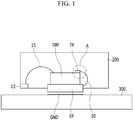
- FIG 1 is a cross-sectional view illustrating a semiconductor device according to an exemplary embodiment of the present invention.
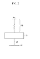
- FIG 2 is an enlarged schematic view illustrating portion "A" of FIG 1 .
- a semiconductor package 200 is disposed on a circuit board 300.
- An exposed pad (e.g., e-pad EP) is disposed at the rear surface of the semiconductor package 200.
- the e-pad EP is located near the center of the rear surface of the semiconductor package 200, however, the location of the e-pad EP is not limited thereto.
- a semiconductor chip 100 is disposed on the e-pad EP.
- the semiconductor chip 100 is connected to an external connecting pad 13.
- wire bonding using wiring 15 may be utilized to electrically connect the semiconductor chip 100 to the external connecting pad 13.
- the external connecting pad 13 is disposed near a corner of the semiconductor package, however, the location of the external connecting pad 13 is not limited thereto.
- a test pad TP is disposed on the semiconductor chip 100.
- the test pad TP may be disposed at a variety of locations on the semiconductor chip 100.
- the test pad TP is disposed near an edge of the upper surface of the semiconductor chip 100, and the test pad TP is electrically connected to the e-pad EP.
- Wire bonding using wiring 20 may be used to electrically connect the test pad TP and the e-pad EP, as shown in FIG 1 , however the manner in which the test pad TP and the e-pad EP are electrically connected is not limited thereto.
- the circuit board 300 includes a ground surface GND disposed at a portion corresponding to the e-pad EP of the semiconductor package 200.
- the ground surface GND is disposed near the center of the circuit board 300 such that the ground surface GND aligns with the e-pad EP of the semiconductor package 200.
- the ground surface GND and the e-pad EP may be disposed at a variety of locations on the circuit board 300 and the semiconductor package 200, respectively.
- a space is shown between the ground surface GND of the circuit board 300 and the e-pad EP. As will be appreciated by one having ordinary skill in the art, this space is included for illustrative purposes to show the formation and alignment of the ground surface GND and the e-pad EP.
- the ground surface GND of the circuit board 300 and the e-pad EP make contact with each other.
- the e-pad EP includes a first surface and a second, opposing surface. As shown in FIG 1 , the first surface of the e-pad EP is located external to the semiconductor package 200, and makes contact with the ground surface GND of the circuit board 300.
- the second surface of the e-pad EP is located within the semiconductor package 200, and may be connected to the semiconductor chip 100.
- FIG 2 is an enlarged schematic view illustrating portion "A" of FIG 1 .
- the test pad TP is connected to a resistor part RP.
- the resistor part RP may be an element disposed in the semiconductor chip 100 having a resistance.
- the resistor part RP may be a pull-up resistor.
- the e-pad EP and the ground surface GND are in contact with each other.
- the e-pad EP and the ground surface GND may be bonded to each other using a soldering process to maintain contact.
- Contact defects may be generated during the soldering process, resulting in a break in the connection between the e-pad EP and the ground surface GND.
- the resistor part RP e.g., the pull-up resistor
- the resistor part RP pulls the voltage at the test pad TP towards voltage source Vcc.
- the output of the semiconductor device is brought to a high logic level.
- the semiconductor device is operating in a fail mode.
- the output of the semiconductor device is brought to a low logic level.
- the semiconductor device is operating in a normal mode. Accordingly, exemplary embodiments of the present invention allow for the verification of whether the e-pad EP and the ground surface GND are stably electrically connected with each other (e.g., no contact defects were generated during the soldering process).
- FIG 3 is a cross-sectional view illustrating a semiconductor device according to an exemplary embodiment of the present invention.
- a semiconductor package 200 is disposed on a circuit board 300.
- An exposed pad (e.g., e-pad EP) is disposed at the rear surface of the semiconductor package 200.
- the e-pad EP is located near the center of the rear surface of the semiconductor package 200, however the location of the e-pad EP is not limited thereto.
- a semiconductor chip 100 is disposed on the e-pad EP.
- the semiconductor chip 100 is connected to an external connecting pad 13.
- wire bonding using wiring 15 may be utilized to electrically connect the semiconductor chip 100 to the external connecting pad 13.
- the external connecting pad 13 is disposed near a corner of the semiconductor package 200, however, the location of the external connecting pad 13 is not limited thereto.
- a test pad TP is disposed on the semiconductor chip 100.
- the test pad TP may be disposed at a variety of locations on the semiconductor chip 100.
- the test pad TP is disposed near an edge of the upper surface of the semiconductor chip 100, and the test pad TP is electrically connected to the e-pad EP.
- Wire bonding using wiring 20 may be used to electrically connect the test pad TP and the e-pad EP, as shown in FIG 1 , however the manner in which the test pad TP and the e-pad EP are electrically connected is not limited thereto.
- the circuit board 300 includes a ground surface GND disposed at a portion corresponding to the e-pad EP of the semiconductor package 200.
- the ground surface GND is disposed near the center of the circuit board 300 such that the ground surface GND aligns with the e-pad EP of the semiconductor package 200.
- the ground surface GND and the e-pad EP may be disposed at a variety of locations on the circuit board 300 and the semiconductor package 200, respectively.
- a space is shown between the ground surface GND of the circuit board 300 and the e-pad EP. As will be appreciated by one having ordinary skill in the art, this space is included for illustrative purposes to show the formation and alignment of the ground surface GND and the e-pad EP.
- the ground surface GND of the circuit board 300 and the e-pad EP make contact with each other.
- the e-pad EP includes a first surface and a second, opposing surface. As shown in FIG 3 , the first surface of the e-pad EP is located external to the semiconductor package 200, and makes contact with the ground surface GND of the circuit board 300.
- the second surface of the e-pad EP is located within the semiconductor package 200, and is electrically connected to the semiconductor chip 100.
- the test pad TP is electrically connected to the e-pad EP via wiring 20, and is also connected to test pin 17.
- the test pad TP may also be connected to resistor part RP, as discussed with reference to FIG 2 .
- Test pin 17 extends from the test pad TP of the semiconductor chip 100, and is electrically connected to a test point TPP formed in the semiconductor package 200.
- the test point TPP may be an electrical pad similar to the external connecting pad 13, or an end of the test pin 17 may form the test point TPP.
- the test point TPP is disposed near a corner of the semiconductor package 200, opposite the external connecting pad 13. However, the location of the test point TPP is not limited thereto.
- Measuring equipment may be connected to the test point TPP. The measuring equipment may be used to determine whether the e-pad EP and the ground surface GND are stably electrically connected (e.g., determine whether contact defects were generated during the soldering process).
- the semiconductor chip 100 is electrically connected to an external device via wiring and an external connecting terminal.
- the semiconductor chip 100 receives power and signals from the external device, and outputs the operating result to the external device.
- an operating result having a high logic value indicates that the semiconductor device is operating in a fail mode
- an operating result having a low logic value indicates that the semiconductor device is operating in a normal mode.
- a determination of whether the ground surface of the circuit board 300 and the exposed pad EP of the semiconductor package 200 are properly bonded may be made.
Landscapes
- Engineering & Computer Science (AREA)
- Physics & Mathematics (AREA)
- General Physics & Mathematics (AREA)
- Microelectronics & Electronic Packaging (AREA)
- Manufacturing & Machinery (AREA)
- Tests Of Electronic Circuits (AREA)
- Semiconductor Integrated Circuits (AREA)
- Printing Elements For Providing Electric Connections Between Printed Circuits (AREA)
- Lead Frames For Integrated Circuits (AREA)
- Structure Of Printed Boards (AREA)
Abstract
Description
- Exemplary embodiments of the present invention relate to a semiconductor device. More particularly, exemplary embodiments of the present invention relate to a semiconductor package disposed on a circuit board.
- A semiconductor package protects a semiconductor chip from an external environment, and controls the humidity and temperature of the area surrounding the semiconductor chip. Advancements in semiconductor packaging technology have resulted in semiconductor packages that are light, thin, small, and have a high density. A semiconductor package may be classified as an inserting-type package or a surface-mounting-type package.
- For example, a quad flat pack (QFP) semiconductor package is a type of surface-mounting package that is often used for a timing controller in a liquid crystal display. The package used for the timing controller may include an exposed pad at the rear surface of the package. The exposed pad may be bonded to a ground surface on a circuit board, so as to stably maintain a ground level of the semiconductor chip and discharge heat to the rear surface.
- However, if the exposed pad is not firmly bonded to the ground surface of the circuit board, normal operation of the semiconductor device may not occur due to the insufficient grounding of the timing controller.
- Exemplary embodiments of the present invention include a semiconductor device that allows for a determination to be made regarding whether an exposed pad of a semiconductor package is firmly bonded with a ground surface of a circuit board.
- An exemplary embodiment of the present invention includes a semiconductor device including a circuit board including a ground portion, a semiconductor package disposed on the circuit board and including an external connecting pad and an exposed pad, a semiconductor chip disposed on the exposed pad and electrically connected to the external connecting pad, and a test pad disposed on the semiconductor chip and electrically connected to the exposed pad. The exposed pad and the ground portion of the circuit board are electrically connected at a first surface of the exposed pad. The semiconductor chip is disposed on a second surface of the exposed pad. The first surface of the exposed pad is located external to the semiconductor package and the second surface of the exposed pad is located within the semiconductor package.
- The semiconductor device may include a resistor part disposed in the semiconductor chip, and electrically connected to the test pad.
- The resistor part may be a pull-up resistor.
- The semiconductor device may be configured to output a logic high signal when the semiconductor device is operating in a fail mode, and output a logic low signal when the semiconductor device is operating in a normal mode.
- The semiconductor device may operate in the fail mode when the exposed pad and the ground portion are not electrically connected, and operate in the normal mode when the exposed pad and the ground portion are electrically connected.
- The first portion of the resistor part may be connected to a voltage source, and a second portion of the resistor part may be connected to the test pad.
- The semiconductor device may include a wire electrically connecting the test pad and the exposed pad.
- The semiconductor device may include a test pin electrically connected to the test pad, and a test point disposed in the semiconductor package and electrically connected to the test pin.
- The test point may be an end of the test pin.
- The test point may be an electrical pad, and the test pin may be electrically connected to the electrical pad.
- The semiconductor device may include a measuring device electrically connected to the test point, and configured to determine whether the exposed pad and the ground portion are electrically connected.
- The external connecting pad may be disposed substantially near a first corner of the semiconductor package, and the test point may be disposed substantially near a second, opposing corner of the semiconductor package.
- The test pad may be disposed near an edge of an upper surface of the semiconductor chip.
- The exposed pad and the ground portion of the circuit board may be bonded to each other using solder.
- The semiconductor device may include a wire electrically connecting the semiconductor chip and the external connecting pad.
- An exemplary embodiment of the present invention includes a semiconductor package including an external connecting pad, an exposed pad having a first surface and a second surface, a semiconductor chip, and a test pad. The first surface of the exposed pad is located external to the semiconductor package and is electrically connected to a ground portion of a circuit board. The second surface is located within the semiconductor package. The semiconductor chip is disposed on the second surface of the exposed pad, and is electrically connected to the external connecting pad. The test pad is disposed on the semiconductor chip, and is electrically connected to the exposed pad.
- The semiconductor package may include a resistor part disposed in the semiconductor chip, and electrically connected to the test pad.
- The resistor part may be a pull-up resistor.
- The semiconductor package may be configured to output a logic high signal when the semiconductor package is operating in a fail mode, and output a logic low signal when the semiconductor package is operating in a normal mode.
- The semiconductor package may include a test pin electrically connected to the test pad, and a test point disposed in the semiconductor package and electrically connected to the test pin.
- According to exemplary embodiments of the present invention, a contact defect(s) present between the ground surface of the circuit board and the exposed pad of the semiconductor package may be detected without using an additional pin.
-
-
FIG 1 is a cross-sectional view illustrating a semiconductor device according to an exemplary embodiment of the present invention. -
FIG 2 is an enlarged schematic view illustrating portion "A" ofFIG 1 . -
FIG 3 is a cross-sectional view illustrating a semiconductor device according to an exemplary embodiment of the present invention. - Exemplary embodiments of the present invention will be described more fully hereinafter with reference to the accompanying drawings. As will be understood by those having ordinary skill in the art, the exemplary embodiments may be modified in various ways without departing from the spirit or scope of the present invention. In the drawings, the thickness of layers, films, panels, regions, etc., may be exaggerated for clarity. It will be understood that when a layer is referred to as being "on" another layer or substrate, it may be directly on the other layer or substrate, or an intervening layer or layers may be present. Like reference numerals may refer to like elements throughout the accompanying drawings.
-
FIG 1 is a cross-sectional view illustrating a semiconductor device according to an exemplary embodiment of the present invention.FIG 2 is an enlarged schematic view illustrating portion "A" ofFIG 1 . - Referring to
FIG 1 , asemiconductor package 200 is disposed on acircuit board 300. - An exposed pad (e.g., e-pad EP) is disposed at the rear surface of the
semiconductor package 200. InFIG 1 , the e-pad EP is located near the center of the rear surface of thesemiconductor package 200, however, the location of the e-pad EP is not limited thereto. Asemiconductor chip 100 is disposed on the e-pad EP. Thesemiconductor chip 100 is connected to anexternal connecting pad 13. For example, wirebonding using wiring 15 may be utilized to electrically connect thesemiconductor chip 100 to theexternal connecting pad 13. InFIG 1 , theexternal connecting pad 13 is disposed near a corner of the semiconductor package, however, the location of the external connectingpad 13 is not limited thereto. - According to the exemplary embodiment shown in
FIG 1 , a test pad TP is disposed on thesemiconductor chip 100. The test pad TP may be disposed at a variety of locations on thesemiconductor chip 100. For example, inFIG 1 , the test pad TP is disposed near an edge of the upper surface of thesemiconductor chip 100, and the test pad TP is electrically connected to the e-pad EP. Wirebonding using wiring 20 may be used to electrically connect the test pad TP and the e-pad EP, as shown inFIG 1 , however the manner in which the test pad TP and the e-pad EP are electrically connected is not limited thereto. - The
circuit board 300 includes a ground surface GND disposed at a portion corresponding to the e-pad EP of thesemiconductor package 200. For example, inFIG 1 , the ground surface GND is disposed near the center of thecircuit board 300 such that the ground surface GND aligns with the e-pad EP of thesemiconductor package 200. The ground surface GND and the e-pad EP may be disposed at a variety of locations on thecircuit board 300 and thesemiconductor package 200, respectively. InFIG 1 , a space is shown between the ground surface GND of thecircuit board 300 and the e-pad EP. As will be appreciated by one having ordinary skill in the art, this space is included for illustrative purposes to show the formation and alignment of the ground surface GND and the e-pad EP. In the exemplary embodiment, the ground surface GND of thecircuit board 300 and the e-pad EP make contact with each other. The e-pad EP includes a first surface and a second, opposing surface. As shown inFIG 1 , the first surface of the e-pad EP is located external to thesemiconductor package 200, and makes contact with the ground surface GND of thecircuit board 300. The second surface of the e-pad EP is located within thesemiconductor package 200, and may be connected to thesemiconductor chip 100. -
FIG 2 is an enlarged schematic view illustrating portion "A" ofFIG 1 . - Referring to
FIG 2 , the test pad TP is connected to a resistor part RP. The resistor part RP may be an element disposed in thesemiconductor chip 100 having a resistance. For example, the resistor part RP may be a pull-up resistor. - As discussed above, the e-pad EP and the ground surface GND are in contact with each other. For example, the e-pad EP and the ground surface GND may be bonded to each other using a soldering process to maintain contact. Contact defects may be generated during the soldering process, resulting in a break in the connection between the e-pad EP and the ground surface GND. The resistor part RP (e.g., the pull-up resistor) may be used to determine whether a contact defect has been generated and whether a break in the connection between the e-pad EP and the ground surface GND has occurred.
- For example, when there is a break in the connection between the e-pad EP and the ground surface GND (e.g., a break in the connection may occur when contact defects are generated during the soldering process), the resistor part RP pulls the voltage at the test pad TP towards voltage source Vcc. As a result, the output of the semiconductor device is brought to a high logic level. When the output is a high logic level, the semiconductor device is operating in a fail mode. When the e-pad EP and the ground surface GND are properly connected with each other (e.g., no contact defects were generated during the soldering process), the output of the semiconductor device is brought to a low logic level. When the output is a low logic level, the semiconductor device is operating in a normal mode. Accordingly, exemplary embodiments of the present invention allow for the verification of whether the e-pad EP and the ground surface GND are stably electrically connected with each other (e.g., no contact defects were generated during the soldering process).
-
FIG 3 is a cross-sectional view illustrating a semiconductor device according to an exemplary embodiment of the present invention. - Referring to
FIG 3 , asemiconductor package 200 is disposed on acircuit board 300. - An exposed pad (e.g., e-pad EP) is disposed at the rear surface of the
semiconductor package 200. InFIG 3 , the e-pad EP is located near the center of the rear surface of thesemiconductor package 200, however the location of the e-pad EP is not limited thereto. Asemiconductor chip 100 is disposed on the e-pad EP. Thesemiconductor chip 100 is connected to an external connectingpad 13. For example, wirebonding using wiring 15 may be utilized to electrically connect thesemiconductor chip 100 to the external connectingpad 13. InFIG 3 , the external connectingpad 13 is disposed near a corner of thesemiconductor package 200, however, the location of the external connectingpad 13 is not limited thereto. - According to the exemplary embodiment shown in
FIG 3 , a test pad TP is disposed on thesemiconductor chip 100. The test pad TP may be disposed at a variety of locations on thesemiconductor chip 100. For example, inFIG 3 , the test pad TP is disposed near an edge of the upper surface of thesemiconductor chip 100, and the test pad TP is electrically connected to the e-pad EP. Wirebonding using wiring 20 may be used to electrically connect the test pad TP and the e-pad EP, as shown inFIG 1 , however the manner in which the test pad TP and the e-pad EP are electrically connected is not limited thereto. - The
circuit board 300 includes a ground surface GND disposed at a portion corresponding to the e-pad EP of thesemiconductor package 200. For example, inFIG 3 , the ground surface GND is disposed near the center of thecircuit board 300 such that the ground surface GND aligns with the e-pad EP of thesemiconductor package 200. The ground surface GND and the e-pad EP may be disposed at a variety of locations on thecircuit board 300 and thesemiconductor package 200, respectively. InFIG 3 , a space is shown between the ground surface GND of thecircuit board 300 and the e-pad EP. As will be appreciated by one having ordinary skill in the art, this space is included for illustrative purposes to show the formation and alignment of the ground surface GND and the e-pad EP. In the exemplary embodiment, the ground surface GND of thecircuit board 300 and the e-pad EP make contact with each other. The e-pad EP includes a first surface and a second, opposing surface. As shown inFIG 3 , the first surface of the e-pad EP is located external to thesemiconductor package 200, and makes contact with the ground surface GND of thecircuit board 300. The second surface of the e-pad EP is located within thesemiconductor package 200, and is electrically connected to thesemiconductor chip 100. - In the exemplary embodiment shown in
FIG 3 , the test pad TP is electrically connected to the e-pad EP viawiring 20, and is also connected to testpin 17. The test pad TP may also be connected to resistor part RP, as discussed with reference toFIG 2 .Test pin 17 extends from the test pad TP of thesemiconductor chip 100, and is electrically connected to a test point TPP formed in thesemiconductor package 200. The test point TPP may be an electrical pad similar to the external connectingpad 13, or an end of thetest pin 17 may form the test point TPP. InFIG 3 , the test point TPP is disposed near a corner of thesemiconductor package 200, opposite the external connectingpad 13. However, the location of the test point TPP is not limited thereto. Measuring equipment may be connected to the test point TPP. The measuring equipment may be used to determine whether the e-pad EP and the ground surface GND are stably electrically connected (e.g., determine whether contact defects were generated during the soldering process). - In an exemplary embodiment, the
semiconductor chip 100 is electrically connected to an external device via wiring and an external connecting terminal. Thesemiconductor chip 100 receives power and signals from the external device, and outputs the operating result to the external device. As discussed above, an operating result having a high logic value indicates that the semiconductor device is operating in a fail mode, and an operating result having a low logic value indicates that the semiconductor device is operating in a normal mode. According to exemplary embodiments of the present invention, a determination of whether the ground surface of thecircuit board 300 and the exposed pad EP of thesemiconductor package 200 are properly bonded may be made. - While the present invention has been particularly shown and described with reference to the exemplary embodiments thereof, it will be understood by those having ordinary skill in the art that various changes in form and detail may be made therein without departing from the spirit and scope of the present invention as defined by the following claims.
Claims (15)
- A semiconductor device, comprising:a circuit board comprising a ground portion;a semiconductor package disposed on the circuit board, and comprising an external connecting pad and an exposed pad, wherein the exposed pad and the ground portion are electrically connected at a first surface of the exposed pad;a semiconductor chip disposed on a second surface of the exposed pad and electrically connected to the external connecting pad, wherein the first surface of the exposed pad is located external to the semiconductor package and the second surface of the exposed pad is located within the semiconductor package; anda test pad disposed on the semiconductor chip, and electrically connected to the exposed pad.
- The semiconductor device of claim 1, further comprising:a resistor part disposed in the semiconductor chip, and electrically connected to the test pad.
- The semiconductor device of claim 2, wherein the resistor part comprises a pull-up resistor.
- The semiconductor device of claim 3, wherein the semiconductor device is configured to output a logic high signal when the semiconductor device is operating in a fail mode, and output a logic low signal when the semiconductor device is operating in a normal mode.
- The semiconductor device of claim 4, wherein the semiconductor device operates in the fail mode when the exposed pad and the ground portion are not stably electrically connected, and operates in the normal mode when the exposed pad and the ground portion are stably electrically connected.
- The semiconductor device of claim 2, wherein a first portion of the resistor part is connected to a voltage source and a second portion of the resistor part is connected to the test pad.
- The semiconductor device of claim 1, further comprising:a wire electrically connecting the test pad and the exposed pad.
- The semiconductor device of claim 1, further comprising:a test pin electrically connected to the test pad; anda test point disposed in the semiconductor package and electrically connected to the test pin.
- The semiconductor device of claim 8, wherein the test point comprises an end of the test pin.
- The semiconductor device of claim 8, wherein the test point comprises an electrical pad, and the test pin is electrically connected to the electrical pad.
- The semiconductor device of claim 8, further comprising:a measuring device electrically connected to the test point, and configured to determine whether the exposed pad and the ground portion are electrically connected.
- The semiconductor device of claim 8, wherein the external connecting pad is disposed substantially near a first corner of the semiconductor package, and the test point is disposed substantially near a second, opposing corner of the semiconductor package.
- The semiconductor device of claim 1, wherein the test pad is disposed near an edge of an upper surface of the semiconductor chip.
- The semiconductor device of claim 1, wherein the exposed pad and the ground portion of the circuit board are bonded to each other using solder.
- The semiconductor device of claim 1, further comprising:a wire electrically connecting the semiconductor chip and the external connecting pad.
Applications Claiming Priority (1)
| Application Number | Priority Date | Filing Date | Title |
|---|---|---|---|
| KR1020110077020A KR101912843B1 (en) | 2011-08-02 | 2011-08-02 | Printed circuit board |
Publications (3)
| Publication Number | Publication Date |
|---|---|
| EP2555006A2 true EP2555006A2 (en) | 2013-02-06 |
| EP2555006A3 EP2555006A3 (en) | 2014-12-10 |
| EP2555006B1 EP2555006B1 (en) | 2016-07-27 |
Family
ID=45977139
Family Applications (1)
| Application Number | Title | Priority Date | Filing Date |
|---|---|---|---|
| EP12157652.4A Active EP2555006B1 (en) | 2011-08-02 | 2012-03-01 | Semiconductor device |
Country Status (3)
| Country | Link |
|---|---|
| US (1) | US8963150B2 (en) |
| EP (1) | EP2555006B1 (en) |
| KR (1) | KR101912843B1 (en) |
Families Citing this family (2)
| Publication number | Priority date | Publication date | Assignee | Title |
|---|---|---|---|---|
| US10734296B2 (en) | 2018-12-28 | 2020-08-04 | Micron Technology, Inc. | Electrical device with test pads encased within the packaging material |
| KR102714984B1 (en) | 2019-06-25 | 2024-10-10 | 삼성전자주식회사 | chip stacked semiconductor package and method of manufacturing the same |
Family Cites Families (17)
| Publication number | Priority date | Publication date | Assignee | Title |
|---|---|---|---|---|
| JPH02205778A (en) | 1989-02-03 | 1990-08-15 | Hitachi Ltd | Semiconductor device |
| JPH06222109A (en) | 1993-01-26 | 1994-08-12 | Matsushita Electric Ind Co Ltd | Integrated circuit |
| JPH06232295A (en) | 1993-02-04 | 1994-08-19 | Matsushita Electric Ind Co Ltd | Integrated circuit |
| JPH06268105A (en) | 1993-03-15 | 1994-09-22 | Hitachi Ltd | Structure of component package and method of manufacturing electronic circuit using component package |
| JPH09223725A (en) | 1996-02-17 | 1997-08-26 | Ricoh Co Ltd | Semiconductor device |
| JPH09330962A (en) | 1996-06-13 | 1997-12-22 | Hitachi Ltd | Semiconductor integrated circuit device and manufacturing method thereof |
| JPH11264853A (en) | 1998-03-19 | 1999-09-28 | Advantest Corp | Contact test device and semiconductor test device |
| JP2001007275A (en) | 1999-06-25 | 2001-01-12 | Toshiba Corp | Semiconductor device and test method thereof |
| KR100331553B1 (en) * | 1999-09-16 | 2002-04-06 | 윤종용 | Integrated circuit device having a pad which allows for multiple probing and reliable bonding |
| US7042068B2 (en) * | 2000-04-27 | 2006-05-09 | Amkor Technology, Inc. | Leadframe and semiconductor package made using the leadframe |
| US6538313B1 (en) * | 2001-11-13 | 2003-03-25 | National Semiconductor Corporation | IC package with integral substrate capacitor |
| US6853202B1 (en) | 2002-01-23 | 2005-02-08 | Cypress Semiconductor Corporation | Non-stick detection method and mechanism for array molded laminate packages |
| JP2005057173A (en) | 2003-08-07 | 2005-03-03 | Matsushita Electric Ind Co Ltd | Integrated circuit element |
| JP2005209882A (en) | 2004-01-22 | 2005-08-04 | Renesas Technology Corp | Semiconductor package and semiconductor device |
| US7501832B2 (en) | 2005-02-28 | 2009-03-10 | Ridgetop Group, Inc. | Method and circuit for the detection of solder-joint failures in a digital electronic package |
| JP4343256B1 (en) | 2008-07-10 | 2009-10-14 | Necエレクトロニクス株式会社 | Manufacturing method of semiconductor device |
| US8829918B2 (en) | 2009-04-30 | 2014-09-09 | Hewlett-Packard Development Company, L.P. | Die connection monitoring system and method |
-
2011
- 2011-08-02 KR KR1020110077020A patent/KR101912843B1/en active Active
- 2011-12-12 US US13/323,079 patent/US8963150B2/en active Active
-
2012
- 2012-03-01 EP EP12157652.4A patent/EP2555006B1/en active Active
Non-Patent Citations (1)
| Title |
|---|
| None |
Also Published As
| Publication number | Publication date |
|---|---|
| KR101912843B1 (en) | 2018-10-30 |
| US20130032800A1 (en) | 2013-02-07 |
| EP2555006B1 (en) | 2016-07-27 |
| EP2555006A3 (en) | 2014-12-10 |
| KR20130015169A (en) | 2013-02-13 |
| US8963150B2 (en) | 2015-02-24 |
Similar Documents
| Publication | Publication Date | Title |
|---|---|---|
| US8884630B2 (en) | Active pin connection monitoring system and method | |
| US20250164548A1 (en) | Method of using circuit test structure | |
| US8156804B2 (en) | Capacitive semiconductor sensor | |
| CN104916730A (en) | Photorelay | |
| JP2010267904A (en) | Board structure | |
| US8994397B2 (en) | Thermal pad shorts test for wire bonded strip testing | |
| KR102090578B1 (en) | Substrate of electronic device, electronic device including the same and measuring method of resistance at contact portion | |
| US8963150B2 (en) | Semiconductor device having a test pad connected to an exposed pad | |
| KR20020002498A (en) | Surface mount ic stacking method and device | |
| CN106960824B (en) | Cap structure and semiconductor device package including cap structure | |
| JP2002110806A (en) | IC chip and semiconductor device | |
| JP2008166403A (en) | Printed circuit board, printed circuit board, and printed circuit board joint inspection method | |
| US7952186B2 (en) | Semiconductor package land grid array substrate and plurality of first and second electrodes | |
| JP2005123463A (en) | Semiconductor device and manufacturing method thereof, semiconductor device module, circuit board, and electronic device | |
| CN103337487B (en) | Method and apparatus for the attachment of integrated circuit | |
| JP2009141082A (en) | Semiconductor device | |
| US10529632B2 (en) | Damaging components with defective electrical couplings | |
| JP2005308503A (en) | Semiconductor sensor | |
| JP5780498B2 (en) | Inspection method and inspection apparatus for CMOS logic IC package | |
| JP2004294144A (en) | Test module and method for testing semiconductor device | |
| JP4872468B2 (en) | Semiconductor device | |
| CN100382310C (en) | Electronic package comprising optoelectronic device and integrated circuit | |
| JP2003188262A (en) | Semiconductor element | |
| CN113451167A (en) | Packaging test method and device and electronic equipment | |
| JP2006064507A (en) | Probe card and probe card usage |
Legal Events
| Date | Code | Title | Description |
|---|---|---|---|
| PUAI | Public reference made under article 153(3) epc to a published international application that has entered the european phase |
Free format text: ORIGINAL CODE: 0009012 |
|
| 17P | Request for examination filed |
Effective date: 20120329 |
|
| AK | Designated contracting states |
Kind code of ref document: A2 Designated state(s): AL AT BE BG CH CY CZ DE DK EE ES FI FR GB GR HR HU IE IS IT LI LT LU LV MC MK MT NL NO PL PT RO RS SE SI SK SM TR |
|
| AX | Request for extension of the european patent |
Extension state: BA ME |
|
| PUAL | Search report despatched |
Free format text: ORIGINAL CODE: 0009013 |
|
| AK | Designated contracting states |
Kind code of ref document: A3 Designated state(s): AL AT BE BG CH CY CZ DE DK EE ES FI FR GB GR HR HU IE IS IT LI LT LU LV MC MK MT NL NO PL PT RO RS SE SI SK SM TR |
|
| AX | Request for extension of the european patent |
Extension state: BA ME |
|
| RIC1 | Information provided on ipc code assigned before grant |
Ipc: G01R 31/04 20060101AFI20141104BHEP |
|
| RAP1 | Party data changed (applicant data changed or rights of an application transferred) |
Owner name: SAMSUNG DISPLAY CO., LTD. |
|
| GRAP | Despatch of communication of intention to grant a patent |
Free format text: ORIGINAL CODE: EPIDOSNIGR1 |
|
| INTG | Intention to grant announced |
Effective date: 20160211 |
|
| GRAS | Grant fee paid |
Free format text: ORIGINAL CODE: EPIDOSNIGR3 |
|
| GRAA | (expected) grant |
Free format text: ORIGINAL CODE: 0009210 |
|
| AK | Designated contracting states |
Kind code of ref document: B1 Designated state(s): AL AT BE BG CH CY CZ DE DK EE ES FI FR GB GR HR HU IE IS IT LI LT LU LV MC MK MT NL NO PL PT RO RS SE SI SK SM TR |
|
| REG | Reference to a national code |
Ref country code: GB Ref legal event code: FG4D |
|
| REG | Reference to a national code |
Ref country code: CH Ref legal event code: EP |
|
| REG | Reference to a national code |
Ref country code: AT Ref legal event code: REF Ref document number: 816221 Country of ref document: AT Kind code of ref document: T Effective date: 20160815 |
|
| REG | Reference to a national code |
Ref country code: IE Ref legal event code: FG4D Ref country code: NL Ref legal event code: FP |
|
| REG | Reference to a national code |
Ref country code: DE Ref legal event code: R096 Ref document number: 602012020907 Country of ref document: DE |
|
| REG | Reference to a national code |
Ref country code: LT Ref legal event code: MG4D |
|
| REG | Reference to a national code |
Ref country code: AT Ref legal event code: MK05 Ref document number: 816221 Country of ref document: AT Kind code of ref document: T Effective date: 20160727 |
|
| PG25 | Lapsed in a contracting state [announced via postgrant information from national office to epo] |
Ref country code: IS Free format text: LAPSE BECAUSE OF FAILURE TO SUBMIT A TRANSLATION OF THE DESCRIPTION OR TO PAY THE FEE WITHIN THE PRESCRIBED TIME-LIMIT Effective date: 20161127 Ref country code: IT Free format text: LAPSE BECAUSE OF FAILURE TO SUBMIT A TRANSLATION OF THE DESCRIPTION OR TO PAY THE FEE WITHIN THE PRESCRIBED TIME-LIMIT Effective date: 20160727 Ref country code: FI Free format text: LAPSE BECAUSE OF FAILURE TO SUBMIT A TRANSLATION OF THE DESCRIPTION OR TO PAY THE FEE WITHIN THE PRESCRIBED TIME-LIMIT Effective date: 20160727 Ref country code: RS Free format text: LAPSE BECAUSE OF FAILURE TO SUBMIT A TRANSLATION OF THE DESCRIPTION OR TO PAY THE FEE WITHIN THE PRESCRIBED TIME-LIMIT Effective date: 20160727 Ref country code: LT Free format text: LAPSE BECAUSE OF FAILURE TO SUBMIT A TRANSLATION OF THE DESCRIPTION OR TO PAY THE FEE WITHIN THE PRESCRIBED TIME-LIMIT Effective date: 20160727 Ref country code: HR Free format text: LAPSE BECAUSE OF FAILURE TO SUBMIT A TRANSLATION OF THE DESCRIPTION OR TO PAY THE FEE WITHIN THE PRESCRIBED TIME-LIMIT Effective date: 20160727 Ref country code: NO Free format text: LAPSE BECAUSE OF FAILURE TO SUBMIT A TRANSLATION OF THE DESCRIPTION OR TO PAY THE FEE WITHIN THE PRESCRIBED TIME-LIMIT Effective date: 20161027 |
|
| PG25 | Lapsed in a contracting state [announced via postgrant information from national office to epo] |
Ref country code: AT Free format text: LAPSE BECAUSE OF FAILURE TO SUBMIT A TRANSLATION OF THE DESCRIPTION OR TO PAY THE FEE WITHIN THE PRESCRIBED TIME-LIMIT Effective date: 20160727 Ref country code: PL Free format text: LAPSE BECAUSE OF FAILURE TO SUBMIT A TRANSLATION OF THE DESCRIPTION OR TO PAY THE FEE WITHIN THE PRESCRIBED TIME-LIMIT Effective date: 20160727 Ref country code: BE Free format text: LAPSE BECAUSE OF FAILURE TO SUBMIT A TRANSLATION OF THE DESCRIPTION OR TO PAY THE FEE WITHIN THE PRESCRIBED TIME-LIMIT Effective date: 20160727 Ref country code: SE Free format text: LAPSE BECAUSE OF FAILURE TO SUBMIT A TRANSLATION OF THE DESCRIPTION OR TO PAY THE FEE WITHIN THE PRESCRIBED TIME-LIMIT Effective date: 20160727 Ref country code: GR Free format text: LAPSE BECAUSE OF FAILURE TO SUBMIT A TRANSLATION OF THE DESCRIPTION OR TO PAY THE FEE WITHIN THE PRESCRIBED TIME-LIMIT Effective date: 20161028 Ref country code: PT Free format text: LAPSE BECAUSE OF FAILURE TO SUBMIT A TRANSLATION OF THE DESCRIPTION OR TO PAY THE FEE WITHIN THE PRESCRIBED TIME-LIMIT Effective date: 20161128 Ref country code: LV Free format text: LAPSE BECAUSE OF FAILURE TO SUBMIT A TRANSLATION OF THE DESCRIPTION OR TO PAY THE FEE WITHIN THE PRESCRIBED TIME-LIMIT Effective date: 20160727 Ref country code: ES Free format text: LAPSE BECAUSE OF FAILURE TO SUBMIT A TRANSLATION OF THE DESCRIPTION OR TO PAY THE FEE WITHIN THE PRESCRIBED TIME-LIMIT Effective date: 20160727 |
|
| REG | Reference to a national code |
Ref country code: FR Ref legal event code: PLFP Year of fee payment: 6 |
|
| PG25 | Lapsed in a contracting state [announced via postgrant information from national office to epo] |
Ref country code: EE Free format text: LAPSE BECAUSE OF FAILURE TO SUBMIT A TRANSLATION OF THE DESCRIPTION OR TO PAY THE FEE WITHIN THE PRESCRIBED TIME-LIMIT Effective date: 20160727 Ref country code: RO Free format text: LAPSE BECAUSE OF FAILURE TO SUBMIT A TRANSLATION OF THE DESCRIPTION OR TO PAY THE FEE WITHIN THE PRESCRIBED TIME-LIMIT Effective date: 20160727 |
|
| REG | Reference to a national code |
Ref country code: DE Ref legal event code: R097 Ref document number: 602012020907 Country of ref document: DE |
|
| PG25 | Lapsed in a contracting state [announced via postgrant information from national office to epo] |
Ref country code: CZ Free format text: LAPSE BECAUSE OF FAILURE TO SUBMIT A TRANSLATION OF THE DESCRIPTION OR TO PAY THE FEE WITHIN THE PRESCRIBED TIME-LIMIT Effective date: 20160727 Ref country code: SK Free format text: LAPSE BECAUSE OF FAILURE TO SUBMIT A TRANSLATION OF THE DESCRIPTION OR TO PAY THE FEE WITHIN THE PRESCRIBED TIME-LIMIT Effective date: 20160727 Ref country code: SM Free format text: LAPSE BECAUSE OF FAILURE TO SUBMIT A TRANSLATION OF THE DESCRIPTION OR TO PAY THE FEE WITHIN THE PRESCRIBED TIME-LIMIT Effective date: 20160727 Ref country code: DK Free format text: LAPSE BECAUSE OF FAILURE TO SUBMIT A TRANSLATION OF THE DESCRIPTION OR TO PAY THE FEE WITHIN THE PRESCRIBED TIME-LIMIT Effective date: 20160727 Ref country code: BG Free format text: LAPSE BECAUSE OF FAILURE TO SUBMIT A TRANSLATION OF THE DESCRIPTION OR TO PAY THE FEE WITHIN THE PRESCRIBED TIME-LIMIT Effective date: 20161027 |
|
| PLBE | No opposition filed within time limit |
Free format text: ORIGINAL CODE: 0009261 |
|
| STAA | Information on the status of an ep patent application or granted ep patent |
Free format text: STATUS: NO OPPOSITION FILED WITHIN TIME LIMIT |
|
| 26N | No opposition filed |
Effective date: 20170502 |
|
| PG25 | Lapsed in a contracting state [announced via postgrant information from national office to epo] |
Ref country code: SI Free format text: LAPSE BECAUSE OF FAILURE TO SUBMIT A TRANSLATION OF THE DESCRIPTION OR TO PAY THE FEE WITHIN THE PRESCRIBED TIME-LIMIT Effective date: 20160727 |
|
| REG | Reference to a national code |
Ref country code: CH Ref legal event code: PL |
|
| PG25 | Lapsed in a contracting state [announced via postgrant information from national office to epo] |
Ref country code: MC Free format text: LAPSE BECAUSE OF FAILURE TO SUBMIT A TRANSLATION OF THE DESCRIPTION OR TO PAY THE FEE WITHIN THE PRESCRIBED TIME-LIMIT Effective date: 20160727 |
|
| REG | Reference to a national code |
Ref country code: IE Ref legal event code: MM4A |
|
| PG25 | Lapsed in a contracting state [announced via postgrant information from national office to epo] |
Ref country code: LU Free format text: LAPSE BECAUSE OF NON-PAYMENT OF DUE FEES Effective date: 20170301 |
|
| REG | Reference to a national code |
Ref country code: FR Ref legal event code: PLFP Year of fee payment: 7 |
|
| PG25 | Lapsed in a contracting state [announced via postgrant information from national office to epo] |
Ref country code: LI Free format text: LAPSE BECAUSE OF NON-PAYMENT OF DUE FEES Effective date: 20170331 Ref country code: CH Free format text: LAPSE BECAUSE OF NON-PAYMENT OF DUE FEES Effective date: 20170331 Ref country code: IE Free format text: LAPSE BECAUSE OF NON-PAYMENT OF DUE FEES Effective date: 20170301 |
|
| PG25 | Lapsed in a contracting state [announced via postgrant information from national office to epo] |
Ref country code: MT Free format text: LAPSE BECAUSE OF NON-PAYMENT OF DUE FEES Effective date: 20170301 |
|
| PG25 | Lapsed in a contracting state [announced via postgrant information from national office to epo] |
Ref country code: AL Free format text: LAPSE BECAUSE OF FAILURE TO SUBMIT A TRANSLATION OF THE DESCRIPTION OR TO PAY THE FEE WITHIN THE PRESCRIBED TIME-LIMIT Effective date: 20160727 |
|
| PG25 | Lapsed in a contracting state [announced via postgrant information from national office to epo] |
Ref country code: HU Free format text: LAPSE BECAUSE OF FAILURE TO SUBMIT A TRANSLATION OF THE DESCRIPTION OR TO PAY THE FEE WITHIN THE PRESCRIBED TIME-LIMIT; INVALID AB INITIO Effective date: 20120301 |
|
| PG25 | Lapsed in a contracting state [announced via postgrant information from national office to epo] |
Ref country code: CY Free format text: LAPSE BECAUSE OF NON-PAYMENT OF DUE FEES Effective date: 20160727 |
|
| REG | Reference to a national code |
Ref country code: DE Ref legal event code: R079 Ref document number: 602012020907 Country of ref document: DE Free format text: PREVIOUS MAIN CLASS: G01R0031040000 Ipc: G01R0031660000 |
|
| PG25 | Lapsed in a contracting state [announced via postgrant information from national office to epo] |
Ref country code: MK Free format text: LAPSE BECAUSE OF FAILURE TO SUBMIT A TRANSLATION OF THE DESCRIPTION OR TO PAY THE FEE WITHIN THE PRESCRIBED TIME-LIMIT Effective date: 20160727 |
|
| PG25 | Lapsed in a contracting state [announced via postgrant information from national office to epo] |
Ref country code: TR Free format text: LAPSE BECAUSE OF FAILURE TO SUBMIT A TRANSLATION OF THE DESCRIPTION OR TO PAY THE FEE WITHIN THE PRESCRIBED TIME-LIMIT Effective date: 20160727 |
|
| P01 | Opt-out of the competence of the unified patent court (upc) registered |
Effective date: 20230515 |
|
| PGFP | Annual fee paid to national office [announced via postgrant information from national office to epo] |
Ref country code: NL Payment date: 20260220 Year of fee payment: 15 |
|
| PGFP | Annual fee paid to national office [announced via postgrant information from national office to epo] |
Ref country code: GB Payment date: 20260224 Year of fee payment: 15 |
|
| PGFP | Annual fee paid to national office [announced via postgrant information from national office to epo] |
Ref country code: DE Payment date: 20260220 Year of fee payment: 15 |
|
| PGFP | Annual fee paid to national office [announced via postgrant information from national office to epo] |
Ref country code: FR Payment date: 20260224 Year of fee payment: 15 |