EP2546685B1 - Backlight unit and display apparatus using the same - Google Patents
Backlight unit and display apparatus using the same Download PDFInfo
- Publication number
- EP2546685B1 EP2546685B1 EP12156445.4A EP12156445A EP2546685B1 EP 2546685 B1 EP2546685 B1 EP 2546685B1 EP 12156445 A EP12156445 A EP 12156445A EP 2546685 B1 EP2546685 B1 EP 2546685B1
- Authority
- EP
- European Patent Office
- Prior art keywords
- grooves
- groove
- guide plate
- disposed
- light guide
- Prior art date
- Legal status (The legal status is an assumption and is not a legal conclusion. Google has not performed a legal analysis and makes no representation as to the accuracy of the status listed.)
- Not-in-force
Links
Images


Classifications
-
- G—PHYSICS
- G02—OPTICS
- G02F—OPTICAL DEVICES OR ARRANGEMENTS FOR THE CONTROL OF LIGHT BY MODIFICATION OF THE OPTICAL PROPERTIES OF THE MEDIA OF THE ELEMENTS INVOLVED THEREIN; NON-LINEAR OPTICS; FREQUENCY-CHANGING OF LIGHT; OPTICAL LOGIC ELEMENTS; OPTICAL ANALOGUE/DIGITAL CONVERTERS
- G02F1/00—Devices or arrangements for the control of the intensity, colour, phase, polarisation or direction of light arriving from an independent light source, e.g. switching, gating or modulating; Non-linear optics
- G02F1/01—Devices or arrangements for the control of the intensity, colour, phase, polarisation or direction of light arriving from an independent light source, e.g. switching, gating or modulating; Non-linear optics for the control of the intensity, phase, polarisation or colour
- G02F1/13—Devices or arrangements for the control of the intensity, colour, phase, polarisation or direction of light arriving from an independent light source, e.g. switching, gating or modulating; Non-linear optics for the control of the intensity, phase, polarisation or colour based on liquid crystals, e.g. single liquid crystal display cells
- G02F1/133—Constructional arrangements; Operation of liquid crystal cells; Circuit arrangements
- G02F1/1333—Constructional arrangements; Manufacturing methods
- G02F1/1335—Structural association of cells with optical devices, e.g. polarisers or reflectors
- G02F1/1336—Illuminating devices
-
- G—PHYSICS
- G02—OPTICS
- G02B—OPTICAL ELEMENTS, SYSTEMS OR APPARATUS
- G02B6/00—Light guides; Structural details of arrangements comprising light guides and other optical elements, e.g. couplings
- G02B6/0001—Light guides; Structural details of arrangements comprising light guides and other optical elements, e.g. couplings specially adapted for lighting devices or systems
- G02B6/0011—Light guides; Structural details of arrangements comprising light guides and other optical elements, e.g. couplings specially adapted for lighting devices or systems the light guides being planar or of plate-like form
- G02B6/0075—Arrangements of multiple light guides
- G02B6/0078—Side-by-side arrangements, e.g. for large area displays
-
- G—PHYSICS
- G02—OPTICS
- G02B—OPTICAL ELEMENTS, SYSTEMS OR APPARATUS
- G02B6/00—Light guides; Structural details of arrangements comprising light guides and other optical elements, e.g. couplings
- G02B6/0001—Light guides; Structural details of arrangements comprising light guides and other optical elements, e.g. couplings specially adapted for lighting devices or systems
- G02B6/0011—Light guides; Structural details of arrangements comprising light guides and other optical elements, e.g. couplings specially adapted for lighting devices or systems the light guides being planar or of plate-like form
- G02B6/0013—Means for improving the coupling-in of light from the light source into the light guide
- G02B6/0015—Means for improving the coupling-in of light from the light source into the light guide provided on the surface of the light guide or in the bulk of it
- G02B6/002—Means for improving the coupling-in of light from the light source into the light guide provided on the surface of the light guide or in the bulk of it by shaping at least a portion of the light guide, e.g. with collimating, focussing or diverging surfaces
- G02B6/0021—Means for improving the coupling-in of light from the light source into the light guide provided on the surface of the light guide or in the bulk of it by shaping at least a portion of the light guide, e.g. with collimating, focussing or diverging surfaces for housing at least a part of the light source, e.g. by forming holes or recesses
-
- G—PHYSICS
- G02—OPTICS
- G02F—OPTICAL DEVICES OR ARRANGEMENTS FOR THE CONTROL OF LIGHT BY MODIFICATION OF THE OPTICAL PROPERTIES OF THE MEDIA OF THE ELEMENTS INVOLVED THEREIN; NON-LINEAR OPTICS; FREQUENCY-CHANGING OF LIGHT; OPTICAL LOGIC ELEMENTS; OPTICAL ANALOGUE/DIGITAL CONVERTERS
- G02F1/00—Devices or arrangements for the control of the intensity, colour, phase, polarisation or direction of light arriving from an independent light source, e.g. switching, gating or modulating; Non-linear optics
- G02F1/01—Devices or arrangements for the control of the intensity, colour, phase, polarisation or direction of light arriving from an independent light source, e.g. switching, gating or modulating; Non-linear optics for the control of the intensity, phase, polarisation or colour
- G02F1/13—Devices or arrangements for the control of the intensity, colour, phase, polarisation or direction of light arriving from an independent light source, e.g. switching, gating or modulating; Non-linear optics for the control of the intensity, phase, polarisation or colour based on liquid crystals, e.g. single liquid crystal display cells
- G02F1/133—Constructional arrangements; Operation of liquid crystal cells; Circuit arrangements
- G02F1/1333—Constructional arrangements; Manufacturing methods
- G02F1/1335—Structural association of cells with optical devices, e.g. polarisers or reflectors
- G02F1/1336—Illuminating devices
- G02F1/133602—Direct backlight
- G02F1/133611—Direct backlight including means for improving the brightness uniformity
-
- G—PHYSICS
- G02—OPTICS
- G02B—OPTICAL ELEMENTS, SYSTEMS OR APPARATUS
- G02B6/00—Light guides; Structural details of arrangements comprising light guides and other optical elements, e.g. couplings
- G02B6/0001—Light guides; Structural details of arrangements comprising light guides and other optical elements, e.g. couplings specially adapted for lighting devices or systems
- G02B6/0011—Light guides; Structural details of arrangements comprising light guides and other optical elements, e.g. couplings specially adapted for lighting devices or systems the light guides being planar or of plate-like form
- G02B6/0066—Light guides; Structural details of arrangements comprising light guides and other optical elements, e.g. couplings specially adapted for lighting devices or systems the light guides being planar or of plate-like form characterised by the light source being coupled to the light guide
- G02B6/0068—Arrangements of plural sources, e.g. multi-colour light sources
-
- G—PHYSICS
- G02—OPTICS
- G02B—OPTICAL ELEMENTS, SYSTEMS OR APPARATUS
- G02B6/00—Light guides; Structural details of arrangements comprising light guides and other optical elements, e.g. couplings
- G02B6/0001—Light guides; Structural details of arrangements comprising light guides and other optical elements, e.g. couplings specially adapted for lighting devices or systems
- G02B6/0011—Light guides; Structural details of arrangements comprising light guides and other optical elements, e.g. couplings specially adapted for lighting devices or systems the light guides being planar or of plate-like form
- G02B6/0066—Light guides; Structural details of arrangements comprising light guides and other optical elements, e.g. couplings specially adapted for lighting devices or systems the light guides being planar or of plate-like form characterised by the light source being coupled to the light guide
- G02B6/0073—Light emitting diode [LED]
Definitions
- Present inventions relate to a backlight unit and a display apparatus using the same.
- LCD liquid crystal display
- PDP plasma display panel
- the LCD essentially requires a separate backlight unit due to absence of self-emitting light emitting devices.
- Backlight units used in LCDs are divided into an edge type backlight unit and a direct type backlight unit according to positions of light sources.
- the edge type backlight unit light sources are disposed on side surfaces of an LCD panel and a light guide plate is used to uniformly distribute light throughout the overall surface of the LCD panel, and thus uniformity of light is improved and the panel has an ultrathin thickness.
- the direct type backlight unit which is generally used in displays having a size of 20 inches or more, a plurality of light sources is disposed under a panel.
- the direct type backlight unit has excellent optical efficiency, as compared to the edge type backlight unit, thereby being mainly used in large-scale displays requiring high brightness.
- CCFLs cold cathode fluorescent lamps
- a backlight unit using CCFLs may consume a considerable amount of power because power is applied to the CCFLs at all times, exhibit a color reproduction rate of about 70% that of a CRT, and cause environmental pollution due to addition of mercury.
- LEDs are used as the backlight unit, an LED array may be partially turned on/off and thus power consumption may be considerably reduced. Particularly, RGB LEDs exceed 100% of national television system committee (NTSC) color reproduction range specifications, thus providing a more vivid image to consumers.
- NTSC national television system committee
- a backlight unit includes a light guide plate including first and second grooves, and light source modules disposed within the second grooves, wherein the first grooves are disposed on the upper surface of the light guide plate, and the second grooves are disposed on the lower surface of the light guide plate, and the first grooves are disposed between light sources of the light source module.
- one side end of each of the first grooves may be disposed on an extension line extending from the side surface of each of the second grooves, or be separated from the extension line extending from the side surface of each of the second grooves by a designated interval.
- each of the first grooves may include a first inclined surface and a second inclined surface meeting at one point.
- the first inclined surface may be a concave surface having a first curvature
- the second inclined surface may be a concave surface having a second curvature
- the first curvature and the second curvature may be different.
- the first inclined surface may be a flat surface inclined at a first angle with respect to the upper surface of the light guide plate
- the second inclined surface may be a flat surface inclined at a second angle with respect to the upper surface of the light guide plate
- the first angle and the second angle may be different.
- One of the first and second inclined surfaces may be a concave surface having a designated curvature, and the other of the first and second inclined surfaces may be a flat surface inclined at a designated angle with respect to the upper surface of the light guide plate.
- each of the first grooves may include a first inclined surface and a second inclined surface, and a flat surface parallel with the upper surface of the light guide plate may be disposed between the first and second inclined surfaces.
- the first grooves may have a height of 0.1 ⁇ 0.5mm, and the maximum depth of the first grooves may be smaller than a distance from the upper surface of the light guide plate to the second grooves.
- the length of the first grooves may be a distance between both ends of the first grooves disposed in a first direction
- the width of the first grooves may be a distance between both ends of the first grooves disposed in a second direction perpendicular to the first direction
- the length and width of the first grooves may be smaller than a distance between the light sources of the light source module.
- the length of the first grooves may be 3 ⁇ 7mm, and the width of the first grooves may be 1 ⁇ 4mm.
- the light guide plate may further include third grooves disposed between the adjacent first grooves, and the third grooves may be disposed corresponding to the respective light sources of the light source module.
- the length and width of the third grooves may be smaller than the length and width of the first grooves, the depth of the third grooves may be smaller than the depth of the first grooves, and a ratio of the depth of the third grooves to the depth of the first grooves may be 1:1.5 ⁇ 3.
- Each of the third grooves may be separated from one side of each of the second grooves by a designated interval, and the length of the third grooves may be greater than the length of the respective light sources of the light source module.
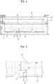
- FIG. 1 is a cross-sectional view illustrating a backlight unit in accordance with one present invention.
- the backlight unit includes a light guide plate 20 having first and second grooves 70 and 24, a reflector 30, optical member 40, and light source modules 50.
- the backlight unit may further include a top chassis 60, a bottom chassis 10, and a panel guide module 80.
- the panel guide module 80 may support a display panel 90, and the top chassis 60 may be connected to the panel guide module 80 and the bottom chassis 10.
- At least one first groove 70 may be disposed on the upper surface of the light guide plate 20, and at least one second groove 24 may be disposed on the lower surface of the light guide plate 20.
- the first groove 70 of the light guide plate 20 may have a hemispheric, triangular, or trapezoidal cross-section.
- the cross-section of the first groove 70 may include a first inclined surface and a second inclined surface meeting at one point.
- the first inclined surface may be a concave surface having a first curvature
- the second inclined surface may be a concave surface having a second curvature
- the first curvature and the second curvature may be different.
- the first inclined surface may be a flat surface inclined at a first angle with respect to the upper surface of the light guide plate 20
- the second inclined surface may be a flat surface inclined at a second angle with respect to the upper surface of the light guide plate 20 and the first angle and the second angle may be different.
- one of the first and second inclined surfaces may be a concave surface having a designated curvature, and the other of the first and second inclined surfaces may be a flat surface inclined at a designated angle with respect to the upper surface of the light guide plate 20.
- the cross-section of the first groove 70 may include a first inclined surface and a second inclined surface, and a flat surface parallel with the upper surface of the light guide plate 20 may be disposed between the first and second inclined surfaces.
- the first groove 70 having the above shape may be disposed at one side of the second groove 24, and may be disposed between light sources 52 of the light source module 50.
- the first groove 70 may have a depth of about 0.1 ⁇ 0.5 mm, and the maximum depth value of the first groove 70 may be smaller than a distance value between the upper surface of the light guide plate 20 and the second groove 24.
- the length of the first groove 70 means a distance between both ends of the first groove 70 disposed in a first direction
- the width of the first groove 70 means a distance between both ends of the first groove 70 in a second direction perpendicular to the first direction
- the length and width of the first groove 70 may be smaller than the distance between the light sources 52 of the light source module 50.
- the length of the first groove 70 may be about 3 ⁇ 7 mm, and the width of the first groove 70 may be about 1 ⁇ 4 mm.
- the second groove 24 disposed on the lower surface of the light guide plate 20 has a trapezoidal cross-section.
- the first side surface of the second groove 24 may be perpendicular to the bottom surface of the second groove 24, and the second side surface of the second groove 24 may be inclined at a first angle with respect to the bottom surface of the second groove 24.
- the first and second side surfaces of the second groove 24 opposite each other may be inclined with respect to the bottom surface of the second groove 24, and an angle between the first side surface and the bottom surface of the second groove 24 may be smaller than an angle between the second side surface and the bottom surface of the second groove 24.
- an angle between first and second side surfaces opposite each other of the second groove 24 may be about 30° to 120°.
- a ratio of the height of the second groove 24 of the light guide plate 20 to the overall thickness of the light guide plate 20 may be about 0.3 ⁇ 0.7:1.
- the light guide plate 20 may be formed of at least one selected from among the group consisting of acrylic resins, such as polymethylmethacrylate (PMMA), polyethylene terephthalate (PET), cyclic olefin copolymers (COCs), polyethylene naphthalate (PEN), polycarbonate (PC), polystyrene (PS) and methacrylate styrene (MS) resins.
- acrylic resins such as polymethylmethacrylate (PMMA), polyethylene terephthalate (PET), cyclic olefin copolymers (COCs), polyethylene naphthalate (PEN), polycarbonate (PC), polystyrene (PS) and methacrylate styrene (MS) resins.
- the light source modules 50 may be disposed within the second grooves 24 of the light guide plate 20.
- each light source module 50 may include a substrate 54 and at least one light source 52 disposed on the substrate 54. Both the substrate 54 and the at least one light source 52 may be disposed within the second groove 24 of the light guide plate 20.
- the substrate 54 may be disposed at the outside of the second groove 24 of the light guide plate 20, and the at least one light source 52 may be disposed within the second groove 24 of the light guide plate 20.
- the substrate 54 may include an electrode pattern to be electrically connected to the light source 52, and may be a printed circuit board (PCB) formed of at least one selected from the group consisting of polyethylene terephthalate (PET), glass, polycarbonate (PC) and silicon (Si), or be formed as a film.
- PCB printed circuit board
- the substrate 54 may selectively employ a single layer PCB, a multilayer PCB, a ceramic substrate, a metal core PCB, etc.
- the at least one light source 52 may be disposed on the substrate 54, and the light source 52 may be a side view type LED.
- the light source 52 may be a top view type LED.
- the light source 52 may be an LED chip, and the LED chip may be a blue LED chip or an ultraviolet LED chip, or a package in which at least one of a red LED chip, a green LED chip, a blue LED chip, a yellow green LED chip and a white LED chip are combined.
- the white LED may be produced by combining a yellow phosphor with a blue LED, by using both a red phosphor and a green phosphor on a blue LED, or by using a yellow phosphor, a red phosphor and a green phosphor on a blue LED.
- the reflector 30 is disposed on the lower surface of the light guide plate 20.
- the reflector 30 may be disposed between the light guide plate 20 and the bottom chassis 10, and may extend from the lower surface to the side surface of the light guide plate 20.
- the reflector 30 is not disposed on the lower surface of the substrate 54 of the light source module 50. However, according to circumstance, the reflector 30 may be disposed on the lower surface of the substrate 54.
- the reflector 30 is disposed on at least one of the side surfaces of the second grooves 24 of the light guide plate 20 and the bottom surfaces of the second grooves 24.
- the reflector 30 may be formed of at least one of a metal and a metal oxide, and for example, may be formed of a metal or a metal oxide exhibiting high reflectivity, such as aluminum (Al), silver (Ag), gold (Au) or titanium oxide (Ti02).
- the optical members 40 may be disposed on the upper surface of the light guide plate 20.
- the optical members 40 serve to diffuse light emitted through the light guide plate 20, and may have an uneven pattern disposed on the upper surface thereof to increase diffusion effects.
- optical members 40 may include several layers, and the uneven pattern may be disposed on the surface of the uppermost layer or one layer.
- the uneven pattern may have a stripe shape disposed along the light source modules 50.
- the uneven pattern includes protrusions protruding from the surface of the optical member 40, and the protrusions include first planes and second planes opposite each other.
- An angle between the first plane and the second plane may be obtuse or acute.
- the optical members 40 may include at least one sheet, i.e., may selectively include a diffusion sheet, a prism sheet, a brightness enhancement sheet, etc.
- the diffusion sheet serves to diffuse light emitted by the light sources
- the prism sheet serves to guide diffused light to a light emission area
- the brightness enhancement sheet serves to enhance brightness of light.
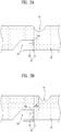
- FIG. 2 is a cross-sectional view illustrating a position at which the first groove of the light guide plate is disposed.
- the first groove 70 may be disposed on the upper surface of the light guide plate 20, and the second groove 24 may be disposed on the lower surface of the light guide plate 20.
- the light source module 50 is disposed within the second groove 24, and the light sources 52 of the light source module 50 may face the side surface of the second groove 24.
- the first groove 70 may be disposed on the upper surface of the light guide plate 20 at one side of the second groove 24 and may be disposed between the light sources 52 of the light source module 50, simultaneously.
- the maximum depth of the first groove 70 means a distance d1 from the upper surface of the light guide plate 20 to the lowermost surface of the first groove 70.
- the maximum depth of the first groove 70 may be smaller than a distance d2 from the upper surface of the light guide plate 20 to the second groove 24.
- the maximum depth of the first groove 70 is greater than the distance d2 from the upper surface of the light guide plate 20 to the second groove 24, light is blocked by the first groove 70 and thus is not diffused to the light guide plate 20, thereby lowering brightness.
- first groove 70 if the depth of the first groove 70 is properly adjusted, light may be refracted by the first groove 70 and be diffused to the inside and outside of the light guide plate 20, and thus dark regions generated at areas between adjacent light sources 52 may be reduced.
- the depth of the first groove 70 may be about 0.1 ⁇ 0.5 mm.
- FIG. 3A to 3C are cross-sectional views illustrating position relations between first grooves and second grooves of the light guide plate.
- one side end of the first groove 70 disposed on the upper surface of the light guide plate 20 may be disposed on an extension line extending from the side surface 24a of the second groove 24.
- dark regions generated between the light sources 52 of the light source module 50 may be generated at the area of the side surface 24a of the second groove 24.
- one side end of the first groove 70 disposed on the upper surface of the light guide plate 20 may be separated from an extension line extending from the side surface 24a of the second groove 24 by a designated interval d3.
- dark regions generated between the light sources 52 of the light source module 50 may be generated at an area separated from the area of the side surface 24a of the second groove 24.
- the first groove 70 disposed on the upper surface of the light guide plate 20 and the second groove 24 disposed on the lower surface of the light guide plate 20 may partially overlap each other by a designated interval d4.
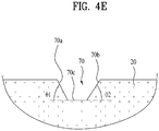
- FIGs. 4A to 4E are cross-sectional views illustrating various shapes of the first grooves of the light guide plate.
- the cross-section of the first groove 70 disposed on the upper surface of the light guide plate 20 may include a first inclined surface 70a and a second inclined surface 70b meeting at one point P1.
- first inclined surface 70a of the first groove 70 may be a concave surface having a first curvature R1
- the second inclined surface 70b of the first groove 70 may be a concave surface having a second curvature R2.
- the first curvature R1 and the second curvature R2 may be different, or be equal.
- the first curvature R1 and the second curvature R2 are different, the first curvature R1 may be greater than the second curvature R2.
- the cross-section of the first groove 70 disposed on the upper surface of the light guide plate 20 may include a first inclined surface 70a and a second inclined surface 70b meeting at one point P1.
- first inclined surface 70a of the first groove 70 may be a concave surface having a first curvature R1
- the second inclined surface 70b of the first groove 70 may be a flat surface inclined at a designated angle ⁇ 2 with respect to the upper surface of the light guide plate 20.
- the cross-section of the first groove 70 disposed on the upper surface of the light guide plate 20 may include a first inclined surface 70a and a second inclined surface 70b meeting at one point P1.
- first inclined surface 70a of the first groove 70 may be a flat surface inclined at a designated angle ⁇ 1 with respect to the upper surface of the light guide plate 20, and the second inclined surface 70b of the first groove 70 may be a flat surface inclined at a designated angle ⁇ 2 with respect to the upper surface of the light guide plate 20.
- the first angle ⁇ 1 and the second angle ⁇ 2 may be different, or be equal.
- the first angle ⁇ 1 and the second angle ⁇ 2 are different, the first angle ⁇ 1 may be greater than the second angle ⁇ 2.
- the cross-section of the first groove 70 disposed on the upper surface of the light guide plate 20 may include a first inclined surface 70a and a second inclined surface 70b meeting at one point P1.
- first inclined surface 70a of the first groove 70 may be a flat surface inclined at a designated angle ⁇ 2 with respect to the upper surface of the light guide plate 20, and the second inclined surface 70b of the first groove 70 may be a concave surface having a second curvature R2.
- the cross-section of the first groove 70 disposed on the upper surface of the light guide plate 20 may include a first inclined surface 70a and a second inclined surface 70b, and a flat surface 70c parallel with the upper surface of the light guide plate 20 may be disposed between the first and second inclined surfaces 70a and 70b.
- first inclined surface 70a of the first groove 70 may be a flat surface inclined at a designated angle ⁇ 1 with respect to the upper surface of the light guide plate 20, and the second inclined surface 70b of the first groove 70 may be a flat surface inclined at a designated angle ⁇ 2 with respect to the upper surface of the light guide plate 20.
- the first angle ⁇ 1 and the second angle ⁇ 2 may be different, or be equal.
- the first angle ⁇ 1 and the second angle ⁇ 2 are different, the first angle ⁇ 1 may be greater than the second angle ⁇ 2.
- first and second angle ⁇ 1 and ⁇ 2 may be about 9 ⁇ 89 degrees.
- FIG. 5 is a plan view illustrating the positions of the first grooves of the light guide plate.
- the first grooves 70 disposed on the upper surface of the light guide plate 20 are separated from each other at a designated interval greater than zero, and be disposed in front of the light source module 50.
- the respective first grooves 70 are disposed between the light sources 52 of the light source module 50.
- the length L1 of the first groove 70 may mean a distance between both ends of the first groove 70 disposed in the first direction (the direction in which the light sources 52 of the light source module 50 are arranged).
- the length L1 of the first groove 70 may be about 3 ⁇ 7 mm.
- the width W1 of the first groove 70 may mean a distance between both ends of the first groove 70 disposed in the second direction perpendicular to the first direction.
- the width W1 of the first groove 70 may be about 1 ⁇ 4 mm.
- the length L1 and the width W1 of the first groove 70 may be smaller than the distance between the light sources 52 of the light source module 50.
- the length L1 and the width W1 of the first groove 70 may be varied according to the distance between the light sources 52 of the light source module 50.
- the first grooves 70 are disposed at dark regions generated between adjacent light sources 52, as described above, light is refracted by the first grooves 70 and thus the dark regions may be reduced, and uniform brightness may be provided.
- FIG. 6 is a plan view illustrating the positions of third grooves of the light guide plate.
- third grooves 72 may be additionally disposed between adjacent first grooves 70 of the light guide plate 20.
- the third grooves 72 may be disposed at positions corresponding to the respective light sources 52 of the light source module 50.
- third grooves 72 may be connected to the adjacent first grooves 70.
- the length L2 of the third groove 72 means a distance between adjacent first grooves 70.
- the length L2 of the third groove 72 may be smaller than the length L1 of the first groove 70 and be greater than the length of the light source 52.
- the width W2 of the third groove 72 means a distance between both ends of the third groove 72 in a direction perpendicular to the lengthwise direction of the third groove 72.
- the width W2 of the third groove 72 may be smaller than the width W1 of the first groove 70.
- the depth of the third groove 72 may be equal to the depth of the first groove 70, or may be different from the depth of the first groove 70 according to circumstance.
- the depth of the third groove 72 may be smaller than the depth of the first groove 70.
- a ratio of the depth of the third groove 72 to the depth of the first groove 70 may be about 1:1.5 ⁇ 3.
- the reason why the third grooves 72 are disposed, as described above, is that, since adjacent first grooves 70 may cause a brightness difference, in order to provide uniform brightness, the brightness difference between the first grooves 70 needs to be reduced.
- the brightness difference may be prevented and dark regions generated in front of the light sources 52 may be reduced.
- the third groove 72 may be separated from an extension line extending from one side of the second groove 24 so as to prevent overlap of the third grooves 72 with the second grooves 24 disposed on the lower surface of the light guide plate 20.
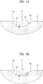
- FIGs. 7A and 7B are views illustrating refraction of light according to presence and absence of the first groove of the light guide plate.
- FIG. 7A illustrates refraction of light if no first groove 70 is disposed on the upper surface of the light guide plate 20
- FIG. 7B illustrates refraction of light if the second groove 24 is disposed on the upper surface of the light guide plate 20.
- the first groove 70 is disposed on the upper surface of the light guide plate 20
- a portion of light diffused to the inside of the light guide plate 20 may be refracted to the outside of the light guide plate 20 by the first groove 70 disposed on the upper surface of the light guide plate 20, and the remaining portion of light may be returned to the inside of the light guide plate 20.
- dark regions generated between the light sources may be reduced by light refracted to the outside of the light guide plate 20 by the first groove 70.
- the present inventions form grooves at dark regions on the upper surface of the light guide plate, and thus reduce dark regions, thereby being capable of providing a backlight unit having uniform brightness.
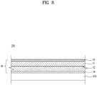
- FIG. 8 is a cross-sectional view illustrating a display module having a backlight unit in accordance with one present invention.
- a display module 200 includes a display panel 90 and a backlight unit 100.
- the display panel 90 includes a color filter substrate 91 and a thin film transistor (TFT) substrate 92 disposed opposite each other and bonded to each other to maintain a uniform cell gap, and a liquid crystal layer (not shown) may be interposed between the two substrates 91 and 92.
- TFT thin film transistor
- the color filter substrate 91 includes a plurality of pixels including red (R), green (G) and blue (B) sub-pixels, and generates an image corresponding to red, green or blue if light is applied to the color filter substrate 91.
- the pixels may include red (R), green (G) and blue (B) sub-pixels
- the present invention is not limited thereto and red (R), green (G), blue (B) and white (W) sub-pixels may form one pixel.
- the TFT substrate 92 includes switching elements, and may switch pixel electrodes (not shown).
- a common electrode (not shown) and the pixel electrodes may change arrangement of molecules of the liquid crystal layer based on a designated voltage applied from the outside.
- the liquid crystal layer may include a plurality of liquid crystal molecules, and arrangement of the liquid crystal molecules is changed due to a voltage difference between the pixel electrodes and the common electrode.
- an upper polarizing plate 93 and a lower polarizing plate 94 may be disposed on the upper surface and the lower surface of the display panel 90, and more particularly, the upper polarizing plate 93 may be disposed on the upper surface of the color filter substrate 91 and the lower polarizing plate 94 may be disposed on the lower surface of the TFT substrate 92.
- gate and data driving units generating driving signals to drive the display panel 90 may be provided on the side surface of the display panel 90.
- the display module 200 may be disposed by disposing the backlight unit 100 close to the display panel 90.
- the backlight unit 100 may be fixed to the lower surface of the display panel 90, more particularly be attached to the lower polarizing plate 94, and for this purpose, an adhesive layer (not shown) may be disposed between the lower polarizing plate 94 and the backlight unit 100.
- the backlight unit 100 By attaching the backlight unit 100 to the display panel 90, as described above, the overall thickness of the display apparatus is reduced, and thus the external appearance of the display apparatus may be improved. Further, additional structures to fix the backlight unit 100 are removed, and thus the structure and manufacturing process of the display apparatus may be simplified.
- FIGs. 9 and 10 are views respectively illustrating display apparatuses in accordance with present inventions.
- a display apparatus 1 includes a display module 200, a front cover 300 and a back cover 350 surrounding the display module 200, a driving unit 550 provided on the back cover 350, and a driving unit cover 400 surrounding the driving unit 550.
- the front cover 300 may include a front panel (not shown) disposed of a transparent material transmitting light.
- the front panel which is separated from the display module 200 at a designated interval protects the display module 200 and transmits light emitted from the display module 200, thereby allowing an image displayed on the display module 200 to be seen from the outside.
- the front cover 300 may be a flat plate without a window 300a.
- the front cover 300 may be disposed of a transparent material transmitting light, for example, of injection molded plastic.
- front cover 300 is a flat plate, a frame may be removed from the front cover 300.
- the back cover 350 may be connected to the front cover 300 to protect the display module 200.
- the driving unit 550 may be disposed on one surface of the back cover 350.
- the driving unit 550 may include a driving control unit 550a, a main board 550b and a power supply unit 550c.
- the driving control unit 550a may be a timing controller, i.e., a driver to control operation timing of respective driver ICs of the display module 200
- the main board 550b may be a driver to transmit a V-sync, an H-sync and R, G and B resolution signals to the timing controller
- the power supply unit 550c may be a driver to apply power to the display module 200.
- the driving unit 550 may be provided on the back cover 350 and be surrounded by the driving unit cover 400.
- the back cover 350 may be provided with a plurality of holes through which the display module 200 and the driving unit 550 are connected to each other, and a stand 600 to support the display apparatus 1 may be provided.
- the driving control unit 550a of the driving unit 550 may be provided on the back cover 350, and the main board 550b and the power supply unit 550c of the driving unit 550 may be provided on the stand 600.
- the driving unit cover 400 may surround only the driving control unit 550a provided on the back cover 350.
- main board 550b and the power supply unit 550c may be integrated into one board.
- Another present invention may implement a display apparatus, an indication apparatus or an illumination system including the light guide plate having the first and second grooves and the light source modules described in accordance with the above-described present inventions, and, for example, the illumination system may include a lamp or a streetlight.
- Such an illumination system may be used as an illumination lamp which concentrates light emitted from plural LEDs, particularly used as a lamp (down light) which is embedded in the ceiling or the wall of a building and is installed to expose an opening of a shade.
- a backlight unit and a display apparatus using the same in accordance with one present invention form grooves at areas where dark regions are generated, thereby reducing the dark regions and thus allowing the backlight unit to have uniform brightness.
Applications Claiming Priority (1)
| Application Number | Priority Date | Filing Date | Title |
|---|---|---|---|
| KR1020110070376A KR101830718B1 (ko) | 2011-07-15 | 2011-07-15 | 디스플레이 장치 |
Publications (2)
| Publication Number | Publication Date |
|---|---|
| EP2546685A1 EP2546685A1 (en) | 2013-01-16 |
| EP2546685B1 true EP2546685B1 (en) | 2018-11-28 |
Family
ID=45656364
Family Applications (1)
| Application Number | Title | Priority Date | Filing Date |
|---|---|---|---|
| EP12156445.4A Not-in-force EP2546685B1 (en) | 2011-07-15 | 2012-02-22 | Backlight unit and display apparatus using the same |
Country Status (6)
| Country | Link |
|---|---|
| US (1) | US20130016521A1 (ja) |
| EP (1) | EP2546685B1 (ja) |
| JP (1) | JP6087508B2 (ja) |
| KR (1) | KR101830718B1 (ja) |
| CN (1) | CN102878477B (ja) |
| TW (1) | TWI570482B (ja) |
Families Citing this family (4)
| Publication number | Priority date | Publication date | Assignee | Title |
|---|---|---|---|---|
| US20150362653A1 (en) * | 2014-06-17 | 2015-12-17 | Shenzhen China Star Optoelectronics Technology Co., Ltd. | Backlight module |
| CN104006337A (zh) * | 2014-06-17 | 2014-08-27 | 深圳市华星光电技术有限公司 | 背光模组 |
| KR101710520B1 (ko) | 2015-10-02 | 2017-02-27 | 한국과학기술원 | 로컬 디밍이 가능한 백라이트 유닛 |
| KR20210015342A (ko) * | 2019-08-01 | 2021-02-10 | 엘지이노텍 주식회사 | 조명 장치 |
Citations (1)
| Publication number | Priority date | Publication date | Assignee | Title |
|---|---|---|---|---|
| US20110050558A1 (en) * | 2009-08-27 | 2011-03-03 | Sangtae Park | Backlight unit and display device |
Family Cites Families (29)
| Publication number | Priority date | Publication date | Assignee | Title |
|---|---|---|---|---|
| US7108414B2 (en) * | 1995-06-27 | 2006-09-19 | Solid State Opto Limited | Light emitting panel assemblies |
| CN1227561C (zh) * | 2002-09-12 | 2005-11-16 | 瀚宇彩晶股份有限公司 | 平面光源装置及液晶显示器 |
| JP2004319340A (ja) * | 2003-04-17 | 2004-11-11 | Kawaguchiko Seimitsu Co Ltd | バックライトユニット |
| TWI257018B (en) * | 2004-07-07 | 2006-06-21 | Epistar Corp | A back light module with independent light source |
| KR20060012959A (ko) * | 2004-08-05 | 2006-02-09 | 삼성전자주식회사 | 표시 장치용 백라이트 |
| WO2006131924A2 (en) * | 2005-06-07 | 2006-12-14 | Oree, Advanced Illumination Solutions Inc. | Illumination apparatus |
| CN101248378B (zh) * | 2005-08-24 | 2011-03-09 | 皇家飞利浦电子股份有限公司 | 照明模块 |
| JP4631628B2 (ja) * | 2005-09-13 | 2011-02-16 | 日本電気株式会社 | 照明装置及び表示装置 |
| JP4600257B2 (ja) * | 2005-11-25 | 2010-12-15 | ソニー株式会社 | 導光板、バックライト装置とその製造方法及び液晶表示装置 |
| KR20070096457A (ko) * | 2006-03-24 | 2007-10-02 | 엘지전자 주식회사 | 광 파이프를 이용한 면 광원 장치, 이를 구비한 백라이트유닛 및 액정 표시 장치 |
| CN101126866B (zh) * | 2006-08-17 | 2010-12-29 | 奇美电子股份有限公司 | 直下式背光模块及包含该背光模块的液晶显示装置 |
| JP4840779B2 (ja) * | 2007-04-19 | 2011-12-21 | スタンレー電気株式会社 | 面光源装置 |
| CN101295038A (zh) * | 2007-04-27 | 2008-10-29 | 鸿富锦精密工业(深圳)有限公司 | 背光模组及其光学板 |
| CN101299113B (zh) * | 2007-04-30 | 2011-06-29 | 鸿富锦精密工业(深圳)有限公司 | 背光模组及其光学板 |
| CN101308225B (zh) * | 2007-05-18 | 2011-07-27 | 鸿富锦精密工业(深圳)有限公司 | 背光模组及其光学板 |
| CN101377589B (zh) * | 2007-08-27 | 2012-03-21 | 奇美电子股份有限公司 | 背光模组及使用此背光模组的液晶显示装置 |
| US7845826B2 (en) * | 2008-01-15 | 2010-12-07 | Skc Haas Display Films Co., Ltd. | Multilayered integrated backlight illumination assembly |
| US8462292B2 (en) * | 2008-07-31 | 2013-06-11 | Rambus Delaware Llc | Optically transmissive substrates and light emitting assemblies and methods of making same, and methods of displaying images using the optically transmissive substrates and light emitting assemblies |
| JP2010073574A (ja) * | 2008-09-19 | 2010-04-02 | Sony Corp | 面光源装置及び表示装置 |
| CN101382254B (zh) * | 2008-10-29 | 2011-11-09 | 友达光电股份有限公司 | 导光板与基于该导光板的背光模块 |
| WO2010058625A1 (ja) * | 2008-11-20 | 2010-05-27 | シャープ株式会社 | 照明装置、表示装置、及びテレビ受信装置 |
| CN102239360A (zh) * | 2008-12-05 | 2011-11-09 | 夏普株式会社 | 照明装置、显示装置和电视接收装置 |
| US8115890B2 (en) * | 2009-01-22 | 2012-02-14 | Hitachi Consumer Electronics Co., Ltd. | Backlight unit and a liquid crystal display apparatus applying the same therein |
| CN101839445B (zh) * | 2009-03-20 | 2013-03-27 | 上海向隆电子科技有限公司 | 背光模块中导光板的区段导光结构 |
| JP4724238B2 (ja) * | 2009-06-18 | 2011-07-13 | 株式会社エス・ケー・ジー | 照明装置 |
| KR20110006773A (ko) * | 2009-07-15 | 2011-01-21 | 삼성전자주식회사 | 디스플레이장치 및 텔레비전 |
| KR101255287B1 (ko) * | 2009-07-16 | 2013-04-15 | 엘지디스플레이 주식회사 | 백라이트 유닛 |
| CN102511012B (zh) * | 2009-09-21 | 2014-10-15 | 皇家飞利浦电子股份有限公司 | 包含具有眩光减弱的反射屏蔽的光导板的发光设备 |
| KR20110068382A (ko) * | 2009-12-16 | 2011-06-22 | 삼성전자주식회사 | 백라이트유닛 및 이를 가지는 디스플레이장치 |
-
2011
- 2011-07-15 KR KR1020110070376A patent/KR101830718B1/ko active IP Right Grant
-
2012
- 2012-02-21 TW TW101105618A patent/TWI570482B/zh not_active IP Right Cessation
- 2012-02-21 US US13/400,943 patent/US20130016521A1/en not_active Abandoned
- 2012-02-22 EP EP12156445.4A patent/EP2546685B1/en not_active Not-in-force
- 2012-02-28 JP JP2012042486A patent/JP6087508B2/ja not_active Expired - Fee Related
- 2012-03-15 CN CN201210068387.5A patent/CN102878477B/zh not_active Expired - Fee Related
Patent Citations (1)
| Publication number | Priority date | Publication date | Assignee | Title |
|---|---|---|---|---|
| US20110050558A1 (en) * | 2009-08-27 | 2011-03-03 | Sangtae Park | Backlight unit and display device |
Also Published As
| Publication number | Publication date |
|---|---|
| JP6087508B2 (ja) | 2017-03-01 |
| EP2546685A1 (en) | 2013-01-16 |
| CN102878477A (zh) | 2013-01-16 |
| KR101830718B1 (ko) | 2018-02-22 |
| US20130016521A1 (en) | 2013-01-17 |
| TW201303449A (zh) | 2013-01-16 |
| CN102878477B (zh) | 2017-05-31 |
| JP2013026213A (ja) | 2013-02-04 |
| KR20130009342A (ko) | 2013-01-23 |
| TWI570482B (zh) | 2017-02-11 |
Similar Documents
| Publication | Publication Date | Title |
|---|---|---|
| US9458992B2 (en) | Backlight unit and display apparatus using the same | |
| US8876315B2 (en) | Lighting apparatus and display apparatus using the same | |
| US9519099B2 (en) | Backlight unit and display apparatus using the same | |
| EP2541136B1 (en) | Backlight unit | |
| EP2546685B1 (en) | Backlight unit and display apparatus using the same | |
| KR20130039406A (ko) | 백라이트 유닛 및 이를 이용한 디스플레이 장치 | |
| KR20130000904A (ko) | 백라이트 유닛 및 그를 이용한 디스플레이 장치 | |
| KR101832308B1 (ko) | 디스플레이 장치 | |
| KR101838020B1 (ko) | 조명 장치 | |
| KR101820692B1 (ko) | 디스플레이 장치 | |
| KR101832307B1 (ko) | 디스플레이 장치 | |
| KR101854852B1 (ko) | 조명 장치 | |
| KR101832309B1 (ko) | 디스플레이 장치 |
Legal Events
| Date | Code | Title | Description |
|---|---|---|---|
| PUAI | Public reference made under article 153(3) epc to a published international application that has entered the european phase |
Free format text: ORIGINAL CODE: 0009012 |
|
| AK | Designated contracting states |
Kind code of ref document: A1 Designated state(s): AL AT BE BG CH CY CZ DE DK EE ES FI FR GB GR HR HU IE IS IT LI LT LU LV MC MK MT NL NO PL PT RO RS SE SI SK SM TR |
|
| AX | Request for extension of the european patent |
Extension state: BA ME |
|
| 17P | Request for examination filed |
Effective date: 20130515 |
|
| 17Q | First examination report despatched |
Effective date: 20160617 |
|
| RAP1 | Party data changed (applicant data changed or rights of an application transferred) |
Owner name: LG INNOTEK CO., LTD. |
|
| STAA | Information on the status of an ep patent application or granted ep patent |
Free format text: STATUS: EXAMINATION IS IN PROGRESS |
|
| GRAP | Despatch of communication of intention to grant a patent |
Free format text: ORIGINAL CODE: EPIDOSNIGR1 |
|
| STAA | Information on the status of an ep patent application or granted ep patent |
Free format text: STATUS: GRANT OF PATENT IS INTENDED |
|
| INTG | Intention to grant announced |
Effective date: 20180703 |
|
| GRAS | Grant fee paid |
Free format text: ORIGINAL CODE: EPIDOSNIGR3 |
|
| GRAA | (expected) grant |
Free format text: ORIGINAL CODE: 0009210 |
|
| STAA | Information on the status of an ep patent application or granted ep patent |
Free format text: STATUS: THE PATENT HAS BEEN GRANTED |
|
| AK | Designated contracting states |
Kind code of ref document: B1 Designated state(s): AL AT BE BG CH CY CZ DE DK EE ES FI FR GB GR HR HU IE IS IT LI LT LU LV MC MK MT NL NO PL PT RO RS SE SI SK SM TR |
|
| REG | Reference to a national code |
Ref country code: GB Ref legal event code: FG4D |
|
| REG | Reference to a national code |
Ref country code: CH Ref legal event code: EP |
|
| REG | Reference to a national code |
Ref country code: AT Ref legal event code: REF Ref document number: 1070893 Country of ref document: AT Kind code of ref document: T Effective date: 20181215 |
|
| REG | Reference to a national code |
Ref country code: DE Ref legal event code: R096 Ref document number: 602012053975 Country of ref document: DE |
|
| REG | Reference to a national code |
Ref country code: IE Ref legal event code: FG4D |
|
| REG | Reference to a national code |
Ref country code: NL Ref legal event code: MP Effective date: 20181128 |
|
| REG | Reference to a national code |
Ref country code: LT Ref legal event code: MG4D |
|
| REG | Reference to a national code |
Ref country code: AT Ref legal event code: MK05 Ref document number: 1070893 Country of ref document: AT Kind code of ref document: T Effective date: 20181128 |
|
| PG25 | Lapsed in a contracting state [announced via postgrant information from national office to epo] |
Ref country code: IS Free format text: LAPSE BECAUSE OF FAILURE TO SUBMIT A TRANSLATION OF THE DESCRIPTION OR TO PAY THE FEE WITHIN THE PRESCRIBED TIME-LIMIT Effective date: 20190328 Ref country code: FI Free format text: LAPSE BECAUSE OF FAILURE TO SUBMIT A TRANSLATION OF THE DESCRIPTION OR TO PAY THE FEE WITHIN THE PRESCRIBED TIME-LIMIT Effective date: 20181128 Ref country code: BG Free format text: LAPSE BECAUSE OF FAILURE TO SUBMIT A TRANSLATION OF THE DESCRIPTION OR TO PAY THE FEE WITHIN THE PRESCRIBED TIME-LIMIT Effective date: 20190228 Ref country code: LT Free format text: LAPSE BECAUSE OF FAILURE TO SUBMIT A TRANSLATION OF THE DESCRIPTION OR TO PAY THE FEE WITHIN THE PRESCRIBED TIME-LIMIT Effective date: 20181128 Ref country code: NO Free format text: LAPSE BECAUSE OF FAILURE TO SUBMIT A TRANSLATION OF THE DESCRIPTION OR TO PAY THE FEE WITHIN THE PRESCRIBED TIME-LIMIT Effective date: 20190228 Ref country code: ES Free format text: LAPSE BECAUSE OF FAILURE TO SUBMIT A TRANSLATION OF THE DESCRIPTION OR TO PAY THE FEE WITHIN THE PRESCRIBED TIME-LIMIT Effective date: 20181128 Ref country code: LV Free format text: LAPSE BECAUSE OF FAILURE TO SUBMIT A TRANSLATION OF THE DESCRIPTION OR TO PAY THE FEE WITHIN THE PRESCRIBED TIME-LIMIT Effective date: 20181128 Ref country code: AT Free format text: LAPSE BECAUSE OF FAILURE TO SUBMIT A TRANSLATION OF THE DESCRIPTION OR TO PAY THE FEE WITHIN THE PRESCRIBED TIME-LIMIT Effective date: 20181128 Ref country code: HR Free format text: LAPSE BECAUSE OF FAILURE TO SUBMIT A TRANSLATION OF THE DESCRIPTION OR TO PAY THE FEE WITHIN THE PRESCRIBED TIME-LIMIT Effective date: 20181128 |
|
| PGFP | Annual fee paid to national office [announced via postgrant information from national office to epo] |
Ref country code: DE Payment date: 20190207 Year of fee payment: 8 |
|
| PG25 | Lapsed in a contracting state [announced via postgrant information from national office to epo] |
Ref country code: GR Free format text: LAPSE BECAUSE OF FAILURE TO SUBMIT A TRANSLATION OF THE DESCRIPTION OR TO PAY THE FEE WITHIN THE PRESCRIBED TIME-LIMIT Effective date: 20190301 Ref country code: SE Free format text: LAPSE BECAUSE OF FAILURE TO SUBMIT A TRANSLATION OF THE DESCRIPTION OR TO PAY THE FEE WITHIN THE PRESCRIBED TIME-LIMIT Effective date: 20181128 Ref country code: AL Free format text: LAPSE BECAUSE OF FAILURE TO SUBMIT A TRANSLATION OF THE DESCRIPTION OR TO PAY THE FEE WITHIN THE PRESCRIBED TIME-LIMIT Effective date: 20181128 Ref country code: RS Free format text: LAPSE BECAUSE OF FAILURE TO SUBMIT A TRANSLATION OF THE DESCRIPTION OR TO PAY THE FEE WITHIN THE PRESCRIBED TIME-LIMIT Effective date: 20181128 Ref country code: PT Free format text: LAPSE BECAUSE OF FAILURE TO SUBMIT A TRANSLATION OF THE DESCRIPTION OR TO PAY THE FEE WITHIN THE PRESCRIBED TIME-LIMIT Effective date: 20190328 |
|
| PG25 | Lapsed in a contracting state [announced via postgrant information from national office to epo] |
Ref country code: NL Free format text: LAPSE BECAUSE OF FAILURE TO SUBMIT A TRANSLATION OF THE DESCRIPTION OR TO PAY THE FEE WITHIN THE PRESCRIBED TIME-LIMIT Effective date: 20181128 |
|
| PG25 | Lapsed in a contracting state [announced via postgrant information from national office to epo] |
Ref country code: IT Free format text: LAPSE BECAUSE OF FAILURE TO SUBMIT A TRANSLATION OF THE DESCRIPTION OR TO PAY THE FEE WITHIN THE PRESCRIBED TIME-LIMIT Effective date: 20181128 Ref country code: DK Free format text: LAPSE BECAUSE OF FAILURE TO SUBMIT A TRANSLATION OF THE DESCRIPTION OR TO PAY THE FEE WITHIN THE PRESCRIBED TIME-LIMIT Effective date: 20181128 Ref country code: PL Free format text: LAPSE BECAUSE OF FAILURE TO SUBMIT A TRANSLATION OF THE DESCRIPTION OR TO PAY THE FEE WITHIN THE PRESCRIBED TIME-LIMIT Effective date: 20181128 Ref country code: CZ Free format text: LAPSE BECAUSE OF FAILURE TO SUBMIT A TRANSLATION OF THE DESCRIPTION OR TO PAY THE FEE WITHIN THE PRESCRIBED TIME-LIMIT Effective date: 20181128 |
|
| REG | Reference to a national code |
Ref country code: DE Ref legal event code: R097 Ref document number: 602012053975 Country of ref document: DE |
|
| PG25 | Lapsed in a contracting state [announced via postgrant information from national office to epo] |
Ref country code: SM Free format text: LAPSE BECAUSE OF FAILURE TO SUBMIT A TRANSLATION OF THE DESCRIPTION OR TO PAY THE FEE WITHIN THE PRESCRIBED TIME-LIMIT Effective date: 20181128 Ref country code: EE Free format text: LAPSE BECAUSE OF FAILURE TO SUBMIT A TRANSLATION OF THE DESCRIPTION OR TO PAY THE FEE WITHIN THE PRESCRIBED TIME-LIMIT Effective date: 20181128 Ref country code: RO Free format text: LAPSE BECAUSE OF FAILURE TO SUBMIT A TRANSLATION OF THE DESCRIPTION OR TO PAY THE FEE WITHIN THE PRESCRIBED TIME-LIMIT Effective date: 20181128 Ref country code: SK Free format text: LAPSE BECAUSE OF FAILURE TO SUBMIT A TRANSLATION OF THE DESCRIPTION OR TO PAY THE FEE WITHIN THE PRESCRIBED TIME-LIMIT Effective date: 20181128 |
|
| REG | Reference to a national code |
Ref country code: CH Ref legal event code: PL |
|
| PLBE | No opposition filed within time limit |
Free format text: ORIGINAL CODE: 0009261 |
|
| STAA | Information on the status of an ep patent application or granted ep patent |
Free format text: STATUS: NO OPPOSITION FILED WITHIN TIME LIMIT |
|
| GBPC | Gb: european patent ceased through non-payment of renewal fee |
Effective date: 20190228 |
|
| PG25 | Lapsed in a contracting state [announced via postgrant information from national office to epo] |
Ref country code: SI Free format text: LAPSE BECAUSE OF FAILURE TO SUBMIT A TRANSLATION OF THE DESCRIPTION OR TO PAY THE FEE WITHIN THE PRESCRIBED TIME-LIMIT Effective date: 20181128 Ref country code: LU Free format text: LAPSE BECAUSE OF NON-PAYMENT OF DUE FEES Effective date: 20190222 Ref country code: MC Free format text: LAPSE BECAUSE OF FAILURE TO SUBMIT A TRANSLATION OF THE DESCRIPTION OR TO PAY THE FEE WITHIN THE PRESCRIBED TIME-LIMIT Effective date: 20181128 |
|
| 26N | No opposition filed |
Effective date: 20190829 |
|
| REG | Reference to a national code |
Ref country code: BE Ref legal event code: MM Effective date: 20190228 |
|
| REG | Reference to a national code |
Ref country code: IE Ref legal event code: MM4A |
|
| PG25 | Lapsed in a contracting state [announced via postgrant information from national office to epo] |
Ref country code: LI Free format text: LAPSE BECAUSE OF NON-PAYMENT OF DUE FEES Effective date: 20190228 Ref country code: CH Free format text: LAPSE BECAUSE OF NON-PAYMENT OF DUE FEES Effective date: 20190228 |
|
| PG25 | Lapsed in a contracting state [announced via postgrant information from national office to epo] |
Ref country code: IE Free format text: LAPSE BECAUSE OF NON-PAYMENT OF DUE FEES Effective date: 20190222 Ref country code: GB Free format text: LAPSE BECAUSE OF NON-PAYMENT OF DUE FEES Effective date: 20190228 |
|
| PG25 | Lapsed in a contracting state [announced via postgrant information from national office to epo] |
Ref country code: FR Free format text: LAPSE BECAUSE OF NON-PAYMENT OF DUE FEES Effective date: 20190228 Ref country code: BE Free format text: LAPSE BECAUSE OF NON-PAYMENT OF DUE FEES Effective date: 20190228 |
|
| PG25 | Lapsed in a contracting state [announced via postgrant information from national office to epo] |
Ref country code: TR Free format text: LAPSE BECAUSE OF FAILURE TO SUBMIT A TRANSLATION OF THE DESCRIPTION OR TO PAY THE FEE WITHIN THE PRESCRIBED TIME-LIMIT Effective date: 20181128 |
|
| PG25 | Lapsed in a contracting state [announced via postgrant information from national office to epo] |
Ref country code: MT Free format text: LAPSE BECAUSE OF NON-PAYMENT OF DUE FEES Effective date: 20190222 |
|
| REG | Reference to a national code |
Ref country code: DE Ref legal event code: R119 Ref document number: 602012053975 Country of ref document: DE |
|
| PG25 | Lapsed in a contracting state [announced via postgrant information from national office to epo] |
Ref country code: DE Free format text: LAPSE BECAUSE OF NON-PAYMENT OF DUE FEES Effective date: 20200901 |
|
| PG25 | Lapsed in a contracting state [announced via postgrant information from national office to epo] |
Ref country code: CY Free format text: LAPSE BECAUSE OF FAILURE TO SUBMIT A TRANSLATION OF THE DESCRIPTION OR TO PAY THE FEE WITHIN THE PRESCRIBED TIME-LIMIT Effective date: 20181128 |
|
| PG25 | Lapsed in a contracting state [announced via postgrant information from national office to epo] |
Ref country code: HU Free format text: LAPSE BECAUSE OF FAILURE TO SUBMIT A TRANSLATION OF THE DESCRIPTION OR TO PAY THE FEE WITHIN THE PRESCRIBED TIME-LIMIT; INVALID AB INITIO Effective date: 20120222 |
|
| PG25 | Lapsed in a contracting state [announced via postgrant information from national office to epo] |
Ref country code: MK Free format text: LAPSE BECAUSE OF FAILURE TO SUBMIT A TRANSLATION OF THE DESCRIPTION OR TO PAY THE FEE WITHIN THE PRESCRIBED TIME-LIMIT Effective date: 20181128 |