EP2535952A2 - Lichtemittierendes Halbleiterbauelemnt - Google Patents
Lichtemittierendes Halbleiterbauelemnt Download PDFInfo
- Publication number
- EP2535952A2 EP2535952A2 EP12156610A EP12156610A EP2535952A2 EP 2535952 A2 EP2535952 A2 EP 2535952A2 EP 12156610 A EP12156610 A EP 12156610A EP 12156610 A EP12156610 A EP 12156610A EP 2535952 A2 EP2535952 A2 EP 2535952A2
- Authority
- EP
- European Patent Office
- Prior art keywords
- layer
- light emitting
- emitting device
- type semiconductor
- layers
- Prior art date
- Legal status (The legal status is an assumption and is not a legal conclusion. Google has not performed a legal analysis and makes no representation as to the accuracy of the status listed.)
- Granted
Links
Images




Classifications
-
- H—ELECTRICITY
- H10—SEMICONDUCTOR DEVICES; ELECTRIC SOLID-STATE DEVICES NOT OTHERWISE PROVIDED FOR
- H10H—INORGANIC LIGHT-EMITTING SEMICONDUCTOR DEVICES HAVING POTENTIAL BARRIERS
- H10H20/00—Individual inorganic light-emitting semiconductor devices having potential barriers, e.g. light-emitting diodes [LED]
- H10H20/80—Constructional details
- H10H20/81—Bodies
- H10H20/811—Bodies having quantum effect structures or superlattices, e.g. tunnel junctions
- H10H20/812—Bodies having quantum effect structures or superlattices, e.g. tunnel junctions within the light-emitting regions, e.g. having quantum confinement structures
-
- H—ELECTRICITY
- H10—SEMICONDUCTOR DEVICES; ELECTRIC SOLID-STATE DEVICES NOT OTHERWISE PROVIDED FOR
- H10H—INORGANIC LIGHT-EMITTING SEMICONDUCTOR DEVICES HAVING POTENTIAL BARRIERS
- H10H20/00—Individual inorganic light-emitting semiconductor devices having potential barriers, e.g. light-emitting diodes [LED]
- H10H20/80—Constructional details
- H10H20/81—Bodies
- H10H20/811—Bodies having quantum effect structures or superlattices, e.g. tunnel junctions
-
- F—MECHANICAL ENGINEERING; LIGHTING; HEATING; WEAPONS; BLASTING
- F21—LIGHTING
- F21K—NON-ELECTRIC LIGHT SOURCES USING LUMINESCENCE; LIGHT SOURCES USING ELECTROCHEMILUMINESCENCE; LIGHT SOURCES USING CHARGES OF COMBUSTIBLE MATERIAL; LIGHT SOURCES USING SEMICONDUCTOR DEVICES AS LIGHT-GENERATING ELEMENTS; LIGHT SOURCES NOT OTHERWISE PROVIDED FOR
- F21K9/00—Light sources using semiconductor devices as light-generating elements, e.g. using light-emitting diodes [LED] or lasers
- F21K9/20—Light sources comprising attachment means
- F21K9/23—Retrofit light sources for lighting devices with a single fitting for each light source, e.g. for substitution of incandescent lamps with bayonet or threaded fittings
-
- F—MECHANICAL ENGINEERING; LIGHTING; HEATING; WEAPONS; BLASTING
- F21—LIGHTING
- F21V—FUNCTIONAL FEATURES OR DETAILS OF LIGHTING DEVICES OR SYSTEMS THEREOF; STRUCTURAL COMBINATIONS OF LIGHTING DEVICES WITH OTHER ARTICLES, NOT OTHERWISE PROVIDED FOR
- F21V29/00—Protecting lighting devices from thermal damage; Cooling or heating arrangements specially adapted for lighting devices or systems
- F21V29/50—Cooling arrangements
- F21V29/502—Cooling arrangements characterised by the adaptation for cooling of specific components
- F21V29/507—Cooling arrangements characterised by the adaptation for cooling of specific components of means for protecting lighting devices from damage, e.g. housings
-
- F—MECHANICAL ENGINEERING; LIGHTING; HEATING; WEAPONS; BLASTING
- F21—LIGHTING
- F21V—FUNCTIONAL FEATURES OR DETAILS OF LIGHTING DEVICES OR SYSTEMS THEREOF; STRUCTURAL COMBINATIONS OF LIGHTING DEVICES WITH OTHER ARTICLES, NOT OTHERWISE PROVIDED FOR
- F21V29/00—Protecting lighting devices from thermal damage; Cooling or heating arrangements specially adapted for lighting devices or systems
- F21V29/50—Cooling arrangements
- F21V29/70—Cooling arrangements characterised by passive heat-dissipating elements, e.g. heat-sinks
- F21V29/83—Cooling arrangements characterised by passive heat-dissipating elements, e.g. heat-sinks the elements having apertures, ducts or channels, e.g. heat radiation holes
-
- F—MECHANICAL ENGINEERING; LIGHTING; HEATING; WEAPONS; BLASTING
- F21—LIGHTING
- F21Y—INDEXING SCHEME ASSOCIATED WITH SUBCLASSES F21K, F21L, F21S and F21V, RELATING TO THE FORM OR THE KIND OF THE LIGHT SOURCES OR OF THE COLOUR OF THE LIGHT EMITTED
- F21Y2115/00—Light-generating elements of semiconductor light sources
- F21Y2115/10—Light-emitting diodes [LED]
-
- H—ELECTRICITY
- H10—SEMICONDUCTOR DEVICES; ELECTRIC SOLID-STATE DEVICES NOT OTHERWISE PROVIDED FOR
- H10H—INORGANIC LIGHT-EMITTING SEMICONDUCTOR DEVICES HAVING POTENTIAL BARRIERS
- H10H20/00—Individual inorganic light-emitting semiconductor devices having potential barriers, e.g. light-emitting diodes [LED]
- H10H20/80—Constructional details
- H10H20/81—Bodies
- H10H20/822—Materials of the light-emitting regions
- H10H20/824—Materials of the light-emitting regions comprising only Group III-V materials, e.g. GaP
- H10H20/825—Materials of the light-emitting regions comprising only Group III-V materials, e.g. GaP containing nitrogen, e.g. GaN
-
- H—ELECTRICITY
- H10—SEMICONDUCTOR DEVICES; ELECTRIC SOLID-STATE DEVICES NOT OTHERWISE PROVIDED FOR
- H10W—GENERIC PACKAGES, INTERCONNECTIONS, CONNECTORS OR OTHER CONSTRUCTIONAL DETAILS OF DEVICES COVERED BY CLASS H10
- H10W74/00—Encapsulations, e.g. protective coatings
Definitions
- a light emitting device includes a first conductive type semiconductor layer; a second conductive type semiconductor layer disposed on the first conductive type semiconductor layer; and an active layer disposed between the first conductive type semiconductor layer and the second conductive type semiconductor layer, the active layer comprising quantum well layers and quantum barrier layers, wherein each of the quantum well barrier layers comprises first barrier layers and a second barrier layer disposed between the first barrier layers, and an energy bandgap of the second barrier layer is larger than energy bandgaps of the quantum well layers and smaller than energy bandgaps of the first barrier layers.
- the first barrier layers may be layers where an electron or a hole is tunneled.
- the thickness of the quantum well protection layer may be 1nm or less.
- the thickness of the principal quantum barrier protection layer may be 5nm or less.
- the principal barrier layer may be a non-luminous layer.
- the light emitting device may further include a substrate disposed under the first conductive type semiconductor layer; a conductive layer disposed on the second conductive type semiconductor layer; a first electrode disposed on the first conductive type semiconductor layer; and a second electrode disposed on the conductive layer.
- the light emitting device may further include an ohmic layer disposed under the second conductive type semiconductor layer; a reflection layer disposed under the ohmic layer; a first electrode disposed on the first conductive type semiconductor layer; and a passivation layer disposed on a lateral surface of the light emitting structure.
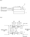
- the quantum well layers QW1 to QWn may be disposed, spaced apart a predetermined distance from the first conductive type semiconductor layer 122 toward the second conductive type semiconductor layer 126.
- the quantum barrier layers QB1 to QBm may be disposed between two neighboring ones of the quantum well layers QW1 to QWn (n ⁇ 2 and 'n' is a natural number), respectively.
- the active layer 124 may include a plurality of quantum well layers QW1 to QWn (n ⁇ 2 and 'n' is a natural number) and quantum barrier layers QBm (m ⁇ 1 and 'm' is a natural number).
- the energy bandgap of the quantum barrier layers QB1 to QBm (m ⁇ 1 and 'm' is a natural number) may be larger than the energy bandgap of the quantum well layers QW1 to QWn (n ⁇ 2 and 'n' is a natural number).
- the first quantum well layer QW1, the second quantum well layer QW2 and the third quantum well layer QW3 may be sequentially disposed adjacent to the electron injecting layer.
- the first quantum barrier layer QB1 may be disposed between the first quantum well layer QW1 and the second quantum well layer QW2 and the second quantum barrier layer QB2 may be disposed between the second quantum well layer QW2 and the third quantum well layer QW3.
- the first quantum well barrier layer QB1 may include a first tunneling barrier layer TB1, a first principal quantum barrier layer mB1 and a second tunneling barrier layer TB2.
- the second quantum barrier layer QB2 may include a third tunneling barrier layer TB3, a second principal quantum barrier layer MB2 and a fourth tunneling barrier layer TB4.
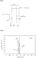
- the first tunneling barrier layer TB1 may be growing until it has a thickness of 1nm or less to have an indium content of less than 5% at the same growth temperature (for example, 700 ⁇ ⁇ 800 ⁇ ) as that of the first quantum well layer QW1.
- the second tunneling barrier layer TB2 may be employed to block the indium included in the first principal quantum barrier layer MB1 from flowing toward the second quantum well layer QW2, only to maintain the indium content of the first principal quantum barrier layer MB1 and to maintain the crystallinity quality of the first principal quantum barrier layer MB1.
- the second tunneling barrier layer TB2 may be referenced to as 'principal quantum barrier protection layer'.
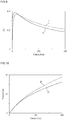
- the output power and the internal quantum efficiency of the embodiment may be improved when the current is injected.
- the ohmic layer 225 may be disposed on the reflective layer 220 and the ohmic layer 225 may in ohmic-contact with a second conductive type semiconductor layer 242 of the light emitting structure 240, to enable the electric power supplied to the light emitting structure 240 smoothly.
- the protection layer 230 may be disposed on the second electrode layer 205 and the protection layer 230 may reduce a surface between the light emitting structure 240 and the adhesive layer 215 from being separated, which might result in deterioration of reliability of the light emitting device 200.
- radiation may be generated in each of the quantum well layers (QW1 to QW3, for example) in the light emitting device 200 according to this embodiment, when the current is injected. Because of that, internal quantum efficiency may be enhanced and an output power may be enhanced.
- the first metal layer 512 and the second metal layer 514 may be disposed on a surface of the package body 510, electrically separable from each other.
- the light emitting device 520 may be electrically connected with the first metal layer 512 and the second metal layer 514. At this time, the light emitting device 520 may be the light emitting device 100 or 200 shown in FIG. 1 or 11 .
- the optical member 840 may be provided on the light guide plate 830 to diffuse the light emitted from the light guide plate 830 at a preset angle.
- the optical member 840 may enable the light guided by the light guide plate 830 to be radiated toward the liquid crystal display panel 860 uniformly.
- an optical sheet such as a diffusion sheet, a prism sheet or a protection sheet may be selectively multilayered or a micro lens array may be used.
- a plurality of optical sheets may be used and the optical sheets may be formed of transparent resin such as acryl resin, polyurethane resin or silicon resin.
- a phosphor sheet may be provided in the prism sheet mentioned above, as mentioned above.
Landscapes
- Led Devices (AREA)
Applications Claiming Priority (1)
| Application Number | Priority Date | Filing Date | Title |
|---|---|---|---|
| KR1020110057373A KR20120138080A (ko) | 2011-06-14 | 2011-06-14 | 발광 소자 |
Publications (3)
| Publication Number | Publication Date |
|---|---|
| EP2535952A2 true EP2535952A2 (de) | 2012-12-19 |
| EP2535952A3 EP2535952A3 (de) | 2016-12-21 |
| EP2535952B1 EP2535952B1 (de) | 2019-11-06 |
Family
ID=45656479
Family Applications (1)
| Application Number | Title | Priority Date | Filing Date |
|---|---|---|---|
| EP12156610.3A Active EP2535952B1 (de) | 2011-06-14 | 2012-02-22 | Lichtemittierendes Halbleiterbauelemnt |
Country Status (4)
| Country | Link |
|---|---|
| US (1) | US9337383B2 (de) |
| EP (1) | EP2535952B1 (de) |
| KR (1) | KR20120138080A (de) |
| CN (1) | CN102832305B (de) |
Families Citing this family (10)
| Publication number | Priority date | Publication date | Assignee | Title |
|---|---|---|---|---|
| KR101865405B1 (ko) * | 2011-10-13 | 2018-06-07 | 엘지이노텍 주식회사 | 발광소자 |
| CN103594573B (zh) * | 2013-11-12 | 2016-05-04 | 西安神光皓瑞光电科技有限公司 | 一种高亮度发光二极管的多量子阱结构 |
| CN104617487A (zh) * | 2015-01-12 | 2015-05-13 | 中国科学院半导体研究所 | 氮化镓同质衬底上激光器量子阱有源区的同温生长方法 |
| KR102303459B1 (ko) * | 2015-03-11 | 2021-09-17 | 쑤저우 레킨 세미컨덕터 컴퍼니 리미티드 | 발광소자, 발광소자 패키지, 및 이를 포함하는 조명시스템 |
| CN105429002B (zh) * | 2015-11-23 | 2018-10-19 | 深圳瑞波光电子有限公司 | 一种量子阱半导体激光外延结构及量子阱激光器 |
| CN105405947B (zh) * | 2015-12-14 | 2017-12-15 | 华灿光电股份有限公司 | 新型发光二极管外延片及其制备方法 |
| KR102486331B1 (ko) * | 2016-01-07 | 2023-01-10 | 쑤저우 레킨 세미컨덕터 컴퍼니 리미티드 | 발광소자 |
| CN108303819B (zh) * | 2017-01-12 | 2020-11-24 | 京东方科技集团股份有限公司 | 背光源及其制造方法、导光板及其制造方法及显示装置 |
| CN110518100A (zh) * | 2019-08-28 | 2019-11-29 | 映瑞光电科技(上海)有限公司 | GaN基发光二极管外延结构及其制备方法 |
| JP2023184145A (ja) * | 2022-06-17 | 2023-12-28 | 日亜化学工業株式会社 | 窒化物半導体発光素子 |
Family Cites Families (21)
| Publication number | Priority date | Publication date | Assignee | Title |
|---|---|---|---|---|
| US5583878A (en) * | 1993-06-23 | 1996-12-10 | The Furukawa Electric Co., Ltd. | Semiconductor optical device |
| JPH0888434A (ja) * | 1994-09-19 | 1996-04-02 | Mitsubishi Electric Corp | 半導体レーザ,及びその製造方法 |
| JP3014339B2 (ja) * | 1997-04-25 | 2000-02-28 | カナレ電気株式会社 | 量子波干渉層を有した半導体素子 |
| JP2000174328A (ja) | 1998-12-03 | 2000-06-23 | Oki Electric Ind Co Ltd | 垂直微小共振器型発光ダイオード |
| JP4285949B2 (ja) * | 2002-06-27 | 2009-06-24 | シャープ株式会社 | 窒化物半導体発光素子 |
| JP4284946B2 (ja) * | 2002-08-27 | 2009-06-24 | ソニー株式会社 | 窒化物系半導体発光素子 |
| US6995389B2 (en) * | 2003-06-18 | 2006-02-07 | Lumileds Lighting, U.S., Llc | Heterostructures for III-nitride light emitting devices |
| WO2005020396A1 (ja) * | 2003-08-26 | 2005-03-03 | Sony Corporation | GaN系III−V族化合物半導体発光素子及びその製造方法 |
| KR100703096B1 (ko) * | 2005-10-17 | 2007-04-06 | 삼성전기주식회사 | 질화물 반도체 발광 소자 |
| KR100649749B1 (ko) * | 2005-10-25 | 2006-11-27 | 삼성전기주식회사 | 질화물 반도체 발광 소자 |
| JP2007214221A (ja) * | 2006-02-08 | 2007-08-23 | Sharp Corp | 窒化物半導体レーザ素子 |
| US7977665B2 (en) * | 2006-07-26 | 2011-07-12 | Lg Electronics Inc. & Lg Innotek Co., Ltd. | Nitride-based light emitting device |
| CN100485988C (zh) * | 2006-10-18 | 2009-05-06 | 武汉华灿光电有限公司 | 增加内量子效率的半导体发光二极管的量子阱结构 |
| US7649195B2 (en) * | 2007-06-12 | 2010-01-19 | Seoul Opto Device Co., Ltd. | Light emitting diode having active region of multi quantum well structure |
| KR101393897B1 (ko) * | 2007-08-29 | 2014-05-13 | 엘지이노텍 주식회사 | 반도체 발광소자 및 그 제조방법 |
| JP2011517099A (ja) * | 2008-04-04 | 2011-05-26 | ザ リージェンツ オブ ザ ユニバーシティ オブ カリフォルニア | プレーナー半極性(Al,In,Ga,B)Nベースの発光ダイオード向けMOCVD成長技術 |
| KR20090117538A (ko) * | 2008-05-09 | 2009-11-12 | 삼성전기주식회사 | 질화물 반도체 발광소자 |
| JP5044692B2 (ja) * | 2009-08-17 | 2012-10-10 | 株式会社東芝 | 窒化物半導体発光素子 |
| KR101007087B1 (ko) * | 2009-10-26 | 2011-01-10 | 엘지이노텍 주식회사 | 발광소자 및 그 제조방법 |
| KR100969127B1 (ko) * | 2010-02-18 | 2010-07-09 | 엘지이노텍 주식회사 | 발광 소자, 발광 소자 제조방법 및 발광 소자 패키지 |
| US8837547B2 (en) * | 2011-03-17 | 2014-09-16 | Finisar Corporation | Lasers with InGaAs quantum wells with InGaP barrier layers with reduced decomposition |
-
2011
- 2011-06-14 KR KR1020110057373A patent/KR20120138080A/ko not_active Ceased
-
2012
- 2012-02-22 EP EP12156610.3A patent/EP2535952B1/de active Active
- 2012-02-24 US US13/404,615 patent/US9337383B2/en active Active
- 2012-03-08 CN CN201210060331.5A patent/CN102832305B/zh active Active
Non-Patent Citations (1)
| Title |
|---|
| None |
Also Published As
| Publication number | Publication date |
|---|---|
| EP2535952A3 (de) | 2016-12-21 |
| US9337383B2 (en) | 2016-05-10 |
| CN102832305B (zh) | 2017-12-12 |
| EP2535952B1 (de) | 2019-11-06 |
| US20120319079A1 (en) | 2012-12-20 |
| CN102832305A (zh) | 2012-12-19 |
| KR20120138080A (ko) | 2012-12-24 |
Similar Documents
| Publication | Publication Date | Title |
|---|---|---|
| EP2535952B1 (de) | Lichtemittierendes Halbleiterbauelemnt | |
| EP2455987B1 (de) | Lichtemittierende Vorrichtung und Beleuchtungssystem damit | |
| US8723158B2 (en) | Light emitting diode, light emitting device package including the same and lighting system | |
| US20140054542A1 (en) | Light emitting device, light emitting device package and lighting system | |
| US20130105827A1 (en) | Light emitting device | |
| EP2830094B1 (de) | Lichtemittierende Vorrichtung | |
| US8536606B2 (en) | Light emitting device, light emitting device package including the same and lighting system | |
| US8431944B2 (en) | Light emitting device, light emitting device package, and lighting system | |
| EP2858127B1 (de) | Leuchtdiode | |
| CN102881787B (zh) | 发光器件及其制造方法和发光器件封装 | |
| KR101850433B1 (ko) | 발광 소자 | |
| KR20130065096A (ko) | 발광 소자 | |
| KR101861636B1 (ko) | 발광 소자 | |
| KR20130070857A (ko) | 발광 소자 및 그를 이용한 조명 시스템 | |
| KR101838022B1 (ko) | 발광 소자 | |
| KR101888605B1 (ko) | 발광 소자 | |
| KR102239624B1 (ko) | 발광 소자 | |
| KR20130019956A (ko) | 발광소자 패키지 및 이를 포함하는 조명시스템 | |
| KR20130011168A (ko) | 발광소자, 발광 소자 제조방법 및 발광 소자 패키지 | |
| KR20120068295A (ko) | 발광 소자 | |
| KR20130064251A (ko) | 발광 소자 | |
| KR20130061343A (ko) | 발광소자 |
Legal Events
| Date | Code | Title | Description |
|---|---|---|---|
| PUAI | Public reference made under article 153(3) epc to a published international application that has entered the european phase |
Free format text: ORIGINAL CODE: 0009012 |
|
| AK | Designated contracting states |
Kind code of ref document: A2 Designated state(s): AL AT BE BG CH CY CZ DE DK EE ES FI FR GB GR HR HU IE IS IT LI LT LU LV MC MK MT NL NO PL PT RO RS SE SI SK SM TR |
|
| AX | Request for extension of the european patent |
Extension state: BA ME |
|
| 17P | Request for examination filed |
Effective date: 20140328 |
|
| RBV | Designated contracting states (corrected) |
Designated state(s): AL AT BE BG CH CY CZ DE DK EE ES FI FR GB GR HR HU IE IS IT LI LT LU LV MC MK MT NL NO PL PT RO RS SE SI SK SM TR |
|
| RAP1 | Party data changed (applicant data changed or rights of an application transferred) |
Owner name: LG INNOTEK CO., LTD. |
|
| REG | Reference to a national code |
Ref country code: DE Ref legal event code: R079 Ref document number: 602012065377 Country of ref document: DE Free format text: PREVIOUS MAIN CLASS: H01L0033060000 Ipc: H01L0033000000 |
|
| PUAL | Search report despatched |
Free format text: ORIGINAL CODE: 0009013 |
|
| AK | Designated contracting states |
Kind code of ref document: A3 Designated state(s): AL AT BE BG CH CY CZ DE DK EE ES FI FR GB GR HR HU IE IS IT LI LT LU LV MC MK MT NL NO PL PT RO RS SE SI SK SM TR |
|
| AX | Request for extension of the european patent |
Extension state: BA ME |
|
| RIC1 | Information provided on ipc code assigned before grant |
Ipc: H01L 33/06 20100101ALI20161117BHEP Ipc: H01S 5/343 20060101ALI20161117BHEP Ipc: H01L 33/32 20100101ALN20161117BHEP Ipc: G02F 1/13357 20060101ALN20161117BHEP Ipc: F21S 13/00 20060101ALN20161117BHEP Ipc: H01L 33/00 20100101AFI20161117BHEP Ipc: H01L 33/48 20100101ALN20161117BHEP |
|
| RAP1 | Party data changed (applicant data changed or rights of an application transferred) |
Owner name: LG INNOTEK CO., LTD. |
|
| GRAP | Despatch of communication of intention to grant a patent |
Free format text: ORIGINAL CODE: EPIDOSNIGR1 |
|
| STAA | Information on the status of an ep patent application or granted ep patent |
Free format text: STATUS: GRANT OF PATENT IS INTENDED |
|
| INTG | Intention to grant announced |
Effective date: 20190417 |
|
| RAP1 | Party data changed (applicant data changed or rights of an application transferred) |
Owner name: LG INNOTEK CO., LTD. Owner name: INDUSTRY-UNIVERSITY COOPERATION FOUNDATION HANYANG |
|
| GRAJ | Information related to disapproval of communication of intention to grant by the applicant or resumption of examination proceedings by the epo deleted |
Free format text: ORIGINAL CODE: EPIDOSDIGR1 |
|
| GRAP | Despatch of communication of intention to grant a patent |
Free format text: ORIGINAL CODE: EPIDOSNIGR1 |
|
| INTG | Intention to grant announced |
Effective date: 20190612 |
|
| GRAS | Grant fee paid |
Free format text: ORIGINAL CODE: EPIDOSNIGR3 |
|
| GRAA | (expected) grant |
Free format text: ORIGINAL CODE: 0009210 |
|
| STAA | Information on the status of an ep patent application or granted ep patent |
Free format text: STATUS: THE PATENT HAS BEEN GRANTED |
|
| AK | Designated contracting states |
Kind code of ref document: B1 Designated state(s): AL AT BE BG CH CY CZ DE DK EE ES FI FR GB GR HR HU IE IS IT LI LT LU LV MC MK MT NL NO PL PT RO RS SE SI SK SM TR |
|
| REG | Reference to a national code |
Ref country code: GB Ref legal event code: FG4D |
|
| REG | Reference to a national code |
Ref country code: CH Ref legal event code: EP Ref country code: AT Ref legal event code: REF Ref document number: 1199993 Country of ref document: AT Kind code of ref document: T Effective date: 20191115 |
|
| REG | Reference to a national code |
Ref country code: IE Ref legal event code: FG4D |
|
| REG | Reference to a national code |
Ref country code: DE Ref legal event code: R096 Ref document number: 602012065377 Country of ref document: DE |
|
| REG | Reference to a national code |
Ref country code: NL Ref legal event code: MP Effective date: 20191106 |
|
| REG | Reference to a national code |
Ref country code: LT Ref legal event code: MG4D |
|
| PG25 | Lapsed in a contracting state [announced via postgrant information from national office to epo] |
Ref country code: FI Free format text: LAPSE BECAUSE OF FAILURE TO SUBMIT A TRANSLATION OF THE DESCRIPTION OR TO PAY THE FEE WITHIN THE PRESCRIBED TIME-LIMIT Effective date: 20191106 Ref country code: BG Free format text: LAPSE BECAUSE OF FAILURE TO SUBMIT A TRANSLATION OF THE DESCRIPTION OR TO PAY THE FEE WITHIN THE PRESCRIBED TIME-LIMIT Effective date: 20200206 Ref country code: NL Free format text: LAPSE BECAUSE OF FAILURE TO SUBMIT A TRANSLATION OF THE DESCRIPTION OR TO PAY THE FEE WITHIN THE PRESCRIBED TIME-LIMIT Effective date: 20191106 Ref country code: LV Free format text: LAPSE BECAUSE OF FAILURE TO SUBMIT A TRANSLATION OF THE DESCRIPTION OR TO PAY THE FEE WITHIN THE PRESCRIBED TIME-LIMIT Effective date: 20191106 Ref country code: SE Free format text: LAPSE BECAUSE OF FAILURE TO SUBMIT A TRANSLATION OF THE DESCRIPTION OR TO PAY THE FEE WITHIN THE PRESCRIBED TIME-LIMIT Effective date: 20191106 Ref country code: PT Free format text: LAPSE BECAUSE OF FAILURE TO SUBMIT A TRANSLATION OF THE DESCRIPTION OR TO PAY THE FEE WITHIN THE PRESCRIBED TIME-LIMIT Effective date: 20200306 Ref country code: GR Free format text: LAPSE BECAUSE OF FAILURE TO SUBMIT A TRANSLATION OF THE DESCRIPTION OR TO PAY THE FEE WITHIN THE PRESCRIBED TIME-LIMIT Effective date: 20200207 Ref country code: NO Free format text: LAPSE BECAUSE OF FAILURE TO SUBMIT A TRANSLATION OF THE DESCRIPTION OR TO PAY THE FEE WITHIN THE PRESCRIBED TIME-LIMIT Effective date: 20200206 Ref country code: LT Free format text: LAPSE BECAUSE OF FAILURE TO SUBMIT A TRANSLATION OF THE DESCRIPTION OR TO PAY THE FEE WITHIN THE PRESCRIBED TIME-LIMIT Effective date: 20191106 Ref country code: PL Free format text: LAPSE BECAUSE OF FAILURE TO SUBMIT A TRANSLATION OF THE DESCRIPTION OR TO PAY THE FEE WITHIN THE PRESCRIBED TIME-LIMIT Effective date: 20191106 Ref country code: ES Free format text: LAPSE BECAUSE OF FAILURE TO SUBMIT A TRANSLATION OF THE DESCRIPTION OR TO PAY THE FEE WITHIN THE PRESCRIBED TIME-LIMIT Effective date: 20191106 |
|
| PG25 | Lapsed in a contracting state [announced via postgrant information from national office to epo] |
Ref country code: IS Free format text: LAPSE BECAUSE OF FAILURE TO SUBMIT A TRANSLATION OF THE DESCRIPTION OR TO PAY THE FEE WITHIN THE PRESCRIBED TIME-LIMIT Effective date: 20200306 Ref country code: HR Free format text: LAPSE BECAUSE OF FAILURE TO SUBMIT A TRANSLATION OF THE DESCRIPTION OR TO PAY THE FEE WITHIN THE PRESCRIBED TIME-LIMIT Effective date: 20191106 Ref country code: RS Free format text: LAPSE BECAUSE OF FAILURE TO SUBMIT A TRANSLATION OF THE DESCRIPTION OR TO PAY THE FEE WITHIN THE PRESCRIBED TIME-LIMIT Effective date: 20191106 |
|
| PG25 | Lapsed in a contracting state [announced via postgrant information from national office to epo] |
Ref country code: AL Free format text: LAPSE BECAUSE OF FAILURE TO SUBMIT A TRANSLATION OF THE DESCRIPTION OR TO PAY THE FEE WITHIN THE PRESCRIBED TIME-LIMIT Effective date: 20191106 |
|
| PG25 | Lapsed in a contracting state [announced via postgrant information from national office to epo] |
Ref country code: DK Free format text: LAPSE BECAUSE OF FAILURE TO SUBMIT A TRANSLATION OF THE DESCRIPTION OR TO PAY THE FEE WITHIN THE PRESCRIBED TIME-LIMIT Effective date: 20191106 Ref country code: EE Free format text: LAPSE BECAUSE OF FAILURE TO SUBMIT A TRANSLATION OF THE DESCRIPTION OR TO PAY THE FEE WITHIN THE PRESCRIBED TIME-LIMIT Effective date: 20191106 Ref country code: RO Free format text: LAPSE BECAUSE OF FAILURE TO SUBMIT A TRANSLATION OF THE DESCRIPTION OR TO PAY THE FEE WITHIN THE PRESCRIBED TIME-LIMIT Effective date: 20191106 Ref country code: CZ Free format text: LAPSE BECAUSE OF FAILURE TO SUBMIT A TRANSLATION OF THE DESCRIPTION OR TO PAY THE FEE WITHIN THE PRESCRIBED TIME-LIMIT Effective date: 20191106 |
|
| REG | Reference to a national code |
Ref country code: DE Ref legal event code: R097 Ref document number: 602012065377 Country of ref document: DE |
|
| REG | Reference to a national code |
Ref country code: AT Ref legal event code: MK05 Ref document number: 1199993 Country of ref document: AT Kind code of ref document: T Effective date: 20191106 |
|
| PG25 | Lapsed in a contracting state [announced via postgrant information from national office to epo] |
Ref country code: SK Free format text: LAPSE BECAUSE OF FAILURE TO SUBMIT A TRANSLATION OF THE DESCRIPTION OR TO PAY THE FEE WITHIN THE PRESCRIBED TIME-LIMIT Effective date: 20191106 Ref country code: SM Free format text: LAPSE BECAUSE OF FAILURE TO SUBMIT A TRANSLATION OF THE DESCRIPTION OR TO PAY THE FEE WITHIN THE PRESCRIBED TIME-LIMIT Effective date: 20191106 |
|
| PLBE | No opposition filed within time limit |
Free format text: ORIGINAL CODE: 0009261 |
|
| STAA | Information on the status of an ep patent application or granted ep patent |
Free format text: STATUS: NO OPPOSITION FILED WITHIN TIME LIMIT |
|
| REG | Reference to a national code |
Ref country code: CH Ref legal event code: PL |
|
| 26N | No opposition filed |
Effective date: 20200807 |
|
| GBPC | Gb: european patent ceased through non-payment of renewal fee |
Effective date: 20200222 |
|
| REG | Reference to a national code |
Ref country code: BE Ref legal event code: MM Effective date: 20200229 |
|
| PG25 | Lapsed in a contracting state [announced via postgrant information from national office to epo] |
Ref country code: MC Free format text: LAPSE BECAUSE OF FAILURE TO SUBMIT A TRANSLATION OF THE DESCRIPTION OR TO PAY THE FEE WITHIN THE PRESCRIBED TIME-LIMIT Effective date: 20191106 Ref country code: LU Free format text: LAPSE BECAUSE OF NON-PAYMENT OF DUE FEES Effective date: 20200222 |
|
| PG25 | Lapsed in a contracting state [announced via postgrant information from national office to epo] |
Ref country code: LI Free format text: LAPSE BECAUSE OF NON-PAYMENT OF DUE FEES Effective date: 20200229 Ref country code: AT Free format text: LAPSE BECAUSE OF FAILURE TO SUBMIT A TRANSLATION OF THE DESCRIPTION OR TO PAY THE FEE WITHIN THE PRESCRIBED TIME-LIMIT Effective date: 20191106 Ref country code: SI Free format text: LAPSE BECAUSE OF FAILURE TO SUBMIT A TRANSLATION OF THE DESCRIPTION OR TO PAY THE FEE WITHIN THE PRESCRIBED TIME-LIMIT Effective date: 20191106 Ref country code: CH Free format text: LAPSE BECAUSE OF NON-PAYMENT OF DUE FEES Effective date: 20200229 |
|
| PG25 | Lapsed in a contracting state [announced via postgrant information from national office to epo] |
Ref country code: IE Free format text: LAPSE BECAUSE OF NON-PAYMENT OF DUE FEES Effective date: 20200222 Ref country code: GB Free format text: LAPSE BECAUSE OF NON-PAYMENT OF DUE FEES Effective date: 20200222 Ref country code: IT Free format text: LAPSE BECAUSE OF FAILURE TO SUBMIT A TRANSLATION OF THE DESCRIPTION OR TO PAY THE FEE WITHIN THE PRESCRIBED TIME-LIMIT Effective date: 20191106 Ref country code: FR Free format text: LAPSE BECAUSE OF NON-PAYMENT OF DUE FEES Effective date: 20200229 |
|
| PG25 | Lapsed in a contracting state [announced via postgrant information from national office to epo] |
Ref country code: BE Free format text: LAPSE BECAUSE OF NON-PAYMENT OF DUE FEES Effective date: 20200229 |
|
| PGFP | Annual fee paid to national office [announced via postgrant information from national office to epo] |
Ref country code: DE Payment date: 20210120 Year of fee payment: 10 |
|
| REG | Reference to a national code |
Ref country code: DE Ref legal event code: R081 Ref document number: 602012065377 Country of ref document: DE Owner name: SUZHOU LEKIN SEMICONDUCTOR CO. LTD., TAICANG, CN Free format text: FORMER OWNERS: INDUSTRY-UNIVERSITY COOPERATION FOUNDATION HANYANG UNIVERSITY ERICA CAMPUS, ANSAN, KYONGGI, KR; LG INNOTEK CO., LTD., SEOUL, KR Ref country code: DE Ref legal event code: R081 Ref document number: 602012065377 Country of ref document: DE Owner name: INDUSTRY-UNIVERSITY COOPERATION FOUNDATION HAN, KR Free format text: FORMER OWNERS: INDUSTRY-UNIVERSITY COOPERATION FOUNDATION HANYANG UNIVERSITY ERICA CAMPUS, ANSAN, KYONGGI, KR; LG INNOTEK CO., LTD., SEOUL, KR |
|
| PG25 | Lapsed in a contracting state [announced via postgrant information from national office to epo] |
Ref country code: TR Free format text: LAPSE BECAUSE OF FAILURE TO SUBMIT A TRANSLATION OF THE DESCRIPTION OR TO PAY THE FEE WITHIN THE PRESCRIBED TIME-LIMIT Effective date: 20191106 Ref country code: MT Free format text: LAPSE BECAUSE OF FAILURE TO SUBMIT A TRANSLATION OF THE DESCRIPTION OR TO PAY THE FEE WITHIN THE PRESCRIBED TIME-LIMIT Effective date: 20191106 Ref country code: CY Free format text: LAPSE BECAUSE OF FAILURE TO SUBMIT A TRANSLATION OF THE DESCRIPTION OR TO PAY THE FEE WITHIN THE PRESCRIBED TIME-LIMIT Effective date: 20191106 |
|
| PG25 | Lapsed in a contracting state [announced via postgrant information from national office to epo] |
Ref country code: MK Free format text: LAPSE BECAUSE OF FAILURE TO SUBMIT A TRANSLATION OF THE DESCRIPTION OR TO PAY THE FEE WITHIN THE PRESCRIBED TIME-LIMIT Effective date: 20191106 |
|
| REG | Reference to a national code |
Ref country code: DE Ref legal event code: R119 Ref document number: 602012065377 Country of ref document: DE |
|
| PG25 | Lapsed in a contracting state [announced via postgrant information from national office to epo] |
Ref country code: DE Free format text: LAPSE BECAUSE OF NON-PAYMENT OF DUE FEES Effective date: 20220901 |