EP2532017B1 - Hochpräzise mems-basierte varaktoren - Google Patents
Hochpräzise mems-basierte varaktoren Download PDFInfo
- Publication number
- EP2532017B1 EP2532017B1 EP11703322.5A EP11703322A EP2532017B1 EP 2532017 B1 EP2532017 B1 EP 2532017B1 EP 11703322 A EP11703322 A EP 11703322A EP 2532017 B1 EP2532017 B1 EP 2532017B1
- Authority
- EP
- European Patent Office
- Prior art keywords
- voltage
- varactor
- output
- bias
- ref
- Prior art date
- Legal status (The legal status is an assumption and is not a legal conclusion. Google has not performed a legal analysis and makes no representation as to the accuracy of the status listed.)
- Active
Links
Images


Classifications
-
- H—ELECTRICITY
- H01—ELECTRIC ELEMENTS
- H01G—CAPACITORS; CAPACITORS, RECTIFIERS, DETECTORS, SWITCHING DEVICES, LIGHT-SENSITIVE OR TEMPERATURE-SENSITIVE DEVICES OF THE ELECTROLYTIC TYPE
- H01G5/00—Capacitors in which the capacitance is varied by mechanical means, e.g. by turning a shaft; Processes of their manufacture
- H01G5/16—Capacitors in which the capacitance is varied by mechanical means, e.g. by turning a shaft; Processes of their manufacture using variation of distance between electrodes
- H01G5/18—Capacitors in which the capacitance is varied by mechanical means, e.g. by turning a shaft; Processes of their manufacture using variation of distance between electrodes due to change in inclination, e.g. by flexing, by spiral wrapping
Definitions
- the present invention relates to a system comprising a varactor device comprising a gap closing actuator and method for operating a gap closing actuator varactor.
- a varactor is an electrical device having a capacitance which is controlled by a suitable voltage bias.
- a varactor is used, for example, in Voltage Controlled Oscillators (VCOs), where a frequency of an oscillator is controlled by an applied voltage or current bias. VCOs are used, for example, when a variable frequency is required or when a signal needs to be synchronized to a reference signal.
- VCOs are often used in Phase Locked Loop (PLL), circuits to generate suitable signals.
- Varactors are also useful in other circuits, such as tunable filter circuits, where the variable capacitance can be used to adjust the frequency characteristics of the filer circuit.
- US 6,661,069 B1 discloses a 3-dimensional MEMS varactor with a movable beam and a fixed electrode.
- US 2006/0003482 A1 discloses a MEMS variable capacitor including movable comb electrodes of opposing polarity fabricated simultaneously on the same substrate.
- the invention is defined by the features of the independent claims.
- a system including a varactor device is provided.
- the varactor device includes a gap closing actuator (GCA) varactor.
- the GCA varactor includes at least one drive comb structure, at least one output varactor structure defining an output capacitance, at least one reference varactor structure defining a reference capacitance, and at least one movable truss comb structure interdigitating the drive comb, the output varactor, and the reference varactor structures.
- the truss comb structure is configured to move along a motion axis between a plurality of interdigitated positions based on an output bias voltage applied between the truss comb structure and the drive comb structure.
- the varactor device also includes a feedback circuit electrically coupled to the reference varactor structure.
- the feedback circuit is configured for modifying an input bias voltage based on the reference capacitance to produce the output bias voltage that provides a target capacitance associated with the input bias voltage at the output varactor structure.
- a method of operating a gap closing actuator (GCA) varactor is provided.
- the GCA varactor includes at least one drive comb structure, at least one output varactor structure defining an output capacitance, at least one reference varactor structure defining a reference capacitance, and at least one movable truss comb structure interdigitating the drive comb, the output varactor, and the reference varactor structures.
- the truss comb structure is configured to move along a motion axis between a plurality of interdigitated positions based on an output bias voltage applied between the truss comb structure and the drive comb structure.
- the method includes the steps of providing an input bias voltage for the drive comb structure and modifying the input voltage based on said reference capacitance to produce the output bias voltage that provides a target capacitance associated with the input bias voltage at the output varactor structure.
- varactors are used in a variety of applications, including tunable filter circuits for portable devices.
- the key concerns for portable devices are size and power usage. Therefore, in order to reduce size and power requirements, it has been proposed that varactor devices be fabricated using integrated circuit (IC) and/or micro-electro-mechanical system (MEMS) technologies.
- IC integrated circuit
- MEMS micro-electro-mechanical system
- IC-based varactors they can only be adjusted over a relatively narrow range of capacitance values. Therefore, to provide useful range of capacitances for some applications, such as a tunable filter circuit adjustable over a range of 100's of MHz, a large number of such capacitors and a circuit for selecting between these capacitors would typically be needed.
- MEMS capacitors can be used to provide varactors with an adjustable capacitance, limiting the number of capacitors required.
- such devices are typically complex to produce.
- a basic MEMS-based filter bank will require at least three levels of devices: (1) MEMS levels to form the varactors, (2) thick metal levels to form any necessary inductors, and (3) IC device levels to provide interconnects and switches for directing signals.
- conventional MEMS-based varactors generally have significantly different geometries than other types of devices, requiring more complex processes and designs to successfully form both types of devices on the same substrate. This typically results in manufacturing techniques with smaller process margins, increasing overall development and manufacturing costs.
- one aspect of the invention is to provide MEMS-based varactors using MEMS horizontal gap closing actuator (GCA) devices.
- GCA horizontal gap closing actuator
- the term "horizontal GCA device” refers to a MEMS device in which actuation and interaction of the components in the MEMS device is limited to directions parallel to the supporting substrate. That is, actuation of the horizontal GCA device results in a substantially lateral motion. Consequently, such MEMS devices can be fabricated with one or two masks rather than the multiple masks (> 2) typically required for conventional IC or MEMS varactors. This reduces the overall complexity for designing and manufacturing MEMS varactor devices. The operation and manufacture of such horizontal GCA devices is described below with respect to FIGs. 1 , 2 , and 3A-3C .
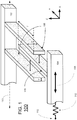
- FIG. 1 shows a drive portion 100 of a MEMS horizontal GCA varactor in accordance with an embodiment of the invention.
- Drive portion 100 includes a drive comb structure 102 having a fixed position and extending along a longitudinal axis 103.
- Drive portion 100 also includes a truss comb structure 104 that extends substantially parallel to axis 103 and that can elastically move along the X direction along a motion axis 105 substantially parallel to axis 103 of drive comb structure 102.
- truss comb structure 104 can include or be attached to at least one restorative or resilient component 110 connected to a fixed end 112.
- the resilient component 110 restores a position of truss comb structure 104 when no external forces are being applied.
- the drive comb structure 102 can have one or more drive fingers 106 extending therefrom towards truss comb structure 104.
- the truss comb structure 104 can similarly include one or more truss fingers 108 extending therefrom towards drive comb structure 102.
- the drive comb structure 102 and the truss comb structure 104 can be positioned to be interdigitating.
- interdigitating refers to arranging comb structure such that the fingers extending from such comb structures at least partially overlap and are substantially parallel.
- fingers 106 and 108 each have a width and a height of a and b , respectively, and overlap of l .
- comb structures with multiple sets of fingers can be configured to have the same dimensional relationships (width, height, and overlap) the invention is not limited in this regard and dimensional relationships can vary, even within a single GCA varactor.
- the portion shown in FIG. 1 and the dimensional relationship shown in FIG. 1 are only the electrically conductive portions of drive portion 100.
- comb structures can further include structural portions comprising non-conductive or semi-conductive materials extending in the Z direction to provide structural support for the conductive portions shown in FIG. 1 . Such structures are more fully described below with respect to FIG. 3 .
- the drive portion 100 shown in FIG. 1 operates on the principle of electrostatic attraction between adjacent interdigitating fingers. That is, motion of the truss comb structure 104 can be generated by developing a voltage difference between the drive comb structure 102 and the truss comb structure 104. In the case of device 100, the voltages applied at comb structures 102 and 104 are also seen at fingers 106 and 108, respectively. The resulting voltage difference generates an attractive force between fingers 106 and fingers 108.
- the electrostatic force between fingers 106 and finger 108 is sufficiently large to overcome the other forces operating on truss comb structure 104 (such as a spring constant of resilient component 110), the electrostatic force will cause the motion of the truss comb structure 104 between a first interdigitated position (resting position at a zero voltage difference) and a second interdigitated position (position at a non-zero voltage difference) among motion axis 105.
- resilient component 110 restores the position of truss comb structure 104 to the first interdigitating position.
- each finger 108 in truss comb structure 104 can be disposed between two fingers 106 of drive comb structure 102. Accordingly, an electrostatic force is generated on both sides of finger 108 when a voltage difference is developed between comb structures 102 and 104. Therefore, to ensure movement of truss comb structure 104 in only one direction in response to a voltage difference, fingers 108 are positioned with respect to fingers 106 such that the electrostatic force in the a first direction along the X-axis is greater than the electrostatic force in an opposite direction in the X-axis.
- the drive portion illustrated in FIG. 1 provides a control mechanism for horizontal actuation in a GCA varactor that can be precisely controlled by adjusting the voltage difference between the drive and truss comb structures. This allows continuous adjustment over a range of interdigitating positions (by adjusting the voltage continuously over a voltage range).
- the drive portion described above could be coupled to any variety of devices, using such a drive portion for various types of devices will only provide a partial improvement in manufacturing robustness and device reliability.
- the robustness of the IC fabrication techniques used for fabricating MEMS devices and other types of devices is increased by reducing the variety of feature types and dimensional variation in each layer.
- the various embodiments of the invention exploit this characteristic.
- another aspect of the invention is to use the comb structure drive portion in conjunction with a comb structure based varactor portion, as shown below in FIG. 2 .
- FIG. 2 shows a top-down view of an exemplary MEMS varactor 200 in accordance with an embodiment of the invention.
- varactor 200 includes a drive portion 201, similar to the drive portion 100 described above with respect to FIG. 1 . That is, drive portion 201 includes a drive comb structures 202a and 202b (collectively 202), a truss comb structure 204, drive fingers 206, and truss fingers 208.
- Truss comb structure 204 also includes resilient portions 210 with fixed ends 212a and 212b (collectively 212).
- resilient portions 210 comprise resilient or flexible reed structures 211 mechanically coupling truss comb structure 204 to fixed ends 212. Therefore, a leaf spring structure is effective formed on the two ends of truss comb structure.
- the reed structures 211 deform to allow truss comb structure to move along motion axis 205 from a first interdigitated position to at least a second interdigitated position.
- the reed structures 211 apply a restorative force to restore the position of the truss comb structure 204 to a first interdigitated position.
- the operation and configuration of components 202-212 is substantially similar to that of components 102-112 in FIG. 1 . Therefore the discussion in FIG. 1 is sufficient for describing the operation and configuration for components 202-210 in FIG. 2 .
- varactor 200 also includes a variable capacitor or varactor portion 214, as shown in FIG. 2 .
- the varactor portion 214 includes input/output comb structures 216a and 216b (collectively 216) having a fixed position.
- the input/output comb structures 216 can also have one or more sense fingers 218 extending therefrom.
- the truss comb structure 204 can additionally include one or more additional truss fingers 220 extending therefrom and interdigitating sense fingers 218. Therefore, the truss comb structure 204 interdigitates (via fingers 208 and fingers 220) both the drive fingers 206 and the sense fingers 218.
- the truss comb structure 204 couples and is part of both the drive portion 201 and the varactor portion 214.
- fingers 206, 208, 218, and 220 are shown to be similarly dimensioned and having a same amount of overlap.
- the invention is not limited in this regard and dimensional relationships can be different in the drive portion 201 and varactor portion 214. Furthermore, the dimensional relationship can also vary within the varactor portion 214.
- the comb structures 202, 204, and 216 can further include conductive portions and structural portions, comprising non-conductive or semi-conductive materials, to provide structure support for the conductive portions. The relationship between these portions will be described below in greater detail with respect to FIG. 3 .
- the varactor 200 is configured to provide functionality as a variable capacitor or varactor.
- the truss comb structure 204 is configured to provide an adjustable capacitance based on adjustment of the gap between a first capacitor plate, provided by fingers 218, and a second capacitor plate, provided by fingers 220. Therefore, varactor 200 forms a first adjustable capacitor or varactor between comb structure 216a and truss comb structure 204, with a capacitance of C OUT1 , and a second adjustable capacitor or varactor between comb structure 216b and truss comb structure 204, with a capacitance of C OUT2 .
- these first and second varactors can be used separately or in combination.
- these varactors can be connected to provide capacitances in series or parallel.
- the capacitance can be measured between comb structures 216a and 216b.
- the capacitance can be measure between comb structures 216a, 216b and fixed end 212a (if electrically coupled to fingers 220).
- a discontinuity 224 is provided to isolate fingers 220 from fingers 208.
- the discontinuity 224 can be provided to reduce any interference between the varactor portion 214 and the drive portion 201. For example, to prevent the charge stored between fingers 218 and 220 from affecting a voltage difference between fingers 206 and 208 and vice versa.
- fixed ends 212a and 212b are both coupled to ground, isolation between drive portion 201 and varactor portion 214 is maintained without requiring such discontinuity 224.
- Varactor 200 operates as follows.
- a circuit (not shown) is coupled to comb structures 216a, 216b, and fixed end 212a (if necessary, as described above).
- V BIAS voltage difference
- a circuit is coupled to comb structures 216a, 216b, and fixed end 212a (if necessary, as described above).
- V BIAS voltage difference
- V BIAS is applied across drive comb structures 202 and fixed end 212b (which is electrically coupled to fingers 208) to cause sufficient electrostatic attraction between fingers 206 and 208 to induce motion of truss comb structure 204, and consequently motion of fingers 220 towards fingers 218, reducing a spacing x 0_CAP between fingers 218 and 220.
- V BIAS is selected to create an electrostatic force that is at least greater than the restorative force of reed structures 211 to cause motion of truss comb structure 204 along motion axis 205.
- V BIAS is reduced such that the electrostatic force is less than the restoring force applied by reed structures 211.
- the restoring force then acts on truss comb structure 204 to increase the gap between fingers 220 from fingers 218, and thus lower the capacitance.
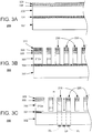
- FIG. 2 can be fabricated using various IC and/or MEMS fabrication techniques. This is illustrated in FIGs. 3A-3C.
- FIGs. 3A-3C show partial cross-sections of device 200 through cutline 3-3 in FIG. 2 during various steps of a fabrication process in accordance with the various embodiments of the invention.
- Manufacture of varactor 200 begins with the formation of the various layers used to form the structures in FIG. 2 . As shown in FIG. 3A , this includes at least one base layer 302, at least one release layer 304 formed on base layer 302, at least one structural layer 306 formed on release layer 304, a lower conductive layer 308, and an upper conductive layer 309 formed on structural layer 306.
- the upper conductive layers 309 can one or more metal layers.
- the lower conductive layers 308 can comprise one or more adhesion layers to improve adhesion between upper conductive layers 309 and structural layer 306. However, in some embodiments, lower conductive layers 308 can be omitted.
- the materials for layers 304-309 can be formed on base layer 302 in a variety of ways, including thermal oxidation, physical/chemical deposition, sputtering, and/or electroplating processes, depending on the type and composition of the layer being formed.
- the composition of structural layer 306 is selected such that it is electrically non-conductive.
- the composition of release layer 304 is selected such that it can be selectively removable, with respect to base layer 302, structural layer 306, and conductive layers 308, 309, using at least one removal process.
- layers 302-306 are provided by using a silicon on insulator (SOI) substrate. In such a substrate, the silicon oxide comprising layer sandwiched between two layers of silicon provides release layer 304 between the silicon-comprising base layer 302 and structural layer 306.
- SOI silicon on insulator
- the invention is not limited to SOI substrates.
- the release layer 304 and structural layer 306 are formed on a silicon substrate that provides base layer 302.
- non-silicon comprising materials are used for forming layers 302-306.
- the structures shown in FIG. 3B for device 200 are formed by creating voids in conducting layers 308, 309, structural layer 306, and release layer 304. This step can be performed in a variety of ways.
- a masking layer 310 can be formed on layer 309, having a mask pattern in accordance with the structures in device 200.
- the portion of masking layer 310 shown in FIG. 3B shows the mask pattern for portions of reed structure 211, fixed end 212a, fingers 218, and fingers 220.
- various dry and/or wet etching processes are used to transfer the mask pattern into conducting layers 308, 309 and structural layer 306.
- the exemplary mask pattern shown in FIG. 3B provides for the same pattern to be transferred into both conducting layers 308, 309 and structural layer 306, the various embodiments of the invention are not limited in this regard.
- two masking steps are performed. For example, a first mask pattern can be provided for etching conducting layers 308. Afterwards a second mask pattern is provided for etching structural layer 306.
- portions of release layer 304 are removed to "release" at least some portions of truss comb structure 204. This can be accomplished by providing an isotropic selective removal process to device 200. An isotropic process not only removes the exposed portions of release layer 304, but will also removes portions of release layer 304 (i.e., creates voids) beneath structural layer 306 in the vicinity of openings in structural layer 306 (i.e., undercut these structures). If the lateral dimensions of features in structural layer 304 are small enough (such as under reed structures 211, fingers 218, and fingers 220 shown in FIGs. 3A-C ), all portions of the release layer 304 underneath such features will be removed.
- such features can be realized by utilizing an SOI substrate and a hydrofluoric (HF) acid-based etch. First an etch process is used to form the voids shown in FIG. 3B . Afterwards, an HF acid-based etch process is used to selectively remove and undercut portions of the silicon oxide comprising layer, creating voids beneath selected features of device 200, to result in the structure shown in FIG. 3C .
- HF hydrofluoric
- ALE atomic layer epitaxial
- the process flow described above in FIGs. 3A-3C can be used to form the varactor illustrated in FIG. 2
- one limitation of this process flow and similar process flows is that it can be difficult to fabricate such a device and match desired dimension accurately.
- several of the processing steps described above can give rise to errors in the dimensions of the drive comb structures 202, input/output comb structures 216, and the movable truss 204.
- the various masking and etching steps can result in variations in the dimensions of fingers 206, 208, 218, and 220.
- the wet etching steps such as the HF etch process described above, are generally difficult to control and can result in overetching of the resulting features.
- capacitor plate areas i.e., the heights (H) and lengths (not shown) of fingers 206, 208, 218, 220
- the widths e.g., W1 and W2
- the spacings SP
- Such variation is generally inherent in most types of varactor devices. That is, the manufacture of varactor devices of any type generally introduces some variation in the dimensions of the device. As a result, it is generally difficult to provide a varactor device that provides capacitance values accurately.
- One solution is to calibrate such devices. Thus, the appropriate values of V BIAS for target capacitance values can be determined prior to use. However, such a solution generally results in additional procedures being needed to install and use the varactor device. For example, the system utilizing the device would also need to be calibrated or adjusted to account for the variation in the varactor device being installed.
- Another solution is to monitor the capacitance value during use and provide adjustments during use. However, such a configuration results in at least some of the charge of the capacitor being diverted to sensing devices.
- a second, separate monitoring capacitor could be used to estimate the behavior of a first active capacitor of a circuit.
- the monitoring capacitor may not accurately reflect the resulting structure of the active capacitor.
- variations in wiring and contact resistances can result in different input signals being provided to the monitoring capacitor.
- the operation and resulting behavior of the monitoring capacitor may not accurately reflect the operation and behavior of the active capacitor.
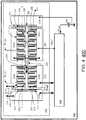
- another aspect of the invention provides for fabricating high accuracy varactor devices by combining GCA varactor devices, as shown in FIG. 2 , with a feedback circuit.
- the different comb structures of a single GCA varactor device are used to provide an output varactor portion and a reference varactor portion.
- the feedback circuit can be used to monitor the reference varactor portion and adjust the value of V BIAS provided to the GCA varactor device. Such a configuration is illustrated below in FIG. 4 .
- FIG. 4 shows a schematic of a MEMS varactor device 400 in accordance with an embodiment of the invention.
- device 400 includes GCA varactor 200 coupled to a feedback circuit 404.
- the GCA varactor 200 and the feedback circuit 404 can be formed on a same supporting structure 406, as shown in FIG. 4 .
- supporting structure 406 can be a substrate and the GCA varactor 200 and the feedback circuit 404 can be formed thereon using various IC and MEMS fabrication techniques.
- the GCA varactor 200 and the feedback circuit 404 can be formed on different supporting substrates and afterwards combined using conventional methods. Such methods can include system-in-a-package and/or printed circuit board (PCB) fabrication methods.
- PCB printed circuit board
- the GCA varactor 200 is configured similarly to the GCA varactor described above in FIG. 2 . That is, the GCA varactor 200 includes a drive portion 201 similar to that of FIG. 2 . Accordingly, the description provided above for FIG. 2 is sufficient for describing the structure and operation of components 202a, 202b, 204, 206, 207, 208, 210, 211, 212a, and 212b in FIG. 4 . In addition to drive portion 201, the GCA varactor 200 also includes a varactor portion 214 similar to the varactor portion of FIG. 2 . Accordingly, the description provided above for FIG. 2 is sufficient for describing the structure and operation of components 216a, 216b, 218, and 220 in FIG. 4 .
- GCA varactor 200 provides first and second variable capacitors or varactors, C OUT1 and C OUT2 .
- C OUT2 can be used as a reference varactor for monitoring and accurately adjusting the C OUT1 .
- Such a configuration is more accurate for estimating the capacitance value of C OUT1 , as compared to conventional methods, for at least two reasons.
- the capacitance values of C OUT1 and C OUT2 vary due to the same action. That is, instead of adjusting the capacitance of a reference varactor using a portion of a bias signal or a different signal related the bias signal, a same signal independently and simultaneously adjusts both the output and reference varactors. For example, in FIG.
- the bias voltage applied to the drive portion 201 causes the motion of the movable truss 204, which simultaneously changes the capacitance of both C OUT1 and C OUT2 .
- any variations between the reference and output varactors that are normally caused by differences in wiring, contact resistance, and other signaling differences are effectively eliminated.
- the electrical operation of C OUT1 is not significantly affected by the electrical operation of C OUT2 .
- the comb structures 216a and 216b and the movable truss 204 are simultaneously fabricated in the same device, process bias-induced variations in the reference varactor are substantially reduced. In particular, global manufacturing variations are irrelevant since the reference varactor and the output varactor are part of the same device.
- C OUT2 will generally substantially track with the capacitance values provided by C OUT1 .
- C OUT2 can be monitored and used to accurately determine any adjustment in bias voltage needed to provide a target output capacitance value at C OUT1 .
- device 400 provides feedback circuit 404 for monitoring C OUT2 and modifying V BIAS to provide a V BIAS ' to provide the output capacitance target at C OUT1 associated with a selected V BIAS .
- voltage source 418 is illustrated as a battery in the exemplary embodiments illustrated herein, the invention is not limited in this regard. In the various embodiments of the invention, voltage source 418 can be a variable voltage source receiving a control signal from one or more components on substrate 406, such as feedback circuit 404 or a separate controller circuit, or from one or more components located elsewhere.
- the feedback circuit 404 determines an amount of voltage adjustment for V BIAS based on the capacitance at C OUT2 . That is, feedback circuit determines the amount of voltage adjustment need for the capacitance at C OUT2 to provide a target C OUT2 capacitance associated with V BIAS . Feedback circuit 404 then adjusts V BIAS by the voltage adjustment amount to obtain a voltage V BIAS '. V BIAS ' is then provided to the drive portion 201 to adjust the position of movable truss 204 beyond that provided by V BIAS alone. As a result, the capacitance values at C OUT1 and C OUT2 are adjusted. The process can then be repeated until C OUT2 is at the capacitance value corresponding to the target capacitance value for C OUT2 corresponding to a target capacitance value for C OUT1 for the selected V BIAS .
- feedback circuit 404 can be configured using analog circuit elements, digital circuit elements, or a combination of both. Accordingly, one of ordinary skill in the art will recognize that the feedback circuit 404 can be implemented in a variety of ways.
- feedback circuit 404 can be a digital controller circuit that accepts V BIAS , a capacitance value of C OUT2 and that automatically computes or looks up a V BIAS ' value for adjusting the capacitance value of C OUT2 to a value associated with a target C OUT1 .
- a feedback circuit 404 can be fabricated using solely analog circuits. One such configuration will be described below in greater detail with respect to FIGs. 6-10 .
- a larger capacitance may be needed than can be provided by the combination of comb structure 216a and movable truss 204 providing C OUT1 .
- One solution is to increase the number of fingers to increase the capacitance values for C OUT1 .
- the maximum capacitance will limited by manufacturing tolerances. That is, in any MEMS manufacturing process, there will be a minimum line width and line spacing that is achievable. However, such minimum line widths and spacing may be undesirable since the resulting structures may be too thin or fragile to support themselves. Accordingly, it can be necessary to increase the area occupied by GCA varactor to accommodate an additional number of fingers.
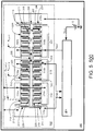
- FIG. 5 shows a schematic of another MEMS varactor device 500 in accordance with an embodiment of the invention.
- device 500 also includes a GCA varactor 502 and a feedback circuit 404 which can be optionally formed on a same supporting structure 406.
- GCA varactor 502 is also configured similarly to the GCA varactor described above in FIG. 2 . That is, the GCA varactor 502 also includes a drive portion 201, similar to the drive portion of FIG. 2 . Accordingly, the description provided above for FIG. 2 is sufficient for describing the structure and operation of components 202a, 202b, 204, 206, 207, 208, 210, 211, 212a, and 212b in FIG. 5 .
- the GCA varactor 200 also includes a first varactor portion 214 for providing an output capacitance C OUT using a parallel combination of C OUT1 and C OUT2 , as shown in FIG. 5 . This first varactor portion 214 is similar to the varactor portion of FIG.
- FIG. 2 Accordingly, the description provided above for FIG. 2 is sufficient for describing the structure and operation of components 216a, 216b, 218, and 220 in FIG. 5 . Additionally, a relatively large output capacitance value is provided by coupling the varactor formed by comb structure 216a and movable truss 204 and the varactor formed by comb structure 216b and movable truss 204 in parallel.
- GCA varactor 502 also includes a second varactor portion 514 for providing the reference capacitance C REF , as shown in FIG. 5 .
- the second varactor portion 514 is also configured similarly to the varactor portion of FIG. 2 . Accordingly, the description provided above for the varactor portion of FIG. 2 is also sufficient for describing the structure and operation of components 516a, 516b, 518, and 520 in FIG. 5 .
- first varactor portion 214 and second varactor portion 514 are shown as being similarly configured. That is, first varactor portion 214 and second varactor portion 514 are shown as including a similar number of fingers and in which the dimensions of the fingers are similar. However, the invention is not limited in this regard. In some embodiments of the invention, the dimensions of the fingers and the spacings can be different for varactor portion 214 as compared to varactor portion 514. Therefore, the first varactor portion 214 and the second varactor portion 514 can provide different capacitance values in other embodiments of the invention.
- the first varactor portion 214 can be configured to have a large number of fingers 218, 220 to provide a relatively high capacitance.
- the second varactor portion 514 can be configured to have a smaller number of fingers 518, 520, as compared to varactor portion 214, to provide a relatively lower capacitance.
- the reference capacitance value can be provided by coupling the varactor formed by comb structure 516a and movable truss 204 and the varactor formed by comb structure 516b and movable truss 204 in parallel, as shown in FIG. 5 . This allows the area needed for second varactor portion 514 to be reduced further. As a result, a majority of the area of GCA varactor 502 associated with varactor structures can be occupied by the varactor structures for providing the output capacitance of GCA varactor 502.
- GCA varactor 502 operates as follows. To increase the amount of capacitance provided by both the first varactor portion 214 and the second varactor portion 514, a voltage difference (V BIAS ) is developed between fingers 206 and 208 to generate electrostatic attraction between these fingers. For example, as shown in FIG. 5 , V BIAS ' is applied across drive comb structures 202 and fixed end 212b (which is electrically coupled to fingers 208) to cause sufficient electrostatic attraction between fingers 206 and 208 to induce motion of truss comb structure 204 along motion axis 205 and reduce x 0_DRV . The motion of truss comb structure 204 consequently causes the simultaneous motion of fingers 220 towards fingers 218 and fingers 520 towards fingers 518.
- V BIAS voltage difference
- the spacing x 0_CAP_A between fingers 218 and 220 is reduced and the spacing x 0_CAP_B between fingers 518 and 520 is also reduced. Consequently, the reduction of these spacings also reduces the spacing between the capacitor plates in varactor portions 214 and 514, resulting in a change of the capacitance values provided by varactor portions 214 and 514.
- the varactor portion 514 can be used as a reference varactor for monitoring and accurately adjusting the output capacitance of varactor portion 214 using feedback circuit 404, as described above with respect to FIG. 4 . Accordingly, the description provided above for the device in FIG. 4 is also sufficient for describing the structure and operation of feedback circuit 404.
- the feedback circuit 404 in FIGs. 4 and 5 is used to modify a bias voltage provided by bias source 418 (V BIAS ) in order to provide a VBIAS' that results in the target output capacitance value associated with V BIAS .
- V BIAS bias source 418
- the feedback circuit 404 in FIGs. 4 and 5 can be implemented in a variety of ways. For example, one exemplary implementation is described below with respect to FIG. 6.
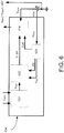
- FIG. 6 shows a detailed schematic illustration of one exemplary configuration for the feedback circuit 404 in a MEMS varactor device in accordance with an embodiment of the invention.
- the configuration of the feedback circuit 404 includes a converter element 620 for performing a conversion step, a comparison element 622 for performing a comparison step, and a voltage adjusting element 624 for performing a voltage adjustment step.
- the feedback circuit 404 can also include a controller element 626. Although various blocks are shown in FIG. 6 , one of ordinary skill in the art will readily recognize that any of the blocks shown in FIG. 6 can be combined.
- the exemplary feedback circuit 404 in FIG. 6 operates as follows. First, C REF is converted to a voltage V REF using converter element 620, as described below with respect to FIGs. 7 and 8 . Second, V REF is compared to a set point voltage V SP using a comparison element 622. In some embodiments, the controller element 626 can supply V SP . In such a configuration, controller element 626 can receive V BIAS and automatically determine V SP using computational or lookup methods. However, the various embodiments of the invention are not limited in this regard and V SP can also be supplied by circuits external to feedback circuit 404.
- comparison element 622 Based on this comparison, comparison element 622 generates an output signal comprising 0V (indicating that no change is needed) or an incrementing voltage ⁇ V (indicating that a change is needed).
- An exemplary configuration for a comparison element will be described below in further detail with respect to FIG. 9 .
- the comparison element 622 continues to generate an output signal comprising an incrementing voltage ⁇ V until V REF is less than or equal to V SP .
- the reference varactor is assumed to be providing a capacitance value C REF corresponding to a target capacitance value C OUT for the output varactor. Accordingly, no further adjustment of V BIAS would be needed.
- the voltage adjusting element 624 will continue accumulate a sum of ⁇ V over time and add this sum to V BIAS to produce an adjusted bias voltage V BIAS '.
- the feedback circuit 404 in FIG. 6 first performs a conversion step to convert the reference capacitance obtained from GCA varactor in FIGs. 4 or 5 to a reference voltage V REF .
- a conversion step is used since comparison of capacitance values is generally non-trivial.
- conversion of a capacitance value to a voltage and comparison of voltages is relatively straightforward to implement. Accordingly, by converting the reference capacitance C REF to a reference voltage V REF , the circuit configuration needed for making an adjustment to V BIAS is greatly simplified.
- An exemplary configuration for convertor circuit 620 shown in FIG. 7 An exemplary configuration for convertor circuit 620 shown in FIG. 7 .
- the various embodiments of the invention are not limited in this regard and other circuits can be provided for converting the reference capacitance to a reference voltage.
- FIG. 7 shows an exemplary configuration for the converter element 620 in accordance with an embodiment of the invention.
- the converter element 620 can include a resistance-capacitance (RC) filter 702 and an envelope detector 704.
- the RC filter 702 receives a square wave input waveform S 1 and generates a time-varying output waveform S 2 , where S 2 varies according to variations in C REF .
- Envelope detector 704 then generates V REF based on waveform S 2 .
- waveform S 1 can be generated within converter element 620, using a square wave generator 706.
- waveform S 1 can be provided from a square wave generator operating external to converter element 620.
- any type of square wave generator can be used to provide S 1 .
- the design and fabrication of stand-alone and integrated square wave generators is well known to those of ordinary skill in the art and will not be described herein.
- an RC filter 702 is employed to generate waveform S 2 from waveform S 1 .
- RC filter 702 can be configured in a variety of ways.
- FIG. 8 shows a schematic illustration of an exemplary configuration for RC filter 702 in accordance with an embodiment of the invention.
- RC filter 702 is configured as a low pass filter.
- a resistor R and the reference capacitance C REF are arranged in series with a source of waveform S 1 and the voltage measured across C REF is used as waveform S 2 . Therefore, as the value of C REF varies over time, the voltage or potential divider in RC filter 704 also changes over time.
- the variation in C REF results in a variable impedance that generally varies inversely proportional to C REF , assuming that the frequency of S 1 is constant. Consequently, as C REF is increased over time, the variable impedance is also decreased. As a result, the voltage across C REF is also decreased over time and the waveform S 2 will also vary over time. In particular, the decreasing voltage across C REF will decrease the amplitude of S 2 . Thus, the waveform S 2 provides a waveform with an amplitude inversely indicative of the current value of C REF .
- envelope detector 704. In the various embodiments of the invention, any type of envelope detector circuit can be used. Such circuits are well known to those of ordinary skill in the art and will not be described herein.
- Envelope detector 704 is used to measure or detect the varying amplitude of the waveform S 2 due to the variations in C REF . As a result, a value for V REF is generated, where V REF is a voltage signal that varies over time based on the variation in the amplitude of S 2 caused by the variation in C REF . Accordingly, such a signal can then be used in a subsequent comparison step to determine if adjustment of V BIAS is needed.
- the reference voltage generated during the conversion step in converter element 620 can then be compared to a set point voltage V SP in a comparison element 622 to generate a signal that can be used during a subsequent voltage adjusting step to adjust the value of V BIAS . Based on this signal, the adjustment step can be performed to adjust operation of the GCA varactor and thus the output capacitance.
- One exemplary configuration for comparison element 622 is shown in FIG. 9 .
- FIG. 9 shows a schematic illustration of an exemplary configuration for a comparison element 622 for the feedback circuit 404 in FIG. 6 .
- the comparison element 622 can be provided using an operational amplifier (op-amp) comparator circuit, such as that as shown in FIG. 9 .
- an op-amp circuit is illustrated including an op-amp comparator 902 with an output pull-up resistor RL.
- the non-inverting input (+) of op-amp 902 can be configured to receive V REF and the inverting input (-) of op-amp 902 can be configured to receive V SP .
- the pull-up resistor can be connected to an incrementing voltage ⁇ V.
- V REF if V REF is greater than V SP , the comparator element 822 outputs ⁇ V. In contrast, if V REF is less than V SP , the comparator element 822 outputs 0V.
- V REF if V REF is greater than V SP , the comparator element 822 outputs 0V.
- the various embodiments of the invention are not limited to the configuration illustrated in FIG. 9 . Rather, any type of comparator element configuration for generating an output signal of 0V or ⁇ V based on a comparison of V REF and V SP can be used in the various embodiments of the invention.
- FIG. 10 shows an exemplary configuration for the voltage adjusting element 624 of the feedback circuit 404 in FIG. 6 .
- the voltage adjusting element 624 includes an accumulator circuit 1000, including a gated voltage latch circuit 1002 and a first summing voltage circuit 1004.
- the term "gated voltage latch circuit”, as used herein, refers to any type of circuit that can store a voltage level based on an enable signal. That is, a new voltage level cannot be stored in the circuit until an enable signal is received. In the various embodiments of the invention, any type of gated latch circuits can be used.
- the latch circuit 1002 can comprise a row of resistors increasing or decreasing in value and receiving V SUM . These resistors would individually be connected to gated SR latches (clocked SR flip-flops). These SR flip-flops would then be connected back together to a summer circuit to provide a summed output for V STORED .
- V SUM the number of SR latches turn on also increases, based on the resistor values.
- the SR latches are gated, the value for V STORED would only change based on the clock signal.
- Feedback circuit 624 also includes a second summing voltage circuit 1006.
- the term "summing voltage circuit”, as used herein, refers to any circuit capable of receiving at least two voltage signals and outputting a signal having a voltage equal to the sum of the received voltage signals. Such circuits are well known to those of ordinary skill in the art and will not be described herein.
- Voltage adjusting circuit 624 operates as follows. Initially, the latch 1002 in accumulator circuit 1000 is configured to store a voltage V STORED equal to 0V. Thereafter, during a first clock cycle, latch 1002 outputs V STORED to summing circuit 1004 in accumulator circuit 1000. However, latch 1002 will not be enabled to store a new value for V STORED . Summing circuit 1004 also receives an output of comparison element 622, comprising 0V or an incrementing voltage ⁇ V. As a result, summing circuit 1004 generates a sum voltage V SUM comprising the sum of V STORED and one of 0V or an incrementing voltage ⁇ V provided by comparison element 622.
- V SUM will equal to 0V or ⁇ V.
- the clock signal CLK enables latch 1002 to store the V SUM as V STORED .
- values of ⁇ V are accumulated over time. That is, V STORED is increased in increments of ⁇ V.
- the voltage V SUM will be equal to n ⁇ V over time, where n is an integer greater than 0.
- signal CLK can be provided by controller 626, as shown in FIG. 6 .
- signal CLK can be supplied by one or more external components.
- V SUM is passed to summing circuit 1006.
- Summing circuit 1006 also receives the bias voltage V BIAS from bias source 418. Summing circuit 1006 then generates a sum voltage V BIAS ' equal to V SUM + V BIAS . The sum voltage V BIAS ' is then provided to the drive portion of the GCA varactor. Over time, the voltage adjusting circuit 624 continues to increase V BIAS ' as long V SUM is continued to be increased. Accordingly, once comparison element 622 ceases to output ⁇ V, no further changes to V SUM are provided, indicating that the output capacitance C OUT is at a target value.
Landscapes
- Engineering & Computer Science (AREA)
- Power Engineering (AREA)
- Microelectronics & Electronic Packaging (AREA)
- Micromachines (AREA)
Claims (10)
- System umfassend ein Kapazitätsdioden-Gerät, das Kapazitätsdioden-Gerät umfassend:eine Lücken schließende Aktuator (GCA)-Kapazitätsdiode (200, 502), umfassend wenigstens eine Kammantriebsstruktur (202), wenigstens eine Ausgangs-Kapazitätsdioden-Struktur (214, 216a), die eine Ausgangskapazität (COUT, COUT1) definiert, wenigstens eine Referenz-Kapazitätsdioden-Struktur (214, 216b), die eine Referenzkapazität (CREF, COUT2) definiert, und wenigstens eine bewegliche Trägerkammstruktur (204), die mit der Kammantriebsstruktur (202), der Ausgangs-Kapazitätsdiode, und den Referenz-Kapazitätsdioden-Strukturen ineinandergreift, wobei die Trägerkammstruktur dazu ausgebildet ist, sich entlang einer Bewegungsachse (105) zwischen einer Vielzahl von interdigitalen Positionen basierend auf einer Ausgangsvorspannung zu bewegen, die auf die Trägerkammstruktur und die Kammantriebsstruktur (202) angewendet wurde;einen Rückführkreis (404), der elektrisch zu der Referenz-Kapazitätsdioden-Struktur gekoppelt ist, wobei der Rückführkreis (404) zum selektiven Modifizieren einer Eingangsvorspannung (VBIAS) basierend auf der Referenzkapazität (CREF, COUT2) ausgebildet ist, um die Ausgangsvorspannung (VBIAS') zu erzeugen, die eine Zielkapazität bei der Ausgangs-Kapazitätsdioden-Struktur (214, 216a) bereitstellt.
- System nach Anspruch 1, wobei der Rückführkreis (404) ein Umwandlerelement (620) zum Erzeugen einer Referenzspannung (VREF) basierend auf der Referenzkapazität (CREF, COUT2), ein Vergleicherelement (622) zum Vergleichen der Referenzspannung (VREF) zu einer gesetzten Punktspannung (VSP), und ein Spannungsanapassungselement (624) zum Erzeugen der Ausgangsvorspannung basierend auf einer Eingangsvorspannung und einem Vergleichsausgang des Vergleicherelements (622) umfasst.
- System nach Anspruch 2, wobei der Rückführkreis (404) weiter wenigstens ein Steuerelement (626) zum Erzeugen wenigstens eines der Eingangsvorspannung (VBIAS) und der gesetzten Punktspannung (VSP) umfasst.
- System nach Anspruch 2, wobei das Vergleicherelement (622) einen Spannungsvergleicherkreis (902) umfasst, der zum Vergleichen der gesetzten Punktspannung (VBIAS) und der Referenzspannung (VREF) und zum Erzeugen des Vergleichsausgangs basierend auf dem Vergleich ausgebildet ist.
- System nach Anspruch 4, wobei der Spannungsvergleicherkreis (902) dazu ausgebildet ist, den Vergleichsausgang als inkrementierende Spannung auszugeben, wenn die Referenzspannung (VREF) größer als die gesetzte Punktspannung (VSP) ist, und den Vergleichsausgang als eine Grundspannung auszugeben, wenn die Referenzspannung (VREF) kleiner als die gesetzte Spannung (VSP) ist.
- System nach Anspruch 4, wobei das Spannungsanpassungselement (624) einen Akkukreis (1000) umfasst, der zu einem ersten summierenden kreis (1004) gekoppelt ist, wobei der Akkukreis (1000) dazu ausgebildet ist, den Vergleichsausgang über Zeit aufzusummieren, um eine Anpassungsspannung zu erzeugen, und der erste summierende Kreis (1004) dazu ausgebildet ist, die Ausgangsvorspannung durch Addieren der Anpassungsspannung zu der Eingangsvorspannung zu erzeugen.
- Verfahren zum Anwenden einer Lücken schließenden Aktuator (GCA)-Kapazitätsdiode (200, 502), umfassend wenigstens eine Kammantriebsstruktur (202), wenigstens eine Ausgangs-Kapazitätsdioden-Struktur (214, 216a), die eine Ausgangskapazität (COUT, COUT1) definiert, wenigstens eine Referenz-Kapazitätsdioden-Struktur (214, 216b), die eine Referenzkapazität (CREF, COUT2) definiert, und wenigstens eine bewegliche Trägerkammstruktur (204), die mit der Kammantriebsstruktur (202), der Ausgangs-Kapazitätsdiode, und den Referenz-Kapazitätsdioden-Strukturen ineinandergreift, wobei die Trägerkammstruktur dazu ausgebildet ist, sich entlang einer Bewegungsachse (105) zwischen einer Vielzahl von interdigitalen Positionen basierend auf einer Ausgangsvorspannung zu bewegen, die auf die Trägerkammstruktur und die Kammantriebsstruktur (202) angewendet wurde, das Verfahren umfassend:Bereitstellen einer Eingangsvorspannung (VBIAS) für die Kammantriebsstruktur (202); undModifizieren der Eingangsspannung (VBIAS) basierend auf der Referenzkapazität (CREF, COUT2), um die Ausgangsvorspannung zu erzeugen, die eine Zielkapazität bei der Ausgangs-Kapazitätsdioden-Struktur bereitstellt.
- Verfahren nach Anspruch 7, weiter umfassend:Auswählen eines Initialwerts für die Ausgangsvorspannung (VBIAS') durch Verwenden einer Eingangsvorspannung (VBIAS), die mit einer Zielkapazität für die Ausgangskapazität (COUT; COUT1) verbunden ist;Erhalten einer Referenzspannung (VREF) basierend auf einem Wert der Referenzkapazität, die sich aus dem Initialwert der Ausgangsvorspannung ergibt;Vergleichen der Referenzspannung (VREF) zu einer gesetzten Punktspannung (VSP), die mit der Zielkapazität verbunden ist; undAnpassen der Ausgangsvorspannung (VBIAS') basierend auf dem Vergleichen, um eine Differenz zwischen der Referenzspannung (VREF) und der gesetzten Punktspannung (VSP) zu reduzieren.
- Verfahren nach Anspruch 7, wobei das Vergleichen weiter umfasst:Vergleichen der gesetzten Punktspannung (VSP) zu der Referenzspannung (VREF);Ausgeben, als den Vergleichsausgang, eine inkrementierende Spannung, wenn die Referenzspannung (VREF) kleiner als die gesetzte Punktspannung (VSP) ist; undAusgeben, als den Vergleichsausgang, einer Grundspannung, wenn die Referenzspannung (VREF) größer als die gesetzte Punktspannung (VSP) ist.
- Verfahren nach Anspruch 7, wobei das Anpassen weiter umfasst:Summieren des Vergleichsausgangs über Zeit, um eine nächste Anpassungsspannung zu erzeugen, undAusgeben einer Summe der nächsten Anpassungsspannung und der Eingangsvorspannung als die Ausgangsvorspannung.
Applications Claiming Priority (2)
| Application Number | Priority Date | Filing Date | Title |
|---|---|---|---|
| US12/699,118 US8373522B2 (en) | 2010-02-03 | 2010-02-03 | High accuracy MEMS-based varactors |
| PCT/US2011/022483 WO2011097093A2 (en) | 2010-02-03 | 2011-01-26 | High accuracy mems-based varactors |
Publications (2)
| Publication Number | Publication Date |
|---|---|
| EP2532017A2 EP2532017A2 (de) | 2012-12-12 |
| EP2532017B1 true EP2532017B1 (de) | 2018-05-23 |
Family
ID=44341475
Family Applications (1)
| Application Number | Title | Priority Date | Filing Date |
|---|---|---|---|
| EP11703322.5A Active EP2532017B1 (de) | 2010-02-03 | 2011-01-26 | Hochpräzise mems-basierte varaktoren |
Country Status (7)
| Country | Link |
|---|---|
| US (1) | US8373522B2 (de) |
| EP (1) | EP2532017B1 (de) |
| JP (1) | JP2013519230A (de) |
| KR (1) | KR101328905B1 (de) |
| CA (1) | CA2788586C (de) |
| TW (1) | TWI437594B (de) |
| WO (1) | WO2011097093A2 (de) |
Cited By (1)
| Publication number | Priority date | Publication date | Assignee | Title |
|---|---|---|---|---|
| DE102021204653A1 (de) | 2021-05-07 | 2022-11-10 | Fraunhofer-Gesellschaft zur Förderung der angewandten Forschung e.V. | In-plane MEMS-Varaktor |
Families Citing this family (11)
| Publication number | Priority date | Publication date | Assignee | Title |
|---|---|---|---|---|
| US9293521B2 (en) | 2012-03-02 | 2016-03-22 | Taiwan Semiconductor Manufacturing Co., Ltd. | Concentric capacitor structure |
| US8860114B2 (en) * | 2012-03-02 | 2014-10-14 | Taiwan Semiconductor Manufacturing Company, Ltd. | Structure and method for a fishbone differential capacitor |
| US9185820B2 (en) | 2012-12-11 | 2015-11-10 | Harris Corporation | Monolithically integrated RF system and method of making same |
| US9093975B2 (en) | 2013-08-19 | 2015-07-28 | Harris Corporation | Microelectromechanical systems comprising differential inductors and methods for making the same |
| US9172352B2 (en) | 2013-08-19 | 2015-10-27 | Harris Corporation | Integrated microelectromechanical system devices and methods for making the same |
| US9136822B2 (en) | 2013-08-19 | 2015-09-15 | Harris Corporation | Microelectromechanical system with a micro-scale spring suspension system and methods for making the same |
| US9123493B2 (en) * | 2014-01-23 | 2015-09-01 | Harris Corporation | Microelectromechanical switches for steering of RF signals |
| DE102014210747B4 (de) | 2014-02-12 | 2023-11-16 | Rohde & Schwarz GmbH & Co. Kommanditgesellschaft | Phasenregelschleife mit Varaktor in Mikrosystemtechnik |
| DE102014002823B4 (de) * | 2014-02-25 | 2017-11-02 | Northrop Grumman Litef Gmbh | Mikromechanisches bauteil mit geteilter, galvanisch isolierter aktiver struktur und verfahren zum betreiben eines solchen bauteils |
| FR3067853A1 (fr) * | 2017-06-15 | 2018-12-21 | Commissariat A L'energie Atomique Et Aux Energies Alternatives | Condensateur a capacite variable electromecanique a quatre electrodes |
| CN113707457A (zh) * | 2021-07-20 | 2021-11-26 | 国网江苏省电力有限公司连云港市赣榆区供电分公司 | 一种距离控制型可调容量高压电容器 |
Family Cites Families (40)
| Publication number | Priority date | Publication date | Assignee | Title |
|---|---|---|---|---|
| US5025346A (en) | 1989-02-17 | 1991-06-18 | Regents Of The University Of California | Laterally driven resonant microstructures |
| JPH08181038A (ja) * | 1994-12-26 | 1996-07-12 | Murata Mfg Co Ltd | 可変容量コンデンサ |
| US5640133A (en) * | 1995-06-23 | 1997-06-17 | Cornell Research Foundation, Inc. | Capacitance based tunable micromechanical resonators |
| US5959516A (en) | 1998-01-08 | 1999-09-28 | Rockwell Science Center, Llc | Tunable-trimmable micro electro mechanical system (MEMS) capacitor |
| CA2352166A1 (en) | 1998-12-11 | 2000-06-15 | Paratek Microwave, Inc. | Electrically tunable filters with dielectric varactors |
| US6566786B2 (en) | 1999-01-14 | 2003-05-20 | The Regents Of The University Of Michigan | Method and apparatus for selecting at least one desired channel utilizing a bank of vibrating micromechanical apparatus |
| US6497141B1 (en) | 1999-06-07 | 2002-12-24 | Cornell Research Foundation Inc. | Parametric resonance in microelectromechanical structures |
| US6133670A (en) | 1999-06-24 | 2000-10-17 | Sandia Corporation | Compact electrostatic comb actuator |
| KR100344790B1 (ko) | 1999-10-07 | 2002-07-19 | 엘지전자주식회사 | 마이크로 기계구조를 이용한 주파수 가변 초고주파 필터 |
| KR100312432B1 (ko) | 1999-11-25 | 2001-11-05 | 오길록 | 마이크로 구조체를 이용한 광스위치 |
| US6621390B2 (en) | 2001-02-28 | 2003-09-16 | Samsung Electronics Co., Ltd. | Electrostatically-actuated capacitive MEMS (micro electro mechanical system) switch |
| US6771001B2 (en) | 2001-03-16 | 2004-08-03 | Optical Coating Laboratory, Inc. | Bi-stable electrostatic comb drive with automatic braking |
| US7091647B2 (en) | 2001-07-31 | 2006-08-15 | Coherent, Inc. | Micromechanical device having braking mechanism |
| US6982515B2 (en) | 2001-09-12 | 2006-01-03 | Brigham Young University | Dual position linear displacement micromechanism |
| DE10148858A1 (de) * | 2001-10-04 | 2003-04-10 | Bosch Gmbh Robert | Mikromechanischer Sensor mit Selbsttestfunktion und Optimierungsverfahren |
| US6798315B2 (en) | 2001-12-04 | 2004-09-28 | Mayo Foundation For Medical Education And Research | Lateral motion MEMS Switch |
| US6611168B1 (en) | 2001-12-19 | 2003-08-26 | Analog Devices, Inc. | Differential parametric amplifier with physically-coupled electrically-isolated micromachined structures |
| US6917268B2 (en) | 2001-12-31 | 2005-07-12 | International Business Machines Corporation | Lateral microelectromechanical system switch |
| US6784766B2 (en) | 2002-08-21 | 2004-08-31 | Raytheon Company | MEMS tunable filters |
| US6661069B1 (en) | 2002-10-22 | 2003-12-09 | International Business Machines Corporation | Micro-electromechanical varactor with enhanced tuning range |
| JP2004286615A (ja) * | 2003-03-24 | 2004-10-14 | Denso Corp | 半導体加速度センサ |
| US6975193B2 (en) | 2003-03-25 | 2005-12-13 | Rockwell Automation Technologies, Inc. | Microelectromechanical isolating circuit |
| US7190245B2 (en) | 2003-04-29 | 2007-03-13 | Medtronic, Inc. | Multi-stable micro electromechanical switches and methods of fabricating same |
| US6853534B2 (en) | 2003-06-09 | 2005-02-08 | Agilent Technologies, Inc. | Tunable capacitor |
| US7304556B2 (en) | 2003-08-11 | 2007-12-04 | Murata Manufacturing Co., Ltd. | Buckling actuator |
| CN1842885B (zh) | 2003-08-26 | 2011-08-03 | 松下电工株式会社 | 静电驱动可锁止致动器系统 |
| KR20060094525A (ko) * | 2003-10-20 | 2006-08-29 | 유니버시티오브데이턴 | 용량성 분기 스위칭에 적절한 강유전체 바랙터 |
| US7265019B2 (en) | 2004-06-30 | 2007-09-04 | International Business Machines Corporation | Elastomeric CMOS based micro electromechanical varactor |
| US7251466B2 (en) | 2004-08-20 | 2007-07-31 | Xceive Corporation | Television receiver including an integrated band selection filter |
| JP4731388B2 (ja) * | 2006-04-17 | 2011-07-20 | 京セラ株式会社 | 変位デバイス及びそれを用いた可変容量コンデンサ,スイッチ並びに加速度センサ |
| TWI296845B (en) | 2006-05-17 | 2008-05-11 | Via Tech Inc | Multilayer winding inductor |
| JP4373994B2 (ja) * | 2006-05-31 | 2009-11-25 | 株式会社東芝 | 可変容量装置および携帯電話 |
| US7933112B2 (en) | 2006-12-06 | 2011-04-26 | Georgia Tech Research Corporation | Micro-electromechanical voltage tunable capacitor and and filter devices |
| JP4219383B2 (ja) | 2006-12-28 | 2009-02-04 | 日本航空電子工業株式会社 | 櫛歯型静電アクチュエータ |
| JP4594340B2 (ja) * | 2007-02-26 | 2010-12-08 | 富士通株式会社 | マイクロ可動デバイス |
| JP2008256837A (ja) | 2007-04-03 | 2008-10-23 | Yamaichi Electronics Co Ltd | ファブリペロー型波長可変フィルタおよびその製造方法 |
| US7977136B2 (en) | 2008-01-11 | 2011-07-12 | Georgia Tech Research Corporation | Microelectromechanical systems structures and self-aligned high aspect-ratio combined poly and single-crystal silicon fabrication processes for producing same |
| JP5133814B2 (ja) | 2008-08-13 | 2013-01-30 | ラピスセミコンダクタ株式会社 | 可変容量素子 |
| US7732975B1 (en) | 2008-12-29 | 2010-06-08 | Formfactor, Inc. | Biased gap-closing actuator |
| US20110198202A1 (en) | 2010-02-18 | 2011-08-18 | Harris Corporation | Mems-based ultra-low power devices |
-
2010
- 2010-02-03 US US12/699,118 patent/US8373522B2/en active Active
-
2011
- 2011-01-26 WO PCT/US2011/022483 patent/WO2011097093A2/en not_active Ceased
- 2011-01-26 JP JP2012551998A patent/JP2013519230A/ja not_active Ceased
- 2011-01-26 KR KR1020127022710A patent/KR101328905B1/ko active Active
- 2011-01-26 TW TW100102934A patent/TWI437594B/zh active
- 2011-01-26 EP EP11703322.5A patent/EP2532017B1/de active Active
- 2011-01-26 CA CA2788586A patent/CA2788586C/en not_active Expired - Fee Related
Non-Patent Citations (1)
| Title |
|---|
| None * |
Cited By (1)
| Publication number | Priority date | Publication date | Assignee | Title |
|---|---|---|---|---|
| DE102021204653A1 (de) | 2021-05-07 | 2022-11-10 | Fraunhofer-Gesellschaft zur Förderung der angewandten Forschung e.V. | In-plane MEMS-Varaktor |
Also Published As
| Publication number | Publication date |
|---|---|
| US8373522B2 (en) | 2013-02-12 |
| CA2788586A1 (en) | 2011-08-11 |
| TWI437594B (zh) | 2014-05-11 |
| CA2788586C (en) | 2013-08-13 |
| EP2532017A2 (de) | 2012-12-12 |
| TW201212072A (en) | 2012-03-16 |
| US20110188168A1 (en) | 2011-08-04 |
| JP2013519230A (ja) | 2013-05-23 |
| KR20120127628A (ko) | 2012-11-22 |
| WO2011097093A3 (en) | 2011-11-17 |
| WO2011097093A2 (en) | 2011-08-11 |
| KR101328905B1 (ko) | 2013-11-13 |
Similar Documents
| Publication | Publication Date | Title |
|---|---|---|
| EP2532017B1 (de) | Hochpräzise mems-basierte varaktoren | |
| CA2778831C (en) | Mems-based tunable filter | |
| CN101536126B (zh) | 可变电容器、可变电容器装置、高频电路用滤波器及高频电路 | |
| US20110198202A1 (en) | Mems-based ultra-low power devices | |
| CN101438366A (zh) | 微机电系统(mems)可变电容器、激励部件及相关方法 | |
| US7141989B1 (en) | Methods and apparatus for a MEMS varactor | |
| EP1346382A2 (de) | Mems-vermittelter stufenförmig veränderlicher kondensator | |
| US8363381B2 (en) | Variable capacitive element, variable capacitive device, and method for driving the variable capacitive element | |
| Grichener et al. | High-reliability RF-MEMS switched capacitors with digital and analog tuning characteristics | |
| US10298193B2 (en) | Integrated microelectromechanical system devices and methods for making the same | |
| US7006342B2 (en) | Variable capacitor having a rigidity-increasing feature | |
| US7283347B2 (en) | Low cost digital variable capacitor | |
| Reinke et al. | CMOS-MEMS 3-bit digital capacitors with tuning ratios greater than 60: 1 | |
| KR20140131229A (ko) | 멤스 자계 센서 | |
| Faheem et al. | Post-enabled precision flip-chip assembly for variable MEMS capacitor |
Legal Events
| Date | Code | Title | Description |
|---|---|---|---|
| PUAI | Public reference made under article 153(3) epc to a published international application that has entered the european phase |
Free format text: ORIGINAL CODE: 0009012 |
|
| 17P | Request for examination filed |
Effective date: 20120813 |
|
| AK | Designated contracting states |
Kind code of ref document: A2 Designated state(s): AL AT BE BG CH CY CZ DE DK EE ES FI FR GB GR HR HU IE IS IT LI LT LU LV MC MK MT NL NO PL PT RO RS SE SI SK SM TR |
|
| DAX | Request for extension of the european patent (deleted) | ||
| GRAP | Despatch of communication of intention to grant a patent |
Free format text: ORIGINAL CODE: EPIDOSNIGR1 |
|
| STAA | Information on the status of an ep patent application or granted ep patent |
Free format text: STATUS: GRANT OF PATENT IS INTENDED |
|
| INTG | Intention to grant announced |
Effective date: 20171212 |
|
| GRAS | Grant fee paid |
Free format text: ORIGINAL CODE: EPIDOSNIGR3 |
|
| GRAA | (expected) grant |
Free format text: ORIGINAL CODE: 0009210 |
|
| STAA | Information on the status of an ep patent application or granted ep patent |
Free format text: STATUS: THE PATENT HAS BEEN GRANTED |
|
| AK | Designated contracting states |
Kind code of ref document: B1 Designated state(s): AL AT BE BG CH CY CZ DE DK EE ES FI FR GB GR HR HU IE IS IT LI LT LU LV MC MK MT NL NO PL PT RO RS SE SI SK SM TR |
|
| REG | Reference to a national code |
Ref country code: GB Ref legal event code: FG4D |
|
| REG | Reference to a national code |
Ref country code: CH Ref legal event code: EP |
|
| REG | Reference to a national code |
Ref country code: IE Ref legal event code: FG4D |
|
| REG | Reference to a national code |
Ref country code: AT Ref legal event code: REF Ref document number: 1002167 Country of ref document: AT Kind code of ref document: T Effective date: 20180615 |
|
| REG | Reference to a national code |
Ref country code: DE Ref legal event code: R096 Ref document number: 602011048546 Country of ref document: DE |
|
| REG | Reference to a national code |
Ref country code: NL Ref legal event code: MP Effective date: 20180523 |
|
| REG | Reference to a national code |
Ref country code: LT Ref legal event code: MG4D |
|
| PG25 | Lapsed in a contracting state [announced via postgrant information from national office to epo] |
Ref country code: ES Free format text: LAPSE BECAUSE OF FAILURE TO SUBMIT A TRANSLATION OF THE DESCRIPTION OR TO PAY THE FEE WITHIN THE PRESCRIBED TIME-LIMIT Effective date: 20180523 Ref country code: NO Free format text: LAPSE BECAUSE OF FAILURE TO SUBMIT A TRANSLATION OF THE DESCRIPTION OR TO PAY THE FEE WITHIN THE PRESCRIBED TIME-LIMIT Effective date: 20180823 Ref country code: SE Free format text: LAPSE BECAUSE OF FAILURE TO SUBMIT A TRANSLATION OF THE DESCRIPTION OR TO PAY THE FEE WITHIN THE PRESCRIBED TIME-LIMIT Effective date: 20180523 Ref country code: BG Free format text: LAPSE BECAUSE OF FAILURE TO SUBMIT A TRANSLATION OF THE DESCRIPTION OR TO PAY THE FEE WITHIN THE PRESCRIBED TIME-LIMIT Effective date: 20180823 Ref country code: FI Free format text: LAPSE BECAUSE OF FAILURE TO SUBMIT A TRANSLATION OF THE DESCRIPTION OR TO PAY THE FEE WITHIN THE PRESCRIBED TIME-LIMIT Effective date: 20180523 Ref country code: LT Free format text: LAPSE BECAUSE OF FAILURE TO SUBMIT A TRANSLATION OF THE DESCRIPTION OR TO PAY THE FEE WITHIN THE PRESCRIBED TIME-LIMIT Effective date: 20180523 |
|
| PG25 | Lapsed in a contracting state [announced via postgrant information from national office to epo] |
Ref country code: GR Free format text: LAPSE BECAUSE OF FAILURE TO SUBMIT A TRANSLATION OF THE DESCRIPTION OR TO PAY THE FEE WITHIN THE PRESCRIBED TIME-LIMIT Effective date: 20180824 Ref country code: NL Free format text: LAPSE BECAUSE OF FAILURE TO SUBMIT A TRANSLATION OF THE DESCRIPTION OR TO PAY THE FEE WITHIN THE PRESCRIBED TIME-LIMIT Effective date: 20180523 Ref country code: LV Free format text: LAPSE BECAUSE OF FAILURE TO SUBMIT A TRANSLATION OF THE DESCRIPTION OR TO PAY THE FEE WITHIN THE PRESCRIBED TIME-LIMIT Effective date: 20180523 Ref country code: RS Free format text: LAPSE BECAUSE OF FAILURE TO SUBMIT A TRANSLATION OF THE DESCRIPTION OR TO PAY THE FEE WITHIN THE PRESCRIBED TIME-LIMIT Effective date: 20180523 Ref country code: HR Free format text: LAPSE BECAUSE OF FAILURE TO SUBMIT A TRANSLATION OF THE DESCRIPTION OR TO PAY THE FEE WITHIN THE PRESCRIBED TIME-LIMIT Effective date: 20180523 |
|
| REG | Reference to a national code |
Ref country code: AT Ref legal event code: MK05 Ref document number: 1002167 Country of ref document: AT Kind code of ref document: T Effective date: 20180523 |
|
| PG25 | Lapsed in a contracting state [announced via postgrant information from national office to epo] |
Ref country code: CZ Free format text: LAPSE BECAUSE OF FAILURE TO SUBMIT A TRANSLATION OF THE DESCRIPTION OR TO PAY THE FEE WITHIN THE PRESCRIBED TIME-LIMIT Effective date: 20180523 Ref country code: RO Free format text: LAPSE BECAUSE OF FAILURE TO SUBMIT A TRANSLATION OF THE DESCRIPTION OR TO PAY THE FEE WITHIN THE PRESCRIBED TIME-LIMIT Effective date: 20180523 Ref country code: DK Free format text: LAPSE BECAUSE OF FAILURE TO SUBMIT A TRANSLATION OF THE DESCRIPTION OR TO PAY THE FEE WITHIN THE PRESCRIBED TIME-LIMIT Effective date: 20180523 Ref country code: EE Free format text: LAPSE BECAUSE OF FAILURE TO SUBMIT A TRANSLATION OF THE DESCRIPTION OR TO PAY THE FEE WITHIN THE PRESCRIBED TIME-LIMIT Effective date: 20180523 Ref country code: AT Free format text: LAPSE BECAUSE OF FAILURE TO SUBMIT A TRANSLATION OF THE DESCRIPTION OR TO PAY THE FEE WITHIN THE PRESCRIBED TIME-LIMIT Effective date: 20180523 Ref country code: SK Free format text: LAPSE BECAUSE OF FAILURE TO SUBMIT A TRANSLATION OF THE DESCRIPTION OR TO PAY THE FEE WITHIN THE PRESCRIBED TIME-LIMIT Effective date: 20180523 Ref country code: PL Free format text: LAPSE BECAUSE OF FAILURE TO SUBMIT A TRANSLATION OF THE DESCRIPTION OR TO PAY THE FEE WITHIN THE PRESCRIBED TIME-LIMIT Effective date: 20180523 |
|
| REG | Reference to a national code |
Ref country code: DE Ref legal event code: R097 Ref document number: 602011048546 Country of ref document: DE |
|
| PG25 | Lapsed in a contracting state [announced via postgrant information from national office to epo] |
Ref country code: IT Free format text: LAPSE BECAUSE OF FAILURE TO SUBMIT A TRANSLATION OF THE DESCRIPTION OR TO PAY THE FEE WITHIN THE PRESCRIBED TIME-LIMIT Effective date: 20180523 Ref country code: SM Free format text: LAPSE BECAUSE OF FAILURE TO SUBMIT A TRANSLATION OF THE DESCRIPTION OR TO PAY THE FEE WITHIN THE PRESCRIBED TIME-LIMIT Effective date: 20180523 |
|
| PLBE | No opposition filed within time limit |
Free format text: ORIGINAL CODE: 0009261 |
|
| STAA | Information on the status of an ep patent application or granted ep patent |
Free format text: STATUS: NO OPPOSITION FILED WITHIN TIME LIMIT |
|
| 26N | No opposition filed |
Effective date: 20190226 |
|
| PG25 | Lapsed in a contracting state [announced via postgrant information from national office to epo] |
Ref country code: SI Free format text: LAPSE BECAUSE OF FAILURE TO SUBMIT A TRANSLATION OF THE DESCRIPTION OR TO PAY THE FEE WITHIN THE PRESCRIBED TIME-LIMIT Effective date: 20180523 |
|
| PG25 | Lapsed in a contracting state [announced via postgrant information from national office to epo] |
Ref country code: MC Free format text: LAPSE BECAUSE OF FAILURE TO SUBMIT A TRANSLATION OF THE DESCRIPTION OR TO PAY THE FEE WITHIN THE PRESCRIBED TIME-LIMIT Effective date: 20180523 |
|
| REG | Reference to a national code |
Ref country code: CH Ref legal event code: PL |
|
| PG25 | Lapsed in a contracting state [announced via postgrant information from national office to epo] |
Ref country code: LU Free format text: LAPSE BECAUSE OF NON-PAYMENT OF DUE FEES Effective date: 20190126 |
|
| REG | Reference to a national code |
Ref country code: BE Ref legal event code: MM Effective date: 20190131 |
|
| REG | Reference to a national code |
Ref country code: IE Ref legal event code: MM4A |
|
| PG25 | Lapsed in a contracting state [announced via postgrant information from national office to epo] |
Ref country code: AL Free format text: LAPSE BECAUSE OF FAILURE TO SUBMIT A TRANSLATION OF THE DESCRIPTION OR TO PAY THE FEE WITHIN THE PRESCRIBED TIME-LIMIT Effective date: 20180523 Ref country code: BE Free format text: LAPSE BECAUSE OF NON-PAYMENT OF DUE FEES Effective date: 20190131 |
|
| PG25 | Lapsed in a contracting state [announced via postgrant information from national office to epo] |
Ref country code: CH Free format text: LAPSE BECAUSE OF NON-PAYMENT OF DUE FEES Effective date: 20190131 Ref country code: LI Free format text: LAPSE BECAUSE OF NON-PAYMENT OF DUE FEES Effective date: 20190131 |
|
| PG25 | Lapsed in a contracting state [announced via postgrant information from national office to epo] |
Ref country code: IE Free format text: LAPSE BECAUSE OF NON-PAYMENT OF DUE FEES Effective date: 20190126 |
|
| PG25 | Lapsed in a contracting state [announced via postgrant information from national office to epo] |
Ref country code: TR Free format text: LAPSE BECAUSE OF FAILURE TO SUBMIT A TRANSLATION OF THE DESCRIPTION OR TO PAY THE FEE WITHIN THE PRESCRIBED TIME-LIMIT Effective date: 20180523 |
|
| PG25 | Lapsed in a contracting state [announced via postgrant information from national office to epo] |
Ref country code: MT Free format text: LAPSE BECAUSE OF NON-PAYMENT OF DUE FEES Effective date: 20190126 Ref country code: PT Free format text: LAPSE BECAUSE OF FAILURE TO SUBMIT A TRANSLATION OF THE DESCRIPTION OR TO PAY THE FEE WITHIN THE PRESCRIBED TIME-LIMIT Effective date: 20180924 |
|
| PG25 | Lapsed in a contracting state [announced via postgrant information from national office to epo] |
Ref country code: CY Free format text: LAPSE BECAUSE OF FAILURE TO SUBMIT A TRANSLATION OF THE DESCRIPTION OR TO PAY THE FEE WITHIN THE PRESCRIBED TIME-LIMIT Effective date: 20180523 |
|
| PG25 | Lapsed in a contracting state [announced via postgrant information from national office to epo] |
Ref country code: IS Free format text: LAPSE BECAUSE OF FAILURE TO SUBMIT A TRANSLATION OF THE DESCRIPTION OR TO PAY THE FEE WITHIN THE PRESCRIBED TIME-LIMIT Effective date: 20180923 |
|
| PG25 | Lapsed in a contracting state [announced via postgrant information from national office to epo] |
Ref country code: HU Free format text: LAPSE BECAUSE OF FAILURE TO SUBMIT A TRANSLATION OF THE DESCRIPTION OR TO PAY THE FEE WITHIN THE PRESCRIBED TIME-LIMIT; INVALID AB INITIO Effective date: 20110126 |
|
| PG25 | Lapsed in a contracting state [announced via postgrant information from national office to epo] |
Ref country code: MK Free format text: LAPSE BECAUSE OF FAILURE TO SUBMIT A TRANSLATION OF THE DESCRIPTION OR TO PAY THE FEE WITHIN THE PRESCRIBED TIME-LIMIT Effective date: 20180523 |
|
| P01 | Opt-out of the competence of the unified patent court (upc) registered |
Effective date: 20230525 |
|
| PGFP | Annual fee paid to national office [announced via postgrant information from national office to epo] |
Ref country code: DE Payment date: 20250129 Year of fee payment: 15 |
|
| PGFP | Annual fee paid to national office [announced via postgrant information from national office to epo] |
Ref country code: FR Payment date: 20250127 Year of fee payment: 15 |
|
| PGFP | Annual fee paid to national office [announced via postgrant information from national office to epo] |
Ref country code: GB Payment date: 20250127 Year of fee payment: 15 |