US6661069B1 - Micro-electromechanical varactor with enhanced tuning range - Google Patents
Micro-electromechanical varactor with enhanced tuning range Download PDFInfo
- Publication number
- US6661069B1 US6661069B1 US10/278,211 US27821102A US6661069B1 US 6661069 B1 US6661069 B1 US 6661069B1 US 27821102 A US27821102 A US 27821102A US 6661069 B1 US6661069 B1 US 6661069B1
- Authority
- US
- United States
- Prior art keywords
- substrate
- electrodes
- movable beam
- varactor
- mem
- Prior art date
- Legal status (The legal status is an assumption and is not a legal conclusion. Google has not performed a legal analysis and makes no representation as to the accuracy of the status listed.)
- Expired - Lifetime
Links
Images


Classifications
-
- H—ELECTRICITY
- H01—ELECTRIC ELEMENTS
- H01G—CAPACITORS; CAPACITORS, RECTIFIERS, DETECTORS, SWITCHING DEVICES, LIGHT-SENSITIVE OR TEMPERATURE-SENSITIVE DEVICES OF THE ELECTROLYTIC TYPE
- H01G5/00—Capacitors in which the capacitance is varied by mechanical means, e.g. by turning a shaft; Processes of their manufacture
- H01G5/16—Capacitors in which the capacitance is varied by mechanical means, e.g. by turning a shaft; Processes of their manufacture using variation of distance between electrodes
- H01G5/18—Capacitors in which the capacitance is varied by mechanical means, e.g. by turning a shaft; Processes of their manufacture using variation of distance between electrodes due to change in inclination, e.g. by flexing, by spiral wrapping
-
- H—ELECTRICITY
- H01—ELECTRIC ELEMENTS
- H01G—CAPACITORS; CAPACITORS, RECTIFIERS, DETECTORS, SWITCHING DEVICES, LIGHT-SENSITIVE OR TEMPERATURE-SENSITIVE DEVICES OF THE ELECTROLYTIC TYPE
- H01G5/00—Capacitors in which the capacitance is varied by mechanical means, e.g. by turning a shaft; Processes of their manufacture
- H01G5/16—Capacitors in which the capacitance is varied by mechanical means, e.g. by turning a shaft; Processes of their manufacture using variation of distance between electrodes
-
- B—PERFORMING OPERATIONS; TRANSPORTING
- B81—MICROSTRUCTURAL TECHNOLOGY
- B81B—MICROSTRUCTURAL DEVICES OR SYSTEMS, e.g. MICROMECHANICAL DEVICES
- B81B7/00—Microstructural systems; Auxiliary parts of microstructural devices or systems
- B81B7/02—Microstructural systems; Auxiliary parts of microstructural devices or systems containing distinct electrical or optical devices of particular relevance for their function, e.g. microelectro-mechanical systems [MEMS]
-
- H—ELECTRICITY
- H01—ELECTRIC ELEMENTS
- H01G—CAPACITORS; CAPACITORS, RECTIFIERS, DETECTORS, SWITCHING DEVICES, LIGHT-SENSITIVE OR TEMPERATURE-SENSITIVE DEVICES OF THE ELECTROLYTIC TYPE
- H01G5/00—Capacitors in which the capacitance is varied by mechanical means, e.g. by turning a shaft; Processes of their manufacture
- H01G5/01—Details
- H01G5/011—Electrodes
-
- B—PERFORMING OPERATIONS; TRANSPORTING
- B81—MICROSTRUCTURAL TECHNOLOGY
- B81B—MICROSTRUCTURAL DEVICES OR SYSTEMS, e.g. MICROMECHANICAL DEVICES
- B81B2201/00—Specific applications of microelectromechanical systems
- B81B2201/01—Switches
-
- Y—GENERAL TAGGING OF NEW TECHNOLOGICAL DEVELOPMENTS; GENERAL TAGGING OF CROSS-SECTIONAL TECHNOLOGIES SPANNING OVER SEVERAL SECTIONS OF THE IPC; TECHNICAL SUBJECTS COVERED BY FORMER USPC CROSS-REFERENCE ART COLLECTIONS [XRACs] AND DIGESTS
- Y10—TECHNICAL SUBJECTS COVERED BY FORMER USPC
- Y10S—TECHNICAL SUBJECTS COVERED BY FORMER USPC CROSS-REFERENCE ART COLLECTIONS [XRACs] AND DIGESTS
- Y10S257/00—Active solid-state devices, e.g. transistors, solid-state diodes
- Y10S257/924—Active solid-state devices, e.g. transistors, solid-state diodes with passive device, e.g. capacitor, or battery, as integral part of housing or housing element, e.g. cap
Definitions
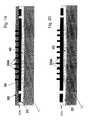
- FIG. 3 is a top-down view of the fixed part (bottom, carrier side) of the device shown in FIG. 1, according to the present invention
- FIGS. 22 through 39 show the process sequence used for fabricating the bottom carrier side of the MEM varactor device, according to the invention.
Landscapes
- Engineering & Computer Science (AREA)
- Power Engineering (AREA)
- Microelectronics & Electronic Packaging (AREA)
- Computer Hardware Design (AREA)
- Micromachines (AREA)
Abstract
Description
Claims (13)
Priority Applications (9)
| Application Number | Priority Date | Filing Date | Title |
|---|---|---|---|
| US10/278,211 US6661069B1 (en) | 2002-10-22 | 2002-10-22 | Micro-electromechanical varactor with enhanced tuning range |
| US10/459,978 US6696343B1 (en) | 2002-10-22 | 2003-06-12 | Micro-electromechanical varactor with enhanced tuning range |
| TW092120800A TWI232500B (en) | 2002-10-22 | 2003-07-30 | Micro-electromechanical varactor with enhanced tuning range |
| KR1020057004845A KR100991965B1 (en) | 2002-10-22 | 2003-09-18 | Microelectromechanical varactors and their manufacturing method |
| EP03769489A EP1556949A2 (en) | 2002-10-22 | 2003-09-18 | Micro-electromechanical varactor with enhanced tuning range |
| PCT/EP2003/012399 WO2004038916A2 (en) | 2002-10-22 | 2003-09-18 | Micro-electromechanical varactor with enhanced tuning range |
| AU2003278176A AU2003278176A1 (en) | 2002-10-22 | 2003-09-18 | Micro-electromechanical varactor with enhanced tuning range |
| JP2004546027A JP4732754B2 (en) | 2002-10-22 | 2003-09-18 | Electromechanical micro variable capacitance diode with extended tuning range |
| CNB038245213A CN100487837C (en) | 2002-10-22 | 2003-09-18 | Micro-electromechanical varactor with enhanced tuning range |
Applications Claiming Priority (1)
| Application Number | Priority Date | Filing Date | Title |
|---|---|---|---|
| US10/278,211 US6661069B1 (en) | 2002-10-22 | 2002-10-22 | Micro-electromechanical varactor with enhanced tuning range |
Related Child Applications (1)
| Application Number | Title | Priority Date | Filing Date |
|---|---|---|---|
| US10/459,978 Division US6696343B1 (en) | 2002-10-22 | 2003-06-12 | Micro-electromechanical varactor with enhanced tuning range |
Publications (1)
| Publication Number | Publication Date |
|---|---|
| US6661069B1 true US6661069B1 (en) | 2003-12-09 |
Family
ID=29711735
Family Applications (2)
| Application Number | Title | Priority Date | Filing Date |
|---|---|---|---|
| US10/278,211 Expired - Lifetime US6661069B1 (en) | 2002-10-22 | 2002-10-22 | Micro-electromechanical varactor with enhanced tuning range |
| US10/459,978 Expired - Lifetime US6696343B1 (en) | 2002-10-22 | 2003-06-12 | Micro-electromechanical varactor with enhanced tuning range |
Family Applications After (1)
| Application Number | Title | Priority Date | Filing Date |
|---|---|---|---|
| US10/459,978 Expired - Lifetime US6696343B1 (en) | 2002-10-22 | 2003-06-12 | Micro-electromechanical varactor with enhanced tuning range |
Country Status (8)
| Country | Link |
|---|---|
| US (2) | US6661069B1 (en) |
| EP (1) | EP1556949A2 (en) |
| JP (1) | JP4732754B2 (en) |
| KR (1) | KR100991965B1 (en) |
| CN (1) | CN100487837C (en) |
| AU (1) | AU2003278176A1 (en) |
| TW (1) | TWI232500B (en) |
| WO (1) | WO2004038916A2 (en) |
Cited By (27)
| Publication number | Priority date | Publication date | Assignee | Title |
|---|---|---|---|---|
| US20040147087A1 (en) * | 2002-04-25 | 2004-07-29 | Chartered Semiconductor Manufacturing Ltd. | Adjustable 3D capacitor |
| US20050258916A1 (en) * | 2004-05-19 | 2005-11-24 | Park Chul H | Circuit and method for transmitting an output signal using a microelectromechanical systems varactor and a series inductive device |
| US20060003482A1 (en) * | 2004-06-30 | 2006-01-05 | International Business Machines Corporation | Elastomeric cmos based micro electromechanical varactor |
| US7006342B2 (en) * | 2003-06-09 | 2006-02-28 | Agilent Technologies, Inc. | Variable capacitor having a rigidity-increasing feature |
| US20070183116A1 (en) * | 2006-01-24 | 2007-08-09 | Stmicroelectronics S.R.L. | Micro-electro-mechanical variable capacitor for radio frequency applications with reduced influence of a surface roughness |
| US20070251719A1 (en) * | 2006-04-27 | 2007-11-01 | Rick Sturdivant | Selective, hermetically sealed microwave package apparatus and methods |
| US20080112038A1 (en) * | 2006-11-14 | 2008-05-15 | Glimmerglass Networks, Inc. | Charging Guard With Paschen Stacking |
| WO2009002698A1 (en) * | 2007-06-22 | 2008-12-31 | Motorola, Inc. | Micro-electro-mechanical system varactor |
| US20090200642A1 (en) * | 2008-02-08 | 2009-08-13 | International Business Machines Corporation | Highly tunable metal-on-semiconductor trench varactor |
| US7664345B2 (en) | 2004-09-27 | 2010-02-16 | Qualcomm Mems Technologies, Inc. | MEMS device fabricated on a pre-patterned substrate |
| US20100259864A1 (en) * | 2009-04-13 | 2010-10-14 | Sony Corporation | Varactor element and electronic device |
| US20110102105A1 (en) * | 2009-11-02 | 2011-05-05 | Harris Corporation | Mems-based tunable filter |
| US20110188168A1 (en) * | 2010-02-03 | 2011-08-04 | Harris Corporation | High accuracy mems-based varactors |
| US20110198202A1 (en) * | 2010-02-18 | 2011-08-18 | Harris Corporation | Mems-based ultra-low power devices |
| US8308962B2 (en) | 2007-09-14 | 2012-11-13 | Qualcomm Mems Technologies, Inc. | Etching processes used in MEMS production |
| US20130175643A1 (en) * | 2011-07-12 | 2013-07-11 | Freescale Semiconductor, Inc. | Method for production of a structure with a buried electrode by direct transfer and stucture obtained in this manner |
| US8536059B2 (en) | 2007-02-20 | 2013-09-17 | Qualcomm Mems Technologies, Inc. | Equipment and methods for etching of MEMS |
| US8644896B1 (en) | 2010-12-03 | 2014-02-04 | Physical Optics Corporation | Tunable notch filter including ring resonators having a MEMS capacitor and an attenuator |
| US8830557B2 (en) | 2007-05-11 | 2014-09-09 | Qualcomm Mems Technologies, Inc. | Methods of fabricating MEMS with spacers between plates and devices formed by same |
| US8940570B2 (en) | 2012-01-03 | 2015-01-27 | International Business Machines Corporation | Micro-electro-mechanical system (MEMS) structures and design structures |
| US9093975B2 (en) | 2013-08-19 | 2015-07-28 | Harris Corporation | Microelectromechanical systems comprising differential inductors and methods for making the same |
| US9123493B2 (en) | 2014-01-23 | 2015-09-01 | Harris Corporation | Microelectromechanical switches for steering of RF signals |
| US9136822B2 (en) | 2013-08-19 | 2015-09-15 | Harris Corporation | Microelectromechanical system with a micro-scale spring suspension system and methods for making the same |
| US9172352B2 (en) | 2013-08-19 | 2015-10-27 | Harris Corporation | Integrated microelectromechanical system devices and methods for making the same |
| US9550665B2 (en) | 2014-09-17 | 2017-01-24 | Texas Instruments Incorporated | Multi-phased MEMS plate lowering and lifting system and method |
| US20170233244A1 (en) * | 2014-10-30 | 2017-08-17 | Wuxi Wio Technology Co., Ltd. | MEMS Automatic Alignment High-And-Low Comb Tooth and Manufacturing Method Thereof |
| US11335678B2 (en) * | 2019-03-04 | 2022-05-17 | Stmicroelectronics (Tours) Sas | Integrated circuit comprising a three-dimensional capacitor |
Families Citing this family (15)
| Publication number | Priority date | Publication date | Assignee | Title |
|---|---|---|---|---|
| KR100549003B1 (en) * | 2004-02-04 | 2006-02-02 | 삼성전자주식회사 | MEMS tunable capacitors with wide tuning range and method of manufacturing them |
| US7541209B2 (en) * | 2005-10-14 | 2009-06-02 | Hewlett-Packard Development Company, L.P. | Method of forming a device package having edge interconnect pad |
| JP4438786B2 (en) * | 2005-11-17 | 2010-03-24 | セイコーエプソン株式会社 | MEMS vibrator and manufacturing method thereof |
| US7560798B2 (en) * | 2006-02-27 | 2009-07-14 | International Business Machines Corporation | High performance tapered varactor |
| US7473618B1 (en) | 2008-04-22 | 2009-01-06 | International Business Machines Corporation | Temporary structure to reduce stress and warpage in a flip chip organic package |
| JP5133814B2 (en) | 2008-08-13 | 2013-01-30 | ラピスセミコンダクタ株式会社 | Variable capacitance element |
| JP2010199214A (en) * | 2009-02-24 | 2010-09-09 | Oki Semiconductor Co Ltd | Mems tunable capacitor |
| WO2010103474A1 (en) | 2009-03-11 | 2010-09-16 | Nxp B.V. | Mems electrostatic actuator |
| US20130032385A1 (en) * | 2011-08-03 | 2013-02-07 | Qualcomm Mems Technologies, Inc. | Metal thin shield on electrical device |
| JP5798094B2 (en) * | 2012-08-10 | 2015-10-21 | 日本電信電話株式会社 | Actuator |
| CN103943419A (en) * | 2014-04-15 | 2014-07-23 | 苏州锟恩电子科技有限公司 | RF MEMS switch with upper suspension beam |
| RU169456U1 (en) * | 2016-07-06 | 2017-03-21 | Общество с ограниченной ответственностью "Базовые технологии" | Three-bit RF MEMS varactor |
| CN108574017B (en) * | 2017-03-07 | 2021-08-06 | 中芯国际集成电路制造(上海)有限公司 | Varactor diode and method of forming the same |
| CN113603053B (en) * | 2018-01-23 | 2024-01-23 | 苏州明皜传感科技股份有限公司 | Micro-electromechanical system device |
| CN110148522A (en) * | 2019-05-31 | 2019-08-20 | 中国电子科技集团公司第十三研究所 | Surface Mount Type Trimming Capacitor and Capacitance Trimming Method |
Citations (2)
| Publication number | Priority date | Publication date | Assignee | Title |
|---|---|---|---|---|
| US6355534B1 (en) * | 2000-01-26 | 2002-03-12 | Intel Corporation | Variable tunable range MEMS capacitor |
| US6509620B2 (en) * | 2001-05-31 | 2003-01-21 | Hewlett-Packard Company | Flexure coupling block for motion sensor |
Family Cites Families (11)
| Publication number | Priority date | Publication date | Assignee | Title |
|---|---|---|---|---|
| JP3959763B2 (en) * | 1996-11-19 | 2007-08-15 | Tdk株式会社 | Manufacturing method of micro mechanical element |
| US6232847B1 (en) * | 1997-04-28 | 2001-05-15 | Rockwell Science Center, Llc | Trimmable singleband and tunable multiband integrated oscillator using micro-electromechanical system (MEMS) technology |
| US5982608A (en) * | 1998-01-13 | 1999-11-09 | Stmicroelectronics, Inc. | Semiconductor variable capacitor |
| EP0951069A1 (en) * | 1998-04-17 | 1999-10-20 | Interuniversitair Microelektronica Centrum Vzw | Method of fabrication of a microstructure having an inside cavity |
| US6242989B1 (en) * | 1998-09-12 | 2001-06-05 | Agere Systems Guardian Corp. | Article comprising a multi-port variable capacitor |
| SE521733C2 (en) * | 1999-06-04 | 2003-12-02 | Ericsson Telefon Ab L M | Variable capacitance, low pass filter and microelectromechanical switching arrangement |
| US6215644B1 (en) * | 1999-09-09 | 2001-04-10 | Jds Uniphase Inc. | High frequency tunable capacitors |
| US6507475B1 (en) * | 2000-06-27 | 2003-01-14 | Motorola, Inc. | Capacitive device and method of manufacture |
| FI109382B (en) * | 2000-06-27 | 2002-07-15 | Nokia Corp | The matching circuit |
| US6621137B1 (en) * | 2000-10-12 | 2003-09-16 | Intel Corporation | MEMS device integrated chip package, and method of making same |
| US6593672B2 (en) * | 2000-12-22 | 2003-07-15 | Intel Corporation | MEMS-switched stepped variable capacitor and method of making same |
-
2002
- 2002-10-22 US US10/278,211 patent/US6661069B1/en not_active Expired - Lifetime
-
2003
- 2003-06-12 US US10/459,978 patent/US6696343B1/en not_active Expired - Lifetime
- 2003-07-30 TW TW092120800A patent/TWI232500B/en not_active IP Right Cessation
- 2003-09-18 AU AU2003278176A patent/AU2003278176A1/en not_active Abandoned
- 2003-09-18 KR KR1020057004845A patent/KR100991965B1/en not_active Expired - Fee Related
- 2003-09-18 JP JP2004546027A patent/JP4732754B2/en not_active Expired - Fee Related
- 2003-09-18 CN CNB038245213A patent/CN100487837C/en not_active Expired - Fee Related
- 2003-09-18 EP EP03769489A patent/EP1556949A2/en not_active Withdrawn
- 2003-09-18 WO PCT/EP2003/012399 patent/WO2004038916A2/en not_active Ceased
Patent Citations (2)
| Publication number | Priority date | Publication date | Assignee | Title |
|---|---|---|---|---|
| US6355534B1 (en) * | 2000-01-26 | 2002-03-12 | Intel Corporation | Variable tunable range MEMS capacitor |
| US6509620B2 (en) * | 2001-05-31 | 2003-01-21 | Hewlett-Packard Company | Flexure coupling block for motion sensor |
Non-Patent Citations (1)
| Title |
|---|
| Seok et al, Transducers '01 Eurosensors XV, Jun. 10-14, 2001, "A Novel MEMS. . . (VCO)" . * |
Cited By (48)
| Publication number | Priority date | Publication date | Assignee | Title |
|---|---|---|---|---|
| US7067869B2 (en) * | 2002-04-25 | 2006-06-27 | Chartered Semiconductor Manufacturing Ltd. | Adjustable 3D capacitor |
| US20040147087A1 (en) * | 2002-04-25 | 2004-07-29 | Chartered Semiconductor Manufacturing Ltd. | Adjustable 3D capacitor |
| US7006342B2 (en) * | 2003-06-09 | 2006-02-28 | Agilent Technologies, Inc. | Variable capacitor having a rigidity-increasing feature |
| US20050258916A1 (en) * | 2004-05-19 | 2005-11-24 | Park Chul H | Circuit and method for transmitting an output signal using a microelectromechanical systems varactor and a series inductive device |
| US7126438B2 (en) * | 2004-05-19 | 2006-10-24 | Avago Technologies Wireless Ip (Singapore) Pte. Ltd. | Circuit and method for transmitting an output signal using a microelectromechanical systems varactor and a series inductive device |
| US20060003482A1 (en) * | 2004-06-30 | 2006-01-05 | International Business Machines Corporation | Elastomeric cmos based micro electromechanical varactor |
| US7265019B2 (en) | 2004-06-30 | 2007-09-04 | International Business Machines Corporation | Elastomeric CMOS based micro electromechanical varactor |
| CN100555669C (en) * | 2004-06-30 | 2009-10-28 | 国际商业机器公司 | The manufacture method of variable capacitor of micro electromechanical system |
| US7664345B2 (en) | 2004-09-27 | 2010-02-16 | Qualcomm Mems Technologies, Inc. | MEMS device fabricated on a pre-patterned substrate |
| US7489004B2 (en) * | 2006-01-24 | 2009-02-10 | Stmicroelectronics S.R.L. | Micro-electro-mechanical variable capacitor for radio frequency applications with reduced influence of a surface roughness |
| US20070183116A1 (en) * | 2006-01-24 | 2007-08-09 | Stmicroelectronics S.R.L. | Micro-electro-mechanical variable capacitor for radio frequency applications with reduced influence of a surface roughness |
| US20070251719A1 (en) * | 2006-04-27 | 2007-11-01 | Rick Sturdivant | Selective, hermetically sealed microwave package apparatus and methods |
| US7508572B2 (en) * | 2006-11-14 | 2009-03-24 | Glimmerglass Networks, Inc. | Charging guard with paschen stacking |
| US20080112038A1 (en) * | 2006-11-14 | 2008-05-15 | Glimmerglass Networks, Inc. | Charging Guard With Paschen Stacking |
| CN101606096B (en) * | 2006-11-14 | 2012-05-16 | 格雷姆格拉斯网络公司 | Charging guard with paschen stacking |
| US8536059B2 (en) | 2007-02-20 | 2013-09-17 | Qualcomm Mems Technologies, Inc. | Equipment and methods for etching of MEMS |
| US8830557B2 (en) | 2007-05-11 | 2014-09-09 | Qualcomm Mems Technologies, Inc. | Methods of fabricating MEMS with spacers between plates and devices formed by same |
| US7499257B2 (en) | 2007-06-22 | 2009-03-03 | Motorola, Inc. | Micro-electro-mechanical system varactor |
| WO2009002698A1 (en) * | 2007-06-22 | 2008-12-31 | Motorola, Inc. | Micro-electro-mechanical system varactor |
| US8308962B2 (en) | 2007-09-14 | 2012-11-13 | Qualcomm Mems Technologies, Inc. | Etching processes used in MEMS production |
| US8323516B2 (en) | 2007-09-14 | 2012-12-04 | Qualcomm Mems Technologies, Inc. | Etching processes used in MEMS production |
| US7989922B2 (en) * | 2008-02-08 | 2011-08-02 | International Business Machines Corporation | Highly tunable metal-on-semiconductor trench varactor |
| US20090200642A1 (en) * | 2008-02-08 | 2009-08-13 | International Business Machines Corporation | Highly tunable metal-on-semiconductor trench varactor |
| US8320100B2 (en) * | 2009-04-13 | 2012-11-27 | Sony Corporation | Varactor element and electronic device |
| US20100259864A1 (en) * | 2009-04-13 | 2010-10-14 | Sony Corporation | Varactor element and electronic device |
| US20110102105A1 (en) * | 2009-11-02 | 2011-05-05 | Harris Corporation | Mems-based tunable filter |
| US8436698B2 (en) | 2009-11-02 | 2013-05-07 | Harris Corporation | MEMS-based tunable filter |
| WO2011097093A3 (en) * | 2010-02-03 | 2011-11-17 | Harris Corporation | High accuracy mems-based varactors |
| US20110188168A1 (en) * | 2010-02-03 | 2011-08-04 | Harris Corporation | High accuracy mems-based varactors |
| US8373522B2 (en) | 2010-02-03 | 2013-02-12 | Harris Corporation | High accuracy MEMS-based varactors |
| US20110198202A1 (en) * | 2010-02-18 | 2011-08-18 | Harris Corporation | Mems-based ultra-low power devices |
| US8644896B1 (en) | 2010-12-03 | 2014-02-04 | Physical Optics Corporation | Tunable notch filter including ring resonators having a MEMS capacitor and an attenuator |
| US20130175643A1 (en) * | 2011-07-12 | 2013-07-11 | Freescale Semiconductor, Inc. | Method for production of a structure with a buried electrode by direct transfer and stucture obtained in this manner |
| US8692337B2 (en) * | 2011-07-12 | 2014-04-08 | Commissariat A L'energie Atomique Et Aux Energies Alternatives | Structure with a moving portion and a buried electrode for movement detection included in a multi-substrate configuration |
| US8940570B2 (en) | 2012-01-03 | 2015-01-27 | International Business Machines Corporation | Micro-electro-mechanical system (MEMS) structures and design structures |
| US9233831B2 (en) | 2012-01-03 | 2016-01-12 | International Business Machines Corporation | Micro-electro-mechanical system (MEMS) structures and design structures |
| US9580298B2 (en) | 2012-01-03 | 2017-02-28 | International Business Machines Corporation | Micro-electro-mechanical system (MEMS) structures and design structures |
| US9172352B2 (en) | 2013-08-19 | 2015-10-27 | Harris Corporation | Integrated microelectromechanical system devices and methods for making the same |
| US9093975B2 (en) | 2013-08-19 | 2015-07-28 | Harris Corporation | Microelectromechanical systems comprising differential inductors and methods for making the same |
| US9136822B2 (en) | 2013-08-19 | 2015-09-15 | Harris Corporation | Microelectromechanical system with a micro-scale spring suspension system and methods for making the same |
| US10298193B2 (en) | 2013-08-19 | 2019-05-21 | Harris Corporation | Integrated microelectromechanical system devices and methods for making the same |
| US9123493B2 (en) | 2014-01-23 | 2015-09-01 | Harris Corporation | Microelectromechanical switches for steering of RF signals |
| US9550665B2 (en) | 2014-09-17 | 2017-01-24 | Texas Instruments Incorporated | Multi-phased MEMS plate lowering and lifting system and method |
| US20170233244A1 (en) * | 2014-10-30 | 2017-08-17 | Wuxi Wio Technology Co., Ltd. | MEMS Automatic Alignment High-And-Low Comb Tooth and Manufacturing Method Thereof |
| US10077184B2 (en) * | 2014-10-30 | 2018-09-18 | Wuxi Wio Technolgy Co. | MEMS automatic alignment high-and-low comb tooth and manufacturing method thereof |
| US11335678B2 (en) * | 2019-03-04 | 2022-05-17 | Stmicroelectronics (Tours) Sas | Integrated circuit comprising a three-dimensional capacitor |
| US20220271030A1 (en) * | 2019-03-04 | 2022-08-25 | Stmicroelectronics (Tours) Sas | Integrated circuit comprising a three-dimensional capacitor |
| US11955480B2 (en) * | 2019-03-04 | 2024-04-09 | Stmicroelectronics (Tours) Sas | Integrated circuit comprising a three-dimensional capacitor |
Also Published As
| Publication number | Publication date |
|---|---|
| US6696343B1 (en) | 2004-02-24 |
| CN1689227A (en) | 2005-10-26 |
| WO2004038916A2 (en) | 2004-05-06 |
| KR20050084819A (en) | 2005-08-29 |
| KR100991965B1 (en) | 2010-11-04 |
| TWI232500B (en) | 2005-05-11 |
| AU2003278176A1 (en) | 2004-05-13 |
| JP2006518926A (en) | 2006-08-17 |
| CN100487837C (en) | 2009-05-13 |
| TW200416833A (en) | 2004-09-01 |
| JP4732754B2 (en) | 2011-07-27 |
| WO2004038916A3 (en) | 2004-08-12 |
| AU2003278176A8 (en) | 2004-05-13 |
| EP1556949A2 (en) | 2005-07-27 |
Similar Documents
| Publication | Publication Date | Title |
|---|---|---|
| US6661069B1 (en) | Micro-electromechanical varactor with enhanced tuning range | |
| US6906905B1 (en) | Micro electro-mechanical variable capacitor | |
| US6621135B1 (en) | Microrelays and microrelay fabrication and operating methods | |
| CN100575242C (en) | Fabrication method of microelectromechanical system switch and microelectromechanical device and fabrication method thereof | |
| JP3808052B2 (en) | Manufacturing method of micro electromechanical switch (MEMS) | |
| US7745892B1 (en) | Integrated MEMS switch | |
| CN1309019C (en) | Method of fabricating micro-electromechanical switches on CMOS compatible substrates | |
| JP3619430B2 (en) | Planar air bridge MEMS switch | |
| US6701779B2 (en) | Perpendicular torsion micro-electromechanical switch | |
| US7551048B2 (en) | Micro-relay and method of fabricating the same | |
| US7132723B2 (en) | Micro electro-mechanical system device with piezoelectric thin film actuator | |
| US20060003482A1 (en) | Elastomeric cmos based micro electromechanical varactor | |
| EP1945562A2 (en) | Wafer level packaging process | |
| JP2006147995A (en) | Variable capacitance element and manufacturing method thereof | |
| EP2778118B1 (en) | Integrated structure with bidirectional vertical actuation | |
| TWI573164B (en) | Electrostatically actuated micro-mechanical switching device | |
| US20080217149A1 (en) | Integrated arrangement and method for production | |
| CN116982134A (en) | Packaged MEMS switching components, apparatus and manufacturing methods | |
| JP2007535797A (en) | Beam for micromachine technology (MEMS) switches | |
| US7477884B2 (en) | Tri-state RF switch | |
| US7463125B2 (en) | Microrelays and microrelay fabrication and operating methods | |
| JP2004127871A (en) | Micro relay and method of manufacturing micro relay | |
| US6716657B1 (en) | Method for interconnecting arrays of micromechanical devices | |
| KR100493532B1 (en) | Electrostatic bi-directional microelectromechanical actuator | |
| WO2002023630A2 (en) | Micromachined silicon block vias for transferring electrical signals to the backside of a silicon wafer |
Legal Events
| Date | Code | Title | Description |
|---|---|---|---|
| AS | Assignment |
Owner name: INTERNATIONAL BUSINESS MACHINES CORPORATION, NEW Y Free format text: ASSIGNMENT OF ASSIGNORS INTEREST;ASSIGNORS:CHINTHKINDI, ANIL K.;GROVES, ROBERT A.;STEIN, KENNETH J.;AND OTHERS;REEL/FRAME:013470/0123;SIGNING DATES FROM 20021004 TO 20021017 Owner name: INTERNATIONAL BUSINESS MACHINES CORPORATION, NEW Y Free format text: ASSIGNMENT OF ASSIGNORS INTEREST;ASSIGNORS:CHINTHAKINDI, ANIL K.;GROVES, ROBERT A.;STEIN, KENNETH J.;AND OTHERS;SIGNING DATES FROM 20021004 TO 20021017;REEL/FRAME:013470/0123 |
|
| STCF | Information on status: patent grant |
Free format text: PATENTED CASE |
|
| FEPP | Fee payment procedure |
Free format text: PAYOR NUMBER ASSIGNED (ORIGINAL EVENT CODE: ASPN); ENTITY STATUS OF PATENT OWNER: LARGE ENTITY |
|
| FPAY | Fee payment |
Year of fee payment: 4 |
|
| FPAY | Fee payment |
Year of fee payment: 8 |
|
| FPAY | Fee payment |
Year of fee payment: 12 |
|
| AS | Assignment |
Owner name: GLOBALFOUNDRIES U.S. 2 LLC, NEW YORK Free format text: ASSIGNMENT OF ASSIGNORS INTEREST;ASSIGNOR:INTERNATIONAL BUSINESS MACHINES CORPORATION;REEL/FRAME:036550/0001 Effective date: 20150629 |
|
| AS | Assignment |
Owner name: GLOBALFOUNDRIES INC., CAYMAN ISLANDS Free format text: ASSIGNMENT OF ASSIGNORS INTEREST;ASSIGNORS:GLOBALFOUNDRIES U.S. 2 LLC;GLOBALFOUNDRIES U.S. INC.;REEL/FRAME:036779/0001 Effective date: 20150910 |
|
| AS | Assignment |
Owner name: WILMINGTON TRUST, NATIONAL ASSOCIATION, DELAWARE Free format text: SECURITY AGREEMENT;ASSIGNOR:GLOBALFOUNDRIES INC.;REEL/FRAME:049490/0001 Effective date: 20181127 |
|
| AS | Assignment |
Owner name: GLOBALFOUNDRIES U.S. INC., CALIFORNIA Free format text: ASSIGNMENT OF ASSIGNORS INTEREST;ASSIGNOR:GLOBALFOUNDRIES INC.;REEL/FRAME:054633/0001 Effective date: 20201022 |
|
| AS | Assignment |
Owner name: GLOBALFOUNDRIES INC., CAYMAN ISLANDS Free format text: RELEASE BY SECURED PARTY;ASSIGNOR:WILMINGTON TRUST, NATIONAL ASSOCIATION;REEL/FRAME:054636/0001 Effective date: 20201117 |
|
| AS | Assignment |
Owner name: GLOBALFOUNDRIES U.S. INC., NEW YORK Free format text: RELEASE BY SECURED PARTY;ASSIGNOR:WILMINGTON TRUST, NATIONAL ASSOCIATION;REEL/FRAME:056987/0001 Effective date: 20201117 Owner name: GLOBALFOUNDRIES U.S. INC., NEW YORK Free format text: RELEASE OF SECURITY INTEREST;ASSIGNOR:WILMINGTON TRUST, NATIONAL ASSOCIATION;REEL/FRAME:056987/0001 Effective date: 20201117 |