EP2511681B1 - Circuit intégré pour système d'imagerie spectrale - Google Patents
Circuit intégré pour système d'imagerie spectrale Download PDFInfo
- Publication number
- EP2511681B1 EP2511681B1 EP12175340.4A EP12175340A EP2511681B1 EP 2511681 B1 EP2511681 B1 EP 2511681B1 EP 12175340 A EP12175340 A EP 12175340A EP 2511681 B1 EP2511681 B1 EP 2511681B1
- Authority
- EP
- European Patent Office
- Prior art keywords
- optical
- filter
- filters
- optical filters
- different
- Prior art date
- Legal status (The legal status is an assumption and is not a legal conclusion. Google has not performed a legal analysis and makes no representation as to the accuracy of the status listed.)
- Active
Links
- 238000000701 chemical imaging Methods 0.000 title claims description 28
- 230000003595 spectral effect Effects 0.000 claims description 158
- 230000003287 optical effect Effects 0.000 claims description 157
- 238000012545 processing Methods 0.000 claims description 53
- 238000004519 manufacturing process Methods 0.000 claims description 45
- 238000003384 imaging method Methods 0.000 claims description 27
- 238000001228 spectrum Methods 0.000 claims description 19
- 238000000151 deposition Methods 0.000 claims description 14
- 230000008021 deposition Effects 0.000 claims description 14
- 238000005530 etching Methods 0.000 claims description 9
- 238000000059 patterning Methods 0.000 claims description 9
- 230000007423 decrease Effects 0.000 claims description 8
- 238000001514 detection method Methods 0.000 claims description 5
- 238000005286 illumination Methods 0.000 claims description 5
- 238000000034 method Methods 0.000 description 51
- 239000011797 cavity material Substances 0.000 description 46
- 238000013461 design Methods 0.000 description 39
- 239000010410 layer Substances 0.000 description 32
- 230000000694 effects Effects 0.000 description 31
- 239000000463 material Substances 0.000 description 28
- 230000010354 integration Effects 0.000 description 22
- 230000035945 sensitivity Effects 0.000 description 21
- 230000008569 process Effects 0.000 description 18
- 230000005540 biological transmission Effects 0.000 description 14
- 238000005516 engineering process Methods 0.000 description 14
- 239000000758 substrate Substances 0.000 description 14
- VYPSYNLAJGMNEJ-UHFFFAOYSA-N Silicium dioxide Chemical compound O=[Si]=O VYPSYNLAJGMNEJ-UHFFFAOYSA-N 0.000 description 12
- 230000003121 nonmonotonic effect Effects 0.000 description 10
- 238000003491 array Methods 0.000 description 9
- 238000002310 reflectometry Methods 0.000 description 9
- 230000006870 function Effects 0.000 description 8
- 230000009467 reduction Effects 0.000 description 8
- 238000010521 absorption reaction Methods 0.000 description 7
- 230000010363 phase shift Effects 0.000 description 7
- 238000012805 post-processing Methods 0.000 description 7
- 230000008901 benefit Effects 0.000 description 6
- 229910052681 coesite Inorganic materials 0.000 description 6
- 229910052906 cristobalite Inorganic materials 0.000 description 6
- 210000001747 pupil Anatomy 0.000 description 6
- 238000005070 sampling Methods 0.000 description 6
- 239000004065 semiconductor Substances 0.000 description 6
- 239000000377 silicon dioxide Substances 0.000 description 6
- 229910052682 stishovite Inorganic materials 0.000 description 6
- 229910052905 tridymite Inorganic materials 0.000 description 6
- 230000001419 dependent effect Effects 0.000 description 5
- 235000012239 silicon dioxide Nutrition 0.000 description 5
- 229910021417 amorphous silicon Inorganic materials 0.000 description 4
- 238000010276 construction Methods 0.000 description 4
- 230000001066 destructive effect Effects 0.000 description 4
- 239000003292 glue Substances 0.000 description 4
- 238000005457 optimization Methods 0.000 description 4
- 238000013459 approach Methods 0.000 description 3
- 238000011109 contamination Methods 0.000 description 3
- 230000003247 decreasing effect Effects 0.000 description 3
- 239000006185 dispersion Substances 0.000 description 3
- 238000003780 insertion Methods 0.000 description 3
- 230000037431 insertion Effects 0.000 description 3
- 230000002452 interceptive effect Effects 0.000 description 3
- 230000033001 locomotion Effects 0.000 description 3
- 230000004048 modification Effects 0.000 description 3
- 238000012986 modification Methods 0.000 description 3
- 238000011160 research Methods 0.000 description 3
- 239000006117 anti-reflective coating Substances 0.000 description 2
- 230000006399 behavior Effects 0.000 description 2
- 230000009286 beneficial effect Effects 0.000 description 2
- 230000008859 change Effects 0.000 description 2
- 238000004590 computer program Methods 0.000 description 2
- 238000013500 data storage Methods 0.000 description 2
- 230000007812 deficiency Effects 0.000 description 2
- 239000003989 dielectric material Substances 0.000 description 2
- 238000006073 displacement reaction Methods 0.000 description 2
- 229910052739 hydrogen Inorganic materials 0.000 description 2
- 239000001257 hydrogen Substances 0.000 description 2
- 239000002346 layers by function Substances 0.000 description 2
- 229910052751 metal Inorganic materials 0.000 description 2
- 239000002184 metal Substances 0.000 description 2
- 150000002739 metals Chemical class 0.000 description 2
- 230000003071 parasitic effect Effects 0.000 description 2
- 230000004044 response Effects 0.000 description 2
- 238000012876 topography Methods 0.000 description 2
- 230000007704 transition Effects 0.000 description 2
- UFHFLCQGNIYNRP-UHFFFAOYSA-N Hydrogen Chemical compound [H][H] UFHFLCQGNIYNRP-UHFFFAOYSA-N 0.000 description 1
- 241000183024 Populus tremula Species 0.000 description 1
- 229910000577 Silicon-germanium Inorganic materials 0.000 description 1
- 239000000654 additive Substances 0.000 description 1
- 230000000996 additive effect Effects 0.000 description 1
- 238000004458 analytical method Methods 0.000 description 1
- 230000000903 blocking effect Effects 0.000 description 1
- 239000000872 buffer Substances 0.000 description 1
- 230000015556 catabolic process Effects 0.000 description 1
- 238000012512 characterization method Methods 0.000 description 1
- 238000002425 crystallisation Methods 0.000 description 1
- 230000008025 crystallization Effects 0.000 description 1
- 230000001186 cumulative effect Effects 0.000 description 1
- 238000006731 degradation reaction Methods 0.000 description 1
- 230000006866 deterioration Effects 0.000 description 1
- 238000002059 diagnostic imaging Methods 0.000 description 1
- 238000009826 distribution Methods 0.000 description 1
- 230000008030 elimination Effects 0.000 description 1
- 238000003379 elimination reaction Methods 0.000 description 1
- 229910052737 gold Inorganic materials 0.000 description 1
- 150000002431 hydrogen Chemical class 0.000 description 1
- 230000006872 improvement Effects 0.000 description 1
- 230000010365 information processing Effects 0.000 description 1
- 230000001795 light effect Effects 0.000 description 1
- 239000004973 liquid crystal related substance Substances 0.000 description 1
- 238000001465 metallisation Methods 0.000 description 1
- 239000000203 mixture Substances 0.000 description 1
- 238000011017 operating method Methods 0.000 description 1
- 230000008520 organization Effects 0.000 description 1
- 238000005498 polishing Methods 0.000 description 1
- 238000011165 process development Methods 0.000 description 1
- 230000000644 propagated effect Effects 0.000 description 1
- 230000000630 rising effect Effects 0.000 description 1
- 238000000926 separation method Methods 0.000 description 1
- 229910052709 silver Inorganic materials 0.000 description 1
- 238000004088 simulation Methods 0.000 description 1
- 239000007787 solid Substances 0.000 description 1
- 239000010421 standard material Substances 0.000 description 1
- 238000003860 storage Methods 0.000 description 1
- 238000005728 strengthening Methods 0.000 description 1
- 239000000126 substance Substances 0.000 description 1
- 230000008685 targeting Effects 0.000 description 1
- 238000012546 transfer Methods 0.000 description 1
- 230000000007 visual effect Effects 0.000 description 1
Images


Classifications
-
- G—PHYSICS
- G01—MEASURING; TESTING
- G01J—MEASUREMENT OF INTENSITY, VELOCITY, SPECTRAL CONTENT, POLARISATION, PHASE OR PULSE CHARACTERISTICS OF INFRARED, VISIBLE OR ULTRAVIOLET LIGHT; COLORIMETRY; RADIATION PYROMETRY
- G01J3/00—Spectrometry; Spectrophotometry; Monochromators; Measuring colours
- G01J3/28—Investigating the spectrum
- G01J3/2823—Imaging spectrometer
-
- G—PHYSICS
- G01—MEASURING; TESTING
- G01J—MEASUREMENT OF INTENSITY, VELOCITY, SPECTRAL CONTENT, POLARISATION, PHASE OR PULSE CHARACTERISTICS OF INFRARED, VISIBLE OR ULTRAVIOLET LIGHT; COLORIMETRY; RADIATION PYROMETRY
- G01J3/00—Spectrometry; Spectrophotometry; Monochromators; Measuring colours
- G01J3/28—Investigating the spectrum
- G01J3/2803—Investigating the spectrum using photoelectric array detector
-
- G—PHYSICS
- G01—MEASURING; TESTING
- G01J—MEASUREMENT OF INTENSITY, VELOCITY, SPECTRAL CONTENT, POLARISATION, PHASE OR PULSE CHARACTERISTICS OF INFRARED, VISIBLE OR ULTRAVIOLET LIGHT; COLORIMETRY; RADIATION PYROMETRY
- G01J3/00—Spectrometry; Spectrophotometry; Monochromators; Measuring colours
- G01J3/12—Generating the spectrum; Monochromators
- G01J3/26—Generating the spectrum; Monochromators using multiple reflection, e.g. Fabry-Perot interferometer, variable interference filters
-
- H—ELECTRICITY
- H04—ELECTRIC COMMUNICATION TECHNIQUE
- H04N—PICTORIAL COMMUNICATION, e.g. TELEVISION
- H04N23/00—Cameras or camera modules comprising electronic image sensors; Control thereof
- H04N23/10—Cameras or camera modules comprising electronic image sensors; Control thereof for generating image signals from different wavelengths
- H04N23/11—Cameras or camera modules comprising electronic image sensors; Control thereof for generating image signals from different wavelengths for generating image signals from visible and infrared light wavelengths
-
- H—ELECTRICITY
- H04—ELECTRIC COMMUNICATION TECHNIQUE
- H04N—PICTORIAL COMMUNICATION, e.g. TELEVISION
- H04N25/00—Circuitry of solid-state image sensors [SSIS]; Control thereof
- H04N25/70—SSIS architectures; Circuits associated therewith
- H04N25/71—Charge-coupled device [CCD] sensors; Charge-transfer registers specially adapted for CCD sensors
- H04N25/75—Circuitry for providing, modifying or processing image signals from the pixel array
-
- G—PHYSICS
- G01—MEASURING; TESTING
- G01J—MEASUREMENT OF INTENSITY, VELOCITY, SPECTRAL CONTENT, POLARISATION, PHASE OR PULSE CHARACTERISTICS OF INFRARED, VISIBLE OR ULTRAVIOLET LIGHT; COLORIMETRY; RADIATION PYROMETRY
- G01J3/00—Spectrometry; Spectrophotometry; Monochromators; Measuring colours
- G01J3/12—Generating the spectrum; Monochromators
- G01J2003/1226—Interference filters
-
- G—PHYSICS
- G01—MEASURING; TESTING
- G01J—MEASUREMENT OF INTENSITY, VELOCITY, SPECTRAL CONTENT, POLARISATION, PHASE OR PULSE CHARACTERISTICS OF INFRARED, VISIBLE OR ULTRAVIOLET LIGHT; COLORIMETRY; RADIATION PYROMETRY
- G01J3/00—Spectrometry; Spectrophotometry; Monochromators; Measuring colours
- G01J3/12—Generating the spectrum; Monochromators
- G01J3/26—Generating the spectrum; Monochromators using multiple reflection, e.g. Fabry-Perot interferometer, variable interference filters
- G01J2003/265—Read out, e.g. polychromator
-
- G—PHYSICS
- G01—MEASURING; TESTING
- G01J—MEASUREMENT OF INTENSITY, VELOCITY, SPECTRAL CONTENT, POLARISATION, PHASE OR PULSE CHARACTERISTICS OF INFRARED, VISIBLE OR ULTRAVIOLET LIGHT; COLORIMETRY; RADIATION PYROMETRY
- G01J3/00—Spectrometry; Spectrophotometry; Monochromators; Measuring colours
- G01J3/28—Investigating the spectrum
- G01J3/2803—Investigating the spectrum using photoelectric array detector
- G01J2003/2806—Array and filter array
-
- G—PHYSICS
- G01—MEASURING; TESTING
- G01J—MEASUREMENT OF INTENSITY, VELOCITY, SPECTRAL CONTENT, POLARISATION, PHASE OR PULSE CHARACTERISTICS OF INFRARED, VISIBLE OR ULTRAVIOLET LIGHT; COLORIMETRY; RADIATION PYROMETRY
- G01J3/00—Spectrometry; Spectrophotometry; Monochromators; Measuring colours
- G01J3/28—Investigating the spectrum
- G01J3/2823—Imaging spectrometer
- G01J2003/2826—Multispectral imaging, e.g. filter imaging
Definitions
- the present invention relates to integrated circuits for an imaging system, the integrated circuit having an array of optical sensors, and an array of optical filters, and to corresponding systems and methods, and computer programs, and more particularly to HyperSpectral Imaging (HSI) systems, containing aspects from application driven system design and integration, and from manufacturing process technology.
- HSA HyperSpectral Imaging
- Hyperspectral imaging refers to the imaging technique of collecting and processing information from across the electromagnetic spectrum. Whereas the human eye only can see visible light, a hyperspectral imaging system can see visible light as well as from the ultraviolet to infrared. Hyperspectral sensors thus look at objects using a larger portion of the electromagnetic spectrum, as has been described at: http://en.wikipedia.org/wiki/Hyperspectral_imaging
- Certain objects leave unique 'fingerprints' across this portion of the electromagnetic spectrum. These 'fingerprints' are known as spectral signatures and enable identification of the materials that make up a scanned object.
- the hyperspectral capabilities of such imaging system enable to recognize different types of objects, all of which may appear as the same color to the human eye.
- hyperspectral imaging deals with imaging narrow spectral bands over a contiguous spectral range. It can produce the spectra for all pixels in the scene. While a sensor with 20 discrete bands covering the VIS, NIR, SWIR, MWIR, and LWIR would be considered multispectral, another sensor with also 20 bands would be considered hyperspectral when it covers the range from 500 to 700 nm with 20 10-nm wide bands. Hyperspectral sensors collect information as a set of 'images'. Each image represents a range of the electromagnetic spectrum and is also known as a spectral band.
- the third dimension can be a spectral dimension.
- spectral resolution is the width of each band of the spectrum that is captured. If the scanner picks up on a large number of fairly narrow frequency bands, it is possible to identify objects even if said objects are only captured in a handful of pixels.
- spatial resolution is a factor in addition to spectral resolution. If the pixels are too large, then multiple objects are captured in the same pixel and become difficult to identify. If the pixels are too small, then the energy captured by each sensor-cell is low, and the decreased signal-to-noise ratio reduces the reliability of measured features.
- hyperspectral cameras produce a hyperspectral datacube or image cube, consisting of a stack of 2D images in the x-y plane of the scene in which each image of the stack contains information from a different frequency or spectral band.
- the spectral range that is captured is not limited to visual light, but can also span Infra Red (IR) and/or Ultra Violet (UV).
- IR Infra Red
- UV Ultra Violet
- the 3D Image Cube is captured by a hyperspectral imager, using a sensor that is inherently a 2D sensor.
- Figure 1 shows a perspective representation of a cube with the spectral dimension extending vertically, and four views a) to d) of slices of the cube as follows: Topview (a) shows the scene that needs to be captured. Left sideview (b) shows a vertical slice from the cube, representing an image obtained by a line scanner: all spectral bands are captured for one spatial line of the scene resulting in a 1D view. Line scanners or pushbroom systems thus capture a single line of the 2D scene in all spectral bands in parallel. To cover all spatial pixels of the scene, this type of system then scans different lines over time, for example by relative movement of the scanner and the scene.
- Right sideview (c) shows a horizontal slice showing an image obtained by a starer: the complete 2D scene is captured in one spectral band. Starers or staring systems capture the complete scene in a single spectral band at a time with a 2D array of sensors and scan over different spectral bands in order to produce the 3D hyperspectral image cube.
- Bottom view (d) shows a sloping or diagonal slice through the cube, representing an image obtained by a hybrid line scanner/starer: the complete 2D scene is captured, but every spatial line is at a different height of the cube and so is a different spectral band. In this case a complete spatial image is acquired, but with every line at a different spectral band.
- Hyperspectral imaging systems or cameras can consist of different discrete components, e.g. the optical sub-system for receiving the incoming electromagnetic spectrum, the spectral unit for creating the different bands within the received spectrum and the image sensor array for detecting the different bands.
- the optical sub-system can consist of a single or a combination of different lenses, apertures and/or slits.
- the spectral unit can consist of one or more prisms, gratings, optical filters, acousto-optical tunable filters, liquid crystal tunable filters etc or a combination of these.
- a primary advantage of hyperspectral imaging is that, because an entire spectrum is acquired at each point, the operator needs no prior knowledge of the sample, and post-processing allows all available information from the dataset to be mined.
- the primary disadvantages are cost and complexity. Fast computers, sensitive detectors, and large data storage capacities are needed for analyzing hyperspectral data. Significant data storage capacity is necessary since hyperspectral cubes are large multi-dimensional datasets, potentially exceeding hundreds of megabytes. All of these factors greatly increase the cost of acquiring and processing hyperspectral data.
- An object of the invention is to provide improved apparatus or methods.
- a first aspect provides an integrated circuit for a hyperspectral imaging system according to claim 1.
- Preferred embodiments are set out in the dependent claims.
- An effect of having the thickness of the optical filter vary so as to increase at some points and decrease at other points along the line is that it enables neighbouring optical filters to be either both thicker or both thinner, to create ridges or valleys, or to enable clusters of optical filters to cover overlapping spectral bands for example.
- Another aspect provides and imaging system having such an integrated system.
- Elements or parts of the described receivers may comprise logic encoded in media for performing any kind of information processing.
- Logic may comprise software encoded in a disk or other computer-readable medium and/or instructions encoded in an application specific integrated circuit (ASIC), field programmable gate array (FPGA), or other processor or hardware.
- ASIC application specific integrated circuit
- FPGA field programmable gate array
- references to software can encompass any type of programs in any language executable directly or indirectly by a processor.
- references to logic, hardware, processor or circuitry can encompass any kind of logic or analog circuitry, integrated to any degree, and not limited to general purpose processors, digital signal processors, ASICs, FPGAs, discrete components or transistor logic gates and so on.
- References to optical are intended to encompass at least wavelengths within the human visible wavelength range and also infra red wavelengths, and shorter wavelengths, extending into the ultra violet bands, where the sensitivity to manufacturing variations in thickness of the optical filter are even more pronounced.
- the optical filters and optical sensors can be limited to a range which is any subset of these wavelengths, for example visible wavelengths only, or visible and shorter wavelengths.
- References to arrays of optical filters or arrays of optical sensors are intended to encompass 1-dimensional linear arrays, 2-dimensional arrays, rectangular or non rectangular arrays, irregularly spaced arrays, and non planar arrays for example.
- References to integrated circuits are intended to encompass at least dies or packaged dies for example having the array of optical filters monolithically integrated onto the array of sensors, or devices in which the array of optical filters is manufactured separately and added later onto the die or into the same integrated circuit package.
- references to a spectrum of wavelengths are intended to encompass a continuous spectrum or a range of nearly adjacent discrete bands for example.
- references to pixels being read out in parallel are intended to encompass instances in which all pixels have a separate line for read out, and instances where two or more pixels share a line and are output enabled at different times, giving a partially parallel arrangement.
- a combined spectral unit with image sensor array It is desirable to have a combined spectral unit with image sensor array.
- This integrated component needs to be combined with an optical sub-system to form a complete hyperspectral camera system.
- Such a hyperspectral imaging system should be compact, be capable of manufacture at low cost, and be reconfigurable.
- process technology aspects are combined with the system integration and image processing techniques to alleviate the integrated circuit manufacturing process requirements.
- a hyperspectral imaging system comprising an integrated circuit with a spectral unit monolithically integrated with the array of optical sensors forming the image sensor array.
- the spectral unit is integrated with the image sensor array using semiconductor process technology, i.e. the spectral unit is post processed on the substrate comprising the image sensor array using semiconductor process technology and process steps.
- semiconductor technology are Complementary-Metal-Oxide-Semiconductor (CMOS) processing, whereby the image sensor array is a CMOS sensor, and Charge-Coupled-Device (CCD) processing, whereby the image sensor array is a CCD sensor.
- CMOS Complementary-Metal-Oxide-Semiconductor
- CCD Charge-Coupled-Device
- the imec sensor in a lower cost technology having a large critical dimension (CD), e.g. 130nm, resulting a larger pixels and smaller spatial resolution of the image sensor array.
- a large critical dimension e.g. 130nm
- a smaller critical dimension e.g. 45nm
- the image sensor array can be a front-illuminated sensor, whereby the spectral unit is post processed on top of the substrate comprising the sensor. Optionally this substrate is thinned afterwards thereby removing the bulk of the substrate and leaving a thin slice containing the image sensor array and the spectral unit monolithically integrated therewith.
- the image sensor array can be a back-illuminated sensor, whereby first the substrate comprising the sensor is thinned from the backside onwards. On backside the thinned substrate the spectral unit is then post processed.
- the spectral unit is a sequential 1D or 2D array of Fabry-Pérot filters.
- this array can be monotonic whereby the thickness of the Fabry-Pérot filters decreases in a monotonic way from one side of the array to the other.
- this array is non-monotonic whereby the thickness of the Fabry-Pérot filters varies in a non-monotonic way from one side of the array to the other side. Methods for manufacturing such Fabry-Pérot filters are disclosed.
- any order of Fabry-Pérot filters can be manufactured, preferably only 1 st order Fabry-Pérot filters are formed on the image sensor array thereby reducing the complexity for removing and/or blocking higher order components. Hence the complexity of operating the hyperspectral system is reduced.
- the spectral unit is directly post processed on the substrate comprising the sensor, the spectral unit can be made thin and such a 1 st order Fabry- Pérot filter can be manufactured.
- a monolithically integrated hyperspectral imaging with a 1 st order Fabry- Pérot filter as spectral unit typically doesn't require a focusing lens in the optical subsystem.
- spectral oversampling is used to correct for deficiencies and process tolerances in the manufacturing technology.
- the hyperspectral imaging system is designed to have a higher spectral resolution and a higher number of bands than required by the targeted application(s).
- the thus designed imaging system has a reduced sensitivity of the Fabry-Pérot filters to processing tolerances introduced, in particular by the tight specifications of a first order Fabry-Pérot filter.
- such a design enables a configurable reduction in spectral resolution by tuning the optical system at runtime for gaining speed. The need for a collimator and slit is thereby eliminated resulting in a lower cost hyperspectral imaging system.
- range extension is used to correct for deficiencies and process tolerances in the manufacturing technology.
- the sequential 1D or 2D array of Fabry-Pérot filters is designed in a particular non-monotonous ordering, range extensions and intentional overlap/reproduction of steps.
- the thus designed imaging system has a reduced sensitivity of the Fabry-Pérot filters to processing tolerances introduced, in particular by the tight specifications of a first order Fabry-Pérot filter.
- the design of the filters e.g. the thickness which defines the cavity length of the filters, can take into account the location of the particular filter on the chip to reduce the dependency on variations in the incident angle of the incoming electromagnetic spectrum.
- the filter is post-processed on top of an image sensor array and every step is aligned with a single or multiple rows or columns of the image sensor array. Every step of the wedge filters out a different spectral band.
- the sensor and wedge filter combination can be used in hyperspectral imagers of the pushbroom, line scanner type or the hybrid line scanner/starer type.
- a hyper spectral camera system can comprise an optical filter post-processed on an image sensor array as defined in the above, the system further comprising an objective lens and/or slit and/or a collimator.
- the Integrated Spectral Module is an integrated circuit forming a subsystem of this camera, and built from different optical linefilters integrated on top of an image sensor.
- Existing wedge filters are discrete components that are assembled onto the image sensor post production.
- the filter is directly post processed on top of the imager, the amount of stray light between the filter and the image sensor can be significantly reduced.
- the spectral resolution is improved with respect to discretely integrated filters.
- semiconductor imagers such as CMOS imagers or CCD imagers are used to monolithically integrate the Fabry-Perot filter.
- the proposed hyperspectral module is monolithically integrated, meaning that the filter structures are directly post-processed on top of the image sensor. This integration has very important advantages and some consequences, compared to filter structures that are separately produced and then assembled with the imager later. Advantages of monolithic integration are cost reduction through standard CMOS production steps, reduction in stray light, allow design for first order and avoid the need for a focusing lens. When compared to a hybrid integration, in which the filter structures are separately produced and then assembled with the image sensor into the hyperspectral module, the proposed approach has some very clear advantages.
- the combination of both production sequences into one combined flow leads to an overall simplification and cost reduction in the production, when compared to a hybrid integration of the filter structures that are separately produced and then later assembled with the sensor into the module.
- This is especially the case for this filter, as the post-production of the filter structures requires only CMOS compatible fabrication steps, like deposition, patterning and etching.
- CMOS compatible fabrication steps like deposition, patterning and etching.
- expensive, error prone and labor intensive assembly steps are prevented.
- a filter with 3 layers of oxide and amorphous silicon in the Bragg stack and 127 steps in the cavity around 50 lot-turns are needed, giving an additional cost of more or less 20% with respect to standard CMOS imagers.
- the number of lot turns for the deposition of the top and bottom mirror layers can even be reduced if the different layers can be deposited, one after the other, in the same tool.
- Photons that exit the filter structure above a certain pixel can cross the gap and fall onto a neighboring pixel. This effect will be heavily reduced when the gap is reduced or completely removed by a direct postprocessing of the filter onto the pixels. There can still be some cross-talk as a result of the thickness of the filter itself however, as a photon that enters the filter above one pixel can still propagate through the filter and fall onto a neighboring pixel. This is reduced by designing thinner filters and by controlling the angle of incidence.
- the extra non-functional layer gives rise to extra reflections on its boundaries if the refractive indices are not matched (See Equation 8 below) and therefore to extra stray light on top of the cross-talk discussed above.
- stray light is reduced.
- D the distance that is traveled by the stray light (D) is well within normal pixel dimensions (e.g. 1 to 15 _m). This is not the case for more macroscopic integration distances, e.g.
- the distance of the traveled light D ranges over tens to hundreds of pixels, leading to a severe deterioration of the spatial and spectral resolution.
- the distance D can become so large, an additional focus lens is required to focus the light back onto the pixel.
- the dielectric stack and metals on top of the photodiodes reflect part of the light. Together with the gap because of the heterogeneous integration and the bottom mirror of the cavity, this forms a parasitic Fabry-Perot interfering with the actual one.
- This process can be optimized with the monolithic integration as the dielectric layers in the imager become part of the bottom Bragg stack, made in similar materials (e.g. oxide) and which is not very sensitive to the width of these layers.
- the monolithic integration combined with very precise CMOS fabrication techniques, enables the construction of filter structures with much smaller thicknesses.
- the Fabry-Perot filter structure is designed to select a certain wavelength by tuning the cavity length. Thinner filters are less sensitive to the incident angle, as the internal reflections in the filters cover less distance for non-perpendicular incidence. A thicker filter will suffer from a larger displacement D of the transmitted beams, ranging well over 10 mm. This leads to a severe reduction in spatial and spectral resolution, as the light that passes through the filters will fall onto other rows or columns of pixels. This macroscopic filter hence requires a focusing lens.
- the thin filters are much less sensitive to this and the displacement D stays in most cases below the pixel dimensions, i.e. preferably in the 1 to 10nm range, for all but the largest angles of incidence and the smallest pixels sizes.
- Traditional production techniques in combination with hybrid integration of the filter structure and the image sensor, can not reach the required accuracy to fabricate Fabry-Perot filters of the first order.
- higher order Fabry-Perot structures have to be used.
- additional dichroic or other filters have to be added to the module, in order to select the required order only. This gives rise to additional energy loss, additional costs and hence reduced overall system optimality.
- the output of the filter exhibits phase differences that, when focused by a lens, take on the form of concentric circles.
- the concentric circles are a result of the different interfering waves where you have at different locations constructive and destructive interference.
- the focusing lens is needed for macroscopic filters because of the large distances covered by reflections inside the filter and in order to focus all these reflections back onto one pixel.
- the distance between the filter structure and the image sensor is very small and as the filter is designed for the first order, there is no need for a focusing lens.
- the concentric circles that are the result of the phase difference, will still be there, but will all be focused inside the same pixel and their effect is all integrated in the output of that pixel.
- the direct post-processing of the filter structure on top of an active IC, in this case the image sensor, should be compatible with the contamination, mechanical, temperature and other limitations of that IC. This means that e.g. none of the steps used in the fabrication of the filter can use materials or processing steps that would damage the image sensor below.
- the material selection has been done such that standard materials have been used, that are fully compatible with standard processing.
- Using some materials is not possible, e.g. Au or Ag, as they tend to diffuse into the different layers and into the tools and thereby negatively affect the yield of the current and even future processing steps.
- such a layer can still be acceptable as a final step (top layer), when the deposition is done outside of the normal processing line and when the tool is only used for that purpose. This can only be done as a final step, as the wafer can not enter the normal flow after this operation.
- the maximal temperature of the processing steps should not exceed a certain maximum, e.g. 400 degrees C. This also restricts the choice of materials and crystallization that is available for the design.
- a hybrid approach where the image sensor and a separately produced filter structure are assembled into a module later, there is less freedom here.
- the restrictions have to be taken into account throughout the design. If certain design choices can be made during the design of the image sensor itself, to relax the constraints on the processing of the filter (e.g. to raise the allowed temperature for post-processing), this can be taken into account too. This then leads to an optimization problem at the module level, instead of for the image sensor and the filter structures separately.
- the restriction on the filter structures always apply, as it is processed later and on top of the image sensor.
- Every pixel of the image sensor can have its own optical filter, sensitive to one specific wavelength.
- the organization of different optical filters on the sensor depends on its usage.
- a line scanner requires the same wavelength selectivity for every pixel on the same line, in which case it is here referred to as a line filter.
- Different types of filters exist.
- the type that is used in this disclosure is the Fabry-Perot Interferometer.
- Figure 2 shows Fabry-Pérot wavelength selection, (a) Fabry-Pérot working principle, with multiple light rays being reflected, which results in constructive and destructive interference, based on the wavelength of the light, on the distance l between the semi-mirrors and the incident angle ⁇ . (b) Higher orders are also selected, which results in an order selection problem.
- the filter operation is based on the well-known Fabry-Pérot principle, in which the height of each step is tuned to the filtered spectral band. Each step forms a resonant cavity of which the resonance frequency is determined by the height of the step. On the top and bottom of the cavity, a semi-transparent mirror is placed to partially reflect the light ray. Because of the reflections, an optical path difference is introduced resulting in destructive and constructive interference (depending on the incoming wavelength), as shown in figure 2a.
- the Fabry-Perot Filter is made of a transparent layer (called cavity) with two reflecting surfaces at each side of that layer.
- the transparency and reflectivity of the surfaces have to be considered with respect to the wavelength range that the Fabry-Perot filter is targeted at.
- the transmission of the light as a function of the wavelengths shows a narrow peak around a central wavelength corresponding to the resonance in the cavity.
- light in the cavity is reflected multiple times, introducing a path length difference and a phase shift for light passing through the filter.
- the multiple light rays at the output cause interference depending on the phase shift introduced in the cavity.
- the many interfering light rays lead to a very selective optical filter for which the transmission function is given by Equation 1. with ⁇ the introduced phase shift (for an incident angle ⁇ ) equal to:
- the central wavelength of the Fabry-Perot filter is only one of important optical parameters. As constructive interference always happens when the phase shift is equal to a multiple of 2, multiple wavelengths, called higher orders, will pass the filter. As indicated in figure 3 , the wavelength separation between two transmission peaks of the filter is called the Free Spectral Range. The larger this parameter, less problems with higher orders wavelengths will occur.
- a Fabry-Perot interferometer designed for first order wavelength will provide a maximum Free Spectral Range. Indeed, for a central wavelength of 700 nm in first order, the Free Spectral Range is 350 nm to the second order at 350 nm.
- a second parameter is the quality of the filter, which is defined as the bandwidth of the filter relative to the central wavelength. The bandwidth is expressed ad the Full Width Half Maximum or FWHM of the filter, which is defined as the width of the passband at half the maximum transmission, as shown in figure 3 .
- a third parameter, also indicative of the quality of the optical filter, is the finesse F of the Fabry P'erot interferometer defined in Equation 4 as the relation between the Free Spectral Range ⁇ and the FWHM ⁇ .
- Figure 4 shows two Fabry-Perot interferometers with equal cavity length but with different reflecting surfaces.
- the angle of incidence was 0° and the cavity was filled with air with a refractive index equal to 1.
- the cavity of both filters is 450 nm resulting in a central wavelength of 900 nm and a second order wavelength at 450 nm.
- the two different implementations have respectively a low (2) and high (1) finesse resulting in low (2) and high (1) FWHM for the same Free Spectral Range.
- a fourth parameter for the Fabry-Perot filter is the spectral resolution, i.e. the minimal difference in central wavelength of two neighboring spectral bands that can be resolved. This parameter depends on both the position of the central wavelength and the bandwidth of the filter. Two neighboring spectral filtered bands are said to be distinguishable if the peak in their transmission characteristic crosses at half the maximum (the 3 dB point) or below, i.e. at or below the location where the FWHM is calculated.
- the 3 dB point the maximum
- the length of the cavity can be controlled very precisely during processing and that one is able to position next spectral band so that its 3 dB point actually crosses in that 3 dB point.
- the spectral resolution of the hyperspectral module is equal to the FWHM of the optical filters, under the assumption that the FWHM of two neighboring filters is the same.
- the central wavelength of the interferometer depends on the angle of incidence of the light.
- this dependence is a cosine relationship, which is not very sensitive at angles around 0°, i.e. light perpendicular to the surface of the optical filter. This is in contrast to gratings, for which the dependency of the wavelength selection follows a sine relationship, which is much more sensitive to variations around 0° degrees.
- a Fabry-Perot interferometer can tolerate slight variations on the angle of incidence. This feature can be used at the systems level to improve on speed, sensitivity, etc.
- a second important parameter of the mirrors is their absorption, as this will determine the efficiency of the filter. If a full range of Fabry-Perot optical filters has to be constructed over a certain wavelength range, it is beneficial that these two parameters (reflectivity and absorption) stay as constant as possible over this spectral range. In that case, the wavelength range can be covered/sampled by varying only the cavity length of the Fabry- Perot filters and the materials and mirror layers can be kept constant.
- the selected wavelength range has to match the sensitivity of the selected image sensor, which is the second component of the module
- a high-n material is amorphous silicon, with reduced absorption index because of process parameter tuning, e.g. temperature and hydrogen content. Hard oxides have better tolerances but cannot be used because of the need for higher temperatures than allowed by standard CMOS processing.
- An example of such alternative mirror system is a (distributed) Bragg stack, which is formed by combining two types of dielectrics into an alternating stack of two or more materials: one with a low refractive index and one with a high refractive index.
- a first characteristic of a Bragg stack is its bandwidth, as given by equation 6, i.e. the spectral range ⁇ ⁇ over which the reflectivity is more or less constant.
- ⁇ 0 4 ⁇ 0 ⁇ arcsin n 2 ⁇ n 1 n 2 + n 1
- the bandwidth ⁇ ⁇ depends on both the central wavelength ⁇ and the refractive indices n 1 , n 2 of the selected materials.
- a certain central wavelength e.g. 600 nm spectral range around 700 nm
- SiO2 has one of the lowest refractive indices (1:46) and a very low absorption coefficient. Both parameters are stable over a very large spectral range.
- the second material in the Bragg stack will ideally need to have refractive index equal to 6:4, in addition to an absorption coefficient as close as possible to 0.
- refractive index of SiO2 can be lowered by making it porous (mix it with air, which has a refractive index of 1). This results in a need for better manufacturable refractive index equal to 5 for the same spectral range and central wavelength.
- Equation 7 the reflectivity R of such a Bragg mirror is easily controlled by the number of pairs of dielectric layers. The more layers, the higher the reflectivity and the higher the finesse of the Fabry-Perot filter that will be built with that particular mirror.
- n 0 is the refractive index of the surrounding medium
- n s is the refractive index of the substrate
- n 1 is the refractive index of the first material
- n 2 is the refractive index of the second material
- N is the number of pairs in the Bragg stack.
- One instantiation of a distributed Bragg stack is a combination of SiO2 and engineered amorphous Silicon for a central wavelength around 700nm and a range from 540 nm to 1000 nm.
- a second instantiation is a combination of SiO2 and SiGe for a central wavelength of 1500 nm and a bandwidth of 1000 nm, in casu from 1000 nm to 2000 nm.
- a consequence of using Bragg stacks for the mirror layers is an additional phase shift during the reflection of the light. This phase shift causes the central wavelength to deviate from the one given by Equation 3, but this deviation can be easily determined using e.g. simulation tools.
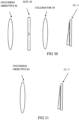
- a wedge filter as shown in figures 6a-b is an optical filter consisting of a step-like structure. These steps can be ordered to be of increasing height, in which case they form a monotonic wedge-like structure. However this ordering is not required i.e. non-monotonic structures are also possible.
- the filter is post-processed, i.e. monolithic integrated, on top of an image sensor and every step is aligned with a single of multiple rows or columns of the image sensor. Every step of the wedge filters out a different spectral band.
- the sensor and wedge filter combination can be used in hyperspectral imagers of the pushbroom, line scanner type or the hybrid line scanner/starer type.
- wedge filters are sloped structures instead of stepped structures. Due to the lower fabrication complexity, up to now sloped structures have been used. However, they are only an approximation of the desired filter, which should have a constant height for every group of sensor pixels that are intended to sense the same spectral band. This group can be arranged as a row or column or any other ordering. In the rest of this description it is assumed that the pixels that sense the same spectral band are arranged as rows or columns. Therefore the preferred structure of the wedge filter is the step structure, in which each row or column of pixels (or groups thereof) is covered with a Fabry Pérot filter of different height. The staircase structure results in different filter properties and a different selected wavelength for every (group of) row(s)/column(s), in this way resulting in a hyperspectral imager.
- the filter of the above can have every step ordered to be of increasing height in which case they form a wedge.
- the filter can have the height of each step being tuned to a filtered spectral band.
- the central wavelength of the Fabry-Perot optical filter is determined using equation 3 and can be tuned by changing: the length L of the cavity and/or the angle of incidence ⁇ of the light and/or the refractive index n of the material in the cavity
- variable cavity allows building line filters for different wavelengths by varying the cavity length L over the sensor in one direction (x or y) while keeping the 2nd dimension fixed. By varying the cavity lengths, it is possible to keep the cavity material (and its refractive index) constant. Different lines on the sensor are then sensitive to different wavelengths. Using equation 3, one can calculate the difference in height H between neighboring lines for a given spectral resolution. An implementation is given in figure 6 , which varies the length of the cavity linearly over the sensor with the same step height between the different steps (note that the height difference between the steps is exaggerated for illustrative purposes). The width W of the different steps then depends on the number of spectral bands/spectral resolution and the width of the sensor.
- FIG. 7 illustrates the variation of the selected wavelength over the complete sensor.
- the filter characteristic is shown for a line filter with a central wavelength which has very low transmission efficiency, because the reflectivity of the used mirror layers is not yet optimal in this wavelength range.
- the central wavelength gradually increases for increasing wavelengths, with a big increase in transmission efficiency at step 20 (around 600 nm), as the reflectivity of the Bragg stacks reaches the targeted performance.
- the central wavelength further increases until 1000 nm around step 120 with a second order appearing at step 95.
- the appearance of the second order is the result of the fact that a Fabry-Perot filter which is designed for wavelength ⁇ j also passes incoming wavelengths that are a multiple of ⁇ j , called higher orders. However, only those higher order wavelengths that fall in the wavelength range for which both the Fabry- Perot filter and the underlying image sensor have a reasonable efficiency should be considered.
- the affected wavelength range is approximately from 800 nm onwards.
- Figure 7 shows a drop in the transmission above 1000 nm, as only the second order is transmitted and the figure 7 shows a selected wavelength that drops back to 700 nm.
- the first and last region of this wavelength selection seem to capture only uninteresting information, as the transmission of the filter in those wavelength regions is too low or only second order information is recorded.
- these areas enable the effective spectral range to shift to the left or the right when tolerances are introduced during processing causing a global shift of the filtered wavelength range in either direction or in variations between different dies.
- Fabrication methods for manufacturing 1D or 2D Fabry-Perot filters can include binary or logarithmic construction of the staircase.
- a straightforward implementation of the staircase structure, using successive patterning and etching steps, would require a large number of processing steps in order to produce a staircase with k steps, with k typically being larger than 50.
- binary or logarithmic patterning the number of required steps can be reduced to log 2 k, as illustrated in fig 5 .
- non-monotonically rising (or sinking) wedges are used in order to absorb errors in the etching.
- the non-monotone nature can come from the fact that we etch one step of the wedge less long than necessary which results in the step being higher.
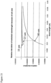
- the design will be such that the nominal design targets a wider range of wavelengths than is required by the targeted applications, which corresponds to the insertion of extra steps into the wedge filter as shown in figure 12 .
- a deviation of the produced height with respect to the nominal design will cause a shift in the effective filter range to either side of the sensor.
- the wavelength range that is requested can still be recovered by reading out different columns of pixels (after a post-production calibration step).
- the hyperspectral imaging filter set has been designed taking into account that various processing steps will always have tolerances as shown in figure 11 . These tolerances occur on all normal steps of the fabrication and controlling them is usually a cost trade-off. Every processing step can be controlled up to a certain extent and this can be improved by investing in extra process development and refinement, up to a certain extent. As a result, for many steps it is very difficult to quantify the exact limits on these variations.
- the philosophy behind the current design is to prevent the expensive and time consuming optimization steps as much as possible by taking into account these variations, if the effect of the variation can be overcome by software corrections or modifications to the design.
- the rationale behind the systems design is that the different filter lines of the hyperspectral imaging module will sample different points in the spectrum at a certain sampling interval.
- a first choice is to sample the spectrum with maximal spectral resolution. This rate can be derived from the rayleigh criterion, which states that two filters are spectrally resolvable if they cross in their 3dB point.
- a second choice is to sample the spectrum at a reduced rate, e.g. Shannon's rate to cover all frequencies in the signal. In the latter situation, small variation in the effective filter location will not have an important effect on the use of the module to sample the spectral curve. Only applications that aim to detect very narrow spectral peaks at a certain well defined wavelength will suffer from the variations. This section discusses the several causes of these variations and the techniques that we apply to cope with them.
- this planarization layer can to some extent be taken into account during the design of the filter structure. However, this layer is not a part of the active filter structure and does not have a large effect on the filter itself, as long as the correct material transition (important for the refractive index) is correctly taken into account.
- a variation in deposited thicknesses in the components of the Fabry-Perot filters, in casu the layers of the Bragg stack and the thickness of the cavity, will result in a mismatch between the designed filter and the produced filter.
- the effect of the variations on the thickness of the cavity is that: the thickness of all filters will be changed by more or less an equal amount, causing a shift of the spectral range to the right of the left of the theoretical design.
- This global shift in the selected wavelengths, either up or down, with respect to the designed filter location, can be compensated for by extending the range.
- the tolerance on the deposition of the cavity can be covered.
- the total variability on the deposited height of the cavity is maximally 20 nm, this can be related to the number of additional steps that has to be added.
- the cavity could be 10 nm higher or lower than in the design, leading to a modified range design including 2 additional steps, both for the smallest cavity length and for the biggest cavity length.
- This can be linked to the actual design by combining the needed number of spectral bands, the number of spatial lines under one band and the size of the sensor. This determines the free area on the sensor used as input to calculate the amount of extra bands and thus the maximum allowed variations on the deposition.
- Figure 12 shows a schematic representation of a hyperspectral imaging module for which the line filters are ordered from ⁇ j to ⁇ j+k , e.g. from blue to red, and for which on both sides extra line filters have been added. These filters will not be used for the nominal point, when the design is produced without significant variation in the deposition of the cavity. However, when the initial cavity deposition is off, either side of the extra line filters will fall inside the intended range and will be functional, while more filters on the other side will be disabled. This range shift can easily be calibrated post-fabrication, by illuminating the full filter structure with some known wavelengths and by storing the location of the line filter with the highest response in a memory.
- Intra-die variation can not be handled by adding more steps and therefore the intra-die variation should be limited and should be less than the difference between two steps (e.g. 3 nm). If the intra-die variation exceeds this difference, the difference between two line filters with minimal nominal wavelength difference is no longer defined. Intra-die variations are smaller than variations inter-die variations (across the wafer). Variations across the wafer cause shifting of spectrum in one direction. Extended range is foreseen to cope with this shifting.
- Fabry-Perot filters After the initial deposition of the cavity material for the Fabry-Perot filter, different filter instances, e.g. for different line filters, can be made by etching this cavity material.
- the resulting Fabry-Perot filters will be defined by their respective different cavity heights.
- the exact wavelengths response of each individual line filter will depend on the target height and the process tolerances of the various etch steps by which the final height of the step is defined.
- techniques like binary masks or logarithmic masks can be used, by which only n etch steps are required to fabricate 2n different cavity heights.
- the cumulative variation on the different etch steps that are required to define a certain target cavity length should be limited and less than the difference between two steps (e.g. 3 nm). However, some design tricks can be applied to stretch this requirement. If the optical filter is now designed that this tolerance is completely covered by introducing overlap, i.e. several parts of the mask contain the same wavelengths as shown in figure 13 , the correct wavelengths can be allocated using a calibration and software processing.
- the sharp edges that form the transition between one line filter and the next one can show rounding.
- the width of each line filter can cover multiple columns of pixels.
- the post-production characterization shows significant distortions of the filter, due to corner rounding, the affected columns can be disabled or removed in software post-processing. This is a form of redundancy and it is part of a trade-off between the cost of process optimization and the performance of the produced device, in this case a reduction in the number of used columns of pixels.
- a filter can be designed for a minimum number of spectral bands so that Shannon's sampling law is not broken. This can then be used to e.g.
- Spectral oversampling is a technique that uses the Fabry-Perot optical filter at its maximum FWHM to make it maximally spectral resolvable.
- the FWHM of these filters can be increased using system techniques. The additional spectral bands introduced by the spectral oversampling will overlap partially with the original ones, but they will make sure that all relevant information is acquired.
- Non-monotonically increasing filters provide for spectral overlap in same wedge selected to give redundant information for most critical etch steps.
- Spectral oversampling takes care of shifting wavelengths in one die: FWHM designed to be smaller than needed for spectral resolution. The number of bands is calculated using the given FWHM to cover complete spectral range. System aspects, e.g. having smaller f o , will cause FWHM to increase, hence neighboring filters will start to overlap and form one filter for 1 spectral resolution. Due to oversampling, all spectral information will be sensed and can be extracted using calibration and standard image processing.
- the hyperspectral module consisting of both the image sensor and the filter structure
- cross-component optimizations can be done.
- the proposed hyperspectral module is targeting low-cost and/or compact systems, lower quality optics can be expected.
- One effect which can be tackled in this context, is vignetting. Vignetting is a reduction of an image's brightness or saturation at the periphery compared to the image center.
- this effect is coupled to the wavelength dependent efficiency of the Fabry-Perot filter and image sensor, both effects can be co-optimized in order to flatten the wavelength dependent behavior, instead of strengthening it.
- the effect for a scanning application can be split into two components.
- the effect of the intensity fall-off perpendicular to the scanning direction can be compensated for by the illumination, as is known to those skilled in the art, by the use of so-called illumination profiles.
- Image sensors are designed for a certain wavelength range. E.g. CMOS imagers can in most cases be used in the 400 nm to 1000 nm range. However, the efficiency of the sensor is not the same over the complete range.
- Figure 15 show a schematic representation of a hyperspectral imaging module in which the line filters are no longer monotonously increasing, but for which the filters have been reordered. Filters that select wavelengths for which the sensor is the least sensitive are placed in the middle of the sensor, where no (or the least) vignetting will occur. Hence, both effects work in the opposite direction and the efficiency across the complete spectral range is flattened. This can be combined with illumination profiles, if needed, and when the application permits.
- one part of the design of the hyperspectral imaging module is the distribution or ordering of the different line filters over the image sensor.
- the design can be split into the following parts:
- the ordering of the filters does not matter, as the different filtered wavelengths can be regrouped into a hyperspectral image in software after the scanning, whatever the ordering would be.
- a method to tolerate process technology variations is applied by making use of a filter as defined in above, the wavelength range being recovered after a post-production calibration step by reading out different rows or columns of pixels covered by a filter of the same height.
- still different types of ordering make sense, when taking into account other systems aspects, like production cost, sensitivity etc.
- this ordering all line filters are ordered according to a monotonously increasing filter wavelength.
- a graphical representation of the wedge ordering is shown in figure 12 .
- One extension covers a repetition of certain line filters in the staircase structure, in order to cover the tolerances in theprocessing. If certain critical etch steps would overetch, some sampling points in the hyperspectral image would be missing. In order to prevent this, a deliberate design modification is made, that intentionally creates a non-monotonously increasing staircase structure.
- a Fabry-Perot Filter is sensitive to the angle of incidence of the light onto the filter: both the central wavelength as the FWHM depend on this incident angle.
- a special optical configuration can be used to minimize the impact of this dependency on the overall performance, e.g. when multiple filters are combined into a filter module.
- This section discusses this optical system and the trade-offs that impact the optical throughput, spectral resolution, Full Width Half Max (FWHM) of the filter, etc.
- a first system discussed below, achieves the best spectral resolution and FWHM, but at the lowest optical throughput. Opening up the stop, by replacing the slit with a variable aperture, improves the optical throughput, but worsens the FWHM and spectral resolution. This trade-off is discussed.
- the integrated wedge filter can be used in different systems setups. Depending on the system integration, the resulting performance of the wedge filter, both for speed as for spectral resolution is different.
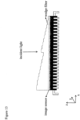
- One important aspect of the optical system, for which one example is shown in figure 18 is the size of the exit pupil.
- the size of the exit pupil has a direct effect on the size of the variation in the angle of incidence of the light onto the Fabry-Pérot filter that is formed by each step of the wedge.
- the angles between the incident ray parallel to the optical axis and the top and bottom of the exit pupil are called ⁇ and ⁇ respectively.
- the direction of the incident light can be controlled by the use of a collimator and/or a telecentric lens.
- This subsection describes the possible optical system setups to use the proposed filter module as a pure line scanning hyperspectral camera.
- the hyperspectral image cube is then constructed scanning the scene line per line.
- An objective lens for the image forming is used and a slit for selecting a single line from this image.
- the collimator is used to control (minimize) the angle of incidence of the light rays onto the optical filter or the imager. At the output of the collimator the light rays are nearly parallel. Because of the well selected location of the slit on the optical axis and the very small size of the slit, these light rays are parallel to the optical axis..
- the collimator is a plano-convex lens and is not a rotational symmetric lens. Its collimating function is restricted to the direction of the shown cross-section. In the perpendicular direction, the direction of the slit, there is no collimating effect. As a result, the image line selected by the slit is duplicated over the complete sensor with an angle of incidence perpendicular to the optical filter. Consequently, the light energy in that line is also spread over the complete sensor. Light rays that originate on image lines above or under the optical axis (e.g. by widening the slit) will also be parallel after collimation, but will not be parallel with the optical axis. The spectral resolution for a system using a collimator will therefore be independent of the f/# of the objective lens, but will be dependent on the slit size.
- the first set-up is a line-scanner consisting of an objective lens 82, slit 83, collimator 85 and integrated circuit 5 having the wedge filter on top of a standard image sensor.
- the collimator As a result of the use of the collimator, the angle of incidence of the light on top of the wedge filter is controlled well and this results in a good spectral resolution.
- the amount of light (and hence the amount of energy) that enters the system is heavily reduced. This results in larger integration times for the sensor and in an overall reduced speed.
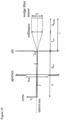
- Figure 19 details the collimated system.
- the scene, at distance O is imaged by the objective onto the slit, at distance d slit .
- the focal points of the objective are indicated by two points f.
- the Numerical Aperture NA is related to the amount of light that is passed by the objective lens.
- the light that passes through the slit falls onto the collimator, at distance f col .
- the collimated light is then projected onto the filter and sensor, at distance d wedge .
- the effect of the slit and collimation on the spectral resolution is shown in figure 20 , where the angle ⁇ is proportional to the height of the slit Y slit and represents the deviation of the selected wavelength for ⁇ and ⁇ with respect to the nominal wavelength.
- the achievable spectral resolution is in this system better than for a grating based system, as the limiting factor in grating based systems depends on the dispersion per pixel and the higher sensitivity of the grating equation (equation 10) to changes of the incident angle compared to the Fabry-Perot equation (equation 9).
- the sensitivity of the grating equation is maximal, while for the Fabry-Perot equation this sensitivity is minimal.
- the width of the spectral band for a grating based system also depends on its dispersion per mm, which depends on the pitch p. Because of this continuous dispersion, a complete spectral band is projected on a single pixel. The larger the area of the pixel, the faster the sensor, but the higher the width of the spectral band will be.
- the width of the spectral bands of the proposed wedge filter is independent of these pixel sizes and only depends on the material parameters.
- the amount of light that enters the system is heavily reduced. This is expressed through the optical throughput, which is a geometric measure of how much light is allowed to enter the optical system. Because slits have a significantly reduced area, the optical throughput of these systems is also drastically reduced, limiting the amount of light that can enter in the camera and thus limiting the speed of the camera.
- Un-collimated can be used for faster systems than grating based systems
- An alternative system setup does not have a slit and projects a complete image frame onto the sensor.
- the sensed image will therefore represent all the spatial information in the object, but as the different lines on the sensor are sensitive to different spectral bands, the different lines in the image will also contain information from different spectral bands.
- Collecting all the spectral bands for a line is done by scanning the line over the sensor and subsequently combining all spectral information corresponding to the same spatial line from different frames into one hyperspectral image cube.
- an object for which a first line is projected on the first line of the sensor sensitive to one specific spectral band b1.
- the first image line will therefore only contain information of this band b1.
- the line of the object moves to the second line on the sensor, which is sensitive to another spectral band b2.
- the second band for that line will then be collected at the same time as the first band is collected for the next line on the object. This procedure is then repeated until the complete object is scanned in all wavelength bands.
- the second system integration option uses no slit or collimator and the integrated wedge filter with sensor is combined with an objective lens into a system.
- the total system cost is reduced and the amount of light that enters the system is increased, which can lead to a faster camera.
- the angle of incidence of the light onto the different filter steps of the integrated wedge filter is less controlled, which results in a reduced spectral resolution if the lens system is not carefully designed.
- the angle of incidence depends heavily on the exit pupil of the objective and hence on the aperture.
- a large aperture (f1.65) which corresponds to a fast system, results in a spectral resolution that will be no better than 60nm from 400 to 800nm and even less between 800 and 1000nm.
- the aperture (f22) as shown in figure 22b the spectral resolution can be increased and a resolution of about 15nm can be reached across most of the range of interest.
- Careful lens design is thus needed to maximize the numerical aperture (optical throughput) and optimize the spectral resolution.
- a telecentric lens which is a lens with the chief rays in parallel with the optical axis. These lenses significantly limit the angle of incidence of the light and are perfect candidates as objective lenses for these cameras.
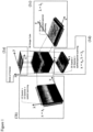
- Fig 23 integrated circuit according to an embodiment having parallel read out.
- Figure 23 shows an integrated circuit having optical sensors 40 in groups 20 underneath optical filters 10 of differing thicknesses.
- Read out circuitry 30 has output circuits A and B for each of the groups, (though output circuits are shown only for one group for the sake of clarity) so that an image having various spectral bands can be output (multi lambda image).
- some of the optical sensors are coupled to output circuit A and others to output circuit B. Of course there may be many more. In some cases, these may be one output circuit per sensor, to provide more complete parallelism in the read out. This enables the optical sensors for one group to be read out in parallel and thus read out more quickly, or a larger group to be read out in a given time.
- the group can be a line, or any other shape.
- the parallel outputs can be output in parallel, or can be multiplexed before leaving the integrated circuit.
- the optical sensors for each output circuit can be interleaved with those of other output circuits, or be in concatenated sections of a line for example.
- Figure 24 shows an integrated circuit having optical sensors 40 in groups 20 underneath optical filters 10 of differing thicknesses.
- Read out circuitry 30 is provided so that an image having various spectral bands can be output (multi lambda image).
- image having various spectral bands can be output (multi lambda image).
- the thicknesses vary so as to increase and decrease across the array, rather than varying monotonically.
- Figures 25 and 26 show examples of other profiles of thickness across the array of optical filters.
- Figure 9 shows a peak near the middle of the array.
- Figure 10 shows a saw tooth arrangement (steps too small to be resolved in this view) with clusters of optical filters having overlapping spectral bands. This gives some redundancy which can be exploited in later image processing to enable more tolerance of imprecision in the manufacture of the optical filters.
- Figs 27-29 embodiments having lambda selection.
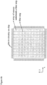
- Figure 27 shows an integrated circuit according to the invention having optical sensors 40 in groups 20 underneath optical filters 10 of differing thicknesses.
- Read out circuitry 30 has output circuits C and D for different optical filters (in a cluster of two or more of such filters), and a lambda selector 50 arranged to select either of these output circuits or interpolate between them, so that an image having various spectral bands can be output (multi lambda image). This can enable spectral sampling or spectral interpolation, which again can enable greater tolerance of errors in thickness of the optical filters. If the clusters effectively overlap with each other so that some optical filters belong to two clusters, then the wavelength selectors can be controlled to effectively shift the wavelength without necessarily subsampling.
- Figure 28 is similar to figure 27 , but with multiple output circuits for each group, which can be arranged to read out in parallel and feed parallel or multiplexed signals to the lambda selector to improve read out speeds for example.
- Figure 29 is similar to figures 27 or 28 , but with the lambda selector now implemented off chip, as a function of an image processor 53. This can enable the integrated circuit to be simpler, but may involve higher data transmission rates off the chip.
- the integrated circuit can be approximately 1 cm square for example. It can have a standard array of optical sensors (FSI) on one surface of which is formed a bottom semi transparent mirror of Al, after a planarization and/or anti reflective coating has been applied.
- the transparent layer in the wedge shape can be formed of SiO2. As discussed above, the wedge need not have a monotonic change in thickness across the array.
- a top semi transparent mirror can be formed of a layer of Al.
- the integrated circuit can have each of the optical filters having a layout as a strip across the integrated circuit, the group of sensors for a respective one of the optical filters having a layout extending as a corresponding strip.
- the group of sensors can have a layout configured as two or more lines of sensors corresponding to the layout of the strip, each of the lines of sensors being coupled to a different one of the output circuits.
- the read out circuitry has a wavelength selector for selecting between or combining (such as by interpolating between, or other combination of) read out signals of corresponding pixels of different optical filters to tune the output to correspond to a particular wavelength.
- the locations of the optical filters can be arranged so as to have optical filters for wavelengths for which the optical sensors are less sensitive located at locations where the incident illumination will have lower intensity. Typically this is near the centre and away from edges of the sensor array.
- the locations are arranged to provide a cluster of adjacent optical filters having different thicknesses to enable detection over a first spectral band, and to provide a neighbouring cluster having different thicknesses to enable detection over a second spectral band such that the first and second spectral bands overlap.
- At least some of the sensors can be arranged in groups each receiving light from a corresponding one of the optical filters, and the read out circuitry can comprise at least one output circuit coupled to the sensors of a respective one of the groups, with a wavelength selector for selecting between or interpolating between read out signals of different groups corresponding to different ones of the optical filters, to provide an output for those groups tuned to correspond to a particular optical wavelength.
- the locations can be arranged to provide a given one of the optical filters with neighbouring strips which are both thicker or both thinner, to provide a valley or ridge structure respectively.
- the thicknesses of the optical filters can be configured to compensate for differing angle of incidence of light at different positions across the array of optical filters. In the example of a longitudinal strip filter, the angle of incidence is likely to be greater near the extremities and so the thickness should be less, so that the path length is constant.
- the locations are arranged to provide a cluster of adjacent optical filters having different thicknesses and the read out circuitry having a wavelength selector for selecting between or interpolating between read out signals of corresponding pixels of different optical filters of the cluster to tune the output to correspond to a particular wavelength.
- the wavelength selector can be arranged to output signals representing proportionately fewer wavelengths than the quantity of different optical filters provided on the array of optical filters, so as to provide a proportionate spectral subsampling.
- the wavelength selector can be arranged to output signals representing a number of wavelengths similar to a quantity of different optical filters provided on the array of optical filters, so as to provide a spectral shift.
- the amount of spectral shift can be varied according to location in the array of optical filters to compensate for manufacturing variations in optical filter thickness at different locations.
- An imaging system can have the integrated circuit and an external image processing part coupled to receive the pixel values representing the image, and to output an image processed version of the received image.
- the imaging system can be arranged to generate and store an image cube of an object, by relative motion of the integrated circuit and the object being imaged, the image cube having x and y spatial dimensions, and a spectral dimension.
- the imaging system can be arranged to apply a lambda selection or interpolation image processing function, to subsample the image cube in the spectral dimension or to shift the image cube in the spectral dimension.
- the variation according to location can be suitable to compensate for any one or more of the following: manufacturing variations in optical filter thickness at different locations, distortions owing to variation in angle of incidence of an optical path through the optical filter, higher order removal and distortions from other optical components.
- the imaging system can have any one or more of an objective lens a slit and a collimator, in an optical path leading to the array of optical filters. At least some of the optical filters can have a thickness suitable to distinguish higher order interference, and the image processor can be arranged to compensate for higher order interference effects in the rest of the image representation according to an amount of higher order interference distinguished by those optical filters.
- Some embodiments have an optical filter array with a stepped-like structure post-processed on top of an image sensor array, the filter being positioned in direct contact with the image sensor array.
- the filter array in some cases has every step of the filter aligned with a single row or column of pixels of the image sensor array. In some cases each row or column of pixels is covered with a Fabry Pérot filter of different height.
- the changes in thickness are non monotonic, to create ridges or valleys, across the array.
- a thickness of each step is tuned to a filtered spectral band.
- Methods for manufacturing non monotonic changes in the thickness of the filter array can include using a binary or logarithmic patterning technique.
- Examples of a complete HSI system can include an image processor after the optical sensor array, and optical parts before it.
- a hyper spectral camera system can consist of an optical filter array post-processed on an image sensor array as defined in the above, the system further comprising an objective lens and/or slit and/or a collimator.
- An effect of the non monotonic variation of thicknesses is to reorganise the relationship between frequency and the differing sensitivities of parts of the image sensor arrays (place high or low frequency in the middle instead of on the edge of the sensor). Also it can reduce the sensitivity of the filters to processing variations and hence can increase yield. It can enable several differing wavelengths clustered about a one wavelength to be received by different ones of the sensors and then the wavelength to be selected or processed later that is best suited.
- Non monotonic variation enables grouping of some spectral bands in a cluster (range) and to position them arbitrarily on the sensor array. This allows many things, like reordering for tolerances, compensating for fall-off, and so on.
- Monotonic wedges can do some of this but will however never be able to cope with tolerances because of etching, whether they are larger or smaller than the deposition tolerances doesn't matter.
- the non monotonic variation enables the intra cluster variation to be greater than the inter cluster variation.
- an increase in width of 1 or more steps can be provided for the most important bands for the particular application.
- Another alternative is to adapt the ordering of the different steps to match areas of maximum sensitivity of the optical parts to less sensitive areas of the sensor. So the middle of the sensor array can be used for the most important bands for the application, by making filter array have the appropriate thickness in the middle for example.
- an effect of selection according to calibration input is that the calibration input can compensate for process variations either intra-die or inter-die variations across a wafer of many dies, or even inter wafer variations, if there are enough sensors and optical filters to effectively oversample the spectrum, or to have extended range so that selector selects the best suited filters that most closely match a desired set of wavelength values.
- hyperspectral imagers that are typically research instruments, with image processing delivered as a research instrument in packages that are typically only useable by experienced and trained people on high performance infrastructure, can be overcome.
- Real-time hyperspectral image processing can enable use of such hyperspectral technology in industrial machine vision and medical imaging amongst others.
- Some of the method steps discussed above for image processing may be implemented by logic in the form of hardware or, for example, in software using a processing engine such as a microprocessor or a programmable logic device (PLD's) such as a PLA (programmable logic array), PAL (programmable array logic), FPGA (field programmable gate array).
- a processing engine such as a microprocessor or a programmable logic device (PLD's) such as a PLA (programmable logic array), PAL (programmable array logic), FPGA (field programmable gate array).
- PLA programmable logic array
- PAL programmable array logic
- FPGA field programmable gate array
- An example of a circuit with an embedded processor may be constructed as a VLSI chip around an embedded microprocessor which may be synthesized onto a single chip with the other components.
- Other suitable processors may be used and these need not be embedded, e.g. a Pentium processor as supplied by Intel Corp. USA.
- a zero wait state SRAM memory may be provided on-chip as well as a cache memory for example.
- I/O (input/output) interfaces are provided for accessing external storage e.g. via data networks.
- FIFO buffers may be used to decouple the processor from data transfer through these interfaces.
- the interface can provide network connections, i.e. suitable ports and network addresses, e.g. the interfaces may be in the form of network cards.
- Software programs may be stored in an internal ROM (read only memory) and/or on any other non-volatile memory, e.g. they may be stored in an external memory. Access to an external memory may be provided by conventional hardware which can include an external bus interface if needed, with address, data and control busses.
- Features of the method and apparatus of the present invention may be implemented as software to run on a processor. In particular image processing in accordance with the present invention may be implemented by suitable programming of the processor.
- the methods and procedures described above may be written as computer programs in a suitable computer language such as C and then compiled for the specific processor in the embedded design. For example, the software may be written in C and then compiled using a known compiler and known assembler.
- the software has code, which when executed on a processing engine provides the methods and image processor for the present invention.
- the software programs may be stored on any suitable machine readable medium such as magnetic disks, diskettes, solid state memory, tape memory, optical disks such as CD-ROM or DVD-ROM, etc. Other variations can be envisaged within the claims.
Landscapes
- Physics & Mathematics (AREA)
- Spectroscopy & Molecular Physics (AREA)
- General Physics & Mathematics (AREA)
- Engineering & Computer Science (AREA)
- Multimedia (AREA)
- Signal Processing (AREA)
- Spectrometry And Color Measurement (AREA)
- Solid State Image Pick-Up Elements (AREA)
Claims (11)
- Circuit intégré (5) pour un système d'imagerie hyperspectrale, le circuit intégré comprenant :- un réseau de capteurs optiques (40), chaque capteur optique comprenant au moins un pixel ; et- un réseau de filtres optiques (10) étant chacun configurés pour transmettre une bande de longueurs d'onde sur un ou plusieurs des capteurs optiques (40), le réseau de filtres optiques (10) étant directement post-traité sur le réseau de capteurs optiques par des étapes de fabrication compatibles CMOS, comprenant le dépôt, la création de motifs et la gravure, dans lequel les filtres le long d'une rangée du réseau ont la même sélectivité de longueur d'onde pour chaque capteur optique de la rangée ; et- des circuits de lecture (30) pour lire les valeurs de pixels du réseau de capteurs pour représenter une image ;dans lequel différents des filtres optiques (10) sont configuré pour avoir une épaisseur différente, pour laisser passer différentes bandes de longueurs d'onde au moyen d'interférences, pour permettre la détection d'un spectre de longueurs d'onde et l'emplacement des différents filtres optiques (10) étant disposés de telle sorte que, le long d'une ligne de différents filtres s'étendant à travers le réseau de filtres optiques, l'épaisseur soit agencée pour varier de manière à augmenter en certains points et diminuer en d'autres points le long de la ligne ; etdans lequel les emplacements sont disposés pour fournir une grappe de filtres optiques adjacents (10) ayant différentes épaisseurs pour permettre la détection sur une première plage spectrale, et pour fournir une grappe voisine présentant des épaisseurs différentes pour permettre une détection sur une deuxième plage spectrale telle que les première et deuxième plages spectrales se superposent,dans lequel le circuit de lecture(30) comporte un sélecteur de longueur d'onde (50) pour choisir entre ou interpoler entre les signaux de lecture des pixels correspondants de différents filtres optiques (10) au seun de chaque grappe pour régler la sortie sur une longueur d'onde particulière.
- Circuit intégré selon la revendication 1, dans lequel lesdits filtres optiques (10) sont des filtres Fabry-Pérot.
- Circuit intégré selon une quelconque des revendications 1 à 2, lesemplacements étant agencées pour fournir un filtre optique donné (10) avec des bandes voisines plus épaisses ou toutes deux plus minces, pourfournir respectivement une structure de vallée ou de crête.
- Circuit intégré selon une quelconque des revendications 1 à 3, épaisseurs des filtres optiques (10) étant configurées pour compenser différents angles d'incidence de la lumière à différentes positions sur la plage de filtres optiques.
- Circuit intégré tel que décrit dans une quelconque des revendications précédentes, au moins une partie du circuit de lecture (30) étant destinée à un groupe et comprenant au moins deux circuits de sortie couplés chacun à des capteurs optiques différents (40) de ce groupe, afin que plusieurs pixels du groupe puissent être lus en parallèle sur les circuits de sortie ; etdans lequel un ou plusieurs groupes sous le même des filtres optiques (10) peut être lu à haute voix en parallèle; etdans lequel un ou plusieurs groupes sous différents filtres optiques peuvent être lus en parallèle.
- Circuit intégré selon la revendication 6, chacun des filtres optiques (10) ayant une topologie sous forme de bande s'étendant à travers le circuit intégré, le groupe de capteurs pour un respectif des filtres optiques ayant une disposition s'étendant sous la forme d'une bande correspondante.
- Circuit intégré selon la revendication 5 ou 6, le groupe de capteurs ayant une topologie configurée comme deux ou plusieurs lignes de capteurs correspondant à la topologie de la bande, chacune des lignes de capteurs étant couplée à un circuit de sortie différent.
- Circuit intégré selon les revendications 5 à 7, dans lequel les emplacements des filtres optiques sont disposés de manière à avoir des filtres optiques (10) pour les longueurs d'onde pour lesquelles les capteurs optiques (40) sont moins sensibles situés aux emplacements où l'éclairage incident aura une intensité plus élevée.
- Circuit intégré selon une quelconque des revendications précédentes, le sélecteur de longueur d'onde (50) étant agencé pour sortir les signaux représentant proportionnellement moins de longueurs d'onde que la quantité de filtres optiques différents (10) prévue sur le réseau de filtres optiques, de manière à fournir un sous-échantillonnage spectral proportionné.
- Circuit intégré selon une quelconque des revendications précédentes, le sélecteur de longueur d'onde (50) étant agencé pour sortir les signaux représentant un certain nombre de valeurs correspondant à un certain nombre de longueurs d'onde similaire à une quantité de filtres optiques différents (10) prévue sur le réseau de filtres optiques.
- Système d'imagerie comportant le circuit intégré d'une quelconque des revendications précédentes, et une partie de traitement d'image externe (53) couplé pour recevoir les valeurs de pixels représentant l'image, et pour délivrer une version traitée de l'image reçue.
Applications Claiming Priority (3)
| Application Number | Priority Date | Filing Date | Title |
|---|---|---|---|
| US26523109P | 2009-11-30 | 2009-11-30 | |
| PCT/EP2010/068575 WO2011064403A1 (fr) | 2009-11-30 | 2010-11-30 | Circuit intégré pour système d'imagerie spectrale |
| EP10798279A EP2507599A1 (fr) | 2009-11-30 | 2010-11-30 | Circuit intégré pour système d'imagerie spectrale |
Related Parent Applications (4)
| Application Number | Title | Priority Date | Filing Date |
|---|---|---|---|
| WOPCT/EP2010/068575 Previously-Filed-Application | 2010-11-30 | ||
| EP10798279.5 Division | 2010-11-30 | ||
| PCT/EP2010/068575 Previously-Filed-Application WO2011064403A1 (fr) | 2009-11-30 | 2010-11-30 | Circuit intégré pour système d'imagerie spectrale |
| EP10798279A Division EP2507599A1 (fr) | 2009-11-30 | 2010-11-30 | Circuit intégré pour système d'imagerie spectrale |
Publications (3)
| Publication Number | Publication Date |
|---|---|
| EP2511681A2 EP2511681A2 (fr) | 2012-10-17 |
| EP2511681A3 EP2511681A3 (fr) | 2012-10-31 |
| EP2511681B1 true EP2511681B1 (fr) | 2024-05-22 |
Family
ID=43501476
Family Applications (4)
| Application Number | Title | Priority Date | Filing Date |
|---|---|---|---|
| EP12175340.4A Active EP2511681B1 (fr) | 2009-11-30 | 2010-11-30 | Circuit intégré pour système d'imagerie spectrale |
| EP10798279A Pending EP2507599A1 (fr) | 2009-11-30 | 2010-11-30 | Circuit intégré pour système d'imagerie spectrale |
| EP22200035.8A Pending EP4137790A1 (fr) | 2009-11-30 | 2010-11-30 | Circuit intégré pour système d'imagerie spectrale |
| EP12175335.4A Active EP2522968B1 (fr) | 2009-11-30 | 2010-11-30 | Circuit intégré pour système d'imagerie spectrale |
Family Applications After (3)
| Application Number | Title | Priority Date | Filing Date |
|---|---|---|---|
| EP10798279A Pending EP2507599A1 (fr) | 2009-11-30 | 2010-11-30 | Circuit intégré pour système d'imagerie spectrale |
| EP22200035.8A Pending EP4137790A1 (fr) | 2009-11-30 | 2010-11-30 | Circuit intégré pour système d'imagerie spectrale |
| EP12175335.4A Active EP2522968B1 (fr) | 2009-11-30 | 2010-11-30 | Circuit intégré pour système d'imagerie spectrale |
Country Status (7)
| Country | Link |
|---|---|
| US (6) | US9304039B2 (fr) |
| EP (4) | EP2511681B1 (fr) |
| JP (1) | JP5964235B2 (fr) |
| CN (1) | CN102741671B (fr) |
| CA (1) | CA2782235A1 (fr) |
| IL (1) | IL220038A (fr) |
| WO (1) | WO2011064403A1 (fr) |
Families Citing this family (86)
| Publication number | Priority date | Publication date | Assignee | Title |
|---|---|---|---|---|
| ES2541482T3 (es) * | 2009-12-18 | 2015-07-21 | Vito Nv (Vlaamse Instelling Voor Technologisch Onderzoek Nv) | Referenciación geométrica de datos multiespectrales |
| JP2014513292A (ja) * | 2011-04-12 | 2014-05-29 | トライパス イメージング インコーポレイテッド | 定量的ビデオ顕微鏡を準備する方法及び関連システム |
| EP2776799B1 (fr) | 2011-11-04 | 2019-05-22 | IMEC vzw | Caméra spectrale ayant des miroirs pour projection de multiples copies d'image adjacentes sur un réseau de capteurs |
| WO2013064511A1 (fr) | 2011-11-04 | 2013-05-10 | Imec | Caméra spectrale ayant des filtres intégrés et de multiples copies d'image adjacentes projetées sur un réseau de capteurs |
| JP6082401B2 (ja) | 2011-11-04 | 2017-02-15 | アイメックImec | センサアレイ上にインターリーブ配置された画像コピーのオーバーラップしたセグメントを備えたスペクトルカメラ |
| EP2773929B1 (fr) * | 2011-11-04 | 2023-12-13 | IMEC vzw | Caméra spectrale ayant une mosaïque de filtres pour chaque pixel d'image |
| WO2013116316A1 (fr) * | 2012-01-30 | 2013-08-08 | Scanadu Incorporated | Systèmes d'imagerie hyperspectrale, unités et procédés |
| US9766382B2 (en) | 2012-06-05 | 2017-09-19 | Hypermed Imaging, Inc. | Single-sensor hyperspectral imaging device |
| CA2894191C (fr) | 2012-11-07 | 2023-09-26 | Yale University | Estimation du risque d'une deficience de la lecture et du langage |
| US9405376B2 (en) * | 2012-12-10 | 2016-08-02 | Invisage Technologies, Inc. | Sensors and systems for the capture of scenes and events in space and time |
| US9304040B2 (en) * | 2013-05-21 | 2016-04-05 | The United States Of America, As Represented By The Secretary Of The Navy | Method and apparatus for multiplexed fabry-perot spectroscopy |
| EP3014875A2 (fr) * | 2013-06-24 | 2016-05-04 | Technology Innovation Momentum Fund (Israel) Limited Partnership | Système et procédé d'acquisition d'images en couleurs |
| WO2015015722A1 (fr) | 2013-07-29 | 2015-02-05 | パナソニックIpマネジメント株式会社 | Filtre optique et appareil d'imagerie par polarisation qui utilise ce dernier |
| WO2015042529A2 (fr) | 2013-09-20 | 2015-03-26 | The Regents Of The University Of California | Procédés, systèmes et dispositifs permettant d'imager des tumeurs microscopiques |
| KR102197456B1 (ko) | 2014-01-31 | 2020-12-31 | 비아비 솔루션즈 아이엔씨. | 광학 필터 및 분광계 |
| JP2015149366A (ja) * | 2014-02-05 | 2015-08-20 | キヤノン株式会社 | 半導体装置の製造方法 |
| US10097780B2 (en) | 2014-06-05 | 2018-10-09 | Invisage Technologies, Inc. | Sensors and systems for the capture of scenes and events in space and time |
| EP3172698A1 (fr) | 2014-07-24 | 2017-05-31 | Ecole Polytechnique Fédérale de Lausanne (EPFL) | Système multifonctionnel compact destiné à une spectroscopie d'imagerie |
| US9692968B2 (en) | 2014-07-31 | 2017-06-27 | Invisage Technologies, Inc. | Multi-mode power-efficient light and gesture sensing in image sensors |
| US9529246B2 (en) | 2015-01-20 | 2016-12-27 | Microsoft Technology Licensing, Llc | Transparent camera module |
| US9829614B2 (en) * | 2015-02-02 | 2017-11-28 | Synaptics Incorporated | Optical sensor using collimator |
| GB201501731D0 (en) * | 2015-02-03 | 2015-03-18 | Vito Nv | Method and system for estimating an input spectrum from sensor data |
| JP6435278B2 (ja) * | 2015-04-08 | 2018-12-05 | オリンパス株式会社 | 画像処理装置、撮像装置、画像処理方法およびプログラム |
| EP3113215A1 (fr) * | 2015-06-30 | 2017-01-04 | IMEC vzw | Procédé et dispositif pour l'inspection d'un dispositif semi-conducteur |
| CN106331442B (zh) | 2015-07-02 | 2021-01-15 | 松下知识产权经营株式会社 | 摄像装置 |
| EP3115925A1 (fr) | 2015-07-07 | 2017-01-11 | Vito NV | Procédé et système pour la transformation d'images spectrales |
| US10066990B2 (en) * | 2015-07-09 | 2018-09-04 | Verifood, Ltd. | Spatially variable filter systems and methods |
| EP3323011B1 (fr) | 2015-07-15 | 2024-03-27 | Technology Innovation Momentum Fund (Israel) Limited Partnership | Étalon de mems accordable |
| CN106361269A (zh) * | 2015-07-23 | 2017-02-01 | 松下知识产权经营株式会社 | 光检测装置以及光检测方法 |
| US10048127B2 (en) * | 2015-08-05 | 2018-08-14 | Viavi Solutions Inc. | Optical filter and spectrometer |
| CN108449958A (zh) * | 2015-09-01 | 2018-08-24 | 凯杰器械有限公司 | 高通量核酸测序系统中用于颜色探测的系统和方法 |
| TWI794145B (zh) | 2015-10-28 | 2023-03-01 | 美商加州太平洋生物科學公司 | 包含整合性帶通濾波器之光學裝置陣列 |
| EP3182079B1 (fr) * | 2015-12-14 | 2023-08-23 | ams AG | Dispositif de détection optique et procédé de fabrication d'un tel appareil |
| US9923007B2 (en) * | 2015-12-29 | 2018-03-20 | Viavi Solutions Inc. | Metal mirror based multispectral filter array |
| US9960199B2 (en) | 2015-12-29 | 2018-05-01 | Viavi Solutions Inc. | Dielectric mirror based multispectral filter array |
| KR102612412B1 (ko) | 2016-02-05 | 2023-12-12 | 한국전자통신연구원 | 이미징 센서 및 이의 제조 방법 |
| US10170509B2 (en) * | 2016-02-12 | 2019-01-01 | Viavi Solutions Inc. | Optical filter array |
| CN107192349B (zh) | 2016-03-14 | 2020-10-16 | 松下知识产权经营株式会社 | 光检测装置 |
| CN105742306B (zh) * | 2016-04-07 | 2018-12-25 | 中国科学院微电子研究所 | 一种高光谱图像传感器的单片集成方法 |
| US10596754B2 (en) * | 2016-06-03 | 2020-03-24 | The Boeing Company | Real time inspection and correction techniques for direct writing systems |
| WO2018020498A1 (fr) * | 2016-07-25 | 2018-02-01 | Ramot At Tel-Aviv University Ltd. | Système et procédé de filtrage optique |
| KR102255789B1 (ko) * | 2016-08-30 | 2021-05-26 | 삼성전자주식회사 | 광학모듈 및 이를 이용한 광학디바이스 |
| US20180084231A1 (en) * | 2016-09-21 | 2018-03-22 | Trutag Technologies, Inc. | Machine vision spectral imaging |
| US10578487B2 (en) | 2016-09-21 | 2020-03-03 | Trutag Technologies, Inc. | Calibration for fabry perot spectral measurements |
| TWI612281B (zh) | 2016-09-26 | 2018-01-21 | 財團法人工業技術研究院 | 干涉分光元件封裝裝置 |
| CN106768324A (zh) * | 2016-11-17 | 2017-05-31 | 天津津航技术物理研究所 | 一种光谱成像微型传感器 |
| EP3324161B1 (fr) * | 2016-11-18 | 2020-06-17 | Espros Photonics AG | Spectromètre et procédé de réglage d'un empilement de filtres |
| US10914961B2 (en) | 2017-02-13 | 2021-02-09 | Viavi Solutions Inc. | Optical polarizing filter |
| US10962478B2 (en) | 2017-03-24 | 2021-03-30 | Axon Dx, Llc | Spectral imaging apparatus and methods |
| US11137527B2 (en) * | 2017-05-22 | 2021-10-05 | Viavi Solutions Inc. | Mixed spacer multispectral filter |
| WO2018231982A1 (fr) * | 2017-06-13 | 2018-12-20 | X-Rite, Incorporated | Spectrophotomètre et système d'imagerie hyperspectrale |
| JP2020525055A (ja) | 2017-06-29 | 2020-08-27 | ソニー株式会社 | 医療撮影システム、方法及びコンピュータプログラム |
| FR3069923B1 (fr) | 2017-08-04 | 2019-08-30 | Tematys | Filtre de lumiere fonctionnalise pour detecteur swir ou vis-swir, et utilisations |
| EP3450938B1 (fr) * | 2017-08-30 | 2022-10-12 | IMEC vzw | Capteur d'image et appareil d'imagerie |
| US10337923B2 (en) * | 2017-09-13 | 2019-07-02 | Qualcomm Incorporated | Directional interpolation and cross-band filtering for hyperspectral imaging |
| EP3506357A1 (fr) | 2017-12-27 | 2019-07-03 | Thomson Licensing | Capteur d'images comprenant un réseau de pixels permettant de réduire l'effet d'ombrage et procédé de conception correspondant et produit-programme informatique |
| JP2019145563A (ja) * | 2018-02-16 | 2019-08-29 | ソニーセミコンダクタソリューションズ株式会社 | センサ装置および電子機器 |
| KR102540961B1 (ko) | 2018-07-05 | 2023-06-07 | 삼성전자주식회사 | 반도체 칩, 및 이를 가지는 반도체 패키지 |
| FR3084459B1 (fr) * | 2018-07-30 | 2020-07-10 | Silios Technologies | Capteur d'imagerie multispectrale pourvu de moyens de limitation de la diaphonie |
| US10739189B2 (en) * | 2018-08-09 | 2020-08-11 | Ouster, Inc. | Multispectral ranging/imaging sensor arrays and systems |
| US10732032B2 (en) | 2018-08-09 | 2020-08-04 | Ouster, Inc. | Scanning sensor array with overlapping pass bands |
| WO2020082392A1 (fr) * | 2018-10-27 | 2020-04-30 | 合刃科技(深圳)有限公司 | Capteur d'image et procédé d'imagerie |
| CN109556714A (zh) * | 2018-10-31 | 2019-04-02 | 中国科学院半导体研究所 | 太赫兹光谱芯片 |
| CN113167649B (zh) | 2019-01-16 | 2024-07-12 | 松下知识产权经营株式会社 | 光检测装置、光检测系统及滤光器阵列 |
| EP3913341A4 (fr) | 2019-01-16 | 2022-02-23 | Panasonic Intellectual Property Management Co., Ltd. | Filtre optique, dispositif de photodétection et système de photodétection |
| WO2020179282A1 (fr) | 2019-03-06 | 2020-09-10 | パナソニックIpマネジメント株式会社 | Dispositif et système de détection de lumière, et réseau de filtres |
| WO2020194146A1 (fr) * | 2019-03-26 | 2020-10-01 | 3M Innovative Properties Company | Spectromètre à réseau de capteurs |
| WO2020227980A1 (fr) * | 2019-05-15 | 2020-11-19 | 合刃科技(深圳)有限公司 | Capteur d'image, et système de capteur d'intensité lumineuse et procédé |
| JP2022533246A (ja) * | 2019-05-23 | 2022-07-21 | 東京エレクトロン株式会社 | ハイパースペクトルイメージングを使用する半導体プロセスの光学的診断 |
| US11404468B2 (en) * | 2019-06-21 | 2022-08-02 | Taiwan Semiconductor Manufacturing Company, Ltd. | Wavelength tunable narrow band filter |
| GB2587628B (en) * | 2019-10-01 | 2021-10-27 | Tracsense As | Surface condition sensor |
| US11157761B2 (en) * | 2019-10-22 | 2021-10-26 | Emza Visual Sense Ltd. | IR/Visible image camera with dual mode, active-passive-illumination, triggered by masked sensor to reduce power consumption |
| CN111029351B (zh) * | 2019-11-28 | 2023-10-27 | 天津津航技术物理研究所 | 台阶单片式光谱芯片制备方法 |
| TWI767877B (zh) | 2019-12-04 | 2022-06-11 | 新加坡商光子智能私人有限公司 | 光電處理系統 |
| TWI806042B (zh) * | 2020-04-29 | 2023-06-21 | 新加坡商光子智能私人有限公司 | 光電處理設備、系統及方法 |
| US11151736B1 (en) * | 2020-05-30 | 2021-10-19 | Center For Quantitative Cytometry | Apparatus and method to obtain unprocessed intrinsic data cubes for generating intrinsic hyper-spectral data cubes |
| US11747533B2 (en) * | 2020-07-01 | 2023-09-05 | Spectricity | Spectral sensor system using optical filter subarrays |
| KR20220010884A (ko) * | 2020-07-20 | 2022-01-27 | 에스케이하이닉스 주식회사 | 이미지 센싱 장치 |
| CN111765972A (zh) * | 2020-08-05 | 2020-10-13 | 广州星博科仪有限公司 | 基于像元镀膜技术的便携式高光谱成像仪及其拍摄方法 |
| DE102020125235A1 (de) | 2020-09-28 | 2022-03-31 | Basler Aktiengesellschaft | Kamera und Spektrophotometer |
| CN112510056A (zh) * | 2020-11-25 | 2021-03-16 | 天津津航技术物理研究所 | 像素级cmos兼容的掺氢非晶硅宽光谱图像传感器 |
| FR3132362A1 (fr) | 2022-02-01 | 2023-08-04 | Commissariat A L'energie Atomique Et Aux Energies Alternatives | Procédé de fabrication d’un filtre multispectral pour une radiation électromagnétique |
| EP4258356A1 (fr) | 2022-04-07 | 2023-10-11 | Airbus Defence and Space GmbH | Capteur a matrice de pixels et son procédé de fabrication |
| CN115200705A (zh) * | 2022-07-25 | 2022-10-18 | 长春长光辰谱科技有限公司 | 一种四探头微型光谱仪 |
| US11676306B1 (en) * | 2022-11-05 | 2023-06-13 | Center For Quantitative Cytometry | Enhancing and mapping the multi-dimentional color differentiation of intrinsic images |
| CN117824834B (zh) * | 2024-01-08 | 2024-08-27 | 优尼科(青岛)微电子有限公司 | 一种可抑制中心波长漂移的mems光谱成像系统及方法 |
Citations (2)
| Publication number | Priority date | Publication date | Assignee | Title |
|---|---|---|---|---|
| US20070148760A1 (en) * | 2005-12-22 | 2007-06-28 | Palo Alto Research Center Incorporated | Obtaining analyte information |
| WO2008017490A2 (fr) * | 2006-08-09 | 2008-02-14 | Opsolution Nanophotonics Gmbh | Filtre optique et procédé de fabrication de celui-ci, ainsi que dispositif d'étude de rayonnement électromagnétique |
Family Cites Families (31)
| Publication number | Priority date | Publication date | Assignee | Title |
|---|---|---|---|---|
| JPS6129908A (ja) | 1984-07-20 | 1986-02-12 | Matsushita Electric Ind Co Ltd | 数値制御工作機械の工具位置補正方法 |
| US4822998A (en) | 1986-05-15 | 1989-04-18 | Minolta Camera Kabushiki Kaisha | Spectral sensor with interference filter |
| US4957371A (en) | 1987-12-11 | 1990-09-18 | Santa Barbara Research Center | Wedge-filter spectrometer |
| US5144498A (en) | 1990-02-14 | 1992-09-01 | Hewlett-Packard Company | Variable wavelength light filter and sensor system |
| US5276321A (en) * | 1991-04-15 | 1994-01-04 | Geophysical & Environmental Research Corp. | Airborne multiband imaging spectrometer |
| US5159199A (en) | 1991-08-12 | 1992-10-27 | The United States Of America As Represented By The Administrator Of The National Aeronautics And Space Administration | Integrated filter and detector array for spectral imaging |
| US5379065A (en) * | 1992-06-22 | 1995-01-03 | The United States Of America As Represented By The Administrator Of The National Aeronautics And Space Administration | Programmable hyperspectral image mapper with on-array processing |
| JP2713838B2 (ja) * | 1992-10-15 | 1998-02-16 | 浜松ホトニクス株式会社 | 分光イメージングセンサ |
| DE4431412C1 (de) * | 1994-08-24 | 1996-03-14 | William Newton | Vorrichtung zur Durchführung spektroskopischer Messungen |
| JPH10271345A (ja) * | 1997-03-21 | 1998-10-09 | Toshiba Corp | 色検査装置と色検査方法と画像入力装置と画像形成装置 |
| JP4111288B2 (ja) * | 1998-07-09 | 2008-07-02 | Tdk株式会社 | 波長選択型光検出器 |
| US6038023A (en) * | 1998-07-31 | 2000-03-14 | The Research Foundation Of State University Of New York | Sensors for detection and spectroscopy |
| US6256406B1 (en) * | 1998-09-16 | 2001-07-03 | Canon Kabushiki Kaisha | Exposure compensation for digital radiography systems using selective scanning of sensor arrays |
| WO2002014811A1 (fr) * | 2000-08-17 | 2002-02-21 | Mg Microscope Gmbh | Unite de detection de lumiere et procede de detection de lumiere luminescente, et microscope confocal pour microscopie par luminescence |
| JP2004279140A (ja) * | 2003-03-13 | 2004-10-07 | Omron Corp | プラズマ分光測定装置 |
| CN1314949C (zh) * | 2003-04-09 | 2007-05-09 | 重庆大学 | 微型集成化法-珀腔阵列光谱探测器 |
| AU2003245902A1 (en) * | 2003-06-02 | 2005-01-21 | Sensovation Ag | Apparatus and methods for photo-electric measurement |
| JP4392492B2 (ja) * | 2003-06-02 | 2010-01-06 | 国立大学法人静岡大学 | 広ダイナミックレンジイメージセンサ |
| US7310153B2 (en) * | 2004-08-23 | 2007-12-18 | Palo Alto Research Center, Incorporated | Using position-sensitive detectors for wavelength determination |
| US7130041B2 (en) * | 2005-03-02 | 2006-10-31 | Li-Cor, Inc. | On-chip spectral filtering using CCD array for imaging and spectroscopy |
| CN1306288C (zh) | 2005-04-27 | 2007-03-21 | 中国科学院上海技术物理研究所 | 具有平整谐振腔层的滤光片列阵 |
| US7485877B2 (en) * | 2005-05-27 | 2009-02-03 | The Regents Of The University Of Michigan | Integrative and real-time radiation measurement methods and systems |
| US7283232B2 (en) * | 2005-06-06 | 2007-10-16 | Duke University | Optical spectroscopy with overlapping images |
| US7315667B2 (en) * | 2005-12-22 | 2008-01-01 | Palo Alto Research Center Incorporated | Propagating light to be sensed |
| JP2009544965A (ja) * | 2006-07-28 | 2009-12-17 | コーニンクレッカ フィリップス エレクトロニクス エヌ ヴィ | 一体形画像認識・スペクトル検出装置並びに画像認識及び光のスペクトル検出によって光設定値を自動的に制御する装置及び方法 |
| US20080170228A1 (en) * | 2007-01-17 | 2008-07-17 | Micron Technology, Inc. | Method and apparatus for wafer level calibration of imaging sensors |
| WO2008104928A1 (fr) * | 2007-03-01 | 2008-09-04 | Philips Intellectual Property & Standards Gmbh | Dispositif de photodétection |
| DE102007011112B4 (de) * | 2007-03-03 | 2014-10-02 | Jena-Optronik Gmbh | Verfahren zur Herstellung multispektraler Filterbaugruppen sowie eine multispektrale Filteranordnung |
| US7892713B2 (en) * | 2007-09-27 | 2011-02-22 | Eastman Kodak Company | Photoconductors containing terephthalate esters |
| GB0818822D0 (en) * | 2008-10-14 | 2008-11-19 | Edinburgh Instr | Reduction of stray light |
| CN101476936B (zh) * | 2009-01-19 | 2011-01-05 | 杭州电子科技大学 | 一种基于法-珀腔阵列式微型光谱仪 |
-
2010
- 2010-11-30 EP EP12175340.4A patent/EP2511681B1/fr active Active
- 2010-11-30 CA CA2782235A patent/CA2782235A1/fr not_active Abandoned
- 2010-11-30 JP JP2012541470A patent/JP5964235B2/ja active Active
- 2010-11-30 CN CN201080054366.7A patent/CN102741671B/zh active Active
- 2010-11-30 EP EP10798279A patent/EP2507599A1/fr active Pending
- 2010-11-30 EP EP22200035.8A patent/EP4137790A1/fr active Pending
- 2010-11-30 EP EP12175335.4A patent/EP2522968B1/fr active Active
- 2010-11-30 WO PCT/EP2010/068575 patent/WO2011064403A1/fr active Application Filing
-
2012
- 2012-05-29 IL IL220038A patent/IL220038A/en not_active IP Right Cessation
- 2012-05-29 US US13/482,860 patent/US9304039B2/en active Active
-
2016
- 2016-03-03 US US15/059,621 patent/US10139280B2/en active Active
- 2016-03-03 US US15/059,715 patent/US10260945B2/en active Active
-
2019
- 2019-03-20 US US16/359,911 patent/US10620049B2/en active Active
-
2020
- 2020-03-10 US US16/814,234 patent/US11029207B2/en active Active
-
2021
- 2021-04-27 US US17/302,217 patent/US11733095B2/en active Active
Patent Citations (2)
| Publication number | Priority date | Publication date | Assignee | Title |
|---|---|---|---|---|
| US20070148760A1 (en) * | 2005-12-22 | 2007-06-28 | Palo Alto Research Center Incorporated | Obtaining analyte information |
| WO2008017490A2 (fr) * | 2006-08-09 | 2008-02-14 | Opsolution Nanophotonics Gmbh | Filtre optique et procédé de fabrication de celui-ci, ainsi que dispositif d'étude de rayonnement électromagnétique |
Also Published As
| Publication number | Publication date |
|---|---|
| EP2522968A1 (fr) | 2012-11-14 |
| EP2511681A2 (fr) | 2012-10-17 |
| US20160252396A1 (en) | 2016-09-01 |
| EP2511681A3 (fr) | 2012-10-31 |
| WO2011064403A1 (fr) | 2011-06-03 |
| IL220038A (en) | 2017-06-29 |
| EP4137790A1 (fr) | 2023-02-22 |
| US20190285474A1 (en) | 2019-09-19 |
| JP5964235B2 (ja) | 2016-08-03 |
| CN102741671B (zh) | 2016-07-06 |
| EP2507599A1 (fr) | 2012-10-10 |
| US20160252395A1 (en) | 2016-09-01 |
| US20120327248A1 (en) | 2012-12-27 |
| JP2013512445A (ja) | 2013-04-11 |
| US20200278252A1 (en) | 2020-09-03 |
| US11733095B2 (en) | 2023-08-22 |
| US10260945B2 (en) | 2019-04-16 |
| US9304039B2 (en) | 2016-04-05 |
| IL220038A0 (en) | 2012-07-31 |
| US20210247232A1 (en) | 2021-08-12 |
| US10620049B2 (en) | 2020-04-14 |
| US11029207B2 (en) | 2021-06-08 |
| CA2782235A1 (fr) | 2011-06-03 |
| US10139280B2 (en) | 2018-11-27 |
| EP2522968B1 (fr) | 2021-04-21 |
| CN102741671A (zh) | 2012-10-17 |
Similar Documents
| Publication | Publication Date | Title |
|---|---|---|
| US11733095B2 (en) | Hyperspectral image sensor with calibration | |
| US9857222B2 (en) | Spectral camera with mosaic of filters for each image pixel | |
| US9848135B2 (en) | Spectral camera with mirrors for projecting multiple adjacent image copies onto sensor array | |
| US9772229B2 (en) | Spectral camera with integrated filters and multiple adjacent image copies projected onto sensor array | |
| US9366573B2 (en) | Spectral camera with overlapping segments of image copies interleaved onto sensor array |
Legal Events
| Date | Code | Title | Description |
|---|---|---|---|
| PUAL | Search report despatched |
Free format text: ORIGINAL CODE: 0009013 |
|
| PUAI | Public reference made under article 153(3) epc to a published international application that has entered the european phase |
Free format text: ORIGINAL CODE: 0009012 |
|
| AC | Divisional application: reference to earlier application |
Ref document number: 2507599 Country of ref document: EP Kind code of ref document: P |
|
| AK | Designated contracting states |
Kind code of ref document: A2 Designated state(s): AL AT BE BG CH CY CZ DE DK EE ES FI FR GB GR HR HU IE IS IT LI LT LU LV MC MK MT NL NO PL PT RO RS SE SI SK SM TR |
|
| AX | Request for extension of the european patent |
Extension state: BA ME |
|
| AK | Designated contracting states |
Kind code of ref document: A3 Designated state(s): AL AT BE BG CH CY CZ DE DK EE ES FI FR GB GR HR HU IE IS IT LI LT LU LV MC MK MT NL NO PL PT RO RS SE SI SK SM TR |
|
| AX | Request for extension of the european patent |
Extension state: BA ME |
|
| RIC1 | Information provided on ipc code assigned before grant |
Ipc: G01J 3/26 20060101AFI20120926BHEP Ipc: G01J 3/28 20060101ALI20120926BHEP Ipc: G01J 3/12 20060101ALN20120926BHEP |
|
| 17P | Request for examination filed |
Effective date: 20130430 |
|
| RAP1 | Party data changed (applicant data changed or rights of an application transferred) |
Owner name: IMEC VZW |
|
| STAA | Information on the status of an ep patent application or granted ep patent |
Free format text: STATUS: EXAMINATION IS IN PROGRESS |
|
| 17Q | First examination report despatched |
Effective date: 20180130 |
|
| STAA | Information on the status of an ep patent application or granted ep patent |
Free format text: STATUS: EXAMINATION IS IN PROGRESS |
|
| STAA | Information on the status of an ep patent application or granted ep patent |
Free format text: STATUS: EXAMINATION IS IN PROGRESS |
|
| GRAP | Despatch of communication of intention to grant a patent |
Free format text: ORIGINAL CODE: EPIDOSNIGR1 |
|
| STAA | Information on the status of an ep patent application or granted ep patent |
Free format text: STATUS: GRANT OF PATENT IS INTENDED |
|
| INTG | Intention to grant announced |
Effective date: 20231212 |
|
| GRAS | Grant fee paid |
Free format text: ORIGINAL CODE: EPIDOSNIGR3 |
|
| GRAA | (expected) grant |
Free format text: ORIGINAL CODE: 0009210 |
|
| STAA | Information on the status of an ep patent application or granted ep patent |
Free format text: STATUS: THE PATENT HAS BEEN GRANTED |
|
| P01 | Opt-out of the competence of the unified patent court (upc) registered |
Effective date: 20240328 |
|
| AC | Divisional application: reference to earlier application |
Ref document number: 2507599 Country of ref document: EP Kind code of ref document: P |
|
| AK | Designated contracting states |
Kind code of ref document: B1 Designated state(s): AL AT BE BG CH CY CZ DE DK EE ES FI FR GB GR HR HU IE IS IT LI LT LU LV MC MK MT NL NO PL PT RO RS SE SI SK SM TR |
|
| REG | Reference to a national code |
Ref country code: GB Ref legal event code: FG4D |
|
| REG | Reference to a national code |
Ref country code: CH Ref legal event code: EP |
|
| REG | Reference to a national code |
Ref country code: DE Ref legal event code: R096 Ref document number: 602010069391 Country of ref document: DE |
|
| REG | Reference to a national code |
Ref country code: IE Ref legal event code: FG4D |
|
| REG | Reference to a national code |
Ref country code: LT Ref legal event code: MG9D |