EP2505910A2 - Phare de véhicule automobile équipé d'une source lumineuse semi-conductrice - Google Patents
Phare de véhicule automobile équipé d'une source lumineuse semi-conductrice Download PDFInfo
- Publication number
- EP2505910A2 EP2505910A2 EP12161419A EP12161419A EP2505910A2 EP 2505910 A2 EP2505910 A2 EP 2505910A2 EP 12161419 A EP12161419 A EP 12161419A EP 12161419 A EP12161419 A EP 12161419A EP 2505910 A2 EP2505910 A2 EP 2505910A2
- Authority
- EP
- European Patent Office
- Prior art keywords
- projection lens
- light source
- semiconductor light
- motor vehicle
- optical axis
- Prior art date
- Legal status (The legal status is an assumption and is not a legal conclusion. Google has not performed a legal analysis and makes no representation as to the accuracy of the status listed.)
- Granted
Links
- 239000004065 semiconductor Substances 0.000 title claims abstract description 141
- 230000003287 optical effect Effects 0.000 claims abstract description 89
- 238000009826 distribution Methods 0.000 claims description 60
- 239000007787 solid Substances 0.000 claims description 4
- 239000000463 material Substances 0.000 claims description 3
- 230000001404 mediated effect Effects 0.000 claims description 3
- 230000007423 decrease Effects 0.000 claims description 2
- 238000003384 imaging method Methods 0.000 description 8
- 238000005286 illumination Methods 0.000 description 6
- VTYYLEPIZMXCLO-UHFFFAOYSA-L Calcium carbonate Chemical compound [Ca+2].[O-]C([O-])=O VTYYLEPIZMXCLO-UHFFFAOYSA-L 0.000 description 4
- GWEVSGVZZGPLCZ-UHFFFAOYSA-N Titan oxide Chemical compound O=[Ti]=O GWEVSGVZZGPLCZ-UHFFFAOYSA-N 0.000 description 4
- XLOMVQKBTHCTTD-UHFFFAOYSA-N Zinc monoxide Chemical compound [Zn]=O XLOMVQKBTHCTTD-UHFFFAOYSA-N 0.000 description 4
- TZCXTZWJZNENPQ-UHFFFAOYSA-L barium sulfate Chemical compound [Ba+2].[O-]S([O-])(=O)=O TZCXTZWJZNENPQ-UHFFFAOYSA-L 0.000 description 4
- 230000004907 flux Effects 0.000 description 4
- 230000000694 effects Effects 0.000 description 3
- MFEVGQHCNVXMER-UHFFFAOYSA-L 1,3,2$l^{2}-dioxaplumbetan-4-one Chemical compound [Pb+2].[O-]C([O-])=O MFEVGQHCNVXMER-UHFFFAOYSA-L 0.000 description 2
- 229910000003 Lead carbonate Inorganic materials 0.000 description 2
- 239000005083 Zinc sulfide Substances 0.000 description 2
- 230000015572 biosynthetic process Effects 0.000 description 2
- 229910000019 calcium carbonate Inorganic materials 0.000 description 2
- 239000011248 coating agent Substances 0.000 description 2
- 238000000576 coating method Methods 0.000 description 2
- 238000010276 construction Methods 0.000 description 2
- 239000000049 pigment Substances 0.000 description 2
- 229920003229 poly(methyl methacrylate) Polymers 0.000 description 2
- 239000004417 polycarbonate Substances 0.000 description 2
- 239000004926 polymethyl methacrylate Substances 0.000 description 2
- 239000004408 titanium dioxide Substances 0.000 description 2
- 239000011787 zinc oxide Substances 0.000 description 2
- 229910052984 zinc sulfide Inorganic materials 0.000 description 2
- DRDVZXDWVBGGMH-UHFFFAOYSA-N zinc;sulfide Chemical compound [S-2].[Zn+2] DRDVZXDWVBGGMH-UHFFFAOYSA-N 0.000 description 2
- 230000004075 alteration Effects 0.000 description 1
- 239000012080 ambient air Substances 0.000 description 1
- 230000008030 elimination Effects 0.000 description 1
- 238000003379 elimination reaction Methods 0.000 description 1
- 239000011521 glass Substances 0.000 description 1
- 238000000265 homogenisation Methods 0.000 description 1
- 230000003340 mental effect Effects 0.000 description 1
- 229920000515 polycarbonate Polymers 0.000 description 1
- 230000005855 radiation Effects 0.000 description 1
- 238000007493 shaping process Methods 0.000 description 1
- 239000000758 substrate Substances 0.000 description 1
Images


Classifications
-
- F—MECHANICAL ENGINEERING; LIGHTING; HEATING; WEAPONS; BLASTING
- F21—LIGHTING
- F21S—NON-PORTABLE LIGHTING DEVICES; SYSTEMS THEREOF; VEHICLE LIGHTING DEVICES SPECIALLY ADAPTED FOR VEHICLE EXTERIORS
- F21S41/00—Illuminating devices specially adapted for vehicle exteriors, e.g. headlamps
- F21S41/30—Illuminating devices specially adapted for vehicle exteriors, e.g. headlamps characterised by reflectors
- F21S41/32—Optical layout thereof
- F21S41/322—Optical layout thereof the reflector using total internal reflection
-
- F—MECHANICAL ENGINEERING; LIGHTING; HEATING; WEAPONS; BLASTING
- F21—LIGHTING
- F21S—NON-PORTABLE LIGHTING DEVICES; SYSTEMS THEREOF; VEHICLE LIGHTING DEVICES SPECIALLY ADAPTED FOR VEHICLE EXTERIORS
- F21S41/00—Illuminating devices specially adapted for vehicle exteriors, e.g. headlamps
- F21S41/10—Illuminating devices specially adapted for vehicle exteriors, e.g. headlamps characterised by the light source
- F21S41/14—Illuminating devices specially adapted for vehicle exteriors, e.g. headlamps characterised by the light source characterised by the type of light source
- F21S41/141—Light emitting diodes [LED]
- F21S41/143—Light emitting diodes [LED] the main emission direction of the LED being parallel to the optical axis of the illuminating device
-
- F—MECHANICAL ENGINEERING; LIGHTING; HEATING; WEAPONS; BLASTING
- F21—LIGHTING
- F21S—NON-PORTABLE LIGHTING DEVICES; SYSTEMS THEREOF; VEHICLE LIGHTING DEVICES SPECIALLY ADAPTED FOR VEHICLE EXTERIORS
- F21S41/00—Illuminating devices specially adapted for vehicle exteriors, e.g. headlamps
- F21S41/20—Illuminating devices specially adapted for vehicle exteriors, e.g. headlamps characterised by refractors, transparent cover plates, light guides or filters
- F21S41/25—Projection lenses
- F21S41/26—Elongated lenses
-
- F—MECHANICAL ENGINEERING; LIGHTING; HEATING; WEAPONS; BLASTING
- F21—LIGHTING
- F21S—NON-PORTABLE LIGHTING DEVICES; SYSTEMS THEREOF; VEHICLE LIGHTING DEVICES SPECIALLY ADAPTED FOR VEHICLE EXTERIORS
- F21S41/00—Illuminating devices specially adapted for vehicle exteriors, e.g. headlamps
- F21S41/20—Illuminating devices specially adapted for vehicle exteriors, e.g. headlamps characterised by refractors, transparent cover plates, light guides or filters
- F21S41/285—Refractors, transparent cover plates, light guides or filters not provided in groups F21S41/24 - F21S41/2805
-
- F—MECHANICAL ENGINEERING; LIGHTING; HEATING; WEAPONS; BLASTING
- F21—LIGHTING
- F21S—NON-PORTABLE LIGHTING DEVICES; SYSTEMS THEREOF; VEHICLE LIGHTING DEVICES SPECIALLY ADAPTED FOR VEHICLE EXTERIORS
- F21S45/00—Arrangements within vehicle lighting devices specially adapted for vehicle exteriors, for purposes other than emission or distribution of light
- F21S45/40—Cooling of lighting devices
- F21S45/47—Passive cooling, e.g. using fins, thermal conductive elements or openings
Definitions
- the present invention relates to a motor vehicle headlight according to the preamble of claim 1.
- Such a motor vehicle headlight has at least one semiconductor light source and an optical system influencing a propagation direction of the light within the headlight with a first projection lens having a main surface.
- the semiconductor light source is arranged in a focal point of the first projection lens, and the headlight is configured to generate a light distribution having a bright area and a dark area separated from the bright area by a horizontally running light-dark boundary.
- the headlight has an optical axis that connects a central point of the cut-off line with the semiconductor light source.
- a main surface is understood as an imagined surface on which the light is refracted as on the real lens. This will be explained below with reference to FIG. 1 explained in more detail.
- LED light-emitting diode
- LED light-emitting diode
- arrangements of several LEDs are referred to as a semiconductor light source.
- LEDs are usually used today with a rectangular or square light exit surface with an edge length of 0.5 mm to 2 mm, in particular with an edge length of 1 mm.
- semiconductor light sources still have comparatively low luminous fluxes and luminance, so that the low beam and high beam light distributions in the case of LED headlamps are generally formed from a plurality of light modules.
- a low-beam spot light module generates the range, ie the areas directly at the cut-off line, while the basic light module illuminates the side illumination and the area immediately in front of the vehicle (vehicle apron).
- the light distribution of the basic light module has a largely horizontal cut-off and a wide side illumination as well a soft vertical spout close to the vehicle.
- the basic light distribution corresponds largely to the light distribution of a fog lamp.
- LED basic light modules Today, different types of LED basic light modules are known.
- reflection and projection systems are used, wherein the projection systems have at least one light source with at least one primary optics, which generate an intermediate image in the focal plane of at least one projection lens.
- the intermediate image is limited by a diaphragm in the focal plane of the projection lens, in order to obtain in this way a particularly sharp cut-off.
- reflective basic light modules are known in which the light beam of the LED light source is formed by a freely shaped, usually faceted reflector surface in the desired manner.
- Semiconductor light sources are typically half space radiators. Due to the typical radiation characteristics in the half-space and favored by the sharp boundary of the semiconductor light source (by the just edged LED chips), would also offer directly imaging (ie single-image imaging without intermediate image) projection systems in which the light from the semiconductor light source is projected by an astigmatic lens directly onto the road: The semiconductor light source is located directly in the focal plane of the astigmatic lens, which space and costs for primary optics and intermediate image level can be saved.
- High illuminance levels at the cut-off line should be achieved, and at the same time the illuminance should be smooth and uniform in the direction of the vehicle apron. It should be achieved high efficiency and at the same time a long range and high illuminance.
- the light exit surface should be kept small.
- the object of the invention is to provide a motor vehicle headlight, which is characterized by an efficient, compact light module, which can produce low-beam light distributions by imaging a semiconductor light source, in particular a basic light or fog light distribution.
- the projection system according to the invention is intended to ensure high illuminance levels directly at the cut-off line and at the same time to provide far-reaching light distributions, which are at lateral and lower edges of the light distribution evenly leak to lower illuminance levels, so that a homogeneous illumination of the vehicle apron is guaranteed.
- the highest possible optical efficiency should be sought.
- Such a motor vehicle headlight has the features mentioned above and is additionally distinguished by the fact that the first projection lens is arranged so inclined with respect to the optical axis that points of the main surface of the first one lie at a radial distance from the optical axis above the optical axis Projection lens in the direction of the optical axis have an axial distance to the semiconductor light source, which differs from an axial distance, having at the same radial distance from the optical axis below the optical axis lying points of the main surface of the first projection lens.
- the inclination of the main surface is preferably 8 ° to 20 °.
- the strong inclination results in different lens zones with different magnifications.
- the lens zones closest to the light source produce large images of the light source, distant lens zones produce small images.
- the large images are preferably used for the areas of light distribution in which large dimensions and small illuminance levels are required, for example in the vehicle apron. With closely spaced lens zones, a large amount of luminous flux can be collected, thus achieving good optical efficiency. Small light source images from widely spaced lens zones are well suited for generating coverage directly at the cut-off line - with less optical Efficiency.
- a preferred embodiment is characterized in that the first projection lens has a light entry surface and is adapted to direct light incident on the light entry surface of the semiconductor light source directly into the light distribution and that points located at a radial distance from the optical axis above the optical axis Main surface of the first projection lens in the direction of the optical axis have a smaller axial distance to the semiconductor light source than at the same radial distance from the optical axis below the optical axis lying points of the main surface.
- the material thickness of the first projection lens is maximum in a central region of the lens and decreases towards the edges of the first projection lens.
- the first projection lens is realized as a concave-convex lens having a concave light entry surface and a convex light exit surface.
- a profile of the focal length of the first projection lens in a plane parallel to the horizon deviates from a profile of the focal length of the first projection lens in a vertical plane perpendicular to the horizon.
- a further preferred embodiment is characterized in that the first projection lens in a direction parallel to the horizon direction has a bi-convex cross-section and in a right angle to the horizon Vertical direction has a concave-convex cross-section.
- the distance of the semiconductor light source from the first projection lens corresponds to the focal length of the first projection lens in the vertical direction perpendicular to the horizon.
- the optics have, in addition to the first projection lens, a converging lens which is arranged between the semiconductor light source and the first projection lens.
- the additional converging lens is a Fresnel lens.
- the optics have, in addition to the first projection lens, a reflector which is arranged between the semiconductor light source and the first projection lens and adapted to emit light emanating from the semiconductor light source through reflections occurring on at least one optical surface of the reflector in such a way onto the light entrance surface of the optics to direct that this light seems to come from areas adjacent to the semiconductor light source, that the luminous area of the semiconductor light source in the vertical direction and / or in the horizontal direction is virtually widened, that is enlarged appears.
- a reflector which is arranged between the semiconductor light source and the first projection lens and adapted to emit light emanating from the semiconductor light source through reflections occurring on at least one optical surface of the reflector in such a way onto the light entrance surface of the optics to direct that this light seems to come from areas adjacent to the semiconductor light source, that the luminous area of the semiconductor light source in the vertical direction and / or in the horizontal direction is virtually widened, that is enlarged appears.
- Another embodiment is characterized in that a reflective surface of the reflector is realized as a metallic coating of a shaping structure of the reflector.
- a reflective surface of the reflector is realized as a white or diffusely reflecting surface.
- the white or diffusely reflecting surface of the reflector preferably has a layer containing titanium dioxide, zinc oxide, zinc sulfide, calcium carbonate, lead carbonate, barium sulfate or other white pigments.
- a further embodiment is characterized in that the reflector is a transparent solid, on whose reflection surface light of the semiconductor light source experiences internal total reflections.
- the reflector comprises deflecting prisms which each have optically effective surfaces in the form of a refracting light entrance surface, a refracting light exit surface and at least one reflection surface on which the light of the semiconductor light source undergoes internal total reflections.
- At least one of the optically active surfaces has a convex or concave curvature.
- the motor vehicle headlight has a diaphragm arranged directly on the semiconductor light source with a diaphragm edge which sharply delimits a light bundle emanating from the semiconductor light source.
- the semiconductor light source has a plurality of light-emitting semiconductor chips.
- a further preferred embodiment is characterized in that the plurality of semiconductor chips can be controlled independently of one another.
- the motor vehicle headlight has, in addition to the first projection lens, a second projection lens arranged in the light path behind the first projection lens and is set up to bundle light emanating from the semiconductor light source with the first projection lens into a region at a distance of one focal length from the first projection lens second projection lens located remotely between the first projection lens and the second projection lens and that the headlight is further adapted to generate the light distribution as mediated by the second projection lens image of an intermediate image formed from the focused light in the area.
- the motor vehicle headlight is set up to allow the intermediate image to be created by limiting the light bundled into the region by at least one diaphragm and / or one mirror.
- the first projection lens and / or the converging lens and / or the second projection lens and / or the reflector on an optically active surface be it a light entry surface and / or a light exit surface of a lens or a reflection surface of the reflector, light in different Directed scattering structures.
- the scattering structures impart a wavy shape to the optically effective surface. Furthermore, it is preferred that the scattering structures have a shape of vertically arranged cylinder sections.
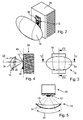
- FIG. 1a one Motor vehicle headlight 10 having at least one semiconductor light source 12 and an optical system 14 influencing a propagation of light of the semiconductor light source 12 within the headlight 10.
- the optical system 14 has a first projection lens 16 with a main surface 18.
- the semiconductor light source 12 is in one Focusing the first projection lens 16 is arranged.
- the headlamp 10 is adapted to the in FIG. 1b to produce shown light distribution 20.
- the light distribution 20 is characterized by a bright area 22 and a dark area 24, which is separated from the bright area 22 by a cut-off line 26.
- the horizontally extending line H represents the position of the horizon in a proper use of the motor vehicle headlight 10 in a motor vehicle.
- the line V corresponds to a vertical, which is arranged at a right angle to the horizontal H when used as intended.
- the bright area 22 of the light distribution 20 is just below the horizon H and has a substantially greater extent in the horizontal direction than in the vertical direction. Such a light distribution is typical for low beam and / or basic light beam distribution.
- the light distribution 20 is generated by direct imaging of the light exit surface of the semiconductor light source 12, wherein the first projection lens 16 projects an image of the semiconductor light source 12 directly into the far ahead of the motor vehicle headlight 10 apron.
- the motor vehicle headlight 10 has further semiconductor light sources and optionally further optics 14 which superimpose additional partial light light distributions on the basic light light distribution 20, for example spot light distributions, in order to generate a total light distribution adapted to the respective traffic conditions.
- An optical axis 28 of the motor vehicle extends between the semiconductor light source 12 and a central point 30 of the cut-off line 26. The central Therefore, point 30 is preferably at the crossing point of the vertical V and the horizontal H or just below it.
- the motor vehicle headlight 10 is characterized in that the first projection lens 16 is arranged inclined relative to the optical axis 28 so that points 32 of the main surface 18 of the first projection lens 16 lie in a radial distance r from the optical axis 28 above the optical axis 28
- Direction of the optical axis 28 have an axial distance d_32 to the semiconductor light source 12, which differs from a distance d_34 that a lying at the same radial distance r from the optical axis 28 below the optical axis 28 point 34 of the main surface 18 of the first projection lens sixteenth having.
- the main surface is a mental construction produced in the following manner.
- the direction of the exiting beam 56, 58 differs on the entrance and upon the exit from the first projection lens 16, refraction changes direction from the direction of the exiting beam 56, 58.
- this twofold change in direction is thought to be replaced by a single change of direction occurring within the lens at a point where the incoming beam 50, 52 and the associated exiting beam 56, 58 would intersect if no change in direction took place at the light entry surface 48 and at the light exit surface 54.
- the set of all possible intersections that are According to the main surface 18 of the first projection lens 16 relative to the optical axis 28 is arranged inclined so that the axial distances d_32 and d_34 of the same radial distance r above and below the optical axis 28 lying points 32 and 34 of the main surface 18 substantially different from each other.
- the semiconductor light source 12 consists of one or more semiconductor chips, which can be switched on and off together or separately.
- embodiments with five semiconductor chips are presented in this application.
- the number of semiconductor chips may also be less than or greater than five, and that the semiconductor chips need not only be arranged in a single row, as in embodiments discussed herein. Rather, the chips can also be mounted on the circuit carrier 36 in a matrix-like manner in rows and columns or in another, preferably regular arrangement.
- the circuit carrier 36 is preferably a rigid or flexible printed circuit board on which the semiconductor chips of the semiconductor light source 12 are attached and through which the semiconductor chips are electrically contacted.
- the circuit carrier 36 is adapted to receive the resulting during operation of the semiconductor light source 12 electrical heat loss and forward to a thermally coupled to the circuit carrier 36 heat sink 38, which emits the heat loss to the ambient air.
- the mounting of the semiconductor light source 12 in the headlight 10 is preferably relative to the first projection lens 16 so that the light exit surface of the semiconductor light source 12 is located in a Petzval surface 40 of the first projection lens 16.
- the Petzval area 40 is the area of all points that are sharply imaged by the projection lens 16. This means in particular that the semiconductor light source 12 is arranged in a focal point of the first projection lens 16.
- the structural elements described so far form a light module 42.
- This light module 42 is alone or together with other light modules of the headlamp 10 in a housing 44.
- the housing 44 has a in the FIG. 1 to the right light exit opening, which is covered by a transparent cover 46.
- FIG. 2 shows a perspective view of a heat sink 38 with mounted circuit substrate 36 and mounted thereon a semiconductor light source 12, which consists of a plurality of horizontally juxtaposed semiconductor chips, together with a first projection lens 16.
- Die FIG. 2 serves in particular to illustrate the subject matter of FIGS. 3 to 5 ,
- FIG. 3 shows a front view of the subject of FIG. 2 , ie a view of the subject of the FIG. 2 as it results from a viewing direction opposite to the light emission direction. From this line of sight, one sees the light exit surface 54 of the first projection lens 16 in front of the heat sink 38
- FIG. 3 shows in particular a preferred embodiment, which is characterized in that the first projection lens 16 in the direction of a horizontal has a greater extent than in the direction of a vertical.
- the direction of the vertical of the sectional plane IV-IV and the direction of the horizontal of the sectional plane VV corresponds in the FIG. 3 ,
- FIG. 4 shows the subject of the FIG. 3 in vertical section IV-IV
- the FIG. 5 shows the subject of the FIG. 3 in horizontal section VV.
- the vertical section shows a profile of the first projection lens 16, which is inclined about an axis parallel to the horizon H and perpendicular to the optical axis 28.
- a lens mold as shown in FIG FIG.
- the lens edge in particular the edge of the light source 12 facing lens surface (light entrance surface) 48 above the optical axis 28 is significantly closer to the light source 12 than below the optical axis 28.
- the profile of the vertical cross section through the In this case, the first projection lens 16 corresponds to the profile of a converging lens, since the material thickness of the first projection lens 16 in the region of the optical axis 28 is greatest and falls toward the edge of the lens.
- FIGS. 4 and 5 show the respective components shown there on the same scale.
- a comparison of FIGS. 4 and 5 shows therefore in particular that the lens cross sections in the horizontal section of FIG. 5 and the vertical section of the FIG. 4 have different curvatures and thus different focal lengths.
- the radii of curvature in horizontal section are much larger than the radii of curvature in vertical section.
- the first projection lens 16 generates a highly divergent light beam in the horizontal sectional plane, resulting in the FIG. 5 is represented by the wide opening angle 59.
- the smaller radius of curvature in the vertical section means that the light is concentrated much more strongly in the vertical direction. Overall, this results in an astigmatic image, so that the light source 12 is shown as a vertically narrow, horizontal but very wide light distribution 20, as they are qualitatively in the FIG. 1b is shown.
- the first projection lens 16 preferably has a concave light entrance surface 48 and a convex light exit surface 54.
- the light entry surface 48 may also deviate from the illustration of FIG. 5 , Be convex, so that there is a biconvex cross-section.
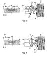
- FIG. 6 shows one of the FIG. 4 comparable vertical section together with individual elements of a resulting light distribution 20.
- Die FIG. 6 refers in particular to a direct imaging system with a five chips and thus five light emitting surfaces having semiconductor light source 12, which is imaged by a projection lens 16 in a light distribution 20 becomes.
- the light distribution 20 is thereby, as it also in connection with the FIG. 1b has already been explained, in an HV plane in front of the motor vehicle headlamp, wherein the horizontal axis H with the optical axis 28 and the vertical axis V forms a right-handed coordination system.
- FIG. 6 To explain the technical effects of the tilted arrangement, are in the FIG. 6 considered three different lens zones LZ1, LZ2 and LZ3. It is understood that this is a purely conceptual construction and that the lens could be divided into other lens zones in any manner.
- the lens zones can each be regarded as subregions of the main surface 18.
- a first lens zone LZ1 is arranged above the optical axis 28, while a second lens zone LZ2 is arranged in the region of the optical axis 28 and a third lens zone LZ3 below the optical axis 28.
- the upper lens zone LZ1 has a first distance S1 from the semiconductor light source 12 which is smaller than a distance S2 of the second lens zone LZ2 from the semiconductor light source 12, this distance S2 being smaller than a distance S3 the third lens zone LZ3 from the semiconductor light source 12.
- the different distances S1 less than S2 smaller S3 (S1 ⁇ S2 ⁇ S3) are due to the described inclination of the main surface 18 of the first projection lens 16.
- the lens zone LZ1 which has the five light exit surfaces Semiconductor light source 12 is closest, generates large images B_LZ1 the individual light exit surfaces of the semiconductor light source 12 in the light distribution 20.
- the lens zone LZ2 farther from the semiconductor light source 12 generates images B_LZ2 of Light exit surfaces of semiconductor chips Semiconductor light source 12, which are smaller than the images B_LZ1.
- the lens zone LZ3 farthest from the semiconductor light source 12 generates the smallest images B_LZ3 of the five light exit surfaces of the semiconductor chips of the semiconductor light source 12.
- the large images B_LZ1 are preferably used for the areas of light distribution in which large expansions and small illuminance levels are required, for example in the motor vehicle apron located close to the motor vehicle. With the associated lens zone LZ1 lying comparatively close to the semiconductor light source 12, a large amount of luminous flux can be absorbed and thus good optical efficiency can be achieved.
- smaller light source images for example the light source images B_LZ3 from lens zones LZ3 located farther away from the semiconductor light source 12, are well suited for illumination further ahead of the vehicle, which are just below the bright-dark boundary 26 in the light distribution 20. With these areas, the largest range is reached directly at the cut-off line 26, the larger range is purchased at a comparatively poor efficiency.
- the different lens zones merge into each other, so that their images in The light distribution 20 also overlap continuously from outside to inside or from inside to outside merging into each other. It is true that the largest chip images with the lowest illuminance come from the lens zone which is closest to the semiconductor light source 12, while the smallest chip images with the greatest illuminance come from the lens zone with the greatest distance to the semiconductor light source 12.
- the projection lens 16 is relative to Semiconductor light source 12 preferably positioned so that the semiconductor light source 12 is located in the Petzval surface of the vertical cross section of the projection lens 16, in which the optical axis 28 extends. This means that the light-dark boundary 26 is generated by the sharp image of the lower edge of the semiconductor light source 12. However, only individual areas from the vertical sections of the projection lens 16 contribute to the sharp imaging of the lower edge of the light source. The remaining edges of the light distribution 20 appear blurred, since the different lens zones each provide images of very different sizes. Since the horizontal section due to its opposite the vertical section other radius of curvature provides no sharp image, a horizontally wide-blazed light band is generated with low vertical extent, which is substantially less than the horizontal extent. This results qualitatively in the FIG. 1b illustrated form of light distribution 20th
- the projection lens 16 points to at least one lens surface, be it the Light entrance surface 48 and / or the light exit surface 54, at least partially scattering structures, the For example, realized by a wavy shape of the surface.
- scattering microstructures By means of such scattering microstructures, a slight blurring of the light-dark boundary can be achieved in a targeted manner, which contributes to the homogenization of the light distribution and, moreover, helps to eliminate chromatic aberrations.
- Vertically arranged cylindrical microlenses scatter horizontally and thus have no decisive influence on the illuminance gradient, that is to say on the maximum range of the headlamp 10.
- FIG. 7 shows an embodiment in which the optical system 14 in addition to the first projection lens 16 has a converging lens 60 which is disposed between the semiconductor light source 12 and the first projection lens 16. A part of the light emitted from the semiconductor light source 12 into the half-space passes through the condenser lens 60. This light is in the FIG. 7 represented by the opening angle 64. The portion 66 of the light emanating from the semiconductor light source 12, which passes through only the first projection lens 16 and does not pass through the condenser lens 60, generates small high-intensity light source images B_66, which are used to form the cut-off line 26.
- the additional converging lens 60 directs additional beams from the opening angle 64 onto the first projection lens 16 and thus increases the efficiency of the optical system.
- the quotient of the light emitted by the light source 12 in the denominator and of the light impinging in the light distribution 20 in the meter is understood here to be an efficiency or an efficiency of the optical system.
- the light 68 which is both the additional converging lens 60 and the first projection lens 16 has passed, appears to come from above the semiconductor light source 12. This means that the additional converging lens 60 generates virtual, enlarged images of the semiconductor light source 12, as shown as images B_68 in the light distribution 20 as shown in FIG FIG. 7 are shown. In the FIG. 7 this virtual extension is represented by a virtual image 62 of the semiconductor light source 12 lying above the semiconductor light source 12.
- the additional converging lens 60 is inclined upward to the semiconductor light source 12, while the first projection lens 16 is inclined upward from the first semiconductor light source 12 away. It is essential in any case that at least one of the two lenses 16, 60 has a defined according to the characterizing features of claim 1 inclination. It is this tendency that is responsible for the different magnifications. On the other hand, whether a larger magnification above the optical axis and a smaller magnification below the optical axis is generated, or whether a smaller magnification above the optical axis and a larger magnification below the optical axis is generated is of secondary importance.
- FIG. 8 shows a further embodiment, in which the additional converging lens is realized as a Fresnel lens with Fresnel zones 66.
- the additional converging lens is realized as a Fresnel lens with Fresnel zones 66.
- the light beams are deflected by a plurality of discrete Fresnel lens zones 66.
- the individual Fresnel lens zones 66 can be degenerated into prism wedges.
- FIG. 9 shows an embodiment in which the optical system 14 in addition to the first projection lens 16 has an additional reflector 68 which is disposed between the semiconductor light source 12 and the first projection lens 16.
- the additional reflector 68 is set up by its arrangement and its shape to direct light emanating from the semiconductor light source 12 through reflections occurring on at least one optical surface of the additional reflector 68 onto the light entrance surface 48 of the first projection lens 16 such that this light emerges next to the semiconductor light source 12, it appears that the luminous area of the semiconductor light source 12 is virtually widened in the vertical direction and / or in the horizontal direction.
- this virtual extension is represented by a virtual image 62 of the semiconductor light source 12 lying above the semiconductor light source 12.
- the additional reflector 68 has, in particular, a reflection surface arranged at an angle to the optical axis 28, so that light of the semiconductor light source 12 falling thereon is directed onto the light entry surface 48 of the first projection lens 16.
- the reflection surface can optionally be curved, in particular concavely arched.
- the additional reflector 68 is preferably arranged on at least one side edge of the semiconductor light source 12 such that a part of the light emitted by the semiconductor light source 12 falls on the additional reflector 68.
- the light exit surface of the semiconductor light source 12 is virtually enlarged.
- the reflected from the reflection surface of the additional reflector 68 rays appear from areas next to the Light exit surfaces of the chips of the semiconductor light source 12 to come and thus extend the images of the light exit surfaces of the chips of the semiconductor light source 12 in the resulting on the roadway light distribution 20 in front of the vehicle to the side or down. As a result, a soft outlet of the light distribution is achieved.
- a soft spout is understood here to mean a flat intensity gradient.
- the additional reflector 68 captures a luminous flux which would otherwise not strike the first projection lens 16 .
- the additional reflector 68 thus increases the total amount of light occurring on the light entry surface 48 of the first projection lens 16 and thus increases the optical efficiency.
- the auxiliary reflector 68 When the auxiliary reflector 68 is placed at the upper edge of the semiconductor light source 12, the light distribution 20 is extended downward in the direction of the vehicle apron, which is closer to the vehicle. If additional reflectors 68 are placed on the side edges of the semiconductor light source 12, the light distribution can then be expanded toward the sides with the aid of the additionally reflected light, thus improving the side illumination. As has already been explained in connection with the additional converging lens 60, here too the part of the light which only passes through the first projection lens 16 generates small light source images with high illuminance, which can be used for the formation of the cut-off line. The part of the light, which is directed by the additional reflector 68 to the projection lens 16, contributes to improved illumination of the great light source imagery, as in the FIG. 7 are denoted by the reference B_68.
- the reflection surface of the additional reflector 68 is realized in a preferred embodiment as a metallic coating of a forming and optionally with a painted to smooth roughness structure of the additional reflector 68.
- a reflective surface of the additional reflector 16 is realized as a white or diffusely reflecting surface.
- a white and / or diffuse reflective surface can be achieved, for example, by the reflective surface of the auxiliary reflector 68 comprising a layer containing titanium dioxide, zinc oxide, zinc sulfide, calcium carbonate, lead carbonate, barium sulfate or other white pigments.
- the additional reflector 68 may also be embodied as a reflector utilizing the effect of internal total reflection at an interface of a transparent solid and consisting, for example, of glass, PMMA (polymethyl methacrylate) or PC (polycarbonate).
- the reflection surface is formed by boundary surfaces of one or more deflection prisms, wherein such a deflection prism each having an optically active surface in the form of a refractive light entrance surface, a refractive light exit surface and at least one totally reflecting surface. All optically effective, that is to say the light direction changing surfaces can be convex or concave in this case.
- the additional reflector may have, at least in part, scattering, for example wavy, structures.
- the scattering structures can also be located on refracting light entry and exit surfaces.
- FIG. 9b shows an auxiliary reflector 68, which consists of a reflective coated and non-transparent structure.
- TIR Total Internal Reflection
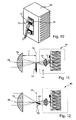
- the FIG. 10 shows a heat sink 38 with a mounted thereon circuit carrier 36, on the five LED Semiconductor chips are arranged, the one Represent semiconductor light source 12.
- the semiconductor light source 12 may also have a larger or smaller number n of semiconductor chips.
- the n semiconductor chips can be switched on and off independently of each other.
- the object of FIG. 10 is characterized by an aperture 70 arranged directly on the semiconductor light source 12, which sharply delimits a light bundle emanating from LED chips 72 of the semiconductor light source 12.
- the projection lens 16 images the semiconductor light source 12 with the aperture edge delimiting the light exit surface of the semiconductor light source 12 such that the light-dark boundary 26 results as an image of the diaphragm edge.
- This diaphragm edge creates a sharp cut-off line 26 in the light distribution 20 of a light module associated with the object of FIG. 10 Is provided.
- FIG. 11 shows an exemplary embodiment that has a light module 42, a diaphragm 74 and a second projection lens 76.
- the light module 42 corresponds to one of the embodiments described and explained up to here.
- Such a light module 42 has, in particular, a semiconductor light source 12 and an optical system 14 influencing the propagation direction of light of the semiconductor light source 12, which optical system has a first projection lens 16 with a main surface.
- the semiconductor light source 12 is disposed at a focal point of the first projection lens 16.
- the light module 42 is configured to produce a light distribution 20 having a bright area 22 and a dark area 24 separated from the bright area 22 by a horizontal cut-off line 26, and has an optical axis 28 which is a central point 30 of the cut-off line 26 connects to the semiconductor light source 12.
- the light module 42 is distinguished by the fact that the first projection lens 16 is arranged inclined relative to the optical axis 28 so that points 32 of the main surface 18 of the first projection lens 16 lie in a radial distance r from the optical axis 28 above the optical axis 28 Direction of the optical axis 28 have an axial distance d_32 to the semiconductor light source 12, which differs from an axial distance, the lying at the same radial distance r from the optical axis 28 below the optical axis 28 point 34 of the main surface 18 of the first projection lens sixteenth having.
- FIG. 11 illustrated embodiment differs from such a light module 42 by a second projection lens 76 in addition to the first projection lens 16 in the light path behind the first projection lens 16 arranged second projection lens 76.
- the embodiment shown in the FIG. 11 is configured to focus light emanating from the semiconductor light source 12 with the first projection lens 16 in a region which is at a distance of a focal length f of the second projection lens 76 from the second projection lens 76 between the first projection lens 16 and the second projection lens 76 ,
- the embodiment that is in the FIG. 11 is further configured to generate the light distribution projected onto the street as an image of an intermediate image mediated by the second projection lens 76, which image is formed from the light bundled in said area.
- the intermediate image is doing with one of the reference to the FIGS. 1 to 10 explained embodiments of a light module 42 generates.
- the intermediate image is additionally delimited by an aperture 74 introduced into the intermediate image plane, that is to say into the Petzval surface of the second projection lens 76, in order to achieve a particularly sharp cut-off line 26.
- the sharp cut-off line 26 is achieved in this case by the image of the intermediate image delimiting diaphragm edge.
- the second projection lens 76 focuses on the light distribution in the intermediate image plane 78 and images it with image reversal onto the road. With the edge of the aperture 74 projecting into the light distribution in the intermediate image plane, the light distribution in the intermediate image plane 78 is limited in order to achieve a sharper cut-off line.
- This panel 74 is realized as a mirror panel having a reflective surface 80.
- the aperture 74 with the reflective surface 80 is arranged so that the subject of the FIG. 11 on the first projection lens 16 side facing the aperture 74 falling light in the subject of FIG. 12 incident on the reflective surface 80 and is additionally directed by this on the light entry surface of the second projection lens 76.
- the one of the reflective surface 80 having aperture 74 from the Fig. 12 can therefore also be referred to as a mirror or mirror aperture.
- the second projection lens 76 facing the front edge of the aperture 74th lies in the Petzval area of the second projection lens or follows the course of the Petzval area of the second projection lens 76. Therefore, this mirror leading edge is sharply imaged by the second projection lens 76.
- the reflected rays are directed by the second projection lens 76 into an area below the cut-off line 26, where they amplify the light intensity.
- the leading edge of the mirror aperture 74 may be contoured to create a contoured cut-off line. In this case, the front mirror contour limits the light distribution in the intermediate image plane 78 so that a sharp cut-off line 26 is created.
- the first projection lens 16 and / or the condenser lens 60 and / or the second projection lens 76 and / or the reflector 68 on an optically active surface may have scattering structures. It is preferred that the scattering structures give the optically active surface a wavy shape. It is particularly preferred that the scattering structures have a shape of vertically arranged cylinder sections.
Landscapes
- Engineering & Computer Science (AREA)
- General Engineering & Computer Science (AREA)
- Physics & Mathematics (AREA)
- Microelectronics & Electronic Packaging (AREA)
- Optics & Photonics (AREA)
- Non-Portable Lighting Devices Or Systems Thereof (AREA)
Applications Claiming Priority (1)
| Application Number | Priority Date | Filing Date | Title |
|---|---|---|---|
| DE102011006380A DE102011006380A1 (de) | 2011-03-29 | 2011-03-29 | Kraftfahrzeugscheinwerfer mit einer Halbleiterlichtquelle |
Publications (3)
| Publication Number | Publication Date |
|---|---|
| EP2505910A2 true EP2505910A2 (fr) | 2012-10-03 |
| EP2505910A3 EP2505910A3 (fr) | 2013-08-28 |
| EP2505910B1 EP2505910B1 (fr) | 2019-11-13 |
Family
ID=45954390
Family Applications (1)
| Application Number | Title | Priority Date | Filing Date |
|---|---|---|---|
| EP12161419.2A Active EP2505910B1 (fr) | 2011-03-29 | 2012-03-27 | Phare de véhicule automobile équipé d'une source lumineuse semi-conductrice |
Country Status (3)
| Country | Link |
|---|---|
| EP (1) | EP2505910B1 (fr) |
| CN (1) | CN102734732B (fr) |
| DE (1) | DE102011006380A1 (fr) |
Cited By (7)
| Publication number | Priority date | Publication date | Assignee | Title |
|---|---|---|---|---|
| WO2015191387A1 (fr) * | 2014-06-08 | 2015-12-17 | Valeo North America, Inc. | Système d'éclairage à réflecteur et lentille générant un diagramme de lumière avec ligne de coupure |
| EP2796773A3 (fr) * | 2013-04-22 | 2018-01-03 | Koito Manufacturing Co., Ltd. | Phare de véhicule |
| WO2018019397A1 (fr) * | 2016-07-27 | 2018-02-01 | Docter Optics Se | Lentille de projecteur pour projecteur de véhicule à moteur |
| EP3470728A1 (fr) * | 2017-10-16 | 2019-04-17 | Valeo Vision | Module lumineux pour vehicule automobile |
| EP3719391A1 (fr) * | 2019-03-29 | 2020-10-07 | Marelli Automotive Lighting Reutlingen (Germany) GmbH | Module de feu de route partiel pour un phare de véhicule automobile |
| EP3839324A1 (fr) * | 2019-12-16 | 2021-06-23 | ZKW Group GmbH | Dispositif d'éclairage pour un phare de véhicule automobile |
| CN113037968A (zh) * | 2021-03-01 | 2021-06-25 | 维沃移动通信有限公司 | 电子设备 |
Families Citing this family (5)
| Publication number | Priority date | Publication date | Assignee | Title |
|---|---|---|---|---|
| KR101847932B1 (ko) * | 2015-04-23 | 2018-04-11 | 엘지전자 주식회사 | 발광모듈 |
| JP6595881B2 (ja) * | 2015-10-27 | 2019-10-23 | スタンレー電気株式会社 | 拡散配光光学系及び車両用灯具 |
| JP7002255B2 (ja) * | 2017-09-08 | 2022-02-04 | スタンレー電気株式会社 | 車両用灯具 |
| DE102017128125B4 (de) * | 2017-11-28 | 2024-02-22 | OSRAM Opto Semiconductors Gesellschaft mit beschränkter Haftung | Scheinwerfer und Betriebsverfahren |
| KR102454229B1 (ko) | 2020-11-30 | 2022-10-14 | 현대모비스 주식회사 | 차량용 램프 |
Family Cites Families (11)
| Publication number | Priority date | Publication date | Assignee | Title |
|---|---|---|---|---|
| GB496885A (en) * | 1936-07-27 | 1938-12-07 | Research Corp | Improvements in light projecting systems |
| JPH05266701A (ja) * | 1992-03-18 | 1993-10-15 | Nippondenso Co Ltd | 車両用前照灯装置 |
| JP2003123519A (ja) * | 2001-10-15 | 2003-04-25 | Honda Motor Co Ltd | プロジェクタ型ヘッドランプ |
| JP4024721B2 (ja) * | 2003-06-20 | 2007-12-19 | 株式会社小糸製作所 | 車両用灯具及び光源モジュール |
| JP2006049190A (ja) * | 2004-08-06 | 2006-02-16 | Koito Mfg Co Ltd | 車両用前照灯 |
| JP4536483B2 (ja) * | 2004-10-27 | 2010-09-01 | 株式会社小糸製作所 | 車両用照明灯具 |
| AT504505B1 (de) * | 2006-10-23 | 2008-06-15 | Zizala Lichtsysteme Gmbh | Optikelement für einen fahrzeugscheinwerfer |
| DE102007007943A1 (de) * | 2007-02-17 | 2008-08-21 | Daimler Ag | Lichteinheit, insbesondere Scheinwerfer, für ein Fahrzeug |
| JP4970136B2 (ja) * | 2007-05-17 | 2012-07-04 | 株式会社小糸製作所 | 車両用前照灯の灯具ユニット |
| JP4582190B2 (ja) * | 2008-05-14 | 2010-11-17 | 市光工業株式会社 | 車両用灯具 |
| JP5257665B2 (ja) * | 2008-08-20 | 2013-08-07 | スタンレー電気株式会社 | 車両用前照灯ユニット及び車両用前照灯 |
-
2011
- 2011-03-29 DE DE102011006380A patent/DE102011006380A1/de not_active Withdrawn
-
2012
- 2012-03-27 EP EP12161419.2A patent/EP2505910B1/fr active Active
- 2012-03-28 CN CN201210086700.8A patent/CN102734732B/zh not_active Expired - Fee Related
Non-Patent Citations (1)
| Title |
|---|
| None |
Cited By (15)
| Publication number | Priority date | Publication date | Assignee | Title |
|---|---|---|---|---|
| EP2796773A3 (fr) * | 2013-04-22 | 2018-01-03 | Koito Manufacturing Co., Ltd. | Phare de véhicule |
| US11221119B2 (en) | 2014-06-08 | 2022-01-11 | Valeo North America, Inc. | Thin aspect lighting system with cutoff |
| US10697607B2 (en) | 2014-06-08 | 2020-06-30 | Valeo North America, Inc. | Thin aspect lighting system with cutoff |
| WO2015191387A1 (fr) * | 2014-06-08 | 2015-12-17 | Valeo North America, Inc. | Système d'éclairage à réflecteur et lentille générant un diagramme de lumière avec ligne de coupure |
| US11686446B2 (en) | 2014-06-08 | 2023-06-27 | Valeo North America, Inc. | Thin aspect lighting system with cutoff |
| US11384912B2 (en) | 2014-06-08 | 2022-07-12 | Valeo North America, Inc. | Thin aspect lighting system with cutoff |
| WO2018019397A1 (fr) * | 2016-07-27 | 2018-02-01 | Docter Optics Se | Lentille de projecteur pour projecteur de véhicule à moteur |
| EP3470728A1 (fr) * | 2017-10-16 | 2019-04-17 | Valeo Vision | Module lumineux pour vehicule automobile |
| FR3072445A1 (fr) * | 2017-10-16 | 2019-04-19 | Valeo Vision | Module lumineux pour vehicule automobile |
| US10837613B2 (en) | 2017-10-16 | 2020-11-17 | Valeo Vision | Lighting module having a flexible matrix coinciding with the first object focal surface of the imaging device |
| EP3719391A1 (fr) * | 2019-03-29 | 2020-10-07 | Marelli Automotive Lighting Reutlingen (Germany) GmbH | Module de feu de route partiel pour un phare de véhicule automobile |
| WO2021122565A1 (fr) * | 2019-12-16 | 2021-06-24 | Zkw Group Gmbh | Dispositif d'éclairage pour phare de véhicule automobile |
| US11447066B2 (en) | 2019-12-16 | 2022-09-20 | Zkw Group Gmbh | Lighting device for a motor vehicle headlight |
| EP3839324A1 (fr) * | 2019-12-16 | 2021-06-23 | ZKW Group GmbH | Dispositif d'éclairage pour un phare de véhicule automobile |
| CN113037968A (zh) * | 2021-03-01 | 2021-06-25 | 维沃移动通信有限公司 | 电子设备 |
Also Published As
| Publication number | Publication date |
|---|---|
| EP2505910A3 (fr) | 2013-08-28 |
| EP2505910B1 (fr) | 2019-11-13 |
| CN102734732B (zh) | 2016-08-31 |
| CN102734732A (zh) | 2012-10-17 |
| DE102011006380A1 (de) | 2012-10-04 |
Similar Documents
| Publication | Publication Date | Title |
|---|---|---|
| EP2505910B1 (fr) | Phare de véhicule automobile équipé d'une source lumineuse semi-conductrice | |
| EP2910847B1 (fr) | Module d'éclairage d'un projecteur de véhicule automobile et projecteur avec un tel module d'éclairage | |
| DE102012202290B4 (de) | Lichtmodul für ein blendungsfreies Kraftfahrzeug-Fernlicht | |
| EP2799762B1 (fr) | Module d'éclairage de phare de véhicule automobile | |
| DE102009053581B3 (de) | Lichtmodul für eine Beleuchtungseinrichtung eines Kraftfahrzeugs | |
| EP2587125B1 (fr) | Module de projection de phare pour un véhicule automobile | |
| DE102004043706B4 (de) | Optisches System für einen Kraftfahrzeugscheinwerfer, Beleuchtungseinheit für einen Kraftfahrzeugscheinwerfer und Kraftfahrzeugscheinwerfer | |
| EP2306074B1 (fr) | Phare de véhicule automobile doté d'un module d'éclairage comprenant des sources de lumière à semi-conducteurs, une optique primaire et une optique secondaire | |
| DE102008051109B4 (de) | Kraftfahrzeugscheinwerfer und Verfahren zur Herstellung eines Kraftfahrzeugscheinwerfers | |
| DE102014200368B4 (de) | Teilfernlicht-Projektionslichtmodul für einen Kraftfahrzeugscheinwerfer | |
| WO2011154470A1 (fr) | Accessoire optique constitué d'un matériau transparent pour la focalisation de lumière, ensemble de lentilles comportant au moins un tel accessoire optique, et module de lumière doté d'un tel ensemble de lentilles | |
| WO2012119976A1 (fr) | Projecteur de véhicule automobile équipé d'un module de projection multifonction | |
| DE102017205010A1 (de) | Fahrzeugleuchte und Fahrzeug mit einer solchen | |
| DE102009037698A1 (de) | Fahrzeugbeleuchtungseinheit und Fahrzeugleuchte | |
| DE102011078653B4 (de) | Vorsatzoptik zur Bündelung von ausgesandtem Licht mindestens einer Halbleiterlichtquelle | |
| EP2799761A2 (fr) | Module d'éclairage de phare de véhicule automobile | |
| DE102015224745B4 (de) | Kraftfahrzeugscheinwerfer mit einer Grundlichtbaugruppe und einer Fernlichtbaugruppe | |
| EP1818600B1 (fr) | Feu de croisement doté d'une production d'un point chaud | |
| EP2789901A2 (fr) | Module d'éclairage pour un dispositif d'éclairage de véhicule automobile | |
| EP3301350B1 (fr) | Module d'éclairage pour phare de véhicule automobile | |
| EP1818599A2 (fr) | Feu de croisement, produisant une coupure à contraste importante | |
| EP2523022A1 (fr) | Module d'éclairage pour un phare de véhicule automobile destiné à la production d'une distribution lumineuse variable et phare de véhicule automobile doté d'un tel module d'éclairage | |
| DE102012220507A1 (de) | Lichtmodul für einen Scheinwerfer eines Kraftfahrzeugs | |
| DE102017107781A1 (de) | Primäroptikeinheit für ein Lichtmodul | |
| DE102013215359B3 (de) | Mechanikfreies Kurvenlichtmodul |
Legal Events
| Date | Code | Title | Description |
|---|---|---|---|
| PUAI | Public reference made under article 153(3) epc to a published international application that has entered the european phase |
Free format text: ORIGINAL CODE: 0009012 |
|
| AK | Designated contracting states |
Kind code of ref document: A2 Designated state(s): AL AT BE BG CH CY CZ DE DK EE ES FI FR GB GR HR HU IE IS IT LI LT LU LV MC MK MT NL NO PL PT RO RS SE SI SK SM TR |
|
| AX | Request for extension of the european patent |
Extension state: BA ME |
|
| PUAL | Search report despatched |
Free format text: ORIGINAL CODE: 0009013 |
|
| AK | Designated contracting states |
Kind code of ref document: A3 Designated state(s): AL AT BE BG CH CY CZ DE DK EE ES FI FR GB GR HR HU IE IS IT LI LT LU LV MC MK MT NL NO PL PT RO RS SE SI SK SM TR |
|
| AX | Request for extension of the european patent |
Extension state: BA ME |
|
| RIC1 | Information provided on ipc code assigned before grant |
Ipc: F21V 1/00 20060101ALI20130719BHEP Ipc: F21V 5/00 20060101ALI20130719BHEP Ipc: F21V 7/00 20060101ALI20130719BHEP Ipc: F21V 11/16 20060101ALI20130719BHEP Ipc: F21S 8/12 20060101AFI20130719BHEP |
|
| 17P | Request for examination filed |
Effective date: 20140211 |
|
| RBV | Designated contracting states (corrected) |
Designated state(s): AL AT BE BG CH CY CZ DE DK EE ES FI FR GB GR HR HU IE IS IT LI LT LU LV MC MK MT NL NO PL PT RO RS SE SI SK SM TR |
|
| STAA | Information on the status of an ep patent application or granted ep patent |
Free format text: STATUS: EXAMINATION IS IN PROGRESS |
|
| 17Q | First examination report despatched |
Effective date: 20161118 |
|
| REG | Reference to a national code |
Ref country code: DE Ref legal event code: R079 Ref document number: 502012015515 Country of ref document: DE Free format text: PREVIOUS MAIN CLASS: F21S0008120000 Ipc: F21S0041260000 |
|
| RIC1 | Information provided on ipc code assigned before grant |
Ipc: F21S 41/32 20180101ALI20190321BHEP Ipc: F21S 41/143 20180101ALI20190321BHEP Ipc: F21S 41/20 20180101ALI20190321BHEP Ipc: F21S 41/26 20180101AFI20190321BHEP |
|
| GRAP | Despatch of communication of intention to grant a patent |
Free format text: ORIGINAL CODE: EPIDOSNIGR1 |
|
| STAA | Information on the status of an ep patent application or granted ep patent |
Free format text: STATUS: GRANT OF PATENT IS INTENDED |
|
| INTG | Intention to grant announced |
Effective date: 20190523 |
|
| GRAS | Grant fee paid |
Free format text: ORIGINAL CODE: EPIDOSNIGR3 |
|
| GRAA | (expected) grant |
Free format text: ORIGINAL CODE: 0009210 |
|
| STAA | Information on the status of an ep patent application or granted ep patent |
Free format text: STATUS: THE PATENT HAS BEEN GRANTED |
|
| AK | Designated contracting states |
Kind code of ref document: B1 Designated state(s): AL AT BE BG CH CY CZ DE DK EE ES FI FR GB GR HR HU IE IS IT LI LT LU LV MC MK MT NL NO PL PT RO RS SE SI SK SM TR |
|
| REG | Reference to a national code |
Ref country code: CH Ref legal event code: EP Ref country code: AT Ref legal event code: REF Ref document number: 1202030 Country of ref document: AT Kind code of ref document: T Effective date: 20191115 |
|
| REG | Reference to a national code |
Ref country code: DE Ref legal event code: R096 Ref document number: 502012015515 Country of ref document: DE |
|
| REG | Reference to a national code |
Ref country code: IE Ref legal event code: FG4D Free format text: LANGUAGE OF EP DOCUMENT: GERMAN |
|
| REG | Reference to a national code |
Ref country code: NL Ref legal event code: MP Effective date: 20191113 |
|
| REG | Reference to a national code |
Ref country code: LT Ref legal event code: MG4D |
|
| PG25 | Lapsed in a contracting state [announced via postgrant information from national office to epo] |
Ref country code: PL Free format text: LAPSE BECAUSE OF FAILURE TO SUBMIT A TRANSLATION OF THE DESCRIPTION OR TO PAY THE FEE WITHIN THE PRESCRIBED TIME-LIMIT Effective date: 20191113 Ref country code: NL Free format text: LAPSE BECAUSE OF FAILURE TO SUBMIT A TRANSLATION OF THE DESCRIPTION OR TO PAY THE FEE WITHIN THE PRESCRIBED TIME-LIMIT Effective date: 20191113 Ref country code: SE Free format text: LAPSE BECAUSE OF FAILURE TO SUBMIT A TRANSLATION OF THE DESCRIPTION OR TO PAY THE FEE WITHIN THE PRESCRIBED TIME-LIMIT Effective date: 20191113 Ref country code: LT Free format text: LAPSE BECAUSE OF FAILURE TO SUBMIT A TRANSLATION OF THE DESCRIPTION OR TO PAY THE FEE WITHIN THE PRESCRIBED TIME-LIMIT Effective date: 20191113 Ref country code: BG Free format text: LAPSE BECAUSE OF FAILURE TO SUBMIT A TRANSLATION OF THE DESCRIPTION OR TO PAY THE FEE WITHIN THE PRESCRIBED TIME-LIMIT Effective date: 20200213 Ref country code: ES Free format text: LAPSE BECAUSE OF FAILURE TO SUBMIT A TRANSLATION OF THE DESCRIPTION OR TO PAY THE FEE WITHIN THE PRESCRIBED TIME-LIMIT Effective date: 20191113 Ref country code: FI Free format text: LAPSE BECAUSE OF FAILURE TO SUBMIT A TRANSLATION OF THE DESCRIPTION OR TO PAY THE FEE WITHIN THE PRESCRIBED TIME-LIMIT Effective date: 20191113 Ref country code: GR Free format text: LAPSE BECAUSE OF FAILURE TO SUBMIT A TRANSLATION OF THE DESCRIPTION OR TO PAY THE FEE WITHIN THE PRESCRIBED TIME-LIMIT Effective date: 20200214 Ref country code: LV Free format text: LAPSE BECAUSE OF FAILURE TO SUBMIT A TRANSLATION OF THE DESCRIPTION OR TO PAY THE FEE WITHIN THE PRESCRIBED TIME-LIMIT Effective date: 20191113 Ref country code: NO Free format text: LAPSE BECAUSE OF FAILURE TO SUBMIT A TRANSLATION OF THE DESCRIPTION OR TO PAY THE FEE WITHIN THE PRESCRIBED TIME-LIMIT Effective date: 20200213 Ref country code: PT Free format text: LAPSE BECAUSE OF FAILURE TO SUBMIT A TRANSLATION OF THE DESCRIPTION OR TO PAY THE FEE WITHIN THE PRESCRIBED TIME-LIMIT Effective date: 20200313 |
|
| PG25 | Lapsed in a contracting state [announced via postgrant information from national office to epo] |
Ref country code: IS Free format text: LAPSE BECAUSE OF FAILURE TO SUBMIT A TRANSLATION OF THE DESCRIPTION OR TO PAY THE FEE WITHIN THE PRESCRIBED TIME-LIMIT Effective date: 20200313 Ref country code: HR Free format text: LAPSE BECAUSE OF FAILURE TO SUBMIT A TRANSLATION OF THE DESCRIPTION OR TO PAY THE FEE WITHIN THE PRESCRIBED TIME-LIMIT Effective date: 20191113 Ref country code: RS Free format text: LAPSE BECAUSE OF FAILURE TO SUBMIT A TRANSLATION OF THE DESCRIPTION OR TO PAY THE FEE WITHIN THE PRESCRIBED TIME-LIMIT Effective date: 20191113 |
|
| PG25 | Lapsed in a contracting state [announced via postgrant information from national office to epo] |
Ref country code: AL Free format text: LAPSE BECAUSE OF FAILURE TO SUBMIT A TRANSLATION OF THE DESCRIPTION OR TO PAY THE FEE WITHIN THE PRESCRIBED TIME-LIMIT Effective date: 20191113 |
|
| PG25 | Lapsed in a contracting state [announced via postgrant information from national office to epo] |
Ref country code: EE Free format text: LAPSE BECAUSE OF FAILURE TO SUBMIT A TRANSLATION OF THE DESCRIPTION OR TO PAY THE FEE WITHIN THE PRESCRIBED TIME-LIMIT Effective date: 20191113 Ref country code: CZ Free format text: LAPSE BECAUSE OF FAILURE TO SUBMIT A TRANSLATION OF THE DESCRIPTION OR TO PAY THE FEE WITHIN THE PRESCRIBED TIME-LIMIT Effective date: 20191113 Ref country code: RO Free format text: LAPSE BECAUSE OF FAILURE TO SUBMIT A TRANSLATION OF THE DESCRIPTION OR TO PAY THE FEE WITHIN THE PRESCRIBED TIME-LIMIT Effective date: 20191113 Ref country code: DK Free format text: LAPSE BECAUSE OF FAILURE TO SUBMIT A TRANSLATION OF THE DESCRIPTION OR TO PAY THE FEE WITHIN THE PRESCRIBED TIME-LIMIT Effective date: 20191113 |
|
| REG | Reference to a national code |
Ref country code: DE Ref legal event code: R097 Ref document number: 502012015515 Country of ref document: DE |
|
| PG25 | Lapsed in a contracting state [announced via postgrant information from national office to epo] |
Ref country code: SK Free format text: LAPSE BECAUSE OF FAILURE TO SUBMIT A TRANSLATION OF THE DESCRIPTION OR TO PAY THE FEE WITHIN THE PRESCRIBED TIME-LIMIT Effective date: 20191113 Ref country code: SM Free format text: LAPSE BECAUSE OF FAILURE TO SUBMIT A TRANSLATION OF THE DESCRIPTION OR TO PAY THE FEE WITHIN THE PRESCRIBED TIME-LIMIT Effective date: 20191113 |
|
| PLBE | No opposition filed within time limit |
Free format text: ORIGINAL CODE: 0009261 |
|
| STAA | Information on the status of an ep patent application or granted ep patent |
Free format text: STATUS: NO OPPOSITION FILED WITHIN TIME LIMIT |
|
| 26N | No opposition filed |
Effective date: 20200814 |
|
| PG25 | Lapsed in a contracting state [announced via postgrant information from national office to epo] |
Ref country code: MC Free format text: LAPSE BECAUSE OF FAILURE TO SUBMIT A TRANSLATION OF THE DESCRIPTION OR TO PAY THE FEE WITHIN THE PRESCRIBED TIME-LIMIT Effective date: 20191113 |
|
| REG | Reference to a national code |
Ref country code: CH Ref legal event code: PL |
|
| PG25 | Lapsed in a contracting state [announced via postgrant information from national office to epo] |
Ref country code: SI Free format text: LAPSE BECAUSE OF FAILURE TO SUBMIT A TRANSLATION OF THE DESCRIPTION OR TO PAY THE FEE WITHIN THE PRESCRIBED TIME-LIMIT Effective date: 20191113 |
|
| REG | Reference to a national code |
Ref country code: BE Ref legal event code: MM Effective date: 20200331 |
|
| PG25 | Lapsed in a contracting state [announced via postgrant information from national office to epo] |
Ref country code: LU Free format text: LAPSE BECAUSE OF NON-PAYMENT OF DUE FEES Effective date: 20200327 |
|
| PG25 | Lapsed in a contracting state [announced via postgrant information from national office to epo] |
Ref country code: CH Free format text: LAPSE BECAUSE OF NON-PAYMENT OF DUE FEES Effective date: 20200331 Ref country code: FR Free format text: LAPSE BECAUSE OF NON-PAYMENT OF DUE FEES Effective date: 20200331 Ref country code: IT Free format text: LAPSE BECAUSE OF FAILURE TO SUBMIT A TRANSLATION OF THE DESCRIPTION OR TO PAY THE FEE WITHIN THE PRESCRIBED TIME-LIMIT Effective date: 20191113 Ref country code: IE Free format text: LAPSE BECAUSE OF NON-PAYMENT OF DUE FEES Effective date: 20200327 Ref country code: LI Free format text: LAPSE BECAUSE OF NON-PAYMENT OF DUE FEES Effective date: 20200331 |
|
| PG25 | Lapsed in a contracting state [announced via postgrant information from national office to epo] |
Ref country code: BE Free format text: LAPSE BECAUSE OF NON-PAYMENT OF DUE FEES Effective date: 20200331 |
|
| GBPC | Gb: european patent ceased through non-payment of renewal fee |
Effective date: 20200327 |
|
| PG25 | Lapsed in a contracting state [announced via postgrant information from national office to epo] |
Ref country code: GB Free format text: LAPSE BECAUSE OF NON-PAYMENT OF DUE FEES Effective date: 20200327 |
|
| REG | Reference to a national code |
Ref country code: AT Ref legal event code: MM01 Ref document number: 1202030 Country of ref document: AT Kind code of ref document: T Effective date: 20200327 |
|
| PG25 | Lapsed in a contracting state [announced via postgrant information from national office to epo] |
Ref country code: AT Free format text: LAPSE BECAUSE OF NON-PAYMENT OF DUE FEES Effective date: 20200327 |
|
| PG25 | Lapsed in a contracting state [announced via postgrant information from national office to epo] |
Ref country code: TR Free format text: LAPSE BECAUSE OF FAILURE TO SUBMIT A TRANSLATION OF THE DESCRIPTION OR TO PAY THE FEE WITHIN THE PRESCRIBED TIME-LIMIT Effective date: 20191113 Ref country code: MT Free format text: LAPSE BECAUSE OF FAILURE TO SUBMIT A TRANSLATION OF THE DESCRIPTION OR TO PAY THE FEE WITHIN THE PRESCRIBED TIME-LIMIT Effective date: 20191113 Ref country code: CY Free format text: LAPSE BECAUSE OF FAILURE TO SUBMIT A TRANSLATION OF THE DESCRIPTION OR TO PAY THE FEE WITHIN THE PRESCRIBED TIME-LIMIT Effective date: 20191113 |
|
| PG25 | Lapsed in a contracting state [announced via postgrant information from national office to epo] |
Ref country code: MK Free format text: LAPSE BECAUSE OF FAILURE TO SUBMIT A TRANSLATION OF THE DESCRIPTION OR TO PAY THE FEE WITHIN THE PRESCRIBED TIME-LIMIT Effective date: 20191113 |
|
| PGFP | Annual fee paid to national office [announced via postgrant information from national office to epo] |
Ref country code: DE Payment date: 20230221 Year of fee payment: 12 |
|
| REG | Reference to a national code |
Ref country code: DE Ref legal event code: R084 Ref document number: 502012015515 Country of ref document: DE |