EP2492957A2 - Schaltungsanordnung - Google Patents
Schaltungsanordnung Download PDFInfo
- Publication number
- EP2492957A2 EP2492957A2 EP12150873A EP12150873A EP2492957A2 EP 2492957 A2 EP2492957 A2 EP 2492957A2 EP 12150873 A EP12150873 A EP 12150873A EP 12150873 A EP12150873 A EP 12150873A EP 2492957 A2 EP2492957 A2 EP 2492957A2
- Authority
- EP
- European Patent Office
- Prior art keywords
- metal layer
- edge
- circuit arrangement
- rounding
- insulating material
- Prior art date
- Legal status (The legal status is an assumption and is not a legal conclusion. Google has not performed a legal analysis and makes no representation as to the accuracy of the status listed.)
- Granted
Links
Images


Classifications
-
- H—ELECTRICITY
- H10—SEMICONDUCTOR DEVICES; ELECTRIC SOLID-STATE DEVICES NOT OTHERWISE PROVIDED FOR
- H10W—GENERIC PACKAGES, INTERCONNECTIONS, CONNECTORS OR OTHER CONSTRUCTIONAL DETAILS OF DEVICES COVERED BY CLASS H10
- H10W76/00—Containers; Fillings or auxiliary members therefor; Seals
- H10W76/40—Fillings or auxiliary members in containers, e.g. centering rings
- H10W76/42—Fillings
- H10W76/47—Solid or gel fillings
-
- H—ELECTRICITY
- H10—SEMICONDUCTOR DEVICES; ELECTRIC SOLID-STATE DEVICES NOT OTHERWISE PROVIDED FOR
- H10W—GENERIC PACKAGES, INTERCONNECTIONS, CONNECTORS OR OTHER CONSTRUCTIONAL DETAILS OF DEVICES COVERED BY CLASS H10
- H10W70/00—Package substrates; Interposers; Redistribution layers [RDL]
- H10W70/60—Insulating or insulated package substrates; Interposers; Redistribution layers
-
- H—ELECTRICITY
- H10—SEMICONDUCTOR DEVICES; ELECTRIC SOLID-STATE DEVICES NOT OTHERWISE PROVIDED FOR
- H10W—GENERIC PACKAGES, INTERCONNECTIONS, CONNECTORS OR OTHER CONSTRUCTIONAL DETAILS OF DEVICES COVERED BY CLASS H10
- H10W72/00—Interconnections or connectors in packages
-
- H—ELECTRICITY
- H10—SEMICONDUCTOR DEVICES; ELECTRIC SOLID-STATE DEVICES NOT OTHERWISE PROVIDED FOR
- H10W—GENERIC PACKAGES, INTERCONNECTIONS, CONNECTORS OR OTHER CONSTRUCTIONAL DETAILS OF DEVICES COVERED BY CLASS H10
- H10W90/00—Package configurations
-
- H—ELECTRICITY
- H10—SEMICONDUCTOR DEVICES; ELECTRIC SOLID-STATE DEVICES NOT OTHERWISE PROVIDED FOR
- H10W—GENERIC PACKAGES, INTERCONNECTIONS, CONNECTORS OR OTHER CONSTRUCTIONAL DETAILS OF DEVICES COVERED BY CLASS H10
- H10W72/00—Interconnections or connectors in packages
- H10W72/50—Bond wires
- H10W72/531—Shapes of wire connectors
- H10W72/5363—Shapes of wire connectors the connected ends being wedge-shaped
-
- H—ELECTRICITY
- H10—SEMICONDUCTOR DEVICES; ELECTRIC SOLID-STATE DEVICES NOT OTHERWISE PROVIDED FOR
- H10W—GENERIC PACKAGES, INTERCONNECTIONS, CONNECTORS OR OTHER CONSTRUCTIONAL DETAILS OF DEVICES COVERED BY CLASS H10
- H10W72/00—Interconnections or connectors in packages
- H10W72/50—Bond wires
- H10W72/541—Dispositions of bond wires
- H10W72/5438—Dispositions of bond wires the bond wires having multiple connections on the same bond pad
-
- H—ELECTRICITY
- H10—SEMICONDUCTOR DEVICES; ELECTRIC SOLID-STATE DEVICES NOT OTHERWISE PROVIDED FOR
- H10W—GENERIC PACKAGES, INTERCONNECTIONS, CONNECTORS OR OTHER CONSTRUCTIONAL DETAILS OF DEVICES COVERED BY CLASS H10
- H10W72/00—Interconnections or connectors in packages
- H10W72/50—Bond wires
- H10W72/541—Dispositions of bond wires
- H10W72/5453—Dispositions of bond wires connecting between multiple bond pads on a chip, e.g. daisy chain
-
- H—ELECTRICITY
- H10—SEMICONDUCTOR DEVICES; ELECTRIC SOLID-STATE DEVICES NOT OTHERWISE PROVIDED FOR
- H10W—GENERIC PACKAGES, INTERCONNECTIONS, CONNECTORS OR OTHER CONSTRUCTIONAL DETAILS OF DEVICES COVERED BY CLASS H10
- H10W74/00—Encapsulations, e.g. protective coatings
-
- H—ELECTRICITY
- H10—SEMICONDUCTOR DEVICES; ELECTRIC SOLID-STATE DEVICES NOT OTHERWISE PROVIDED FOR
- H10W—GENERIC PACKAGES, INTERCONNECTIONS, CONNECTORS OR OTHER CONSTRUCTIONAL DETAILS OF DEVICES COVERED BY CLASS H10
- H10W90/00—Package configurations
- H10W90/701—Package configurations characterised by the relative positions of pads or connectors relative to package parts
- H10W90/751—Package configurations characterised by the relative positions of pads or connectors relative to package parts of bond wires
- H10W90/754—Package configurations characterised by the relative positions of pads or connectors relative to package parts of bond wires between a chip and a stacked insulating package substrate, interposer or RDL
Definitions
- the invention relates to a circuit arrangement with an insulating body, which has a schaltGermaniert metal layer and at least one attached thereto power semiconductor device on a main surface, and with a mounted on the insulating body, the contour of the insulating material with the attached thereto at least one power semiconductor device layer of an insulating material.
- Such a circuit arrangement is known from DE 10 2004 021 927 B4 known.
- a viscous dielectric insulating material In the insulation of this known circuit arrangement is a viscous dielectric insulating material, wherein after the application of the viscous dielectric insulating material, a cross-linking thereof is initiated. Subsequently, a rotation of the insulating material takes place about an axis perpendicular to its vertical axis, so that the viscous dielectric insulating material encloses the circuit formed by bonding wire connections of the at least one power semiconductor device and excess viscous insulating mass gravitationally drips from Isolierstoff emotions.
- the provided with the insulating material layer insulating material is placed in a housing, after which a complete crosslinking of the dielectric insulating material takes place, resulting in an adhesive bond between the housing and the insulating body.
- the invention has for its object to provide a circuit arrangement of the type mentioned, with an unwanted interruption of the insulation cover is prevented in a simple manner.
- the casting material for the perineum bead a defined space on the Isolierstoff emotions commanded, ie ensures a secure positioning of Dammwulst Vergußmaterials so that the potting material for the perineum does not drip unintentionally over the peripheral edge of the insulating material.
- the insulation material layer is defined by the dam bead defined and prevented from dripping over the edge of the insulating material. An unwanted detachment of the insulating material layer is prevented according to the invention, so that a disruption of the insulation cover, which would lead to insulation weak points and in extreme cases to a failure of the circuit arrangement is avoided in a simple manner.
- the schalt Vietnamese metal layer and the metal layer frame are preferably made of the same metal, for example. Of copper, or of the same metal alloy.
- the insulator body consists, for example, of an industrial ceramic such as Al 2 O 3 or the like.
- the trench which separates the metal layer frame from the edge of the adjacent shell-structured metal layer preferably extends as far as the associated main surface of the insulating body, for example by etching the metal layer provided on the corresponding main surface of the insulating body simultaneously with the switching patterning thereof.
- the metal layer frame is formed in its longitudinal extension with recesses spaced apart from one another.
- the depressions can be produced by etching, simultaneously with the production of the trench.
- the metal layer frame may extend to the peripheral edge of the insulating material or have a defined distance from the edge of the insulating material to glue a housing of the circuit arrangement by means of the dam with the Isolierstoff stresses or to define the circumferential dam bead defined by the housing of the circuit arrangement.
- the dam bead is usually applied to the insulating body by means of a nozzle device.
- the nozzle device In the region of the respective corner of the insulating material, the nozzle device is for production reasons, but not stopped for productivity reasons, to effect a conversion of the nozzle device from the one spatial direction in the spatial direction perpendicular thereto, but the nozzle device moves in the respective corner region of the insulating material along a rounded path with a small radius of curvature.
- the edge of the circuit-structured metal layer of the circuit arrangement in the region of the respective corner of the insulating material body is formed with a sharp-edged right-angled corner, a reduction in the isolation distance between results from the rounded profile of the dam bead the corner of the schalt Vietnamese striving metal layer and the outer edge of the dam.
- This reduction of the isolation distance can have an adverse effect on the insulation resistance.
- the dam bead runs rounded in the respective corner region of the insulating body, and the edge of the shell-structured metal layer is formed in the respective corner region of the shell-structured metal layer with a rounding or with a chamfer. It is advantageous if the rounding or the chamfering of the edge of the shell-structured metal layer is adapted to the formed in the respective corner region of the insulating body rounding of Dammwulstes.
- the dam bead runs rounded in the respective corner region of the insulating material, and if the metal layer frame has an inner edge which is formed in the respective corner region of the insulating material with a rounding or with a chamfer.
- the rounding or the chamfering of the inner edge of the metal layer frame is adapted to the formed in the respective corner region of the Isolierstoff stressess rounding of Dammwulstes.
- FIG. 1 shows an embodiment of the circuit arrangement 10 with an insulating material 12, which has a metal layer 16 on a main surface 14.
- the metal layer 16 is on the main surface 14 over its entire surface intended.
- a circuit-structured metal layer 20 is provided for the formation of printed conductors.
- Power semiconductor components 22 such as diodes, thyristors, IGBTs and / or MOSFETs and sensor components 24 are provided on the circuit-structured metal layer 20.
- the power semiconductor components 22 are interconnected with the switch-structured metal layer 20 by means of wire bond connections 26.
- the reference numeral 28 denotes contact springs, which serve for the electrical connection of the strip conductors forming circuit-structured metal layer 20 with (not shown) external leads.
- the contact springs 28 extend slightly out of a housing 30 of the circuit 10 out.
- the illustrated contact springs are only one possible embodiment of such connection elements.
- a layer 32 of an insulating material 33 is mounted, wherein the surface contour 34 of the layer 32 follows the power semiconductor devices 22 and the insulating material 33 encloses the wire bond connections 26.
- a metal layer frame 38 to.
- the metal layer frame 38 is spaced from the edge 40 of the shell-structured metal layer 20 by a trench 42, which is provided for the defined positioning of a dam bead 44.
- the dam bead 44 consists of a potting material 46, it serves to edge-limiting the insulation material 33 of the layer 32, it extends between the metal layer frame 38 and the edge 40 of the schaltmilamila Metal layer 20, ie from the metal layer frame 38 to the switch-structured metal layer 20th
- the metal layer frame 38 in its longitudinal extent with spaced recesses 48 (see FIG. 4 ) be formed.
- the interconnects forming, schalt Schemetechnische metal layer 20 and the edge around the insulating material 12 circumferential metal layer frame 38 are preferably made of the same metal, eg. Of copper.
- the circumferential trench 42 for the dam bead 44 can be produced by etching, with the trench 42 extending to the associated main surface 18 of the insulating material 12.
- the recesses 48 in the metal layer frame 38 can also be made e.g. be prepared by etching.
- FIG. 2 illustrates a variant embodiment, wherein the housing 30 by means of the potting material 46 of the dam bead 44 with the insulating material body 12, the full-surface metal layer 16 and the schalt Vietnamese striving metal layer 20 formed substrate 50 is firmly connected.
- FIG. 3 an embodiment of the circuit arrangement 10, wherein the housing 30 is spaced from the dam bead 44 and in another known manner with a main body 52, which is, for example, is a heat sink, mechanically fixed.
- a main body 52 which is, for example, is a heat sink, mechanically fixed.
- the circumferential metal layer frame 38 in the immediate vicinity of the peripheral edge 54 of the insulating body 12 of the substrate 50.
- the metal layer frame 38 is spaced from the edge 54 of the insulating body 12 defined to space the dam bead 44 from the housing 30 of the circuit arrangement.
- FIGS. 1 to 4 each with the same reference numerals, so that it is unnecessary, in conjunction with these figures, to describe all the details in detail.
- FIG. 5 The reference numeral 44 designates the dam bead, which is formed in the corner region 56 with a rounding 58 in order to be able to produce the dam bead with the aid of a (not shown) nozzle device in a time-saving manner.
- the rounding 58 of the dam bead 44 has a center of curvature 60.
- edge 40 of the schalt Vietnamese striving metal layer 20 formed in the corner region 56 of the Isolierstoff stresses 12 with a corner 62 results between the outer edge 64 of the dam bead 44 and the corners 62 of the schalt Vietnamese striving metal layer 20 at the respective rounding 58 is a reduction of the insulation distance by the double arrow 66 is clarified.
- an isolation distance which is illustrated by the double arrow 68.
- the edge 40 of the shell-structured metal layer 20 in the respective corner region 56 with a rounding 70, as shown in FIG. 6 is shown, or with a chamfer 72, as in FIG. 7 is drawn, be trained.
- FIGS. 6 and 7 Same details are in the FIGS. 6 and 7 with the same reference numerals as in FIG. 5 designated, so that it is unnecessary, in conjunction with the FIGS. 6 and 7 to describe all the details again in detail.
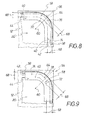
- FIG. 8 illustrates a corner region 56 of Isolierstoffköpers 12, wherein the trench 42 for the dam bead 44 on the one hand by the edge 40 of the maralt Vietnamese believing metal layer 20 and on the other hand by the metal layer frame is limited.
- the edge 40 in the respective corner region 56 is formed with a rounding 70 and also the inner edge 74 of the metal layer frame 38 in said corner region 56 with a rounding 76.
- the center of curvature of the rounding 70 and the rounding 76 is also in FIG. 8 with the reference numeral 60 - as in the FIGS. 5 and 6 - designated.
- FIG. 8 Same details are in FIG. 8 with the same reference numerals as in FIG. 6 referred, so that it is unnecessary, in connection with FIG. 8 to describe all the details again.
- FIG. 9 illustrates a formation of a corner region 56 of the insulating material 12 of the circuit arrangement, wherein the edge 40 of the structured metal layer 20 with a chamfer 72 - see also the FIG. 7 - Is formed, and wherein also the inner edge 74 of the insulating material body 12 encircling metal layer frame 38 is formed with a chamfer 72 compliant chamfering 78.
Landscapes
- Structures Or Materials For Encapsulating Or Coating Semiconductor Devices Or Solid State Devices (AREA)
- Casings For Electric Apparatus (AREA)
- Shielding Devices Or Components To Electric Or Magnetic Fields (AREA)
- Insulated Metal Substrates For Printed Circuits (AREA)
- Lead Frames For Integrated Circuits (AREA)
Abstract
Description
- Die Erfindung betrifft eine Schaltungsanordnung mit einem Isolierstoffkörper, der an einer Hauptfläche eine schaltstrukturierte Metallschicht und mindestens ein hierauf angebrachtes Leistungshalbleiterbauelement aufweist, und mit einer auf dem Isolierstoffkörper angebrachten, der Kontur des Isolierstoffkörpers mit dem hierauf angebrachten mindestens einen Leistungshalbleiterbauelement folgenden Lage einer Isolationsmasse.
- Eine derartige Schaltungsanordnung ist aus der
DE 10 2004 021 927 B4 bekannt. Bei der Isolationsmasse dieser bekannten Schaltungsanordnung handelt es sich um eine zähflüssige dielektrische Isolationsmasse, wobei nach dem Aufbringen der zähflüssigen dielektrischen Isolationsmasse eine Vernetzung derselben eingeleitet wird. Anschließend erfolgt eine Drehung des Isolierstoffkörpers um eine zu seiner Hochachse senkrechte Achse, so dass die zähflüssige dielektrische Isolationsmasse die von Bonddrahtverbindungen gebildeten schaltungsgerechten Verbindungen des mindestens einen Leistungshalbleiterbauelementes umschließt und überschüssige zähflüssige Isolationsmasse gravitationsbedingt vom Isolierstoffkörper abtropft. Der mit der Isolationsmasse-Lage versehene Isolierstoffkörper wird in einem Gehäuse angeordnet, wonach eine vollständige Vernetzung der dielektrischen Isolationsmasse erfolgt, wodurch sich zwischen dem Gehäuse und dem Isolierstoffkörper eine Klebeverbindung ergibt. - Bei dieser bekannten Schaltungsanordnung ist nicht zuverlässig zu vermeiden, dass die zähflüssige dielektrische Isolationsmasse insbesondere während der Drehung des Isolierstoffkörpers über dessen Rand abfließt. Außerdem kann es durch den sogenannten "Pumpeffekt" zwischen der Isolationsmasse-Lage und dem Gehäuse zu einem Loslösen der Isolationsmasse vom Isolierstoffkörper kommen, so dass die Isolationsabdeckung unterbrochen wird. Daraus resultieren IsolationsSchwachstellen, die im Extremfall zu einem Ausfall der Schaltungsanordnung führen können.
- Der Erfindung liegt die Aufgabe zugrunde, eine Schaltungsanordnung der eingangs genannten Art zu schaffen, wobei eine unerwünschte Unterbrechung der Isolationsabdeckung auf einfache Weise verhindert wird.
- Diese Aufgabe wird erfindungsgemäß durch die Merkmale des Anspruches 1, d.h. dadurch gelöst, dass entlang des Randbereiches der die schaltstrukturierte Metallschicht aufweisenden Hauptfläche des Isolierstoffkörpers ein vom Rand der schaltstrukturierten Metallschicht durch einen Graben beabstandeter Metallschichtrahmen umläuft, und dass ein Dammwulst aus einem Vergußmaterial oder einem dem Vergußmaterial ähnlichen Material mit höherer Viskosität den umlaufenden Graben teilweise oder bevorzugt vollständig ausfüllt, wobei der Dammwulst sich zwischen dem Metallschichtrahmen und dem Rand der schaltstrukturierten Metallschicht erstreckt und zur Begrenzung der Lage aus der Isolationsmasse vorgesehen ist.
- Durch den Graben, der einerseits durch den Rand der schaltstrukturierten Metallschicht und andererseits durch den umlaufenden Metallschichtrahmen begrenzt ist, wird dem Vergußmaterial für den Dammwulst ein definierter Raum auf dem Isolierstoffkörper geboten, d.h. eine sichere Positionierung des Dammwulst-Vergußmaterials gewährleistet, so dass das Vergußmaterial für den Dammwulst nicht über den umlaufenden Rand des Isolierstoffkörpers ungewollt abtropft. Die Isolationsmasse-Lage wird mittels des Dammwulstes definiert begrenzt und an einem Abtropfen über den Rand des Isolierstoffkörpers gehindert. Ein unerwünschtes Loslösen der Isolationsmasse-Lage wird erfindungsgemäß verhindert, so dass eine Unterbrechung der Isolationsabdeckung, die zu Isolationsschwachstellen und im Extremfall zu einem Ausfall der Schaltungsanordnung führen würde, auf einfache Weise vermieden wird.
- Die schaltstrukturierte Metallschicht und der Metallschichtrahmen bestehen vorzugsweise aus demselben Metall, bspw. aus Kupfer, oder aus derselben Metalllegierung. Der Isolierstoffkörper besteht bspw. aus einer Industriekeramik wie Al2O3 o.dgl.
- Der den Metallschichtrahmen vom Rand der benachbarten schaltstrukturierten Metallschicht beabstandende Graben erstreckt sich vorzugsweise bis zur zugehörigen Hauptfläche des Isolierstoffkörpers, er wird bspw. durch Ätzen der an der entsprechenden Hauptfläche des Isolierstoffkörpers vorgesehenen Metallschicht - gleichzeitig mit der Schaltstrukturierung derselben - realisiert.
- Damit der zwischen dem Metallschichtrahmen und dem Rand der schaltstrukturierten Metallschicht vorhanden Dammwulst weiter verbessert auf dem Isolierstoffkörper fixiert wird, kann es vorteilhaft sein, wenn der Metallschichtrahmen in seiner Längserstreckung mit voneinander beabstandeten Vertiefungen ausgebildet ist. Die Vertiefungen können wie der oben erwähnte Graben durch Ätzen - gleichzeitig mit der Herstellung des Grabens - hergestellt werden.
- Der Metallschichtrahmen kann sich bis zum umlaufenden Rand des Isolierstoffkörpers erstrecken oder vom Rand des Isolierstoffkörpers einen definierten Abstand aufweisen, um ein Gehäuse der Schaltungsanordnung mittels des Dammwulstes mit dem Isolierstoffkörper zu verkleben oder den umlaufenden Dammwulst vom Gehäuse der Schaltungsanordnung definiert zu beabstanden.
- Aus der
DE 10 2008 26 347 A1 ist zwar eine Schaltungsanordnung mit einem Isolierstoffkörper bekannt, der an einer Hauptfläche eine schaltstrukturierte Metallschicht aufweist, die gegenüber einem Grundkörper ein hohes elektrisches Potential besitzt, und deren Rand vom Rand des Isolierstoffkörpers beabstandet ist, wobei im Randbereich zwischen dem Rand der schaltstrukturierten Metallschicht und dem Rand des Isolierstoffkörpers voneinander beabstandete Metallschichtrahmen vorgesehen sind. Der randseitig äußerste Metallschichtrahmen ist mit dem Grundkörper elektrisch leitend verbunden, um die Durchschlagfestigkeit der Schaltungsanordnung am Randbereich des Isolierstoffkörpers unabhängig von der Art des Isolierstoffkörpers zu erhöhen. Dieser Gesichtspunkt hat mit der vorliegenden Erfindung jedoch keine Gemeinsamkeiten. - Der Dammwulst wird auf den Isolierstoffkörper üblicherweise mittels einer Düseneinrichtung aufgebracht. Im Bereich der jeweiligen Ecke des Isolierstoffkörpers wird die Düseneinrichtung aus produktionstechnischen Gründen, d.h. aus Produktivitäts-Gründen jedoch nicht angehalten, um eine Umstellung der Düseneinrichtung von der einen Raumrichtung in die dazu senkrechte Raumrichtung zu bewirken, sondern die Düseneinrichtung bewegt sich im jeweiligen Eckenbereich des Isolierstoffkörpers entlang einer abgerundeten Bahn mit einem kleinen Krümmungsradius. Ist der Rand der schaltstrukturierten Metallschicht der Schaltungsanordnung im Bereich der jeweiligen Ecke des Isolierstoffkörpers jedoch mit einer scharfkantig rechtwinkeligen Ecke ausgebildet, so resultiert aus dem dort abgerundeten Verlauf des Dammwulstes eine Reduktion des Isolationsabstandes zwischen der Ecke der schaltstrukturierten Metallschicht und dem Außenrand des Dammwulstes. Diese Reduktion des Isolationsabstandes kann sich auf die Isolationsfestigkeit nachteilig auswirken. Um das zu vermeiden, hat es sich als zweckmäßig erwiesen, wenn der Dammwulst im jeweiligen Eckenbereich des Isolierstoffkörpers abgerundet verläuft, und der Rand der schaltstrukturierten Metallschicht im jeweiligen Eckenbereich der schaltstrukturierten Metallschicht mit einer Abrundung oder mit einer Abfasung ausgebildet ist. Dabei ist es vorteilhaft, wenn die Abrundung oder die Abfasung des Randes der schaltstrukturierten Metallschicht an die im jeweiligen Eckenbereich des Isolierstoffkörpers ausgebildete Abrundung des Dammwulstes angepaßt ist.
- Besonders vorteilhaft ist es, wenn der Dammwulst im jeweiligen Eckenbereich des Isolierstoffkörpers abgerundet verläuft, und wenn der Metallschichtrahmen einen Innenrand aufweist, der im jeweiligen Eckenbereich des Isolierstoffkörpers mit einer Abrundung oder mit einer Abfasung ausgebildet ist. Bei einer solchen Ausbildung der zuletzt genannten Art ist es bevorzugt, wenn die Abrundung oder die Abfasung des Innenrandes des Metallschichtrahmens an die im jeweiligen Eckenbereich des Isolierstoffkörpers ausgebildete Abrundung des Dammwulstes angepaßt ist.
- Weitere Einzelheiten, Merkmale und Vorteile ergeben sich aus der nachfolgenden Beschreibung eines in der Zeichnung schematisch dargestellten Ausführungsbeispieles der erfindungsgemäßen Schaltungsanordnung.
- Es zeigen:
-
Figur 1 eine schematische Schnittdarstellung der Schaltungsanordnung in einem vergrößerten Maßstab, -
Figur 2 das Detail II gemäßFigur 1 in einem weiter vergrößerten Maßstab, -
Figur 3 das Detail III gemäßFigur 1 in einem derFigur 2 ähnlichen vergrößerten Maßstab, -
Figur 4 abschnittweise in einem vergrößerten Maßstab eine Darstellung des Metallschichtrahmens - zur Verdeutlichung von Vertiefungen - in einer Ansicht von oben, -
Figur 5 abschnittweise vergrößert einen Eckenbereich des Isolierstoffkörpers zur Verdeutlichung der Problematik eines in dem besagten Eckenbereich abgerundet verlaufenden Dammwulstes, -
Figur 6 eine derFigur 5 ähnliche schematische Darstellung eines Eckenbereiches des Isolierstoffkörpers mit dort abgerundet verlaufendem Dammwulst und einer Abrundung des Randes der schaltstrukturierten Metallschicht in diesem Eckenbereich, -
Figur 7 eine derFigur 6 ähnliche Darstellung mit einer Abfasung des Randes der schaltstrukturierten Metallschicht im Eckenbereich des Isolierstoffkörpers, -
Figur 8 eine derFigur 6 prinzipiell ähnliche Darstellung mit einem Metallschichtrahmen, dessen Innenrand im entsprechenden Eckenbereich des Isolierstoffkörpers mit einer Abrundung ausgebildet ist, und -
Figur 9 eine derFigur 7 prinzipiell ähnliche Darstellung zur Verdeutlichung eines Metallschichtrahmens, dessen Innenrand im jeweiligen Eckenbereich des Isolierstoffkörpers mit einer Abfasung ausgebildet ist. -
Figur 1 zeigt eine Ausbildung der Schaltungsanordnung 10 mit einem Isolierstoffkörper 12, der an einer Hauptfläche 14 eine Metallschicht 16 aufweist. Die Metallschicht 16 ist an der Hauptfläche 14 vollflächig vorgesehen. An der von der Hauptfläche 14 abgewandten Hauptfläche 18 des Isolierstoffkörpers 12 ist zur Ausbildung von Leiterbahnen eine schaltstrukturierte Metallschicht 20 vorgesehen. An der schaltstrukturierten Metallschicht 20 sind Leistungshalbleiterbauelemente 22 wie Dioden, Thyristoren, IGBTs und/oder MOS-FETs sowie Sensorbauelemente 24 vorgesehen. Die Leistungshalbleiterbauelemente 22 sind mit der schaltstrukturierten Metallschicht 20 mittels Drahtbondverbindungen 26 zusammengeschaltet. - Mit der Bezugsziffer 28 sind Kontaktfedern bezeichnet, die zur elektrischen Verbindung der Leiterbahnen bildenden schaltstrukturierten Metallschicht 20 mit (nicht gezeichneten) externen Zuleitungen dienen. Zu diesem Zwecke erstrecken sich die Kontaktfedern 28 geringfügig aus einem Gehäuse 30 der Schaltungsanordnung 10 heraus. Selbstverständlich sind die dargestellten Kontaktfedern nur eine mögliche Ausgestaltung derartiger Anschlusselementen.
- Auf dem Isolierstoffkörper 12 ist eine Lage 32 aus einer Isolationsmasse 33 angebracht, wobei die Oberflächen-Kontur 34 der Lage 32 den Leistungshalbleiterbauelementen 22 folgt und die Isolationsmasse 33 die Drahtbondverbindungen 26 umschließt.
- Wie auch aus den
Figuren 2 und 3 ersichtlich ist, läuft entlang des Randbereiches der die schaltstrukturierte Metallschicht 20 aufweisenden Hauptfläche 18 des Isolierstoffkörpers 12 ein Metallschichtrahmen 38 um. Der Metallschichtrahmen 38 ist vom Rand 40 der schaltstrukturierten Metallschicht 20 durch einen Graben 42 beabstandet, der zur definierten Positionierung eines Dammwulstes 44 vorgesehen ist. Der Dammwulst 44 besteht aus einem Vergußmaterial 46, er dient zur randseitigen Begrenzung der Isolationsmasse 33 der Lage 32, er erstreckt sich zwischen dem Metallschichtrahmen 38 und dem Rand 40 der schaltstrukturierten Metallschicht 20, d.h. vom Metallschichtrahmen 38 bis zur schaltstrukturierten Metallschicht 20. - Zur weiter verbesserten Fixierung des Vergußmaterials 46 des Dammwulstes 44 kann der Metallschichtrahmen 38 in seiner Längserstreckung mit voneinander beabstandeten Vertiefungen 48 (siehe
Figur 4 ) ausgebildet sein. - Die Leiterbahnen bildende, schaltstrukturierte Metallschicht 20 und der randseitig um den Isolierstoffkörper 12 umlaufende Metallschichtrahmen 38 bestehen vorzugsweise aus demselben Metall, bspw. aus Kupfer. Der umlaufende Graben 42 für den Dammwulst 44 kann durch Ätzen hergestellt werden, wobei sich der Graben 42 bis zur zugehörigen Hauptfläche 18 des Isolierstoffkörpers 12 erstreckt. Gleichzeitig mit der Herstellung des umlaufenden Grabens 42 können im Metallschichtrahmen 38 auch die Vertiefungen 48 z.B. durch Ätzen hergestellt werden.
-
Figur 2 verdeutlicht eine Ausbildungsvariante, wobei das Gehäuse 30 mittels des Vergußmaterials 46 des Dammwulstes 44 mit dem vom Isolierstoffkörper 12, der vollflächigen Metallschicht 16 und der schaltstrukturierten Metallschicht 20 gebildeten Substrat 50 fest verbunden ist. Demgegenüber verdeutlicht dieFigur 3 eine Ausbildung der Schaltungsanordnung 10, bei welcher das Gehäuse 30 vom Dammwulst 44 beabstandet ist und auf eine andere an sich bekannte Weise mit einem Grundkörper 52, bei dem es sich bspw. um einen Kühlkörper handelt, mechanisch fest verbunden sein kann. Bei der Ausbildung gemäßFigur 2 befindet sich der umlaufende Metallschichtrahmen 38 in unmittelbarer Nähe des umlaufenden Randes 54 des Isolierstoffkörpers 12 des Substrates 50. Demgegenüber verdeutlicht dieFigur 3 eine Ausbildung, bei welcher der Metallschichtrahmen 38 vom Rand 54 des Isolierstoffkörpers 12 definiert beabstandet ist, um den Dammwulst 44 vom Gehäuse 30 der Schaltungsanordnung zu beabstanden. - Gleiche Einzelheiten sind in den
Figuren 1 bis 4 jeweils mit denselben Bezugsziffern bezeichnet, so dass es sich erübrigt, in Verbindung mit diesen Figuren alle Einzelheiten jeweils detailliert zu beschreiben. -
Figur 5 verdeutlicht abschnittweise einen Eckenbereich 56 des Isolierstoffkörpers 12. Mit der Bezugsziffer 44 ist der Dammwulst bezeichnet, der im Eckenbereich 56 mit einer Abrundung 58 ausgebildet ist, um den Dammwulst mit Hilfe einer (nicht gezeichneten) Düseneinrichtung zeitsparend herstellen zu können. Die Abrundung 58 des Dammwulstes 44 weist einen Krümmungsmittelpunkt 60 auf. - Ist der Rand 40 der schaltstrukturierten Metallschicht 20 im Eckenbereich 56 des Isolierstoffkörpers 12 mit einer Ecke 62 ausgebildet, so ergibt sich zwischen dem Außenrand 64 des Dammwulstes 44 und der Ecken 62 der schaltstrukturierten Metallschicht 20 an der jeweiligen Abrundung 58 eine Reduktion des Isolierabstandes, die durch den Doppelpfeil 66 verdeutlicht ist. Entlang den zueinander senkrecht orientierten, geradlinig verlaufenden Abschnitten weist der Dammwulst 44 demgegenüber einen Isolationsabstand auf, der durch den Doppelpfeil 68 verdeutlicht ist.
- Um eine solche Reduktion des Isolationsabstandes im jeweiligen Eckenbereich 56 des Isolierstoffkörpers 12 zu vermeiden, kann der Rand 40 der schaltstrukturierten Metallschicht 20 im jeweiligen Eckenbereich 56 mit einer Abrundung 70, wie sie in
Figur 6 dargestellt ist, oder mit einer Abfasung 72, wie sie inFigur 7 gezeichnet ist, ausgebildet sein. - Gleiche Einzelheiten sind in den
Figuren 6 und 7 mit denselben Bezugsziffern wie inFigur 5 bezeichnet, so dass es sich erübrigt, in Verbindung mit denFiguren 6 und 7 alle Einzelheiten noch einmal detailliert zu beschreiben. -
Figur 8 verdeutlicht einen Eckenbereich 56 des Isolierstoffköpers 12, wobei der Graben 42 für den Dammwulst 44 einerseits durch den Rand 40 der schaltstrukturierten Metallschicht 20 und andererseits durch den Metallschichtrahmen begrenzt ist. Bei dieser Ausbildung der Schaltungsanordnung ist der Rand 40 im jeweiligen Eckenbereich 56 mit einer Abrundung 70 und außerdem der Innenrand 74 des Metallschichtrahmens 38 im besagten Eckenbereich 56 mit einer Abrundung 76 ausgebildet. Der Krümmungsmittelpunkt der Abrundung 70 und der Abrundung 76 ist auch inFigur 8 mit der Bezugsziffer 60 - wie in denFiguren 5 und 6 - bezeichnet. - Gleiche Einzelheiten sind in
Figur 8 mit denselben Bezugsziffern wie inFigur 6 bezeichnet, so dass es sich erübrigt, in Verbindung mitFigur 8 alle Einzelheiten noch einmal zu beschreiben. -
Figur 9 verdeutlicht eine Ausbildung eines Eckenbereiches 56 des Isolierstoffkörpers 12 der Schaltungsanordnung, wobei der Rand 40 der schaltstrukturierten Metallschicht 20 mit einer Abfasung 72 - siehe auch dieFigur 7 - ausgebildet ist, und wobei auch der Innenrand 74 des um den Isolierstoffkörper 12 umlaufenden Metallschichtrahmens 38 mit einer zur Abfasung 72 konformen Abfasung 78 ausgebildet ist. - Gleiche Einzelheiten sind in
Figur 9 mit denselben Bezugsziffern wie inFigur 7 bezeichnet, so dass es sich erübrigt, in Verbindung mitFigur 9 alle Einzelheiten noch einmal zu beschreiben. -
- 10
- Schaltungsanordnung
- 12
- Isolierstoffkörper (von 10)
- 14
- Hauptfläche (von 12)
- 16
- flächige Metallschicht (an 14)
- 18
- Hauptfläche (von 12)
- 20
- schaltstrukturierte Metallschicht (an 18)
- 22
- Leistungshalbleiterbauelement (an 20)
- 24
- Sensorbauelement (an 22)
- 26
- Drahtbondverbindung (zwischen 22 und 20)
- 28
- Kontaktfeder (von 10)
- 30
- Gehäuse (von 10)
- 32
- Isolationslage (auf 12)
- 33
- Isolationsmasse (von 32)
- 34
- Oberflächen-Kontur (von 32)
- 36
- Randbereich (von 18)
- 38
- Metallschichtrahmen (an 36)
- 40
- Rand (von 20)
- 42
- Graben (zwischen 40 und 38 für 44)
- 44
- Dammwulst (für 32)
- 46
- Vergußmaterial (von 44)
- 48
- Vertiefung (in 38 für 44)
- 50
- Substrat (aus 12, 16 und 20)
- 52
- Grundkörper (von 10)
- 54
- umlaufender Rand (von 12)
- 56
- Eckenbereich (von 12)
- 58
- Abrundung (von 44)
- 60
- Krümmungsmittelpunkt (von 58)
- 62
- Ecke (von 40)
- 64
- Außenrand (von 44)
- 66
- Reduktion des Isolationsabstandes (zwischen 62 und 64 bei 56)
- 68
- Isolationsabstand (zwischen 62 und 64)
- 70
- Abrundung (von 40 bei 56)
- 72
- Abfasung (von 40 bis 56)
- 74
- Innenrand (von 38)
- 76
- Abrundung (von 74 bei 56)
- 78
- Abfasung (von 74 bei 56)
Claims (9)
- Schaltungsanordnung, mit einem Isolierstoffkörper (12), der an einer Hauptfläche (18) eine schaltstrukturierte Metallschicht (20) und mindestens ein hierauf angebrachtes Leistungshalbleiterbauelement (22) aufweist, und mit einer auf dem Isolierstoffkörper (12) angebrachten, der Oberflächen-Kontur des Isolierstoffkörpers (12) mit dem hierauf angebrachten mindestens einen Leistungshalbleiterbauelement (22) folgenden Lage (32) einer Isolationsmasse (33),
dadurch gekennzeichnet,
dass entlang des Randbereiches (36) der die schaltstrukturierte Metallschicht (20) aufweisenden Hauptfläche (18) des Isolierstoffkörpers (12) ein vom Rand (40) der schaltstrukturierten Metallschicht (20) durch einen Graben (42) beabstandeter Metallschichtrahmen (38) umläuft, und dass ein Dammwulst (44) aus einem Vergußmaterial (46) den umlaufenden Graben (42) ausfüllt, wobei der Dammwulst (44) zur Begrenzung der Lage (32) aus der Isolationsmasse (33) vorgesehen ist und sich zwischen dem Metallschichtrahmen (38) und dem Rand (40) der schaltstrukturierten Metallschicht (20) erstreckt. - Schaltungsanordnung nach Anspruch 1,
dadurch gekennzeichnet,
dass die schaltstrukturierte Metallschicht (20) und der Metallschichtrahmen (38) aus demselben Metall oder derselben Metalllegierung bestehen. - Schaltungsanordnung nach Anspruch 1,
dadurch gekennzeichnet,
dass der den Metallschichtrahmen (38) vom Rand (40) der benachbarten schaltstrukturierten Metallschicht (20) beabstandende Graben (42) sich bis zur zugehörigen Hauptfläche (18) des Isolierstoffkörpers (12) erstreckt. - Schaltungsanordnung nach Anspruch 1,
dadurch gekennzeichnet,
dass der Metallschichtrahmen (38) in seiner Längserstreckung mit voneinander beabstandeten Vertiefungen (48) ausgebildet ist. - Schaltungsanordnung nach einem der Ansprüche 1 bis 4,
dadurch gekennzeichnet,
dass der Metallschichtrahmen (38) am umlaufenden Rand (54) des Isolierstoffkörpers (12) vorgesehen ist oder vom Rand (54) einen Abstand aufweist. - Schaltungsanordnung nach einem der Ansprüche 1 bis 5,
dadurch gekennzeichnet,
dass der Dammwulst (44) im jeweiligen Eckenbereich (56) des Isolierstoffkörpers (12) mit einer Abrundung (58) verläuft und der Rand (40) der schaltstrukturierten Metallschicht (20) im jeweiligen Eckenbereich (56) mit einer Abrundung (70) oder mit einer Abfasung (72) ausgebildet ist. - Schaltungsanordnung nach Anspruch 6,
dadurch gekennzeichnet,
dass die Abrundung (70) oder die Abfasung (72) des Randes (40) der schaltstrukturierten Metallschicht (20) an die im jeweiligen Eckenbereich (56) des Isolierstoffkörpers (12) ausgebildete Abrundung (58) des Dammwulstes (44) angepaßt ist. - Schaltungsanordnung nach einem der Ansprüche 1 bis 7,
dadurch gekennzeichnet,
dass der Dammwulst (44) im jeweiligen Eckenbereich (56) des Isolierstoffkörpers (12) mit einer Abrundung (58) verläuft und der Metallschichtrahmen (38) einen Innenrand (74) aufweist, der im jeweiligen Eckenbereich (56) mit einer Abrundung (76) oder mit einer Abfasung (78) ausgebildet ist. - Schaltungsanordnung nach Anspruch 8,
dadurch gekennzeichnet,
dass die Abrundung (76) oder die Abfasung (78) des Innenrandes (74) des Metallschichtrahmens (38) an die im jeweiligen Eckenbereich (56) des Isolierstoffkörpers (12) ausgebildete Abrundung (58) des Dammwulstes (44) angepaßt ist.
Applications Claiming Priority (1)
| Application Number | Priority Date | Filing Date | Title |
|---|---|---|---|
| DE102011004544A DE102011004544B4 (de) | 2011-02-22 | 2011-02-22 | Schaltungsanordnung |
Publications (3)
| Publication Number | Publication Date |
|---|---|
| EP2492957A2 true EP2492957A2 (de) | 2012-08-29 |
| EP2492957A3 EP2492957A3 (de) | 2012-11-07 |
| EP2492957B1 EP2492957B1 (de) | 2013-09-11 |
Family
ID=45445959
Family Applications (1)
| Application Number | Title | Priority Date | Filing Date |
|---|---|---|---|
| EP12150873.3A Active EP2492957B1 (de) | 2011-02-22 | 2012-01-12 | Schaltungsanordnung |
Country Status (4)
| Country | Link |
|---|---|
| EP (1) | EP2492957B1 (de) |
| KR (1) | KR101789835B1 (de) |
| CN (1) | CN102651347B (de) |
| DE (1) | DE102011004544B4 (de) |
Families Citing this family (1)
| Publication number | Priority date | Publication date | Assignee | Title |
|---|---|---|---|---|
| DE102020131493B4 (de) | 2020-11-27 | 2023-04-13 | Semikron Elektronik Gmbh & Co. Kg | Verkettete Anlage und Verfahren zur inneren elektrischen Isolation einer leistungselektronischen Schalteinrichtung |
Citations (2)
| Publication number | Priority date | Publication date | Assignee | Title |
|---|---|---|---|---|
| DE102004021927B4 (de) | 2004-05-04 | 2008-07-03 | Semikron Elektronik Gmbh & Co. Kg | Verfahren zur inneren elektrischen Isolation eines Substrats für ein Leistungshalbleitermodul |
| DE102008026347A1 (de) | 2008-05-31 | 2010-02-18 | Semikron Elektronik Gmbh & Co. Kg | Leistungselektronische Anordnung mit einem Substrat und einem Grundkörper |
Family Cites Families (6)
| Publication number | Priority date | Publication date | Assignee | Title |
|---|---|---|---|---|
| US4814943A (en) * | 1986-06-04 | 1989-03-21 | Oki Electric Industry Co., Ltd. | Printed circuit devices using thermoplastic resin cover plate |
| JPS6444051A (en) * | 1987-08-12 | 1989-02-16 | Hitachi Ltd | Semiconductor device |
| JP2005531137A (ja) * | 2002-04-29 | 2005-10-13 | アドヴァンスト インターコネクト テクノロジーズ リミテッド | 部分的にパターン形成したリードフレームならびに半導体パッケージングにおけるその製造および使用の方法 |
| US6800948B1 (en) * | 2002-07-19 | 2004-10-05 | Asat Ltd. | Ball grid array package |
| DE10337640A1 (de) * | 2003-08-16 | 2005-03-17 | Semikron Elektronik Gmbh | Leistungshalbleitermodul mit verbessertem thermischen Kontakt |
| DE102004021122B4 (de) | 2004-04-29 | 2007-10-11 | Semikron Elektronik Gmbh & Co. Kg | Anordnung in Druckkontaktierung mit einem Leistungshalbleitermodul |
-
2011
- 2011-02-22 DE DE102011004544A patent/DE102011004544B4/de active Active
-
2012
- 2012-01-12 EP EP12150873.3A patent/EP2492957B1/de active Active
- 2012-02-17 KR KR1020120016180A patent/KR101789835B1/ko active Active
- 2012-02-22 CN CN201210042235.8A patent/CN102651347B/zh active Active
Patent Citations (2)
| Publication number | Priority date | Publication date | Assignee | Title |
|---|---|---|---|---|
| DE102004021927B4 (de) | 2004-05-04 | 2008-07-03 | Semikron Elektronik Gmbh & Co. Kg | Verfahren zur inneren elektrischen Isolation eines Substrats für ein Leistungshalbleitermodul |
| DE102008026347A1 (de) | 2008-05-31 | 2010-02-18 | Semikron Elektronik Gmbh & Co. Kg | Leistungselektronische Anordnung mit einem Substrat und einem Grundkörper |
Also Published As
| Publication number | Publication date |
|---|---|
| DE102011004544A1 (de) | 2012-08-23 |
| EP2492957A3 (de) | 2012-11-07 |
| KR20120096424A (ko) | 2012-08-30 |
| CN102651347B (zh) | 2016-03-09 |
| KR101789835B1 (ko) | 2017-10-25 |
| DE102011004544B4 (de) | 2013-06-13 |
| CN102651347A (zh) | 2012-08-29 |
| EP2492957B1 (de) | 2013-09-11 |
Similar Documents
| Publication | Publication Date | Title |
|---|---|---|
| DE102011077543B4 (de) | Halbleitervorrichtung | |
| DE102007012154B4 (de) | Halbleitermodul mit Halbleiterchips und Verfahren zur Herstellung desselben | |
| DE112018002137B4 (de) | Halbleiterbauteil | |
| DE102011082781B4 (de) | Halbleitervorrichtung mit einer plattenelektrode zum verbinden einer mehrzahl an halbleiterchips | |
| EP2784809B1 (de) | Leistungshalbleitermodul und Verfahren zur Herstellung eines Leistungshalbleitermoduls | |
| DE102013226544B4 (de) | Halbleitervorrichtung | |
| DE102005049687B4 (de) | Leistungshalbleiterbauteil in Flachleitertechnik mit vertikalem Strompfad und Verfahren zur Herstellung | |
| DE112017007415T5 (de) | Halbleiterbauelement, Verfahren zur Herstellung desselben und Leistungswandlervorrichtung | |
| DE102015210603A1 (de) | Verfahren zur Herstellung einer Halbleitervorrichtung | |
| DE102009037257A1 (de) | Leistungshalbleitermodul mit Schaltungsträger und Lastanschlusselement sowie Herstellungsverfahren hierzu | |
| DE102014115815B4 (de) | Verfahren zur herstellung eines schaltungsträgers, verfahren zur herstellung einer halbleiteranordung, verfahren zum betrieb einer halbleiteranordnung und verfahren zur herstellung eines halbleitermoduls | |
| DE102018212438A1 (de) | Halbleitergehäuse mit elektromagnetischer abschirmstruktur und verfahren zu dessen herstellung | |
| DE102015115122A1 (de) | Leistungshalbleitermodul mit zweiteiligem Gehäuse | |
| DE112014003204B4 (de) | Leistungsmodul | |
| DE102013219959B4 (de) | Halbleitervorrichtung und Verfahren zum Herstellen derselben | |
| DE102020125705A1 (de) | Leistungs-Halbleitervorrichtung | |
| DE112016005807T5 (de) | Halbleitereinheit und Verfahren zur Herstellung derselben | |
| DE102013216035B3 (de) | Leistungshalbleitermodul und Verfahren zur Herstellung eines Leistungshalbleitermoduls | |
| DE102008058003B4 (de) | Verfahren zur Herstellung eines Halbleitermoduls und Halbleitermodul | |
| DE102015223300B4 (de) | Halbleitervorrichtung | |
| DE102005039165A1 (de) | Halbleiterleistungsbauteil mit vertikalem Strompfad durch einen Halbleiterleistungschip und Verfahren zu dessen Herstellung | |
| EP2492957B1 (de) | Schaltungsanordnung | |
| DE112022005438T5 (de) | Halbleiterbauteil und Verfahren zur Herstellung des Halbleiterbauteils | |
| DE102014115201B4 (de) | Verfahren zum verlöten eines schaltungsträgers mit einer trägerplatte | |
| EP1959494B1 (de) | Leistungshalbleitermodul |
Legal Events
| Date | Code | Title | Description |
|---|---|---|---|
| PUAI | Public reference made under article 153(3) epc to a published international application that has entered the european phase |
Free format text: ORIGINAL CODE: 0009012 |
|
| AK | Designated contracting states |
Kind code of ref document: A2 Designated state(s): AL AT BE BG CH CY CZ DE DK EE ES FI FR GB GR HR HU IE IS IT LI LT LU LV MC MK MT NL NO PL PT RO RS SE SI SK SM TR |
|
| AX | Request for extension of the european patent |
Extension state: BA ME |
|
| PUAL | Search report despatched |
Free format text: ORIGINAL CODE: 0009013 |
|
| AK | Designated contracting states |
Kind code of ref document: A3 Designated state(s): AL AT BE BG CH CY CZ DE DK EE ES FI FR GB GR HR HU IE IS IT LI LT LU LV MC MK MT NL NO PL PT RO RS SE SI SK SM TR |
|
| AX | Request for extension of the european patent |
Extension state: BA ME |
|
| RIC1 | Information provided on ipc code assigned before grant |
Ipc: H01L 23/24 20060101AFI20121001BHEP Ipc: H01L 25/07 20060101ALI20121001BHEP |
|
| 17P | Request for examination filed |
Effective date: 20121203 |
|
| GRAP | Despatch of communication of intention to grant a patent |
Free format text: ORIGINAL CODE: EPIDOSNIGR1 |
|
| INTG | Intention to grant announced |
Effective date: 20130617 |
|
| GRAS | Grant fee paid |
Free format text: ORIGINAL CODE: EPIDOSNIGR3 |
|
| GRAA | (expected) grant |
Free format text: ORIGINAL CODE: 0009210 |
|
| AK | Designated contracting states |
Kind code of ref document: B1 Designated state(s): AL AT BE BG CH CY CZ DE DK EE ES FI FR GB GR HR HU IE IS IT LI LT LU LV MC MK MT NL NO PL PT RO RS SE SI SK SM TR |
|
| REG | Reference to a national code |
Ref country code: GB Ref legal event code: FG4D Free format text: NOT ENGLISH |
|
| REG | Reference to a national code |
Ref country code: CH Ref legal event code: EP |
|
| REG | Reference to a national code |
Ref country code: AT Ref legal event code: REF Ref document number: 632045 Country of ref document: AT Kind code of ref document: T Effective date: 20130915 |
|
| REG | Reference to a national code |
Ref country code: IE Ref legal event code: FG4D Free format text: LANGUAGE OF EP DOCUMENT: GERMAN |
|
| REG | Reference to a national code |
Ref country code: CH Ref legal event code: NV Representative=s name: BRAUNPAT BRAUN EDER AG, CH |
|
| REG | Reference to a national code |
Ref country code: DE Ref legal event code: R096 Ref document number: 502012000102 Country of ref document: DE Effective date: 20131107 |
|
| PG25 | Lapsed in a contracting state [announced via postgrant information from national office to epo] |
Ref country code: SE Free format text: LAPSE BECAUSE OF FAILURE TO SUBMIT A TRANSLATION OF THE DESCRIPTION OR TO PAY THE FEE WITHIN THE PRESCRIBED TIME-LIMIT Effective date: 20130911 Ref country code: CY Free format text: LAPSE BECAUSE OF FAILURE TO SUBMIT A TRANSLATION OF THE DESCRIPTION OR TO PAY THE FEE WITHIN THE PRESCRIBED TIME-LIMIT Effective date: 20130911 Ref country code: LT Free format text: LAPSE BECAUSE OF FAILURE TO SUBMIT A TRANSLATION OF THE DESCRIPTION OR TO PAY THE FEE WITHIN THE PRESCRIBED TIME-LIMIT Effective date: 20130911 Ref country code: HR Free format text: LAPSE BECAUSE OF FAILURE TO SUBMIT A TRANSLATION OF THE DESCRIPTION OR TO PAY THE FEE WITHIN THE PRESCRIBED TIME-LIMIT Effective date: 20130911 Ref country code: NO Free format text: LAPSE BECAUSE OF FAILURE TO SUBMIT A TRANSLATION OF THE DESCRIPTION OR TO PAY THE FEE WITHIN THE PRESCRIBED TIME-LIMIT Effective date: 20131211 |
|
| REG | Reference to a national code |
Ref country code: NL Ref legal event code: VDEP Effective date: 20130911 |
|
| REG | Reference to a national code |
Ref country code: LT Ref legal event code: MG4D |
|
| PG25 | Lapsed in a contracting state [announced via postgrant information from national office to epo] |
Ref country code: FI Free format text: LAPSE BECAUSE OF FAILURE TO SUBMIT A TRANSLATION OF THE DESCRIPTION OR TO PAY THE FEE WITHIN THE PRESCRIBED TIME-LIMIT Effective date: 20130911 Ref country code: GR Free format text: LAPSE BECAUSE OF FAILURE TO SUBMIT A TRANSLATION OF THE DESCRIPTION OR TO PAY THE FEE WITHIN THE PRESCRIBED TIME-LIMIT Effective date: 20131212 Ref country code: SI Free format text: LAPSE BECAUSE OF FAILURE TO SUBMIT A TRANSLATION OF THE DESCRIPTION OR TO PAY THE FEE WITHIN THE PRESCRIBED TIME-LIMIT Effective date: 20130911 Ref country code: LV Free format text: LAPSE BECAUSE OF FAILURE TO SUBMIT A TRANSLATION OF THE DESCRIPTION OR TO PAY THE FEE WITHIN THE PRESCRIBED TIME-LIMIT Effective date: 20130911 |
|
| REG | Reference to a national code |
Ref country code: SK Ref legal event code: T3 Ref document number: E 15381 Country of ref document: SK |
|
| PG25 | Lapsed in a contracting state [announced via postgrant information from national office to epo] |
Ref country code: RO Free format text: LAPSE BECAUSE OF FAILURE TO SUBMIT A TRANSLATION OF THE DESCRIPTION OR TO PAY THE FEE WITHIN THE PRESCRIBED TIME-LIMIT Effective date: 20130911 Ref country code: IS Free format text: LAPSE BECAUSE OF FAILURE TO SUBMIT A TRANSLATION OF THE DESCRIPTION OR TO PAY THE FEE WITHIN THE PRESCRIBED TIME-LIMIT Effective date: 20140111 Ref country code: NL Free format text: LAPSE BECAUSE OF FAILURE TO SUBMIT A TRANSLATION OF THE DESCRIPTION OR TO PAY THE FEE WITHIN THE PRESCRIBED TIME-LIMIT Effective date: 20130911 Ref country code: CZ Free format text: LAPSE BECAUSE OF FAILURE TO SUBMIT A TRANSLATION OF THE DESCRIPTION OR TO PAY THE FEE WITHIN THE PRESCRIBED TIME-LIMIT Effective date: 20130911 Ref country code: EE Free format text: LAPSE BECAUSE OF FAILURE TO SUBMIT A TRANSLATION OF THE DESCRIPTION OR TO PAY THE FEE WITHIN THE PRESCRIBED TIME-LIMIT Effective date: 20130911 |
|
| PG25 | Lapsed in a contracting state [announced via postgrant information from national office to epo] |
Ref country code: ES Free format text: LAPSE BECAUSE OF FAILURE TO SUBMIT A TRANSLATION OF THE DESCRIPTION OR TO PAY THE FEE WITHIN THE PRESCRIBED TIME-LIMIT Effective date: 20130911 Ref country code: PL Free format text: LAPSE BECAUSE OF FAILURE TO SUBMIT A TRANSLATION OF THE DESCRIPTION OR TO PAY THE FEE WITHIN THE PRESCRIBED TIME-LIMIT Effective date: 20130911 |
|
| REG | Reference to a national code |
Ref country code: DE Ref legal event code: R097 Ref document number: 502012000102 Country of ref document: DE |
|
| PG25 | Lapsed in a contracting state [announced via postgrant information from national office to epo] |
Ref country code: PT Free format text: LAPSE BECAUSE OF FAILURE TO SUBMIT A TRANSLATION OF THE DESCRIPTION OR TO PAY THE FEE WITHIN THE PRESCRIBED TIME-LIMIT Effective date: 20140113 |
|
| PLBE | No opposition filed within time limit |
Free format text: ORIGINAL CODE: 0009261 |
|
| STAA | Information on the status of an ep patent application or granted ep patent |
Free format text: STATUS: NO OPPOSITION FILED WITHIN TIME LIMIT |
|
| BERE | Be: lapsed |
Owner name: SEMIKRON ELEKTRONIK G.M.B.H. & CO. KG Effective date: 20140131 |
|
| 26N | No opposition filed |
Effective date: 20140612 |
|
| PG25 | Lapsed in a contracting state [announced via postgrant information from national office to epo] |
Ref country code: LU Free format text: LAPSE BECAUSE OF FAILURE TO SUBMIT A TRANSLATION OF THE DESCRIPTION OR TO PAY THE FEE WITHIN THE PRESCRIBED TIME-LIMIT Effective date: 20140112 Ref country code: IT Free format text: LAPSE BECAUSE OF FAILURE TO SUBMIT A TRANSLATION OF THE DESCRIPTION OR TO PAY THE FEE WITHIN THE PRESCRIBED TIME-LIMIT Effective date: 20130911 |
|
| REG | Reference to a national code |
Ref country code: DE Ref legal event code: R097 Ref document number: 502012000102 Country of ref document: DE Effective date: 20140612 |
|
| REG | Reference to a national code |
Ref country code: HU Ref legal event code: AG4A Ref document number: E020317 Country of ref document: HU |
|
| PG25 | Lapsed in a contracting state [announced via postgrant information from national office to epo] |
Ref country code: DK Free format text: LAPSE BECAUSE OF FAILURE TO SUBMIT A TRANSLATION OF THE DESCRIPTION OR TO PAY THE FEE WITHIN THE PRESCRIBED TIME-LIMIT Effective date: 20130911 |
|
| REG | Reference to a national code |
Ref country code: IE Ref legal event code: MM4A |
|
| PG25 | Lapsed in a contracting state [announced via postgrant information from national office to epo] |
Ref country code: IE Free format text: LAPSE BECAUSE OF NON-PAYMENT OF DUE FEES Effective date: 20140112 |
|
| PG25 | Lapsed in a contracting state [announced via postgrant information from national office to epo] |
Ref country code: MC Free format text: LAPSE BECAUSE OF FAILURE TO SUBMIT A TRANSLATION OF THE DESCRIPTION OR TO PAY THE FEE WITHIN THE PRESCRIBED TIME-LIMIT Effective date: 20130911 |
|
| PG25 | Lapsed in a contracting state [announced via postgrant information from national office to epo] |
Ref country code: BE Free format text: LAPSE BECAUSE OF NON-PAYMENT OF DUE FEES Effective date: 20150131 |
|
| REG | Reference to a national code |
Ref country code: FR Ref legal event code: PLFP Year of fee payment: 5 |
|
| PG25 | Lapsed in a contracting state [announced via postgrant information from national office to epo] |
Ref country code: MT Free format text: LAPSE BECAUSE OF FAILURE TO SUBMIT A TRANSLATION OF THE DESCRIPTION OR TO PAY THE FEE WITHIN THE PRESCRIBED TIME-LIMIT Effective date: 20130911 |
|
| PG25 | Lapsed in a contracting state [announced via postgrant information from national office to epo] |
Ref country code: SM Free format text: LAPSE BECAUSE OF FAILURE TO SUBMIT A TRANSLATION OF THE DESCRIPTION OR TO PAY THE FEE WITHIN THE PRESCRIBED TIME-LIMIT Effective date: 20130911 |
|
| PG25 | Lapsed in a contracting state [announced via postgrant information from national office to epo] |
Ref country code: RS Free format text: LAPSE BECAUSE OF NON-PAYMENT OF DUE FEES Effective date: 20130911 Ref country code: BG Free format text: LAPSE BECAUSE OF FAILURE TO SUBMIT A TRANSLATION OF THE DESCRIPTION OR TO PAY THE FEE WITHIN THE PRESCRIBED TIME-LIMIT Effective date: 20130911 |
|
| PG25 | Lapsed in a contracting state [announced via postgrant information from national office to epo] |
Ref country code: TR Free format text: LAPSE BECAUSE OF FAILURE TO SUBMIT A TRANSLATION OF THE DESCRIPTION OR TO PAY THE FEE WITHIN THE PRESCRIBED TIME-LIMIT Effective date: 20130911 Ref country code: BE Free format text: LAPSE BECAUSE OF FAILURE TO SUBMIT A TRANSLATION OF THE DESCRIPTION OR TO PAY THE FEE WITHIN THE PRESCRIBED TIME-LIMIT Effective date: 20140131 |
|
| REG | Reference to a national code |
Ref country code: FR Ref legal event code: PLFP Year of fee payment: 6 |
|
| PGFP | Annual fee paid to national office [announced via postgrant information from national office to epo] |
Ref country code: HU Payment date: 20161229 Year of fee payment: 6 Ref country code: SK Payment date: 20170105 Year of fee payment: 6 |
|
| REG | Reference to a national code |
Ref country code: FR Ref legal event code: PLFP Year of fee payment: 7 |
|
| REG | Reference to a national code |
Ref country code: AT Ref legal event code: MM01 Ref document number: 632045 Country of ref document: AT Kind code of ref document: T Effective date: 20170112 |
|
| REG | Reference to a national code |
Ref country code: CH Ref legal event code: PCAR Free format text: NEW ADDRESS: HOLEESTRASSE 87, 4054 BASEL (CH) |
|
| PG25 | Lapsed in a contracting state [announced via postgrant information from national office to epo] |
Ref country code: AT Free format text: LAPSE BECAUSE OF NON-PAYMENT OF DUE FEES Effective date: 20170112 |
|
| PG25 | Lapsed in a contracting state [announced via postgrant information from national office to epo] |
Ref country code: MK Free format text: LAPSE BECAUSE OF FAILURE TO SUBMIT A TRANSLATION OF THE DESCRIPTION OR TO PAY THE FEE WITHIN THE PRESCRIBED TIME-LIMIT Effective date: 20130911 |
|
| REG | Reference to a national code |
Ref country code: SK Ref legal event code: MM4A Ref document number: E 15381 Country of ref document: SK Effective date: 20180112 |
|
| PG25 | Lapsed in a contracting state [announced via postgrant information from national office to epo] |
Ref country code: HU Free format text: LAPSE BECAUSE OF NON-PAYMENT OF DUE FEES Effective date: 20180113 Ref country code: AL Free format text: LAPSE BECAUSE OF FAILURE TO SUBMIT A TRANSLATION OF THE DESCRIPTION OR TO PAY THE FEE WITHIN THE PRESCRIBED TIME-LIMIT Effective date: 20130911 |
|
| PG25 | Lapsed in a contracting state [announced via postgrant information from national office to epo] |
Ref country code: SK Free format text: LAPSE BECAUSE OF NON-PAYMENT OF DUE FEES Effective date: 20180112 |
|
| PGFP | Annual fee paid to national office [announced via postgrant information from national office to epo] |
Ref country code: GB Payment date: 20241205 Year of fee payment: 14 |
|
| PGFP | Annual fee paid to national office [announced via postgrant information from national office to epo] |
Ref country code: FR Payment date: 20241209 Year of fee payment: 14 |
|
| PGFP | Annual fee paid to national office [announced via postgrant information from national office to epo] |
Ref country code: DE Payment date: 20241203 Year of fee payment: 14 |
|
| PGFP | Annual fee paid to national office [announced via postgrant information from national office to epo] |
Ref country code: CH Payment date: 20250201 Year of fee payment: 14 |
|
| REG | Reference to a national code |
Ref country code: DE Ref legal event code: R081 Ref document number: 502012000102 Country of ref document: DE Owner name: SEMIKRON DANFOSS ELEKTRONIK GMBH & CO. KG, DE Free format text: FORMER OWNER: SEMIKRON ELEKTRONIK GMBH & CO. KG, 90431 NUERNBERG, DE |
|
| REG | Reference to a national code |
Ref country code: DE Ref legal event code: R079 Ref document number: 502012000102 Country of ref document: DE Free format text: PREVIOUS MAIN CLASS: H01L0023240000 Ipc: H10W0076470000 |