EP2472698A2 - Système d'alimentation électrique embarqué et procédé de protection - Google Patents
Système d'alimentation électrique embarqué et procédé de protection Download PDFInfo
- Publication number
- EP2472698A2 EP2472698A2 EP11192468A EP11192468A EP2472698A2 EP 2472698 A2 EP2472698 A2 EP 2472698A2 EP 11192468 A EP11192468 A EP 11192468A EP 11192468 A EP11192468 A EP 11192468A EP 2472698 A2 EP2472698 A2 EP 2472698A2
- Authority
- EP
- European Patent Office
- Prior art keywords
- power supply
- voltage
- supply system
- board power
- terminal
- Prior art date
- Legal status (The legal status is an assumption and is not a legal conclusion. Google has not performed a legal analysis and makes no representation as to the accuracy of the status listed.)
- Withdrawn
Links
Images


Classifications
-
- H—ELECTRICITY
- H02—GENERATION; CONVERSION OR DISTRIBUTION OF ELECTRIC POWER
- H02J—CIRCUIT ARRANGEMENTS OR SYSTEMS FOR SUPPLYING OR DISTRIBUTING ELECTRIC POWER; SYSTEMS FOR STORING ELECTRIC ENERGY
- H02J7/00—Circuit arrangements for charging or depolarising batteries or for supplying loads from batteries
- H02J7/0029—Circuit arrangements for charging or depolarising batteries or for supplying loads from batteries with safety or protection devices or circuits
- H02J7/0034—Circuit arrangements for charging or depolarising batteries or for supplying loads from batteries with safety or protection devices or circuits using reverse polarity correcting or protecting circuits
-
- B—PERFORMING OPERATIONS; TRANSPORTING
- B60—VEHICLES IN GENERAL
- B60R—VEHICLES, VEHICLE FITTINGS, OR VEHICLE PARTS, NOT OTHERWISE PROVIDED FOR
- B60R16/00—Electric or fluid circuits specially adapted for vehicles and not otherwise provided for; Arrangement of elements of electric or fluid circuits specially adapted for vehicles and not otherwise provided for
- B60R16/02—Electric or fluid circuits specially adapted for vehicles and not otherwise provided for; Arrangement of elements of electric or fluid circuits specially adapted for vehicles and not otherwise provided for electric constitutive elements
- B60R16/03—Electric or fluid circuits specially adapted for vehicles and not otherwise provided for; Arrangement of elements of electric or fluid circuits specially adapted for vehicles and not otherwise provided for electric constitutive elements for supply of electrical power to vehicle subsystems or for
Definitions
- Embodiments of the present invention relate to an on-board power supply system, and in particular to the reverse polarity protection of an on-board power supply system.
- Automotive on-board power supply systems usually include a battery and a generator.
- a plurality of electrical loads may be coupled to the on-board power supply system. These loads can include a starter, electrical motors, and lights, as well as control and driver units for driving the individual loads.
- Most of the electrical loads connected to an on-board power supply system require a supply voltage with a given polarity and must not have the polarity of their supply voltage reversed.
- Each of these loads may include a reverse polarity protection circuit or element, like a diode. This, however, increases the costs of the overall system.
- a reverse polarity error may occur when the on-board system is connected to an external power source, like a battery charger or the battery of another car. Connecting the battery to an external source can be required for charging the battery or for jump-start purposes.
- terminals for connecting an external power source are located remote from the battery and are connected to the on-board systems through electrically connecting wires. These terminals are also known as jump-start terminals or assist start terminals.
- the problem underlying the present invention is to provide an on-board power supply system that is robust against reverse polarization and to provide a method for protecting an on-board power supply system in case of reverse polarization.
- a first aspect relates to an on-board power supply system.
- the system includes a first and a second power supply terminal configured to have at least one of a battery and a generator connected thereto, a first external terminal coupled to the first power supply terminal, and a second external terminal coupled to the second power supply terminal, and a protection unit connected between the first external terminal and the first power supply terminal.
- the protection unit includes a semiconductor switching unit having a load path and a control terminal, the load path connected between the first external terminal and the first power supply terminal, and a control circuit coupled to the control terminal of the semiconductor switching unit and configured to switch the switching unit on and off dependent on at least one electrical parameter in the on-board power supply system.
- a second aspect relates to a method for protecting an on-board power supply system.
- the power supply system includes a first and a second power supply terminal configured to have at least one of a battery and a generator connected thereto, and a first external terminal coupled to the first power supply terminal, and a second external terminal coupled to the second power supply terminal.
- the method includes connecting a protection unit with a semiconductor switching unit between the first external terminal and the first power supply terminal, and switching the switching unit on and off dependent on at least one electrical parameter in the on-board power supply system.
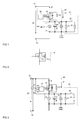
- FIG 1 schematically illustrates a first embodiment of an on-board power supply system, like an automotive on-board power supply system.
- the power supply system includes first and second power supply terminals 1, 2 configured to have at least one of a battery 11 and a generator 13 connected thereto.
- both a battery 11 and a generator 13 are connected to the power supply terminals 1, 2.
- the battery 11 can be a conventional automotive battery providing a supply voltage Vbat of 12V or, in modern cars, of 24V, 42V or 48V.
- the generator 13 can be a conventional generator driven by the internal combustion machine (not shown) and providing a supply voltage when driven by the internal combustion machine.
- the generator 13 can be a stand-alone generator or can be combined with a starter (starter-generator).
- a plurality of loads can be connected to the power supply terminals 1, 2.
- These loads include a starter 12 connected between the power supply terminals 1, 2 and a load arrangement 20 with a plurality of further electrical loads.
- These loads may include: electric window lifts; electric seat adjustments; a media device, like a radio, a CD or DVD player; internal and external lighting; a car navigation system; and safety devices, like ABS, airbags or seat-belt tensioners.
- the load arrangement 20 may include loads which are permanently connected to the power supply terminals 1, 2. These loads are commonly represented by load 21 illustrated in Figure 1 .
- the load arrangement 20 may further include loads which are only connected to the power supply terminals 1, 2 when the ignition key of the car has been turned on, which means when the ignition lock has been activated. In Figure 1 , these loads are represented by load 23.
- the ignition lock is represented by a switching element 22 connected between the load 23 and the power supply terminals 1, 2.
- the on-board power supply system further includes first and second external terminals 31, 32, wherein a first external terminal 31 is coupled to the first power supply terminal 1, and a second external terminal 32 is coupled to the second power supply terminal 2.
- Power supply terminals 1, 2 are, for example, formed by battery terminals (posts) of the battery 11. In modern cars the battery can be mounted at a location which is not or which is only difficult to access, like, for example, under the rear seat.
- the external terminals 31, 32 are located remote from the battery and are connected to the power supply terminals 1, 2 or the battery terminals, respectively, through electrically connecting lines. These external terminals 31, 32 allow to connect an external power source to the on-board power supply system or allow to connect an external electrical load to the on-board power supply system.
- An external power supply to be connected to the external terminals 31, 32 is, for example, a battery charger for charging the car battery 11 or is, for example, a battery of another car.
- the battery of another car is, for example, connected to the on-board power supply system when the car's own battery 11 is empty so that jump start or assist start is required.
- An external load connected to the externals 31, 32 can be the on-board power supply system of another car to which jump start is to be provided, or can be one of a plurality of different loads that can be powered by automotive on-board power supply systems, like a winch, a compressor, a lamp, etc.
- a generator like generator 13 of Figure 1 , usually includes an internal rectifier arrangement (not shown) which is capable of blocking a supply voltage between the power supply terminals 1, 2 with a first polarity, but which would allow a current to flow when a supply voltage with a second polarity - a reverse polarity relative to the first polarity - would be applied between the power supply terminals 1, 2.
- an internal rectifier arrangement (not shown) which is capable of blocking a supply voltage between the power supply terminals 1, 2 with a first polarity, but which would allow a current to flow when a supply voltage with a second polarity - a reverse polarity relative to the first polarity - would be applied between the power supply terminals 1, 2.
- the on-board power supply system of Figure 1 includes a reverse polarity protection unit 40 connected between the first external terminal 31 and the first power supply terminal 1. It should be noted, that the protection unit 40 could also be connected between the second power supply terminal 2 and the second external terminal 32, or that two protection units could be provided: a first one between the first external terminal 31 and the first power supply terminal 1, and a second one between the second power supply terminal 2 and the second external terminal 32.
- the protection unit 40 includes a semiconductor switching unit 41 having a load path and a control terminal, wherein the load path of the semiconductor switching unit 41 is connected between the first external terminal 31 and the first power supply terminal 1.
- the protection unit 40 further includes a control circuit 42 coupled to the control terminal of the semiconductor switching unit 41.
- the control circuit is configured to switch the semiconductor switching unit 41 on and off dependent on at least one electrical parameter of the on-board power supply system. This will be explained in further detail hereinbelow.
- the semiconductor switching unit 41 can be implemented with at least one transistor.
- this transistor is implemented as an n-type MOSFET having its source terminal connected to the first external terminal 31 and having its drain terminal connected to the first power supply terminal 1.
- implementing the semiconductor switching unit 41 with an n-type MOSFET is only an example. Any other type of semiconductor switching element, like a p-type MOSFET, an IGBT (Insulated Gate Bipolar Transistor), or a BJT (Bipolar Junction Transistor) can be used as well.
- a p-type MOSFET in the semiconductor switching unit 41 would have its drain terminal connected to the first external terminal 31, and would have its source terminal connected to the first power supply terminal 1.
- the semiconductor switching unit 41 can be implemented with one transistor. However, referring to Figure 2 , it is also possible to implement the semiconductor switching unit 41 with a plurality of two or more transistors 41 1 , 41 n having their load paths connected in parallel. In Figure 2 , these transistors are implemented as n-type transistors. However, any other type of transistor can be used as well.
- the semiconductor switching unit 41 can be switched on and off by the control circuit 42 via a control or drive signal S41.
- the semiconductor switching unit 41 When the semiconductor switching unit 41 is switched on, the power supply terminals 1, 2 of the on-board power supply system are electrically connected to the external terminals 31, 32.
- a current I3 can be supplied to the on-board power supply system via the external terminals 31, 32, or a current can be supplied by the on-board power supply system to the external terminals 31, 32.
- the current 13 flows in the direction as illustrated in Figure 1
- the current flows in the opposite direction.
- the control circuit 42 is configured to switch the semiconductor switching unit 41 off when an external voltage V3 is supplied between the external terminals 31, 32 which has a reverse polarity compared with the required polarity of the supply voltage of the on-board power supply system.
- the supply voltage of the on-board power supply system is the voltage Vbat provided by the battery and/or the generator.
- the first power supply terminal 1 of the on-board power supply system is a positive supply terminal, while the second supply terminal 2 is a negative supply terminal or reference terminal.
- the second power supply terminal 2 is connected to ground of the automobile in which the on-board power supply system is implemented.
- the external voltage V3 has a reverse polarity when the external voltage V3 is a negative voltage between the first and second external terminals 31, 32.
- the control circuit 42 is configured to evaluate at least one electrical parameter in the on-board power supply system in order to detect a reverse polarity of an external voltage V3, wherein the semiconductor switching unit 41 is switched off in order to protect the on-board power supply system when a reverse polarity is detected.
- control circuit 42 is configured to only evaluate a first voltage V3 which is the external voltage between the first and second external terminals 31, 32, and to switch the semiconductor switching unit off when this voltage is a negative voltage.
- the control circuit 42 is configured to evaluate a first voltage V3 which is the external voltage between the first and second external terminals 31, 32, and to evaluate a second voltage V4 which is the voltage between the first external terminal 31 and the first power supply terminal 1.
- the second voltage V4 corresponds to the voltage across the load path of the semiconductor switching unit 41.
- the protection unit 40 includes a first voltage measurement unit 44 configured to measure the first voltage V3 and to provide a first voltage measurement signal S3 to the control circuit 42.
- the first voltage measurement signal S3 is representative of the first voltage V3.
- the first voltage measurement signal S3 is proportional to the first voltage V3.
- the protection unit 40 further includes a second voltage measurement unit 45 which is configured to measure the second voltage V4 and to provide a second voltage measurement signal S4 to the control circuit 42.
- the second voltage measurement signal S4 is representative of the second voltage V4. According to one embodiment, the second voltage measurement signal S4 is proportional to the second voltage V4.
- the first and second voltage measurement units 44, 45 can be implemented as conventional voltage measurement units. Such voltage measurement units are commonly known, so that no further explanations are required in this regard.
- the control circuit 42 is configured to switch the semiconductor switching unit 41 on when the first voltage V3 is higher than a first threshold value V3 TH and when the second voltage V4 is outside a given first voltage range which ranges from a first voltage value V4 TH1 to a second voltage value V4 TH2 .
- the first threshold value V3 TH is, for example, below zero.
- the first threshold value V3 TH is selected from a voltage range ranging from about -5 V to about -0.05 V, in particular ranging from about -2 V to about -0.5 V.
- the external voltage V3 may approach zero value when a low-ohmic external load, such as a lamp, is connected to the external terminals 31, 32 and when the protection unit 40 is switched off. When the protection unit 40 then switches on, the load will be supplied by the battery 11.
- the first voltage value V4 TH1 is, for example, selected from a voltage of between about -5 V and about -0.05 V
- the second voltage value V4 TH2 which together with the first voltage value defines the first voltage range, is, for example, selected from a voltage of between about 0.05 V and about 1 V.
- the first voltage range is symmetrically relative to zero (0V), but the first voltage range could also be asymmetrical.
- FIG. 5 An embodiment of a control circuit 42 having a functionality as illustrated in Figure 4 , is schematically illustrated in Figure 5 .
- This control circuit 42 includes three comparators: a first comparator 421 for comparing the first voltage measurement signal S3 with a first threshold signal S3 TH representing the first threshold value V3 TH ; a second comparator 422 for comparing the second voltage measurement signal S4 with a first signal value S4 TH1 representing the first voltage value V4 TH1 ; and a third comparator 423 for comparing the second voltage measurement signal S4 with a second signal value S4 TH2 representing the second voltage value V4 TH2 .
- the drive signal S41 is available at an output of a first logic gate 425, which is an AND-gate in this case.
- the output signal S41 of the logic gate 425 is amplified using an amplifier or driver stage 426 in order to provide the drive signal for the semiconductor switching unit 41.
- the drive signal S41 may assume one of two different signal levels: an on-level at which the semiconductor switching unit 41 is switched on; and an off-level at which the semiconductor switching unit 41 is switched off. For explanation purposes it may be assumed that in the control circuit 42 in Figure 5 an on-level is a high signal level and that an off-level is a low signal level.
- the drive signal S41 assumes an on-level, when a comparator signal S421 of the first comparator 421 and when one of the comparator signals S422, S423 of the second and third comparators 422, 423 have an on-level.
- the first voltage V3 is above the threshold value V3 TH
- the second voltage V4 is outside the voltage range defined by the first and second voltage values V4 TH1 , V4 TH2 .
- the AND-gate 425 receives the first comparator signal S421 at a first input terminal.
- the second and third comparator signals S422, S423 are OR-connected by an OR-gate 424 wherein an output signal of the OR-gate 424 is received at a second input terminal of the AND-gate 425.
- control circuit 42 illustrated in Figure 5 represents only one of a plurality of different ways in which a control circuit having a functionality as illustrated in Figure 4 can be implemented.
- To evaluate the first and second voltages V3, V4 in order to decide whether or not the semiconductor switching unit 41 is switched on has the following effects: the on-board power supply system is protected from having an external voltage V3 with a reverse polarity connected thereto, because the semiconductor switching unit 41 is switched off when the external voltage V3 is below the threshold voltage V3 TH ; the switching unit 41 is also switched off when the voltage between the external terminals 31, 32 is only slightly different from the internal supply voltage Vbat between the power supply terminals 1, 2.
- the second voltage V4 would be within the first voltage range defined by the first and second voltage values V4 TH1 , V4 TH2 -
- the first and second external terminals are floating, which means that there is no external device connected to the external terminals.
- Figure 6 illustrates a first operating scenario in which an external voltage source 50 is connected between the first and second external terminals 31, 32.
- the external voltage source has the correct polarity, so that the voltage V3 between the external terminals 31, 32 is a positive voltage.
- the external voltage source 50 can be a battery charger, or can be a battery of another car.
- the protection unit 40 turns on, i.e., switches the semiconductor switching unit 41 (see Figures 1 and 3 ) on, when the external voltage V3 exceeds the internal power supply voltage Vbat for more than the second voltage value V4 TH2 .
- FIG. 7 illustrates a further operating scenario in which an external voltage source 50 is connected to the external terminals 31, 32.
- the external voltage source 50 is connected to the external terminals 31, 32 with a reverse polarity, so that the external voltage V3 equals the negative value -V50 of the supply voltage V50 provided by the external source 50.
- the absolute value of the supply voltage V50 of the external source 50 is higher than the absolute value of the first threshold value V3 TH , so that in this scenario the protection unit 40 is off, i.e., has its semiconductor switching unit 41 switched off.
- FIG 8 illustrates an operating scenario in which an external load 60 is connected to the external terminals 31, 32.
- the load 60 is represented as an impedance in Figure 8 .
- the load could also include a voltage source.
- the load 60 is, for example, an on-board power supply system of another car to which jump start is to be provided, but could also be any other kind of load which could be connected to the on-board power supply system of a car.
- the electrical potential of the first external terminal 31 is either drawn to ground GND or to the electrical potential of an internal voltage source (not shown) in the load 60. This causes a negative second voltage V4 across the protection unit 40, while the first voltage V3 is zero or positive.
- the protection unit 40 turns on when the absolute value of the voltage drop V4 across the protection unit 40 is higher than the first voltage value V4 TH1 .
- the protection unit 40 does not only protect the on-board power supply system from having a supply voltage with a reverse polarity connected thereto, but also allows to provide jump start to another car or to supply some external load connected to the external terminals 31, 32.
- the semiconductor switching unit 41 of the protection unit 40 is configured to have a high current-carrying capacity in order to protect the semiconductor switching unit 41 from being damaged when a short-circuit in the external load 60 (see Figure 8 ) occurs.
- the current-carrying capacity is, for example, selected such that it allows to discharge the car's own battery 11 without damaging or destroying the protection unit 40.
- the current-carrying capacity of the semiconductor switching unit 41 is 1000 A for 10 seconds or 500 A for 1 minute.
- the semiconductor switching unit 41 (see Figures 1 and 3 ) is implemented with at least one n-type MOSFET or at least one p-type MOSFET there is a diode present between the first external terminal 31 and the first power supply terminal 1, with the anode of the diode coupled to the first external terminal 31 and the cathode of the diode coupled to the first power supply terminal 1.
- This diode is the internal body diode of a MOSFET, in particular a power MOSFET. This body diode is also illustrated in the protection unit 40 of Figures 1 and 3 .
- the body diode conducts when an external voltage V3 is applied between the first and second external terminals 31, 32, and when this external voltage V3 is higher than the internal voltage Vbat for more than the forward voltage of the body diode.
- this body diode it would not be necessary to switch the semiconductor switching unit 41 on when an external voltage source is correctly connected to the external terminals 31, 32, like in the operating scenario illustrated in Figure 6 .
- electric losses that occur in a MOSFET which is in its on-state are lower than losses which occur in the forward-biased body diode, so that it is advantageous in terms of reducing power losses to switch the semiconductor switching unit on also when a positive supply voltage is supplied to the external terminals 31, 32.
- the semiconductor switching unit 41 is implemented with two MOSFETs 41 1 , 41 2 connected in series.
- these MOSFETs are n-type MOSFETs which have their drain terminals connected together.
- p-type MOSFETs instead of n-type MOSFETs could be used.
- the arrangement with the two MOSFETs 41 1 , 41 2 can block positive and negative voltages across the protection unit 40.
- the two MOSFETs 41 1 , 41 2 are switched on and off by the control circuit (not shown in Figure 9 ) simultaneously.
- a common control or drive signal S41 may be provided to the two MOSFETs 41 1 , 41 2 .
- separate drive signals are generated by the control circuit 42 and provided to the individual MOSFETs 41 1 , 41 2 .
- Figure 10 schematically illustrates a further embodiment of the control circuit 42.
- the control circuit 42 includes a logic unit 46 and a drive unit 47.
- logic unit 46 generates the drive signal S41 - which is amplified by the driver stage 47 - dependent on the first and second voltage measurement signals S3, S4.
- the logic unit 46 may include a logic circuit which corresponds to the logic circuit illustrated in Figure 5 .
- the driver stage 47 can be activated and deactivated by the logic unit 46.
- the logic unit 46 is configured to deactivate the driver stage 47 when or after the drive signal S41 assumes an off-level, and activates the driver stage 47 when or before the drive signal S41 assumes an on-level.
- the semiconductor switching unit 41 includes at least one transistor which is a normally-off transistor, so that the switched off semiconductor switching unit 41 remains in its off-state when the driver stage 47 is deactivated. By deactivating the driver stage 47, the power consumption of the protection unit 40 can be reduced. A low power consumption is in particular relevant when the car is parked and the battery is not charged.
- the logic unit 46 is not only configured to activate or deactivate the driver stage 47 dependent on the first and second voltage measurement signals S3, S4, but also dependent on an ignition signal S22.
- the ignition signal S22 represents a switching state of the ignition lock which is represented by switch 22 in the figures explained hereinbefore.
- the operating principle of the control circuit 42 of Figure 10 will be explained with reference to Figure 11 in which a state diagram is illustrated.
- the state diagram illustrates different operating states the protection unit 40 can assume.
- a first state 101 the protection unit 40 is turned off, which means that the semiconductor switching unit 41 is switched off and that the driver stage is deactivated.
- the protection unit 40 enters a second state 102 when the first and second voltage measurement signals S3, S4 indicate that the first voltage V3 is higher than the threshold value V3 TH and that the second voltage V4 is outside the voltage range defined by the first and second voltage values V4 TH1 , V4 TH2 .
- the ignition signal S22 is evaluated.
- the protection unit 40 When the ignition signal S22 indicates that the ignition lock has been activated (the ignition key has been turned on) the protection unit 40 is turned on in a third state 103.
- the sequence 101-102-103-101 of states is a typical sequence which may occur when jump start is received by the car, jump start is provided to another car or when an external load is supplied when the car is in operation, i.e., when the ignition key has been turned on.
- the protection unit 40 When it is determined in step 102 that the ignition lock is deactivated then the protection unit 40 is activated in state 104.
- the protection unit 40 leaves the on-state 104 to the off-state 101 when either the first voltage V3 falls below the threshold value V3 TH or when an internal timer which is activated when the protection unit 40 is turned on in state 104 has elapsed.
- the timer is, for example, set to a time period of several minutes up to several hours.
- the sequence 101-102-104-101 is a typical sequence when the on-board power supply system is connected to an external voltage source, like a battery charger, or to an external load, when the car is not in operation.
- the timer prevents that the protection unit is kept in its on-state - in which it consumes power - for a very long time during car parking.
- the protection unit 40 is turned off (transitions from state 104 to state 101) dependent on battery parameters.
- the protection unit 40 is, for example, switched off when a state of charge (SOC) of the battery falls below a given threshold, such as 50% of its capacity. This prevents the battery 11 from being unduly discharged by an external load. In this case, the protection unit 40 can only be switched on again for further supplying the load, when this is be confirmed by a user, for example, by turning on the ignition key. Thus, the transition from state 101 to 104 has to be locked until ignition key is turned to ON.
- SOC state of charge
- the protection unit 40 is switched off, when the state of charge (SOC) of the battery exceeds a given threshold, such as 90% of its capacity, and/or when a charging current falls below a given value, such as 10mA, for a given time, such as some minutes up to several hours, or even days. In this case, the protection unit 40 is switched off when the battery is sufficiently charged.
- SOC state of charge
- Figure 12 illustrates an embodiment in which two on-board power supply systems, namely the on-board power supply system explained herein before and a further on-board power supply system had their external terminals connected together.
- like features of the second on-board power supply system have the same reference characters as the first on-board power supply system, wherein the features of the second on-board power supply system have a reference character with index "1".
- an optional resistor 43 can be connected in parallel with the load path of the semiconductor switching unit 41 in the protection unit 40.
- This resistor 43 may help to set the potential at the first external terminal to a defined value. This is, in particular, useful when two on-board power supply systems with protection units are connected together.
- the resistor 43 is implemented as PTC (positive thermal coefficient) resistor.
- a switching element such as a transistor, or a transistor in series with a resistor, could be connected in parallel with the load path of the switching unit 41.
- resistor 43 another resistor (not shown) can be connected between the first external terminal 31 and ground.
- a diode 44 can be connected in parallel with the power supply terminals 1, 12. This diode 44 may clamp reverse voltage spikes.
- the semiconductor switching unit 41 and the control circuit 42 can be implemented in a common semiconductor chip or can be implemented in different semiconductor chips.
- control circuit is configured to prevent the semiconductor switching unit 41 from being switched on when an external load (60 in Figure 8 ) is connected to the external terminals. This may protect the car battery. According to one embodiment supplying an external load is prevented when the charging state of the battery 11 is low. In this case, the protection unit 40 also receives an information on the charging state of the battery from a sensor unit in order to evaluate this information.
- a supply voltage of the protection unit 40 in particular of the control circuit 42 of the protection unit 40, can be provided by the car battery 11 and/or by the voltage available at the external terminals 31, 32. If both of these voltages are voltages with a reverse polarity, the protection unit 40 would not be supplied, causing the protection unit 40 to be (stay) switched off.
- the semiconductor switching unit includes a normally-off transistor which is switched off when the protection unit 40 is not supplied with a suitable supply voltage.
- the external voltage (first voltage) V3 and the voltage (second voltage) V4 across the protection unit 40 are evaluated in order to decide whether or not the protection unit is to be activated (switched on) or deactivated (switched off).
- the current 13 through the protection unit 40 is evaluated instead of the second voltage.
- the protection unit 40 is activated when this current 13 is outside a given current range and when the first voltage is higher than the first threshold value V3 TH (see Figure 4 ).
- Figure 3 the dependency of the activation of the protection unit 40 on the current 13 is also schematically illustrated.
- the protection unit is deactivated or switched off, when the first voltage is below the threshold and/or when the current 13 is within a given range which includes zero.
- This current range ranges from a first threshold current I3 TH1 to a second threshold current I3 TH2 .
- the first threshold current I3 TH1 is, for example, between about -1A and about -100 ⁇ A, in particular ranging from about -1 00mA to about -1 mA
- the second threshold current I3 TH2 is, for example, between about 100 ⁇ A and about 1A, in particular ranging from about 1 mA to about 100mA.
- This current range can be symmetrically or asymmetrically relative to zero.
Landscapes
- Engineering & Computer Science (AREA)
- Power Engineering (AREA)
- Mechanical Engineering (AREA)
- Charge And Discharge Circuits For Batteries Or The Like (AREA)
- Emergency Protection Circuit Devices (AREA)
Applications Claiming Priority (1)
| Application Number | Priority Date | Filing Date | Title |
|---|---|---|---|
| US12/982,613 US9041244B2 (en) | 2010-12-30 | 2010-12-30 | On-board power supply protection |
Publications (2)
| Publication Number | Publication Date |
|---|---|
| EP2472698A2 true EP2472698A2 (fr) | 2012-07-04 |
| EP2472698A3 EP2472698A3 (fr) | 2017-07-12 |
Family
ID=45558463
Family Applications (1)
| Application Number | Title | Priority Date | Filing Date |
|---|---|---|---|
| EP11192468.4A Withdrawn EP2472698A3 (fr) | 2010-12-30 | 2011-12-07 | Système d'alimentation électrique embarqué et procédé de protection |
Country Status (3)
| Country | Link |
|---|---|
| US (1) | US9041244B2 (fr) |
| EP (1) | EP2472698A3 (fr) |
| CN (1) | CN102545199B (fr) |
Cited By (15)
| Publication number | Priority date | Publication date | Assignee | Title |
|---|---|---|---|---|
| DE102011056072B3 (de) * | 2011-12-06 | 2012-10-18 | Lear Corporation Gmbh | Schaltungsanordnung für einen Audio-Verstärker und System |
| DE102014114997A1 (de) * | 2014-07-03 | 2016-01-07 | The Noco Company | Tragbare Starthilfevorrichtung für Fahrzeugbatterien mit Sicherheitsschutzvorrichtung |
| US9770992B2 (en) | 2014-07-03 | 2017-09-26 | The Noco Company | Portable vehicle battery jump start apparatus with safety protection and jumper cable device therefor |
| FR3054736A1 (fr) * | 2016-07-29 | 2018-02-02 | Continental Automotive France | Unite de commande electronique et procede de gestion de l'alimentation d'une telle unite de commande electronique |
| USD867985S1 (en) | 2017-12-21 | 2019-11-26 | The Noco Company | Combination jump starter and display |
| US11458851B2 (en) | 2014-07-03 | 2022-10-04 | The Noco Company | Jump starting apparatus |
| US11611222B2 (en) | 2017-12-14 | 2023-03-21 | The Noco Company | Portable vehicle battery jump starter with air pump |
| USD984381S1 (en) | 2020-11-25 | 2023-04-25 | The Noco Company | Battery cable assembly for jump starting device |
| USD988999S1 (en) | 2018-10-03 | 2023-06-13 | The Noco Company | Battery clamp |
| USD991177S1 (en) | 2018-10-01 | 2023-07-04 | The Noco Company | Battery clamp |
| USD991186S1 (en) | 2020-12-11 | 2023-07-04 | The Noco Company | Battery cable assembly |
| USD991185S1 (en) | 2020-12-11 | 2023-07-04 | The Noco Company | Battery cable assembly |
| USD997102S1 (en) | 2018-10-03 | 2023-08-29 | The Noco Company | Battery clamp |
| USD1004550S1 (en) | 2018-10-03 | 2023-11-14 | The Noco Company | Battery clamp |
| USRE49976E1 (en) | 2016-06-30 | 2024-05-21 | Shenzhen Carku Technology Co., Ltd. | Battery clamp |
Families Citing this family (7)
| Publication number | Priority date | Publication date | Assignee | Title |
|---|---|---|---|---|
| US9245888B2 (en) * | 2012-09-29 | 2016-01-26 | Infineon Technologies Ag | Reverse polarity protection for n-substrate high-side switches |
| US9472948B2 (en) * | 2013-09-30 | 2016-10-18 | Infineon Technologies Ag | On chip reverse polarity protection compliant with ISO and ESD requirements |
| JP5734472B1 (ja) * | 2014-01-29 | 2015-06-17 | 三菱電機株式会社 | 車載電子制御装置 |
| US9484339B2 (en) | 2014-11-26 | 2016-11-01 | Infineon Technologies Ag | Smart semiconductor switch |
| US20170203666A1 (en) * | 2016-01-19 | 2017-07-20 | Ford Global Technologies, Llc | Battery charging system and servicing method |
| EP3750219A1 (fr) * | 2018-02-05 | 2020-12-16 | Pierburg Pump Technology GmbH | Unité auxiliaire automotrice dotée d'une unité de protection électronique |
| US11695283B2 (en) * | 2018-05-11 | 2023-07-04 | Texas Instruments Incorporated | Shoot-through current limiting circuit |
Family Cites Families (16)
| Publication number | Priority date | Publication date | Assignee | Title |
|---|---|---|---|---|
| US5539610A (en) * | 1993-05-26 | 1996-07-23 | Siliconix Incorporated | Floating drive technique for reverse battery protection |
| US5789900A (en) * | 1994-12-05 | 1998-08-04 | Fuji Photo Film Co., Ltd. | Device for protecting a secondary battery from overcharge and overdischarge |
| DE19719919A1 (de) * | 1997-05-13 | 1998-11-26 | Daimler Benz Ag | Anordnung zum Schutz von elektrischen Einrichtungen |
| DE19946744A1 (de) * | 1999-09-29 | 2001-05-10 | Tyco Electronics Logistics Ag | Verfahren zur sicheren Ankopplung eines Fremdspannungsnetzes an ein Betriebsspannungsnetz und Schaltungsanordnung zur Durchführung des Verfahrens |
| CA2363246C (fr) * | 2000-11-06 | 2006-02-21 | Research In Motion Limited | Chargeur de batteries portatif |
| US6803743B2 (en) * | 2002-10-04 | 2004-10-12 | Delphi Technologies, Inc. | Jump start and reverse battery protection circuit |
| DE10344896A1 (de) * | 2003-09-26 | 2005-04-21 | Bosch Gmbh Robert | Vorrichtung zur Absicherung eines Fremdenergieversorgungsanschlusses eines Fahrzeugs |
| JP4761454B2 (ja) * | 2006-02-23 | 2011-08-31 | セイコーインスツル株式会社 | 充放電保護回路および電源装置 |
| JP5400266B2 (ja) * | 2006-04-17 | 2014-01-29 | パナソニック株式会社 | 電界効果トランジスタ |
| JPWO2008108330A1 (ja) * | 2007-03-05 | 2010-06-17 | ボッシュ株式会社 | グロープラグ駆動装置 |
| US7692908B2 (en) * | 2008-01-02 | 2010-04-06 | Glj, Llc | Protection of polarity-sensitive components connected in parallel with a direct current motor or inductor |
| US7986055B2 (en) * | 2008-01-22 | 2011-07-26 | Honda Motor Co., Ltd. | Adjustment of control strategy based on temperature |
| WO2010052947A1 (fr) * | 2008-11-04 | 2010-05-14 | 株式会社村田製作所 | Unite d'alimentation de vehicule |
| CN201312124Y (zh) | 2008-12-09 | 2009-09-16 | 黄敬党 | 防止蓄电池充电反接的保护电路 |
| JP5439000B2 (ja) * | 2009-03-19 | 2014-03-12 | 株式会社東芝 | 組電池システム及び組電池の保護装置 |
| CN101888109B (zh) * | 2010-07-20 | 2012-12-05 | 衡阳中微科技开发有限公司 | 采用双向反接保护的蓄电池充电控制电路 |
-
2010
- 2010-12-30 US US12/982,613 patent/US9041244B2/en active Active
-
2011
- 2011-12-07 EP EP11192468.4A patent/EP2472698A3/fr not_active Withdrawn
- 2011-12-30 CN CN201110453501.1A patent/CN102545199B/zh active Active
Non-Patent Citations (1)
| Title |
|---|
| None |
Cited By (24)
| Publication number | Priority date | Publication date | Assignee | Title |
|---|---|---|---|---|
| DE102011056072B3 (de) * | 2011-12-06 | 2012-10-18 | Lear Corporation Gmbh | Schaltungsanordnung für einen Audio-Verstärker und System |
| US11447023B2 (en) | 2014-07-03 | 2022-09-20 | The Noco Company | Portable vehicle battery jump start apparatus with safety protection and jumper cable device thereof |
| US11667203B2 (en) | 2014-07-03 | 2023-06-06 | The Noco Company | Portable vehicle battery jump start apparatus with safety protection |
| US10328808B2 (en) | 2014-07-03 | 2019-06-25 | The Noco Company | Portable vehicle battery jump start apparatus with safety protection and jumper cable device thereof |
| US11766945B2 (en) | 2014-07-03 | 2023-09-26 | The Noco Company | Jump starting apparatus |
| US10604024B2 (en) | 2014-07-03 | 2020-03-31 | The Noco Company | Portable vehicle battery jump start apparatus with safety protection |
| US9770992B2 (en) | 2014-07-03 | 2017-09-26 | The Noco Company | Portable vehicle battery jump start apparatus with safety protection and jumper cable device therefor |
| US11458851B2 (en) | 2014-07-03 | 2022-10-04 | The Noco Company | Jump starting apparatus |
| DE102014114997B4 (de) * | 2014-07-03 | 2020-10-15 | The Noco Company | Tragbare Starthilfevorrichtung für Fahrzeugbatterien mit Sicherheitsschutzvorrichtung |
| US11584243B2 (en) | 2014-07-03 | 2023-02-21 | The Noco Company | Jump starting device with USB |
| DE102014114997A1 (de) * | 2014-07-03 | 2016-01-07 | The Noco Company | Tragbare Starthilfevorrichtung für Fahrzeugbatterien mit Sicherheitsschutzvorrichtung |
| USRE49976E1 (en) | 2016-06-30 | 2024-05-21 | Shenzhen Carku Technology Co., Ltd. | Battery clamp |
| FR3054736A1 (fr) * | 2016-07-29 | 2018-02-02 | Continental Automotive France | Unite de commande electronique et procede de gestion de l'alimentation d'une telle unite de commande electronique |
| US11611222B2 (en) | 2017-12-14 | 2023-03-21 | The Noco Company | Portable vehicle battery jump starter with air pump |
| USD867985S1 (en) | 2017-12-21 | 2019-11-26 | The Noco Company | Combination jump starter and display |
| USD991177S1 (en) | 2018-10-01 | 2023-07-04 | The Noco Company | Battery clamp |
| USD993920S1 (en) | 2018-10-03 | 2023-08-01 | The Noco Company | Battery clamp |
| USD997102S1 (en) | 2018-10-03 | 2023-08-29 | The Noco Company | Battery clamp |
| USD988999S1 (en) | 2018-10-03 | 2023-06-13 | The Noco Company | Battery clamp |
| USD1003833S1 (en) | 2018-10-03 | 2023-11-07 | The Noco Company | Battery clamp |
| USD1004550S1 (en) | 2018-10-03 | 2023-11-14 | The Noco Company | Battery clamp |
| USD984381S1 (en) | 2020-11-25 | 2023-04-25 | The Noco Company | Battery cable assembly for jump starting device |
| USD991185S1 (en) | 2020-12-11 | 2023-07-04 | The Noco Company | Battery cable assembly |
| USD991186S1 (en) | 2020-12-11 | 2023-07-04 | The Noco Company | Battery cable assembly |
Also Published As
| Publication number | Publication date |
|---|---|
| CN102545199B (zh) | 2016-01-27 |
| CN102545199A (zh) | 2012-07-04 |
| US9041244B2 (en) | 2015-05-26 |
| EP2472698A3 (fr) | 2017-07-12 |
| US20120169116A1 (en) | 2012-07-05 |
Similar Documents
| Publication | Publication Date | Title |
|---|---|---|
| US9041244B2 (en) | On-board power supply protection | |
| US8067859B2 (en) | Reverse polarity protection for MOSFETs | |
| US20050110467A1 (en) | Automotive jump starter with polarity detection and current routing circuitry | |
| JP6607927B2 (ja) | 高側ゲートドライバのための電力供給電圧の制御 | |
| US5539610A (en) | Floating drive technique for reverse battery protection | |
| JP6478789B2 (ja) | 半導体装置、電力制御用半導体装置、車載用電子制御ユニット及びそれを備えた車両 | |
| US8917039B2 (en) | Car power source apparatus and vehicle equipped with the power source apparatus | |
| US20110115287A1 (en) | Vehicular power supply circuit | |
| US9350238B2 (en) | Power supply device for vehicle including a boosting converter circuit | |
| JP2007082374A (ja) | 電源逆接続保護回路 | |
| US7288856B2 (en) | Reverse battery protection circuit for power switch | |
| JP2000253570A (ja) | 電気自動車のモータ起電力制御システム | |
| US11329474B2 (en) | Switching controller with adaptive overheating protection | |
| EP1601078A1 (fr) | Régulateur de tension MOS de puissance pour batteries | |
| US10164628B2 (en) | Switch box | |
| US20160094025A1 (en) | Current drivers that utilize short circuit protection | |
| CN113711284A (zh) | 用于车辆的传感器组件 | |
| US9407192B2 (en) | Method and apparatus for charging a bootstrap charge storage device | |
| JP2012222885A (ja) | 保護回路 | |
| US7477493B2 (en) | Alternator control device for vehicle | |
| EP0341460B1 (fr) | Circuit de protection pour actionneur | |
| JP2014024535A (ja) | 車両用電源装置 | |
| JP3457126B2 (ja) | 車両用交流発電機の制御装置 | |
| JP4155075B2 (ja) | 断線検出回路 | |
| US7130169B2 (en) | Short circuit protection for a power isolation device and associated diode |
Legal Events
| Date | Code | Title | Description |
|---|---|---|---|
| AK | Designated contracting states |
Kind code of ref document: A2 Designated state(s): AL AT BE BG CH CY CZ DE DK EE ES FI FR GB GR HR HU IE IS IT LI LT LU LV MC MK MT NL NO PL PT RO RS SE SI SK SM TR |
|
| AX | Request for extension of the european patent |
Extension state: BA ME |
|
| PUAI | Public reference made under article 153(3) epc to a published international application that has entered the european phase |
Free format text: ORIGINAL CODE: 0009012 |
|
| PUAL | Search report despatched |
Free format text: ORIGINAL CODE: 0009013 |
|
| AK | Designated contracting states |
Kind code of ref document: A3 Designated state(s): AL AT BE BG CH CY CZ DE DK EE ES FI FR GB GR HR HU IE IS IT LI LT LU LV MC MK MT NL NO PL PT RO RS SE SI SK SM TR |
|
| AX | Request for extension of the european patent |
Extension state: BA ME |
|
| RIC1 | Information provided on ipc code assigned before grant |
Ipc: H02J 7/00 20060101AFI20170608BHEP Ipc: B60R 16/03 20060101ALI20170608BHEP |
|
| 17P | Request for examination filed |
Effective date: 20180112 |
|
| RBV | Designated contracting states (corrected) |
Designated state(s): AL AT BE BG CH CY CZ DE DK EE ES FI FR GB GR HR HU IE IS IT LI LT LU LV MC MK MT NL NO PL PT RO RS SE SI SK SM TR |
|
| 17Q | First examination report despatched |
Effective date: 20190325 |
|
| STAA | Information on the status of an ep patent application or granted ep patent |
Free format text: STATUS: THE APPLICATION IS DEEMED TO BE WITHDRAWN |
|
| 18D | Application deemed to be withdrawn |
Effective date: 20200603 |