EP2469641A1 - Dye-sensitized solar cell and method for manufacturing the same - Google Patents
Dye-sensitized solar cell and method for manufacturing the same Download PDFInfo
- Publication number
- EP2469641A1 EP2469641A1 EP09848496A EP09848496A EP2469641A1 EP 2469641 A1 EP2469641 A1 EP 2469641A1 EP 09848496 A EP09848496 A EP 09848496A EP 09848496 A EP09848496 A EP 09848496A EP 2469641 A1 EP2469641 A1 EP 2469641A1
- Authority
- EP
- European Patent Office
- Prior art keywords
- dye
- stainless steel
- solar cell
- sensitized solar
- photoelectrode
- Prior art date
- Legal status (The legal status is an assumption and is not a legal conclusion. Google has not performed a legal analysis and makes no representation as to the accuracy of the status listed.)
- Granted
Links
Images
Classifications
-
- H—ELECTRICITY
- H10—SEMICONDUCTOR DEVICES; ELECTRIC SOLID-STATE DEVICES NOT OTHERWISE PROVIDED FOR
- H10F—INORGANIC SEMICONDUCTOR DEVICES SENSITIVE TO INFRARED RADIATION, LIGHT, ELECTROMAGNETIC RADIATION OF SHORTER WAVELENGTH OR CORPUSCULAR RADIATION
- H10F10/00—Individual photovoltaic cells, e.g. solar cells
-
- H—ELECTRICITY
- H01—ELECTRIC ELEMENTS
- H01G—CAPACITORS; CAPACITORS, RECTIFIERS, DETECTORS, SWITCHING DEVICES, LIGHT-SENSITIVE OR TEMPERATURE-SENSITIVE DEVICES OF THE ELECTROLYTIC TYPE
- H01G9/00—Electrolytic capacitors, rectifiers, detectors, switching devices, light-sensitive or temperature-sensitive devices; Processes of their manufacture
- H01G9/20—Light-sensitive devices
- H01G9/2095—Light-sensitive devices comprising a flexible sustrate
-
- C—CHEMISTRY; METALLURGY
- C21—METALLURGY OF IRON
- C21D—MODIFYING THE PHYSICAL STRUCTURE OF FERROUS METALS; GENERAL DEVICES FOR HEAT TREATMENT OF FERROUS OR NON-FERROUS METALS OR ALLOYS; MAKING METAL MALLEABLE, e.g. BY DECARBURISATION OR TEMPERING
- C21D6/00—Heat treatment of ferrous alloys
- C21D6/002—Heat treatment of ferrous alloys containing Cr
-
- C—CHEMISTRY; METALLURGY
- C21—METALLURGY OF IRON
- C21D—MODIFYING THE PHYSICAL STRUCTURE OF FERROUS METALS; GENERAL DEVICES FOR HEAT TREATMENT OF FERROUS OR NON-FERROUS METALS OR ALLOYS; MAKING METAL MALLEABLE, e.g. BY DECARBURISATION OR TEMPERING
- C21D6/00—Heat treatment of ferrous alloys
- C21D6/004—Heat treatment of ferrous alloys containing Cr and Ni
-
- C—CHEMISTRY; METALLURGY
- C22—METALLURGY; FERROUS OR NON-FERROUS ALLOYS; TREATMENT OF ALLOYS OR NON-FERROUS METALS
- C22C—ALLOYS
- C22C38/00—Ferrous alloys, e.g. steel alloys
- C22C38/002—Ferrous alloys, e.g. steel alloys containing In, Mg, or other elements not provided for in one single group C22C38/001 - C22C38/60
-
- C—CHEMISTRY; METALLURGY
- C22—METALLURGY; FERROUS OR NON-FERROUS ALLOYS; TREATMENT OF ALLOYS OR NON-FERROUS METALS
- C22C—ALLOYS
- C22C38/00—Ferrous alloys, e.g. steel alloys
- C22C38/004—Very low carbon steels, i.e. having a carbon content of less than 0,01%
-
- C—CHEMISTRY; METALLURGY
- C22—METALLURGY; FERROUS OR NON-FERROUS ALLOYS; TREATMENT OF ALLOYS OR NON-FERROUS METALS
- C22C—ALLOYS
- C22C38/00—Ferrous alloys, e.g. steel alloys
- C22C38/02—Ferrous alloys, e.g. steel alloys containing silicon
-
- C—CHEMISTRY; METALLURGY
- C22—METALLURGY; FERROUS OR NON-FERROUS ALLOYS; TREATMENT OF ALLOYS OR NON-FERROUS METALS
- C22C—ALLOYS
- C22C38/00—Ferrous alloys, e.g. steel alloys
- C22C38/04—Ferrous alloys, e.g. steel alloys containing manganese
-
- C—CHEMISTRY; METALLURGY
- C22—METALLURGY; FERROUS OR NON-FERROUS ALLOYS; TREATMENT OF ALLOYS OR NON-FERROUS METALS
- C22C—ALLOYS
- C22C38/00—Ferrous alloys, e.g. steel alloys
- C22C38/06—Ferrous alloys, e.g. steel alloys containing aluminium
-
- C—CHEMISTRY; METALLURGY
- C22—METALLURGY; FERROUS OR NON-FERROUS ALLOYS; TREATMENT OF ALLOYS OR NON-FERROUS METALS
- C22C—ALLOYS
- C22C38/00—Ferrous alloys, e.g. steel alloys
- C22C38/18—Ferrous alloys, e.g. steel alloys containing chromium
- C22C38/40—Ferrous alloys, e.g. steel alloys containing chromium with nickel
- C22C38/42—Ferrous alloys, e.g. steel alloys containing chromium with nickel with copper
-
- C—CHEMISTRY; METALLURGY
- C22—METALLURGY; FERROUS OR NON-FERROUS ALLOYS; TREATMENT OF ALLOYS OR NON-FERROUS METALS
- C22C—ALLOYS
- C22C38/00—Ferrous alloys, e.g. steel alloys
- C22C38/18—Ferrous alloys, e.g. steel alloys containing chromium
- C22C38/40—Ferrous alloys, e.g. steel alloys containing chromium with nickel
- C22C38/44—Ferrous alloys, e.g. steel alloys containing chromium with nickel with molybdenum or tungsten
-
- C—CHEMISTRY; METALLURGY
- C22—METALLURGY; FERROUS OR NON-FERROUS ALLOYS; TREATMENT OF ALLOYS OR NON-FERROUS METALS
- C22C—ALLOYS
- C22C38/00—Ferrous alloys, e.g. steel alloys
- C22C38/18—Ferrous alloys, e.g. steel alloys containing chromium
- C22C38/40—Ferrous alloys, e.g. steel alloys containing chromium with nickel
- C22C38/50—Ferrous alloys, e.g. steel alloys containing chromium with nickel with titanium or zirconium
-
- C—CHEMISTRY; METALLURGY
- C22—METALLURGY; FERROUS OR NON-FERROUS ALLOYS; TREATMENT OF ALLOYS OR NON-FERROUS METALS
- C22C—ALLOYS
- C22C38/00—Ferrous alloys, e.g. steel alloys
- C22C38/18—Ferrous alloys, e.g. steel alloys containing chromium
- C22C38/40—Ferrous alloys, e.g. steel alloys containing chromium with nickel
- C22C38/58—Ferrous alloys, e.g. steel alloys containing chromium with nickel with more than 1.5% by weight of manganese
-
- C—CHEMISTRY; METALLURGY
- C23—COATING METALLIC MATERIAL; COATING MATERIAL WITH METALLIC MATERIAL; CHEMICAL SURFACE TREATMENT; DIFFUSION TREATMENT OF METALLIC MATERIAL; COATING BY VACUUM EVAPORATION, BY SPUTTERING, BY ION IMPLANTATION OR BY CHEMICAL VAPOUR DEPOSITION, IN GENERAL; INHIBITING CORROSION OF METALLIC MATERIAL OR INCRUSTATION IN GENERAL
- C23F—NON-MECHANICAL REMOVAL OF METALLIC MATERIAL FROM SURFACE; INHIBITING CORROSION OF METALLIC MATERIAL OR INCRUSTATION IN GENERAL; MULTI-STEP PROCESSES FOR SURFACE TREATMENT OF METALLIC MATERIAL INVOLVING AT LEAST ONE PROCESS PROVIDED FOR IN CLASS C23 AND AT LEAST ONE PROCESS COVERED BY SUBCLASS C21D OR C22F OR CLASS C25
- C23F1/00—Etching metallic material by chemical means
- C23F1/10—Etching compositions
- C23F1/14—Aqueous compositions
- C23F1/16—Acidic compositions
- C23F1/28—Acidic compositions for etching iron group metals
-
- C—CHEMISTRY; METALLURGY
- C25—ELECTROLYTIC OR ELECTROPHORETIC PROCESSES; APPARATUS THEREFOR
- C25F—PROCESSES FOR THE ELECTROLYTIC REMOVAL OF MATERIALS FROM OBJECTS; APPARATUS THEREFOR
- C25F3/00—Electrolytic etching or polishing
- C25F3/02—Etching
- C25F3/06—Etching of iron or steel
-
- H—ELECTRICITY
- H01—ELECTRIC ELEMENTS
- H01M—PROCESSES OR MEANS, e.g. BATTERIES, FOR THE DIRECT CONVERSION OF CHEMICAL ENERGY INTO ELECTRICAL ENERGY
- H01M14/00—Electrochemical current or voltage generators not provided for in groups H01M6/00 - H01M12/00; Manufacture thereof
- H01M14/005—Photoelectrochemical storage cells
-
- H—ELECTRICITY
- H10—SEMICONDUCTOR DEVICES; ELECTRIC SOLID-STATE DEVICES NOT OTHERWISE PROVIDED FOR
- H10F—INORGANIC SEMICONDUCTOR DEVICES SENSITIVE TO INFRARED RADIATION, LIGHT, ELECTROMAGNETIC RADIATION OF SHORTER WAVELENGTH OR CORPUSCULAR RADIATION
- H10F71/00—Manufacture or treatment of devices covered by this subclass
-
- H—ELECTRICITY
- H10—SEMICONDUCTOR DEVICES; ELECTRIC SOLID-STATE DEVICES NOT OTHERWISE PROVIDED FOR
- H10F—INORGANIC SEMICONDUCTOR DEVICES SENSITIVE TO INFRARED RADIATION, LIGHT, ELECTROMAGNETIC RADIATION OF SHORTER WAVELENGTH OR CORPUSCULAR RADIATION
- H10F77/00—Constructional details of devices covered by this subclass
- H10F77/20—Electrodes
-
- C—CHEMISTRY; METALLURGY
- C21—METALLURGY OF IRON
- C21D—MODIFYING THE PHYSICAL STRUCTURE OF FERROUS METALS; GENERAL DEVICES FOR HEAT TREATMENT OF FERROUS OR NON-FERROUS METALS OR ALLOYS; MAKING METAL MALLEABLE, e.g. BY DECARBURISATION OR TEMPERING
- C21D8/00—Modifying the physical properties of ferrous metals or ferrous alloys by deformation combined with, or followed by, heat treatment
- C21D8/02—Modifying the physical properties of ferrous metals or ferrous alloys by deformation combined with, or followed by, heat treatment during manufacturing of plates or strips
- C21D8/04—Modifying the physical properties of ferrous metals or ferrous alloys by deformation combined with, or followed by, heat treatment during manufacturing of plates or strips to produce plates or strips for drawing, e.g. for deep-drawing
- C21D8/0421—Modifying the physical properties of ferrous metals or ferrous alloys by deformation combined with, or followed by, heat treatment during manufacturing of plates or strips to produce plates or strips for drawing, e.g. for deep-drawing characterised by the working steps
- C21D8/0436—Cold rolling
-
- H—ELECTRICITY
- H01—ELECTRIC ELEMENTS
- H01G—CAPACITORS; CAPACITORS, RECTIFIERS, DETECTORS, SWITCHING DEVICES, LIGHT-SENSITIVE OR TEMPERATURE-SENSITIVE DEVICES OF THE ELECTROLYTIC TYPE
- H01G9/00—Electrolytic capacitors, rectifiers, detectors, switching devices, light-sensitive or temperature-sensitive devices; Processes of their manufacture
- H01G9/20—Light-sensitive devices
- H01G9/2027—Light-sensitive devices comprising an oxide semiconductor electrode
- H01G9/2031—Light-sensitive devices comprising an oxide semiconductor electrode comprising titanium oxide, e.g. TiO2
-
- H—ELECTRICITY
- H01—ELECTRIC ELEMENTS
- H01G—CAPACITORS; CAPACITORS, RECTIFIERS, DETECTORS, SWITCHING DEVICES, LIGHT-SENSITIVE OR TEMPERATURE-SENSITIVE DEVICES OF THE ELECTROLYTIC TYPE
- H01G9/00—Electrolytic capacitors, rectifiers, detectors, switching devices, light-sensitive or temperature-sensitive devices; Processes of their manufacture
- H01G9/20—Light-sensitive devices
- H01G9/2059—Light-sensitive devices comprising an organic dye as the active light absorbing material, e.g. adsorbed on an electrode or dissolved in solution
-
- Y—GENERAL TAGGING OF NEW TECHNOLOGICAL DEVELOPMENTS; GENERAL TAGGING OF CROSS-SECTIONAL TECHNOLOGIES SPANNING OVER SEVERAL SECTIONS OF THE IPC; TECHNICAL SUBJECTS COVERED BY FORMER USPC CROSS-REFERENCE ART COLLECTIONS [XRACs] AND DIGESTS
- Y02—TECHNOLOGIES OR APPLICATIONS FOR MITIGATION OR ADAPTATION AGAINST CLIMATE CHANGE
- Y02E—REDUCTION OF GREENHOUSE GAS [GHG] EMISSIONS, RELATED TO ENERGY GENERATION, TRANSMISSION OR DISTRIBUTION
- Y02E10/00—Energy generation through renewable energy sources
- Y02E10/50—Photovoltaic [PV] energy
- Y02E10/542—Dye sensitized solar cells
-
- Y—GENERAL TAGGING OF NEW TECHNOLOGICAL DEVELOPMENTS; GENERAL TAGGING OF CROSS-SECTIONAL TECHNOLOGIES SPANNING OVER SEVERAL SECTIONS OF THE IPC; TECHNICAL SUBJECTS COVERED BY FORMER USPC CROSS-REFERENCE ART COLLECTIONS [XRACs] AND DIGESTS
- Y02—TECHNOLOGIES OR APPLICATIONS FOR MITIGATION OR ADAPTATION AGAINST CLIMATE CHANGE
- Y02P—CLIMATE CHANGE MITIGATION TECHNOLOGIES IN THE PRODUCTION OR PROCESSING OF GOODS
- Y02P70/00—Climate change mitigation technologies in the production process for final industrial or consumer products
- Y02P70/50—Manufacturing or production processes characterised by the final manufactured product
Definitions
- the present invention relates to a dye-sensitized solar cell in which stainless steel is used as the constitutive material of the photoelectrode (negative electrode), and to its production method.
- the mainstream of solar cells is toward those in which silicon is used as the photoelectric conversion element; however, as more economical next-generation solar cells in lieu of those, practical use of "dye-sensitized solar cells” is now under study.
- the dye-sensitized solar cell must be so designed that external light could reach the sensitizing dye carried inside the "photoelectrode" (inside the cell) therein, and therefore, the electroconductive member of the electrode to be on the incident light side must be formed of a light-transmissive electroconductive material.
- the material to constitute the electrode on the side opposite to the incident light side does not necessarily have to be light-transmissive, for which, therefore, use of a metal material of good electroconductivity is advantageous.
- Patent Reference 1 discloses a dye-sensitized solar cell in which a stainless steel plate is used as the electrode on the side opposite to the incident light side therein.
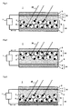
- Fig. 1 and Fig. 2 each schematically show the configuration of an existing dye-sensitized solar cell in which a stainless steel plate is used as the electrode.
- Fig. 1 is a type in which the electrode on the incident light side is a "counter electrode” for transmitting electrons to the ions in the solution; and
- Fig. 2 is a type in which the electrode on the incident light side is a "photoelectrode” having a semiconductor layer (photoelectric conversion layer).
- the light-transmissive electroconductive material 3 formed on the surface of the light-transmissive substrate 2 faces the stainless steel plate 4 to constitute the dye-sensitized solar cell 1.
- a semiconductor layer 6 is formed on the surface of the stainless steel plate 4.
- the semiconductor layer 6 is, for example, a porous layer formed by sintering oxide semiconductor particles of TiO 2 particles or the like having a large specific surface area, and the surface of the oxide semiconductor 7 carries a sensitizing dye 8 of ruthenium complex dye or the like.
- the stainless steel plate 4 and the semiconductor layer 6 existing on the surface thereof constitute the photoelectrode 40.
- the semiconductor layer 6 in the drawing conceptually shows the configuration of the oxide semiconductor 7 and the sensitizing dye 8 for convenience sake for illustration, and does not reflect directly the actual configuration of the semiconductor layer 6 (the same shall apply also to Fig. 2 and Fig. 3 ).
- the light-transmissive substrate 2 used is a glass plate, a PEN (polyethylene naphthalate) film or the like.
- the light-transmissive electroconductive material 3 is generally formed of a light-transmissive electroconductive film of ITO (indium-tin oxide), FTO (fluorine-doped tin oxide), TO (tin oxide) or the like.
- a catalyst thin-film layer 5 of platinum or the like On the surface of the light-transmissive electroconductive material 3, formed is a catalyst thin-film layer 5 of platinum or the like. In this case, the light-transmissive electroconductive material 3 and the catalyst thin-film layer 5 existing on the surface thereof constitute the counter electrode 30.
- the space between the catalyst thin-film layer 5 of the counter electrode 30 and the semiconductor layer 6 of the photoelectrode 40 is filled with an electrolytic solution 9 containing, for example, an iodide ion.
- an electrolytic solution 9 containing, for example, an iodide ion.
- a load 11 is connected to the counter electrode 30 and the photoelectrode 40 via a conductive wire, thereby forming a circuit.
- the sensitizing dye 8 is a ruthenium complex dye
- the electrolytic solution 9 is a solution containing an iodide ion
- the principle of cell operation is described briefly.
- the sensitizing dye (ruthenium complex dye) 8 absorbs the light and is excited, and the electron thereof is injected into the oxide semiconductor (TiO 2 ) 7.
- the sensitizing dye (ruthenium complex dye) 8 in the excited state receives the electron from the iodide ion I - in the electrolytic solution 9, and is restored to the ground state.
- I - is oxidized to be I 3 - , and diffuses toward the catalyst thin-film layer 5 of the counter electrode 30, then receives the electron from the side of the counter electrode 30, and is restored to I - .
- the electron moves in the route of sensitizing dye (ruthenium complex dye) 8 ⁇ oxide semiconductor (TiO 2 ) 7 ⁇ stainless steel plate 4 ⁇ load 11 ⁇ light-transmissive electroconductive material 3 ⁇ catalyst thin-film layer 5 ⁇ electrolytic solution 9 ⁇ sensitizing dye (ruthenium complex dye) 8.
- sensitizing dye ruthenium complex dye
- a stainless steel plate 4 is used as the counter electrode 30, and a light-transmissive electroconductive material 3 of ITO, FTO, TO or the like is used as the photoelectrode 40.
- the principle of current generation is basically the same as in the type of Fig. 1 .
- the electron moves in the route of sensitizing dye (ruthenium complex dye) 8 ⁇ oxide semiconductor (TiO 2 ) 7 ⁇ light-transmissive electroconductive material 3 ⁇ load 11 ⁇ stainless steel plate 4 ⁇ catalyst thin-film layer 5 ⁇ electrolytic solution 9 ⁇ sensitizing dye (ruthenium complex dye) 8.
- sensitizing dye ruthenium complex dye
- the present invention provides a technique of enhancing the photoelectric conversion efficiency of the dye-sensitized solar cell in which a stainless steel is used in one electrode.
- the photoelectrode of a dye-sensitized solar cell has a semiconductor layer as so mentioned above.
- the semiconductor layer is formed on an electroconductive substrate, and a current is taken out through the substrate.
- the stainless steel plate 4 and in the type of Fig. 2 the light-transmissive electroconductive material 3 each correspond to the above-mentioned electroconductive substrate.
- the present inventors have variously investigated and, as a result, have found that the adhesiveness between the semiconductor layer and the electroconductive substrate has a significant influence on the photoelectric conversion efficiency. When the adhesiveness between the semiconductor layer and the electroconductive substrate is increased, then the electric resistance at the joint part between the two decreases, which may contribute toward enhancing the photoelectric conversion efficiency.
- the present inventors have investigated in detail the cell configuration and, as a result, have found that, in the type of Fig. 1 , when a surface-roughened stainless steel plate having a specific surface profile is applied to the stainless steel plate 4 constituting the photoelectrode 40, then the adhesiveness between the semiconductor layer 6 and the stainless steel plate 4 is increased and the photoelectric conversion efficiency can be thereby enhanced more than before.
- Patent Reference 1 teaches that, as the stainless steel to be applied to the electrode material of a dye-sensitized solar cell, a type of steel having a Cr content of at least 17% by mass and an Mo content of at least 0.8% by mass should be selected. Afterwards, however, the present inventors have repeatedly investigated the cell taking the practicability thereof into consideration, and have found that a stainless steel having a Cr content of at least 16% by mass and an Mo content of at least 0.3% by mass is applicable to the electrode material of a dye-sensitized solar cell. On the basis of these findings, the inventors have completed the present invention.
- a dye-sensitized solar cell comprising a photoelectrode formed by using a stainless steel plate and a counter electrode formed by using a light-transmissive electroconductive material, wherein:
- the counter electrode is especially preferably one having visible light transmissiveness of such that the light transmittance at a wavelength of 500 nm is at least 55%.
- the catalyst to constitute the catalyst thin-film layer of the counter electrode there may be mentioned platinum, nickel or an electroconductive polymer.
- the thickness of the catalyst thin-film layer is from 0.5 to 5 nm.
- the thickness of the catalyst thin-film layer is from 1 to 10 nm.
- the roughened surface of the substrate stainless steel plate for use in the photoelectrode is especially preferably such that the part thereof at which the neighboring indentations join together has an edged boundary.
- the invention it has become possible to enhance the photoelectric conversion efficiency more than before in a dye-sensitized solar cell that uses a stainless steel plate in the electrode on one side thereof.
- a type of stainless steel in which the Cr content and the Mo content are smaller than before can be used in the electrode, and therefore the applicability of the invention is expected to the field where use of a more inexpensive type of steel is desired.
- Fig. 3 schematically shows the configuration of the dye-sensitized solar cell of the invention.
- the basic configuration of the cell and the current generation principle are the same as in Fig. 1 .
- the cell significantly differs in that the stainless steel plate 4 constituting the photoelectrode 40 has a roughened surface 10 on which the semiconductor layer 6 exists.
- a stainless steel plate of which the surface is roughened by forming pit-like indentations therein is used as the electroconductive substrate (a member to carry a semiconductor layer thereon and to act for electric current passage) of the photoelectrode.
- the pit-like indentations are those formed by chemical etching in an aqueous electrolytic solution to thereby form "pitting corrosion” a type of local corrosion, on the surface of the stainless steel plate.
- the surface that has been roughened by forming a large number of pit-like indentations therein exhibits an anchor effect for the semiconductor layer existing thereon, and contributes toward enhancing the adhesiveness between the stainless steel plate and the semiconductor layer.
- the pit-like indentations can be formed by etching in an aqueous electrolytic solution containing a ferric ion, as described below; however, even though the etching is promoted too much, the pitting corrosion may grow in the plate thickness direction (depth direction) and the boundary between the neighboring indentations may disappear in the plate thickness direction while the thickness thereof is reduced, and therefore, Ra does not increase indefinitely. Accordingly, it is unnecessary to define the uppermost limit of Ra, but in fact, the range of Ra may be from about 0.2 to 5 ⁇ m or so for readily attaining the photoelectric conversion efficiency-enhancing effect.
- the areal ratio in percentage of the pit-like indentations-formed part to the surface of the stainless steel plate is preferably at least 20% in terms of the projected areal ratio in percentage in the view of the roughened surface from directly above.
- the pit-like indentations may be formed in the entire surface of the steel plate, and the areal ratio of the pit-like indentations-formed part may be 100%.
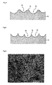
- Fig. 4 schematically illustrates the cross-section structure of a roughened surface in which the boundary between the neighboring indentations has a gentle slope.
- Indentations 60 are formed in the surface of the stainless steel plate 50, but the indentation boundary 70 has a gentle slope.
- the roughened surface profile of the type may be often formed when a stainless steel plate is etched in an aqueous electrolytic solution with no ferric ion therein, or when a stainless steel plate is surface-roughened by a physical removing means of polishing, shot blasting or the like.
- the anchor effect for the semiconductor layer would reduce and the effect of enhancing the adhesiveness may be insufficient. In such a case, the effect of enhancing the photoelectric conversion efficiency may also be poor.
- Fig. 5 schematically illustrates the cross-section structure of a roughened surface where the part at which the neighboring indentations join together has an edged boundary.
- This roughened surface profile is favorable for the stainless steel plate to be applied to the present invention.
- Indentations 60 are formed in the surface of the stainless steel plate 50, and the indentations are pit-like indentations. In the process where pitting corrosion grows in the depth direction, the opening diameter of the corrosion pit increases little by little, and the walls of the neighboring indentations 60 come to join together whereby the indentation boundary 70 becomes an edged boundary.
- the roughened surface profile of the type is attained by etching in an aqueous electrolytic solution with a ferric ion existing therein.
- edged boundary brings about an excellent anchor effect for the semiconductor layer, and the adhesiveness between the stainless steel plate and the semiconductor layer is thereby enhanced. As a result, the electric resistance at the joint part between the stainless steel plate and the semiconductor layer is reduced, and the photoelectric conversion efficiency is thereby significantly enhanced.
- Fig. 6 shows one example of a SEM photograph of the roughened surface of a surface-roughened stainless steel plate applicable to the dye-sensitized solar cell of the invention. An edged boundary is observed between the neighboring pit-like indentations.
- the stainless steel plate to be applied to the electroconductive substrate of the photoelectrode in the invention a type of stainless steel that has excellent resistance to the electrolytic solution in the dye-sensitized solar cell must be employed.
- a type of stainless steel containing Cr in an amount of at least 16% by mass and Mo in an amount of at least 0.3% by mass it has been found that when a type of stainless steel containing Cr in an amount of at least 16% by mass and Mo in an amount of at least 0.3% by mass is used, a practicable dye-sensitized solar cell can be constructed.
- stainless steel is said to be poor in corrosion resistance to an aqueous solution containing a chloride ion Cl - , and for enhancing the corrosion resistance, increase in Cr and addition of Mo are said to be effective.
- ferritic SUS444 suitable to water heaters secures a Cr content of at least 17% by mass and an Mo content of at least 1.75% by mass; and even SUS316, a highly corrosion-resistant, general-purpose austenitic steel secures a Cr content of at least 16% by mass and an Mo content of at least 2% by mass.
- the conversion efficiency retention is at least 90%, more preferably at least 95%.
- a type of stainless steel containing Cr in an amount of at least 16% by mass and Mo in an amount of at least 0.3% by mass is employed, then a dye-sensitized solar cell having a conversion efficiency retention of at least 80% can be constructed sufficiently.
- the Cr content is preferably at least 17% by mass.
- the Mo content is preferably at least 0.5% by mass, and may be controlled to fall within a range of at least 0.8% by mass, or at least 1.0% by mass.
- the uppermost limit of Cr may be 32% by mass, and may be controlled to fall within a component range of at most 25% by mass.
- the uppermost limit of Mo may be 3% by mass, and may be controlled to fall within a component range of at most 2% by mass.
- the specific roughened surface profile mentioned as above can be formed by etching a stainless steel plate of which the surface is not roughened, for example, an ordinary annealed/acid-pickled steel, a BA-annealed steel, a skin-pass finished steel or the like, in an aqueous solution with a ferric ion existing therein.
- etching for example, employable is a method of dipping and soaking in a liquid, a method of alternating electrolysis in a liquid or the like.
- ferric chloride (FeCl 3 ) is favorably used as the ferric ion source.
- a method of etching in a mixed aqueous solution of ferric chloride (FeCl 3 ) and hydrochloric acid (HCl) is extremely effective.
- FeCl 3 ferric chloride
- HC1 hydrochloric acid
- the temperature is from 35 to 70°C
- the dipping time is from 3 to 120 seconds
- a condition to give a roughened surface having pit-like indentations and having Ra of at least 0.2 ⁇ m can be found out.
- an aqueous solution of ferric chloride is used as the electrolytic solution, and within a condition range where the Fe 3+ ion concentration is from 1 to 50 g/L, the temperature is from 30 to 70°C, the anode electrolytic current density is from 1.0 to 10.0 kA/m 2 , the cathode electrolytic current density is from 0.1 to 3.0 kA/m 2 , an alternating electrolysis cycle is from 1 to 20 Hz and an electrolysis time is from 10 to 300 seconds, a condition to give a roughened surface having pit-like indentations and having Ra of at least 0.2 ⁇ m can be found out.
- the power-on time in one cycle may be long and the size of the pit-like indentations can be thereby enlarged; but on the contrary, when the alternating electrolysis cycle is prolonged, then the size of the pit-like indentations can be reduced.
- the photoelectrode can be produced, for example, according to the method mentioned below.
- a coating material paste or liquid
- a coating film is applied on the roughened surface of the above-mentioned, surface-roughened stainless steel plate, and dried to form a coating film thereon.
- the coating film is fired to sinter the oxide particles, thereby forming a porous semiconductor layer.
- the coated stainless steel plate is put in a heating furnace and is kept therein at a temperature at which the particles could be sintered suitably (for example, at 400 to 600°C).
- the oxide semiconductor TiO 2 is generally used, but ZnO, SnO 2, ZrO 2 or the like may also be used. These oxides may be combined and used here.
- the porous semiconductor layer is dipped in an organic solvent with a sensitizing dye dispersed therein, thereby making the semiconductor layer carry the sensitizing dye.
- the coated stainless steel plate may be dipped in the organic solvent.
- the sensitizing dye typically used here is ruthenium complex dye.
- the counter electrode may be produced by making a light-transmissive electroconductive material held on the surface of a light-transmissive substrate such as a glass plate, a PEN (polyethylene naphthalate) film or the like followed by forming a catalyst thin-film layer on the surface of the light-transmissive electroconductive material.
- a light-transmissive electroconductive material herein usable is an electroconductive film of ITO (indium-tin oxide), FTO (fluorine-doped tin oxide), TO (tin oxide) or the like.
- the catalyst thin-film layer preferred for use herein is a metal film of platinum, nickel or the like, or an electroconductive polymer film of polyaniline, polyethylenedioxythiophene or the like.
- the metal film may be formed, for example, according to a sputtering method.
- the electroconductive polymer film may be formed, for example, according to a spin coating method.
- the counter electrode has visible light transmissiveness of such that the light transmittance at a wavelength of 500 nm is at least 55%. In this case, a high photoelectric conversion efficiency can be obtained.
- the light transmittance varies depending on the thickness of the catalyst thin-film layer. A thinner catalyst thin-film layer may have a higher transmittance. However, when the catalyst thin-film layer is thinned too much, the photoelectric conversion efficiency may lower owing to the reduction in the catalytic effect.
- the thickness of the catalyst thin-film layer is controlled to fall within a range of from 0.5 to 5 nm.
- the thickness of the catalyst thin-film layer is controlled to fall within a range of from 1 to 10 nm.
- the above-mentioned photoelectrode and counter electrode are so arranged that the semiconductor layer of the photoelectrode could face the catalyst thin-film layer of the counter electrode via an electrolytic solution put therebetween, thereby constructing the dye-sensitized solar cell of the present invention.
- a stainless steel ingot having the composition shown in Table 1 was produced, and worked into a cold-rolled annealed steel plate having a thickness of 0.2 mm (No. 2D finish) according to an ordinary stainless steel plate production process.
- ⁇ means a ferritic type
- ⁇ means an austenitic type.
- - (hyphen) means lower than the detectable limit in ordinary analysis in steel production sites.
- a sample cut out of the above-mentioned steel plate was surface-roughened by dipping and soaking or by alternating electrolysis, thereby preparing test samples. Some test samples that had not been surface-roughened to be as yet merely No. 2D finish were also prepared. In Table 2, those processed by dipping and soaking are represented by "dipping"; and those processed by alternating electrolysis are by "electrolysis”.
- the surface roughening treatment by dipping and soaking was attained according to a method of dipping the test piece in an aqueous mixed solution of ferric chloride + hydrochloric acid having an Fe 3+ ion concentration of 30 g/L and an HCl concentration of 30 g/L at a temperature of 50°C, for 40 seconds.
- the surface roughening treatment by alternating electrolysis was attained in an aqueous ferric chloride solution having an Fe 3+ ion concentration of from 5 to 50 g/L at a temperature of from 35 to 65°C, under the condition where the anode electrolysis current density was 3 kA/m 2 , the cathode electrolysis current density was 0.3 kA/m 2 , the alternating electrolysis cycle was 10 Hz and the electrolysis time was from 10 to 120 seconds.
- the roughened surfaces obtained herein all had pit-like indentations in an areal ratio in percentage of at least 20%, and that the part at which the neighboring indentations joined together had an edged boundary.
- a TiO 2 paste (Peccel Technologies' PECC-01-06).
- the TiO 2 paste was applied onto the surface of the above-mentioned sample (in case where the sample had been surface-roughened, the paste was applied onto the roughened surface thereof) according to a doctor blade method, and dried to thereby form a TiO 2 -containing coating film thereon.
- the film-coated substrate, stainless steel plate was put into an oven at 450°C and fired therein, thereby sinter the TiO 2 particles to form a semiconductor layer.
- the mean thickness of the thus-formed semiconductor layer was 10 ⁇ m.
- ruthenium complex dye (Peccel Technologies' PECD-07) was used, and this was dispersed in a mixed solvent of acetonitrile and tert-butanol to prepare a dye dispersion.
- the above-mentioned, semiconductor layer-coated stainless steel plate was dipped in the dye dispersion, thereby producing a photoelectrode having the sensitizing dye carried by the semiconductor layer thereof.
- the light-transmissive electroconductive material for a counter electrode prepared was "ITO-PEN film” having an ITO film formed on a PEN film substrate (Peccel Technologies' PECF-IP). This was set in a sputtering apparatus, and a target of platinum was sputtered thereonto for 1 minute to form a platinum catalyst thin-film layer on the ITO film, thereby producing a counter electrode. In this case, the thickness of the platinum was about 3 nm.
- the above-mentioned photoelectrode and counter electrode were combined between a heat-sealable film (Peccel Technologies' Surlyn Film" as arranged therebetween to surround a part to be a cell, thereby producing a cell structure in which the distance between the stainless steel surface of the photoelectrode and the counter electrode was 50 ⁇ m.
- the cell structure was hot-compressed with a hot presser to seal up the cell, and further an epoxy resin was applied to the periphery of the cell and cured therearound.
- an electrolytic solution (Peccel Technologies' PECE-K01) was injected into the cell with a microsyringe. Subsequently, the electrolytic solution introducing mouth was sealed up with an epoxy resin, thereby constructing a dye-sensitized solar cell.
- the conversion efficiency of the thus-constructed, dye-sensitized solar cell was measured according to the process mentioned below.
- a solar simulator Yamashita Denso's YSS-100
- the dye-sensitized solar cell was tested for the I-V characteristic thereof by the use of a source meter, Keithley' s 2400 Model, while irradiated with pseudo-sunlight at AM 1.5 and at 100 mW/cm 2 from the side of the counter electrode thereof, from which the short-circuit current JSC, the open voltage VOC and the form factor FF were obtained. From these values, the photoelectric conversion efficiency ⁇ was computed according to the following formula (1).
- Photoelectric Conversion Efficiency ⁇ % short - circuit current JSC mA / cm 2 ⁇ open voltage VOC V ⁇ fill factor FF / incident light 100 mW / cm 2 ⁇ 100
- the initial photoelectric conversion efficiency as measured immediately after the cell construction, is represented by ⁇ 0 (%).
- ⁇ 0 (%) After measurement of ⁇ 0 (%), the solar cell was left in a thermostat at 65°C for 100 hours. Subsequently, the photoelectric conversion efficiency of the cell was measured in the same manner as above.
- a stainless steel plate having a low Mo content is used in Test Nos. 1 to 5 of comparative samples, and the photoelectric conversion efficiency after left at 65°C for 100 hours of the samples was extremely low and the conversion efficiency retention thereof was also low. This may be considered because the corrosion resistance of the steel plate in the electrolytic solution was poor and therefore Fe and Cr of the stainless steel ingredients dissolved out in the electrolytic solution.
- Test Nos. 6 to 8 an un-roughened stainless steel plate was used and therefore, the adhesiveness between the stainless steel plate of the photoelectrode and the semiconductor layer would be low, and the photoelectric conversion efficiency ⁇ 0 and ⁇ 1 of the samples were both low.
- Test No. 11 (Steel G) in Table 2 produced according to the same method as in Example 1 was prepared.
- the counter electrode was produced as follows: Platinum, nickel or polyaniline as the catalyst, and the thickness of the catalyst thin-film layer was changed variously as described below.
- an ITO film was formed on the PEN film substrate to prepare "ITO-PEN film".
- the catalyst thin-film layer was formed using a sputtering apparatus like in Example 1, and the film thickness was controlled by changing the sputtering time.
Landscapes
- Chemical & Material Sciences (AREA)
- Engineering & Computer Science (AREA)
- Materials Engineering (AREA)
- Metallurgy (AREA)
- Organic Chemistry (AREA)
- Mechanical Engineering (AREA)
- Chemical Kinetics & Catalysis (AREA)
- General Chemical & Material Sciences (AREA)
- Electrochemistry (AREA)
- Physics & Mathematics (AREA)
- Thermal Sciences (AREA)
- Crystallography & Structural Chemistry (AREA)
- Power Engineering (AREA)
- Microelectronics & Electronic Packaging (AREA)
- Hybrid Cells (AREA)
- Photovoltaic Devices (AREA)
Abstract
Description
- The present invention relates to a dye-sensitized solar cell in which stainless steel is used as the constitutive material of the photoelectrode (negative electrode), and to its production method.
- The mainstream of solar cells is toward those in which silicon is used as the photoelectric conversion element; however, as more economical next-generation solar cells in lieu of those, practical use of "dye-sensitized solar cells" is now under study. The dye-sensitized solar cell must be so designed that external light could reach the sensitizing dye carried inside the "photoelectrode" (inside the cell) therein, and therefore, the electroconductive member of the electrode to be on the incident light side must be formed of a light-transmissive electroconductive material. On the other hand, the material to constitute the electrode on the side opposite to the incident light side does not necessarily have to be light-transmissive, for which, therefore, use of a metal material of good electroconductivity is advantageous. Recently, as the metal material of the type, applicability of stainless steel that is a relatively inexpensive corrosion-resistant material has been confirmed, and accordingly, cost reduction of dye-sensitized solar cells is expected.
Patent Reference 1 discloses a dye-sensitized solar cell in which a stainless steel plate is used as the electrode on the side opposite to the incident light side therein. -
Fig. 1 and Fig. 2 each schematically show the configuration of an existing dye-sensitized solar cell in which a stainless steel plate is used as the electrode.Fig. 1 is a type in which the electrode on the incident light side is a "counter electrode" for transmitting electrons to the ions in the solution; andFig. 2 is a type in which the electrode on the incident light side is a "photoelectrode" having a semiconductor layer (photoelectric conversion layer). - In the type of
Fig. 1 , the light-transmissiveelectroconductive material 3 formed on the surface of the light-transmissive substrate 2 faces the stainless steel plate 4 to constitute the dye-sensitizedsolar cell 1. - A
semiconductor layer 6 is formed on the surface of the stainless steel plate 4. Thesemiconductor layer 6 is, for example, a porous layer formed by sintering oxide semiconductor particles of TiO2 particles or the like having a large specific surface area, and the surface of theoxide semiconductor 7 carries asensitizing dye 8 of ruthenium complex dye or the like. In this case, the stainless steel plate 4 and thesemiconductor layer 6 existing on the surface thereof constitute thephotoelectrode 40. Thesemiconductor layer 6 in the drawing conceptually shows the configuration of theoxide semiconductor 7 and thesensitizing dye 8 for convenience sake for illustration, and does not reflect directly the actual configuration of the semiconductor layer 6 (the same shall apply also toFig. 2 and Fig. 3 ). On the other hand, as the light-transmissive substrate 2, used is a glass plate, a PEN (polyethylene naphthalate) film or the like. The light-transmissiveelectroconductive material 3 is generally formed of a light-transmissive electroconductive film of ITO (indium-tin oxide), FTO (fluorine-doped tin oxide), TO (tin oxide) or the like. On the surface of the light-transmissiveelectroconductive material 3, formed is a catalyst thin-film layer 5 of platinum or the like. In this case, the light-transmissiveelectroconductive material 3 and the catalyst thin-film layer 5 existing on the surface thereof constitute thecounter electrode 30. The space between the catalyst thin-film layer 5 of thecounter electrode 30 and thesemiconductor layer 6 of thephotoelectrode 40 is filled with an electrolytic solution 9 containing, for example, an iodide ion. Outside the dye-sensitizedsolar cell 1, aload 11 is connected to thecounter electrode 30 and thephotoelectrode 40 via a conductive wire, thereby forming a circuit. - With reference to an example where the
oxide semiconductor 7 is TiO2, thesensitizing dye 8 is a ruthenium complex dye, and the electrolytic solution 9 is a solution containing an iodide ion, the principle of cell operation is described briefly. When theincident light 20 has reached the sensitizing dye (ruthenium complex dye) 8, thesensitizing dye 8 absorbs the light and is excited, and the electron thereof is injected into the oxide semiconductor (TiO2) 7. The sensitizing dye (ruthenium complex dye) 8 in the excited state receives the electron from the iodide ion I- in the electrolytic solution 9, and is restored to the ground state. I- is oxidized to be I3 -, and diffuses toward the catalyst thin-film layer 5 of thecounter electrode 30, then receives the electron from the side of thecounter electrode 30, and is restored to I-. Accordingly, the electron moves in the route of sensitizing dye (ruthenium complex dye) 8 → oxide semiconductor (TiO2) 7 → stainless steel plate 4 →load 11 → light-transmissiveelectroconductive material 3 → catalyst thin-film layer 5 → electrolytic solution 9 → sensitizing dye (ruthenium complex dye) 8. As a result, a current to put theload 11 in action is generated. - In the type of
Fig. 2 , a stainless steel plate 4 is used as thecounter electrode 30, and a light-transmissiveelectroconductive material 3 of ITO, FTO, TO or the like is used as thephotoelectrode 40. The principle of current generation is basically the same as in the type ofFig. 1 . In this case, the electron moves in the route of sensitizing dye (ruthenium complex dye) 8 → oxide semiconductor (TiO2) 7 → light-transmissiveelectroconductive material 3 →load 11 → stainless steel plate 4 → catalyst thin-film layer 5 → electrolytic solution 9 → sensitizing dye (ruthenium complex dye) 8. As a result, a current to put theload 11 in action is generated. -
- Patent Reference 1:
JP-A-2008-34110 - In the dye-sensitized solar cell of the type of
Fig. 1 and Fig. 2 , a stainless steel plate is used in one electrode to thereby realize cost reduction and electroconductivity enhancement. However, for further popularization of dye-sensitized solar cells, it is desired to further enhance the photoelectric conversion efficiency of the cells. To satisfy the requirement, the present invention provides a technique of enhancing the photoelectric conversion efficiency of the dye-sensitized solar cell in which a stainless steel is used in one electrode. - The photoelectrode of a dye-sensitized solar cell has a semiconductor layer as so mentioned above. In general, the semiconductor layer is formed on an electroconductive substrate, and a current is taken out through the substrate. In the type of
Fig. 1 , the stainless steel plate 4, and in the type ofFig. 2 , the light-transmissiveelectroconductive material 3 each correspond to the above-mentioned electroconductive substrate. The present inventors have variously investigated and, as a result, have found that the adhesiveness between the semiconductor layer and the electroconductive substrate has a significant influence on the photoelectric conversion efficiency. When the adhesiveness between the semiconductor layer and the electroconductive substrate is increased, then the electric resistance at the joint part between the two decreases, which may contribute toward enhancing the photoelectric conversion efficiency. The present inventors have investigated in detail the cell configuration and, as a result, have found that, in the type ofFig. 1 , when a surface-roughened stainless steel plate having a specific surface profile is applied to the stainless steel plate 4 constituting thephotoelectrode 40, then the adhesiveness between thesemiconductor layer 6 and the stainless steel plate 4 is increased and the photoelectric conversion efficiency can be thereby enhanced more than before. -
Patent Reference 1 teaches that, as the stainless steel to be applied to the electrode material of a dye-sensitized solar cell, a type of steel having a Cr content of at least 17% by mass and an Mo content of at least 0.8% by mass should be selected. Afterwards, however, the present inventors have repeatedly investigated the cell taking the practicability thereof into consideration, and have found that a stainless steel having a Cr content of at least 16% by mass and an Mo content of at least 0.3% by mass is applicable to the electrode material of a dye-sensitized solar cell.
On the basis of these findings, the inventors have completed the present invention. - Specifically, in the invention, there is provided a dye-sensitized solar cell comprising a photoelectrode formed by using a stainless steel plate and a counter electrode formed by using a light-transmissive electroconductive material, wherein:
- the photoelectrode comprises, as the substrate thereof, a stainless steel plate of a type of stainless steel having a chemical composition of any of the following (A) to (D) and having a roughened surface in which pit-like indentations are formed and which is controlled to have an arithmetic average roughness Ra of at least 0.2 µm, and comprises, as formed on the roughened surface of the substrate, a sensitizing dye-carrying semiconductor layer;
- the counter electrode has a catalyst thin-film layer formed on the surface of the light-transmissive electroconductive material and has visible light transmissiveness; and
- the semiconductor layer of the photoelectrode and the catalyst thin-film layer of the counter electrode face each other via an electrolytic solution.
-
- (A) One corresponding to a ferritic stainless steel containing Cr: at least 16% by mass and Mo: at least 0.3% by mass and defined by JIS G4305:2005.
- (B) One corresponding to an austenitic stainless steel containing Cr: at least 16% by mass and Mo: at least 0.3% by mass and defined by JIS G4305:2005.
- (C) A ferritic stainless steel comprising, by mass, C: at most 0.15%, Si: at most 1.2%, Mn: at most 1.2%, P: at most 0.04%, S: at most 0.03%, Ni: at most 0.6%, Cr: from 16 to 32%, Mo: from 0.3 to 3%, Cu: from 0 to 1%, Nb: from 0 to 1%, Ti: from 0 to 1%, Al: from 0 to 0.2%, N: at most 0.025%, B: from 0 to 0.01%, with a balance of Fe and inevitable impurities.
- (D) An austenitic stainless steel comprising, by mass, C: at most 0.15%, Si: at most 4%, Mn: at most 2.5%, P: at most 0.045%, S: at most 0.03%, Ni: from 6 to 28%, Cr: from 16 to 32%, Mo: from 0.3 to 7%, Cu: from 0 to 3.5%, Nb: from 0 to 1%, Ti: from 0 to 1%, A1: from 0 to 0.1%, N: at most 0.3%, B: from 0 to 0.01%, with a balance of Fe and inevitable impurities.
- In the above-mentioned dye-sensitized solar cell, the counter electrode is especially preferably one having visible light transmissiveness of such that the light transmittance at a wavelength of 500 nm is at least 55%. As the catalyst to constitute the catalyst thin-film layer of the counter electrode, there may be mentioned platinum, nickel or an electroconductive polymer. In case where the catalyst is platinum or nickel, preferably, the thickness of the catalyst thin-film layer is from 0.5 to 5 nm. In case where the catalyst is an electroconductive polymer, preferably, the thickness of the catalyst thin-film layer is from 1 to 10 nm.
- The roughened surface of the substrate stainless steel plate for use in the photoelectrode is especially preferably such that the part thereof at which the neighboring indentations join together has an edged boundary.
- In the invention, there is also provided a method for producing the above-mentioned dye-sensitized solar cell, including:
- a step of etching a stainless steel plate in an aqueous solution with a ferric ion existing therein to form pit-like indentations in the plate, thereby giving a substrate that has a roughened surface with an arithmetic average roughness Ra of at least 0.2 µm,
- a step of forming, on the roughened surface, a coating film that contains oxide semiconductor particles,
- a step of firing the coating film to form a porous semiconductor layer,
- a step of dipping the semiconductor layer in a solvent with a sensitizing dye dispersed therein to make the semiconductor layer carry the sensitizing dye, thereby giving a photoelectrode that comprises the sensitizing dye-carrying semiconductor layer on the roughened surface of the substrate stainless steel plate, and
- a step of arranging the photoelectrode and the visible light-transmissive counter electrode with the catalyst thin-film layer formed on the surface of the light-transmissive electroconductive material, in such a manner that the semiconductor layer of the photoelectrode could face the catalyst thin-film layer of the counter electrode, and introducing an electrolytic solution into the space between the two electrodes.
- According to the invention, it has become possible to enhance the photoelectric conversion efficiency more than before in a dye-sensitized solar cell that uses a stainless steel plate in the electrode on one side thereof. In the dye-sensitized solar cell of the invention, a type of stainless steel in which the Cr content and the Mo content are smaller than before can be used in the electrode, and therefore the applicability of the invention is expected to the field where use of a more inexpensive type of steel is desired.
-
- [
Fig. 1 ] A view schematically showing the configuration of an existing dye-sensitized solar cell where a stainless steel plate is used in the photoelectrode. - [
Fig. 2 ] A view schematically showing the configuration of an existing dye-sensitized solar cell where a stainless steel plate is used in the counter electrode. - [
Fig. 3 ] A view schematically showing the configuration of the dye-sensitized solar cell of the invention. - [
Fig. 4 ] A view schematically illustrating the cross-section structure of a roughened surface in which the boundary between the neighboring indentations has a gentle slope. - [
Fig. 5 ] A view schematically illustrating the cross-section structure of a roughened surface where the part at which the neighboring indentations join together has an edged boundary. - [
Fig. 6 ] One example of a SEM photograph of the roughened surface of a stainless steel plate in which pit-like indentations are formed by etching in an aqueous, ferric ion-containing solution. -
Fig. 3 schematically shows the configuration of the dye-sensitized solar cell of the invention. The basic configuration of the cell and the current generation principle are the same as inFig. 1 . However, the cell significantly differs in that the stainless steel plate 4 constituting thephotoelectrode 40 has a roughened surface 10 on which thesemiconductor layer 6 exists. - In the invention, a stainless steel plate of which the surface is roughened by forming pit-like indentations therein is used as the electroconductive substrate (a member to carry a semiconductor layer thereon and to act for electric current passage) of the photoelectrode. The pit-like indentations are those formed by chemical etching in an aqueous electrolytic solution to thereby form "pitting corrosion" a type of local corrosion, on the surface of the stainless steel plate. The surface that has been roughened by forming a large number of pit-like indentations therein exhibits an anchor effect for the semiconductor layer existing thereon, and contributes toward enhancing the adhesiveness between the stainless steel plate and the semiconductor layer. Accordingly, the bonding force between the two is increased and the contact area is also increased, and as a result, the electric resistance in the bonding interface between the two is thereby reduced. As a result of various investigations, an increase in the photoelectric conversion efficiency is clearly recognized in the case of using a stainless steel plate of which the roughened surface with pit-like indentations formed therein has an arithmetic average roughness Ra of at least 0.2 µm. In case where Ra is smaller than the range, the above-mentioned effect would be insufficient and it would be difficult to significantly and stably increase the photoelectric conversion efficiency. The pit-like indentations can be formed by etching in an aqueous electrolytic solution containing a ferric ion, as described below; however, even though the etching is promoted too much, the pitting corrosion may grow in the plate thickness direction (depth direction) and the boundary between the neighboring indentations may disappear in the plate thickness direction while the thickness thereof is reduced, and therefore, Ra does not increase indefinitely. Accordingly, it is unnecessary to define the uppermost limit of Ra, but in fact, the range of Ra may be from about 0.2 to 5 µm or so for readily attaining the photoelectric conversion efficiency-enhancing effect.
- The areal ratio in percentage of the pit-like indentations-formed part to the surface of the stainless steel plate is preferably at least 20% in terms of the projected areal ratio in percentage in the view of the roughened surface from directly above. The pit-like indentations may be formed in the entire surface of the steel plate, and the areal ratio of the pit-like indentations-formed part may be 100%.
-
Fig. 4 schematically illustrates the cross-section structure of a roughened surface in which the boundary between the neighboring indentations has a gentle slope.Indentations 60 are formed in the surface of thestainless steel plate 50, but theindentation boundary 70 has a gentle slope. The roughened surface profile of the type may be often formed when a stainless steel plate is etched in an aqueous electrolytic solution with no ferric ion therein, or when a stainless steel plate is surface-roughened by a physical removing means of polishing, shot blasting or the like. In case where theindentation boundary 70 is excessively gentle, the anchor effect for the semiconductor layer would reduce and the effect of enhancing the adhesiveness may be insufficient. In such a case, the effect of enhancing the photoelectric conversion efficiency may also be poor. -
Fig. 5 schematically illustrates the cross-section structure of a roughened surface where the part at which the neighboring indentations join together has an edged boundary. This roughened surface profile is favorable for the stainless steel plate to be applied to the present invention.Indentations 60 are formed in the surface of thestainless steel plate 50, and the indentations are pit-like indentations. In the process where pitting corrosion grows in the depth direction, the opening diameter of the corrosion pit increases little by little, and the walls of the neighboringindentations 60 come to join together whereby theindentation boundary 70 becomes an edged boundary. The roughened surface profile of the type is attained by etching in an aqueous electrolytic solution with a ferric ion existing therein. The presence of the edged boundary brings about an excellent anchor effect for the semiconductor layer, and the adhesiveness between the stainless steel plate and the semiconductor layer is thereby enhanced. As a result, the electric resistance at the joint part between the stainless steel plate and the semiconductor layer is reduced, and the photoelectric conversion efficiency is thereby significantly enhanced. -
Fig. 6 shows one example of a SEM photograph of the roughened surface of a surface-roughened stainless steel plate applicable to the dye-sensitized solar cell of the invention. An edged boundary is observed between the neighboring pit-like indentations. - As the stainless steel plate to be applied to the electroconductive substrate of the photoelectrode in the invention, a type of stainless steel that has excellent resistance to the electrolytic solution in the dye-sensitized solar cell must be employed. As a result of detailed investigations made by the present inventors, it has been found that when a type of stainless steel containing Cr in an amount of at least 16% by mass and Mo in an amount of at least 0.3% by mass is used, a practicable dye-sensitized solar cell can be constructed.
- In general, stainless steel is said to be poor in corrosion resistance to an aqueous solution containing a chloride ion Cl-, and for enhancing the corrosion resistance, increase in Cr and addition of Mo are said to be effective. For example, ferritic SUS444 suitable to water heaters secures a Cr content of at least 17% by mass and an Mo content of at least 1.75% by mass; and even SUS316, a highly corrosion-resistant, general-purpose austenitic steel secures a Cr content of at least 16% by mass and an Mo content of at least 2% by mass. However, there are known few reports relating to the corrosion resistance of stainless steel to iodide ion, and in particular, any substantial investigation relating to the use for photoelectrodes in dye-sensitized solar cells is not as yet made sufficiently. Given the situation, the present inventors have made detailed investigations and have known that a dye-sensitized solar cell, which is so designed that the change of the photoelectric conversion efficiency η1 (%) of the cell thereof, as measured after left at 65°C for 100 hours, relative to the initial photoelectric conversion efficiency η0 (%), as measured immediately after its construction, (conversion efficiency retention to be represented by the following formula (2)) could be at least 80%, can be evaluated to have practical-level durability in applications where the cell is incorporated in everyday-application products for personal use. Preferably, the conversion efficiency retention is at least 90%, more preferably at least 95%. After further investigations made by the inventors, it has been clarified that, when a type of stainless steel containing Cr in an amount of at least 16% by mass and Mo in an amount of at least 0.3% by mass is employed, then a dye-sensitized solar cell having a conversion efficiency retention of at least 80% can be constructed sufficiently.
- Concretely, the above-mentioned types of stainless steel (A) to (D) are mentioned to be preferred ones for use herein. For further better corrosion resistance, the Cr content is preferably at least 17% by mass. The Mo content is preferably at least 0.5% by mass, and may be controlled to fall within a range of at least 0.8% by mass, or at least 1.0% by mass. The uppermost limit of Cr may be 32% by mass, and may be controlled to fall within a component range of at most 25% by mass. The uppermost limit of Mo may be 3% by mass, and may be controlled to fall within a component range of at most 2% by mass.
- The specific roughened surface profile mentioned as above can be formed by etching a stainless steel plate of which the surface is not roughened, for example, an ordinary annealed/acid-pickled steel, a BA-annealed steel, a skin-pass finished steel or the like, in an aqueous solution with a ferric ion existing therein. For the etching, for example, employable is a method of dipping and soaking in a liquid, a method of alternating electrolysis in a liquid or the like. In any case, ferric chloride (FeCl3) is favorably used as the ferric ion source.
- In the case of dipping and soaking, a method of etching in a mixed aqueous solution of ferric chloride (FeCl3) and hydrochloric acid (HCl) is extremely effective. Concretely, for example, within a condition range where the Fe3+ ion concentration is from 15 to 100 g/L, the HC1 concentration is from 20 to 200 g/L, the temperature is from 35 to 70°C and the dipping time is from 3 to 120 seconds, a condition to give a roughened surface having pit-like indentations and having Ra of at least 0.2 µm can be found out.
- In the case of alternating electrolysis, for example, an aqueous solution of ferric chloride is used as the electrolytic solution, and within a condition range where the Fe3+ ion concentration is from 1 to 50 g/L, the temperature is from 30 to 70°C, the anode electrolytic current density is from 1.0 to 10.0 kA/m2, the cathode electrolytic current density is from 0.1 to 3.0 kA/m2, an alternating electrolysis cycle is from 1 to 20 Hz and an electrolysis time is from 10 to 300 seconds, a condition to give a roughened surface having pit-like indentations and having Ra of at least 0.2 µm can be found out. When the alternating electrolysis cycle is reduced, then the power-on time in one cycle may be long and the size of the pit-like indentations can be thereby enlarged; but on the contrary, when the alternating electrolysis cycle is prolonged, then the size of the pit-like indentations can be reduced.
- The photoelectrode can be produced, for example, according to the method mentioned below. First, a coating material (paste or liquid) containing oxide semiconductor particles is applied on the roughened surface of the above-mentioned, surface-roughened stainless steel plate, and dried to form a coating film thereon. Subsequently, the coating film is fired to sinter the oxide particles, thereby forming a porous semiconductor layer. For the firing, the coated stainless steel plate is put in a heating furnace and is kept therein at a temperature at which the particles could be sintered suitably (for example, at 400 to 600°C). As the oxide semiconductor, TiO2 is generally used, but ZnO, SnO2, ZrO2 or the like may also be used. These oxides may be combined and used here. Thus formed, the porous semiconductor layer is dipped in an organic solvent with a sensitizing dye dispersed therein, thereby making the semiconductor layer carry the sensitizing dye. The coated stainless steel plate may be dipped in the organic solvent. As the sensitizing dye, typically used here is ruthenium complex dye.
- The counter electrode may be produced by making a light-transmissive electroconductive material held on the surface of a light-transmissive substrate such as a glass plate, a PEN (polyethylene naphthalate) film or the like followed by forming a catalyst thin-film layer on the surface of the light-transmissive electroconductive material. As the light-transmissive electroconductive material, herein usable is an electroconductive film of ITO (indium-tin oxide), FTO (fluorine-doped tin oxide), TO (tin oxide) or the like. As the catalyst thin-film layer, preferred for use herein is a metal film of platinum, nickel or the like, or an electroconductive polymer film of polyaniline, polyethylenedioxythiophene or the like. The metal film may be formed, for example, according to a sputtering method. The electroconductive polymer film may be formed, for example, according to a spin coating method. Especially preferably, the counter electrode has visible light transmissiveness of such that the light transmittance at a wavelength of 500 nm is at least 55%. In this case, a high photoelectric conversion efficiency can be obtained. The light transmittance varies depending on the thickness of the catalyst thin-film layer. A thinner catalyst thin-film layer may have a higher transmittance. However, when the catalyst thin-film layer is thinned too much, the photoelectric conversion efficiency may lower owing to the reduction in the catalytic effect. As a result of various investigations made by the inventors, it has been found that, in case where the catalyst is platinum or nickel, preferably, the thickness of the catalyst thin-film layer is controlled to fall within a range of from 0.5 to 5 nm. In case where the catalyst is polyaniline, preferably, the thickness of the catalyst thin-film layer is controlled to fall within a range of from 1 to 10 nm.
- The above-mentioned photoelectrode and counter electrode are so arranged that the semiconductor layer of the photoelectrode could face the catalyst thin-film layer of the counter electrode via an electrolytic solution put therebetween, thereby constructing the dye-sensitized solar cell of the present invention.
- A stainless steel ingot having the composition shown in Table 1 was produced, and worked into a cold-rolled annealed steel plate having a thickness of 0.2 mm (No. 2D finish) according to an ordinary stainless steel plate production process. In the column of morphology in Table 1, "α" means a ferritic type, and "γ" means an austenitic type. In the Table, "-" (hyphen) means lower than the detectable limit in ordinary analysis in steel production sites.
- [Table 1]
Table 1 Group Steel Chemical Composition (% by mass) Morphology C Si Mn P S Ni Cr Mo Cu Nb Ti Al Comparative Steel A 0.069 0.51 0.34 0.032 0.005 0.14 16.13 0.11 0.04 - 0.004 - α B 0.014 0.42 0.58 0.028 0.003 0.16 17.25 0.02 0.06 0.40 - 0.007 C 0.070 0.54 0.79 0.035 0.006 8.04 18.12 0.20 0.31 - - - γ D 0.062 0.56 1.52 0.025 0.001 19.08 25.50 0.24 0.13 0.03 - 0.006 Steel for the Invention E 0.007 0.48 0.09 0.024 0.001 0.10 16.25 0.33 0.02 - 0.270 0.087 α F 0.003 0.09 0.09 0.032 0.001 0.10 17.52 0.87 - - 0.180 0.071 G 0.006 0.20 0.13 0.030 0.001 0.11 22.14 1.12 0.02 0.20 0.204 0.074 H 0.017 0.53 1.74 0.027 0.002 12.58 17.22 2.73 0.34 - - - γ - A sample cut out of the above-mentioned steel plate was surface-roughened by dipping and soaking or by alternating electrolysis, thereby preparing test samples. Some test samples that had not been surface-roughened to be as yet merely No. 2D finish were also prepared. In Table 2, those processed by dipping and soaking are represented by "dipping"; and those processed by alternating electrolysis are by "electrolysis".
The surface roughening treatment by dipping and soaking was attained according to a method of dipping the test piece in an aqueous mixed solution of ferric chloride + hydrochloric acid having an Fe3+ ion concentration of 30 g/L and an HCl concentration of 30 g/L at a temperature of 50°C, for 40 seconds.
The surface roughening treatment by alternating electrolysis was attained in an aqueous ferric chloride solution having an Fe3+ ion concentration of from 5 to 50 g/L at a temperature of from 35 to 65°C, under the condition where the anode electrolysis current density was 3 kA/m2, the cathode electrolysis current density was 0.3 kA/m2, the alternating electrolysis cycle was 10 Hz and the electrolysis time was from 10 to 120 seconds.
As a result of SEM observation, it was confirmed that the roughened surfaces obtained herein all had pit-like indentations in an areal ratio in percentage of at least 20%, and that the part at which the neighboring indentations joined together had an edged boundary. - Using a microstructure analyzer (Kosaka Laboratory's Surfcorder ET4000A), the arithmetic average roughness Ra of the obtained roughened surface was measured.
- As the material for forming a semiconductor layer, prepared was a TiO2 paste (Peccel Technologies' PECC-01-06). The TiO2 paste was applied onto the surface of the above-mentioned sample (in case where the sample had been surface-roughened, the paste was applied onto the roughened surface thereof) according to a doctor blade method, and dried to thereby form a TiO2-containing coating film thereon. Subsequently, the film-coated substrate, stainless steel plate was put into an oven at 450°C and fired therein, thereby sinter the TiO2 particles to form a semiconductor layer. The mean thickness of the thus-formed semiconductor layer was 10 µm. As a sensitizing dye, ruthenium complex dye (Peccel Technologies' PECD-07) was used, and this was dispersed in a mixed solvent of acetonitrile and tert-butanol to prepare a dye dispersion. The above-mentioned, semiconductor layer-coated stainless steel plate was dipped in the dye dispersion, thereby producing a photoelectrode having the sensitizing dye carried by the semiconductor layer thereof.
- As the light-transmissive electroconductive material for a counter electrode, prepared was "ITO-PEN film" having an ITO film formed on a PEN film substrate (Peccel Technologies' PECF-IP). This was set in a sputtering apparatus, and a target of platinum was sputtered thereonto for 1 minute to form a platinum catalyst thin-film layer on the ITO film, thereby producing a counter electrode. In this case, the thickness of the platinum was about 3 nm.
- The above-mentioned photoelectrode and counter electrode were combined between a heat-sealable film (Peccel Technologies' Surlyn Film" as arranged therebetween to surround a part to be a cell, thereby producing a cell structure in which the distance between the stainless steel surface of the photoelectrode and the counter electrode was 50 µm. The cell structure was hot-compressed with a hot presser to seal up the cell, and further an epoxy resin was applied to the periphery of the cell and cured therearound. Via the electrolytic solution introducing mouth formed in the counter electrode, an electrolytic solution (Peccel Technologies' PECE-K01) was injected into the cell with a microsyringe. Subsequently, the electrolytic solution introducing mouth was sealed up with an epoxy resin, thereby constructing a dye-sensitized solar cell.
- The conversion efficiency of the thus-constructed, dye-sensitized solar cell was measured according to the process mentioned below.
Using a solar simulator (Yamashita Denso's YSS-100), the dye-sensitized solar cell was tested for the I-V characteristic thereof by the use of a source meter, Keithley' s 2400 Model, while irradiated with pseudo-sunlight at AM 1.5 and at 100 mW/cm2 from the side of the counter electrode thereof, from which the short-circuit current JSC, the open voltage VOC and the form factor FF were obtained. From these values, the photoelectric conversion efficiency η was computed according to the following formula (1).
- The initial photoelectric conversion efficiency, as measured immediately after the cell construction, is represented by η0 (%). After measurement of η0 (%), the solar cell was left in a thermostat at 65°C for 100 hours. Subsequently, the photoelectric conversion efficiency of the cell was measured in the same manner as above. The photoelectric conversion efficiency, as measured after left at 65°C for 100 hours, is represented by η1 (%). The degree of the change of the photoelectric conversion efficiency after left under the above-mentioned condition was evaluated by the conversion efficiency retention (%) defined by the following formula (2):

- [Table 2]
Table 2 Group Test No. Test Sample Cell Characteristics Conversion Efficiency Retention (%) Steel Surface Roughening Treatment Ra (µm) Initial Stage After Left at 65°C,100 hours Jsc Voc FF η0 Jsc Voc FF η1 Comparative Example 1 A no 0.09 9.0 0.72 0.60 3.89 4.0 0.63 0.20 0.50 13 2 A dipping 0.26 9.2 0.71 0.63 4.12 4.3 0.61 0.25 0.66 16 3 B dipping 0.30 9.3 0.70 0.64 4.17 5.9 0.62 0.30 1.10 26 4 C electrolysis 0.42 9.2 0.71 0.63 4.12 7.6 0.62 0.37 1.74 42 5 D electrolysis 0.57 9.3 0.70 0.63 4.10 7.7 0.63 0.40 1.94 47 6 E no 0.10 9.1 0.70 0.60 3.82 9.0 0.70 0.60 3.78 99 7 G no 0.12 9.0 0.70 0.60 3.78 8.9 0.70 0.60 3.74 99 8 H no 0.13 9.1 0.70 0.59 3.76 9.0 0.70 0.59 3.72 99 Example of the Invention 9 E dipping 0.34 9.4 0.71 0.65 4.34 9.3 0.71 0.65 4.29 99 10 F dipping 0.21 9.5 0.71 0.65 4.38 9.5 0.71 0.65 4.38 100 11 G electrolysis 0.55 9.5 0.70 0.66 4.39 9.4 0.70 0.66 4.34 99 12 H electrolysis 0.43 9.3 0.70 0.64 4.17 9.2 0.70 0.64 4.12 99 - As seen from Table 2, a surface-roughened stainless steel plate having a Cr content and a Mo content each falling within a suitable range, having pit-like indentations formed therein and having Ra of not less than 0.2 µm was used in the samples of the invention, and therefore, the photoelectric conversion efficiency η0 and η1 of the samples were both high and the conversion efficiency retention thereof was extremely high.
- As opposed to these, a stainless steel plate having a low Mo content is used in Test Nos. 1 to 5 of comparative samples, and the photoelectric conversion efficiency after left at 65°C for 100 hours of the samples was extremely low and the conversion efficiency retention thereof was also low. This may be considered because the corrosion resistance of the steel plate in the electrolytic solution was poor and therefore Fe and Cr of the stainless steel ingredients dissolved out in the electrolytic solution. In Test Nos. 6 to 8, an un-roughened stainless steel plate was used and therefore, the adhesiveness between the stainless steel plate of the photoelectrode and the semiconductor layer would be low, and the photoelectric conversion efficiency η0 and η1 of the samples were both low.
- As the photoelectrode, Test No. 11 (Steel G) in Table 2 produced according to the same method as in Example 1 was prepared. The counter electrode was produced as follows: Platinum, nickel or polyaniline as the catalyst, and the thickness of the catalyst thin-film layer was changed variously as described below. Like in Example 1, an ITO film was formed on the PEN film substrate to prepare "ITO-PEN film". In case where platinum or nickel was employed, the catalyst thin-film layer was formed using a sputtering apparatus like in Example 1, and the film thickness was controlled by changing the sputtering time. In case where polyaniline was employed, polyaniline was dissolved in a solvent toluene, the resulting solution was dropwise applied onto the ITO film to thereby form a catalyst thin-film layer thereon according to a spin coating method, and by changing the rotation speed in spin coating, the film thickness was controlled. Thus formed, the counter electrode was analyzed for the light transmittance at a wavelength of 500 nm, using a spectrophotometer (Hitachi High Technologies' U-4100).
Using the photoelectrode and the counter electrode, a dye-sensitized solar cell was constructed according to the same method as in Example 1, and analyzed for the photoelectric conversion efficiency η0. The results are shown in Table 3. - [Table 3]
Table 3 Group Test No Counter Electrode Cell Characteristics (initial stage) Type of Catalyst Catalyst Thin-Film Layer (nm) Light Transmittance at 500 nm (%) Jsc Voc FF η0 Comparative Example 21 platinum 12 47 3.7 0.68 0.70 1.76 22 nickel 12 47 3.5 0.64 0.51 1.14 23 polyaniline 30 47 3.1 0.66 0.45 0.92 Example of the Invention 24 platinum 3 60 9.5 0.70 0.66 4.39 25 nickel 3 60 8.7 0.68 0.45 2.66 26 polyaniline 6 60 6.6 0.69 0.47 2.14 27 platinum 1 73 8.4 0.69 0.68 3.94 28 nickel 1 73 7.2 0.65 0.55 2.57 29 polyaniline 3 73 6.0 0.65 0.50 1.95 - As known from Table 3, it is important to increase the light transmittance of the counter electrode to be higher than a predetermined level, for realizing good photoelectric conversion efficiency.
-
- 1
- Dye-Sensitized Solar Cell
- 2
- Light-Transmissive Substrate
- 3
- Light-Transmissive Electroconductive Material
- 4
- Stainless Steel Plate
- 5
- Catalyst Thin-Film Layer
- 6
- Semiconductor Layer
- 7
- Oxide Semiconductor
- 8
- Sensitizing Dye
- 9
- Electrolytic Solution
- 10
- Roughened Surface
- 11
- Load
- 30
- Counter Electrode
- 40
- Photoelectrode
- 50
- Stainless Steel Plate
- 60
- Indentation
- 70
- Indentation Boundary
Claims (11)
- A dye-sensitized solar cell comprising a photoelectrode formed by using a stainless steel plate and a counter electrode formed by using a light-transmissive electroconductive material, wherein:the photoelectrode comprises, as the substrate thereof, a stainless steel plate having a chemical composition corresponding to a ferritic stainless steel containing Cr: at least 16% by mass and Mo: at least 0.3% by mass and defined by JIS G4305:2005, and having a roughened surface in which pit-like indentations are formed and which is controlled to have an arithmetic average roughness Ra of at least 0.2 µm, and comprises, as formed on the roughened surface of the substrate, a sensitizing dye-carrying semiconductor layer;the counter electrode has a catalyst thin-film layer formed on the surface of the light-transmissive electroconductive material and has visible light transmissiveness; andthe semiconductor layer of the photoelectrode and the catalyst thin-film layer of the counter electrode face each other via an electrolytic solution.
- The dye-sensitized solar cell as claimed in claim 1, wherein the stainless steel for use in the photoelectrode has a chemical composition corresponding to an austenitic stainless steel containing Cr: at least 16% by mass and Mo: at least 0.3% by mass and defined by JIS G4305:2005.
- The dye-sensitized solar cell as claimed in claim 1, wherein the stainless steel for use in the photoelectrode is a ferritic stainless steel comprising, by mass, C: at most 0.15%, Si: at most 1.2%, Mn: at most 1.2%, P: at most 0.04%, S: at most 0.03%, Ni: at most 0.6%, Cr: from 16 to 32%, Mo: from 0.3 to 3%, Cu: from 0 to 1%, Nb: from 0 to 1%, Ti: from 0 to 1%, Al: from 0 to 0.2%, N: at most 0.025%, B: from 0 to 0.01%, with a balance of Fe and inevitable impurities.
- The dye-sensitized solar cell as claimed in claim 1, wherein the stainless steel for use in the photoelectrode is an austenitic stainless steel comprising, by mass, C: at most 0.15%, Si: at most 4%, Mn: at most 2.5%, P: at most 0.045%, S: at most 0.03%, Ni: from 6 to 28%, Cr: from 16 to 32%, Mo: from 0.3 to 7%, Cu: from 0 to 3.5%, Nb: from 0 to 1%, Ti: from 0 to 1%, Al: from 0 to 0.1%, N: at most 0.3%, B: from 0 to 0.01%, with a balance of Fe and inevitable impurities.
- The dye-sensitized solar cell as claimed in any of claims 1 to 4, wherein the counter electrode has visible light transmissiveness of such that the light transmittance at a wavelength of 500 nm is at least 55%.
- The dye-sensitized solar cell as claimed in any of claims 1 to 5, wherein the catalyst to constitute the catalyst thin-film layer of the counter electrode is platinum, nickel or an electroconductive polymer.
- The dye-sensitized solar cell as claimed in claim 6, wherein the catalyst is platinum or nickel, and the thickness of the catalyst thin-film layer is from 0.5 to 5 nm.
- The dye-sensitized solar cell as claimed in claim 6, wherein the catalyst is an electroconductive polymer, and the thickness of the catalyst thin-film layer is from 1 to 10 nm.
- The dye-sensitized solar cell as claimed in any of claims 1 to 8, wherein the roughened surface of the substrate stainless steel plate for use in the photoelectrode is such that the part thereof at which the neighboring indentations join together has an edged boundary.
- A method for producing a dye-sensitized solar cell of any of claims 1 to 9, which comprises:a step of etching a stainless steel plate in an aqueous solution with a ferric ion existing therein to form pit-like indentations in the plate, thereby giving a substrate that has a roughened surface with an arithmetic average roughness Ra of at least 0.2 µm,a step of forming, on the roughened surface, a coating film that contains oxide semiconductor particles,a step of firing the coating film to form a porous semiconductor layer,a step of dipping the semiconductor layer in a solvent with a sensitizing dye dispersed therein to make the semiconductor layer carry the sensitizing dye, thereby giving a photoelectrode that comprises the sensitizing dye-carrying semiconductor layer on the roughened surface of the substrate stainless steel plate, anda step of arranging the photoelectrode and the visible light-transmissive counter electrode with the catalyst thin-film layer formed on the surface of the light-transmissive electroconductive material, in such a manner that the semiconductor layer of the photoelectrode could face the catalyst thin-film layer of the counter electrode, and introducing an electrolytic solution into the space between the two electrodes.
- The method for producing a dye-sensitized solar cell as claimed in claim 10, wherein the aqueous solution with a ferric ion existing therein is an aqueous, ferric chloride-containing solution.
Applications Claiming Priority (1)
| Application Number | Priority Date | Filing Date | Title |
|---|---|---|---|
| PCT/JP2009/064597 WO2011021299A1 (en) | 2009-08-20 | 2009-08-20 | Dye-sensitized solar cell and method for manufacturing the same |
Publications (3)
| Publication Number | Publication Date |
|---|---|
| EP2469641A1 true EP2469641A1 (en) | 2012-06-27 |
| EP2469641A4 EP2469641A4 (en) | 2013-06-12 |
| EP2469641B1 EP2469641B1 (en) | 2014-07-23 |
Family
ID=43606762
Family Applications (1)
| Application Number | Title | Priority Date | Filing Date |
|---|---|---|---|
| EP09848496.7A Not-in-force EP2469641B1 (en) | 2009-08-20 | 2009-08-20 | Dye-sensitized solar cell and method for manufacturing the same |
Country Status (6)
| Country | Link |
|---|---|
| US (1) | US20120132275A1 (en) |
| EP (1) | EP2469641B1 (en) |
| KR (1) | KR101502807B1 (en) |
| CN (1) | CN102576920A (en) |
| AU (1) | AU2009351446B2 (en) |
| WO (1) | WO2011021299A1 (en) |
Families Citing this family (9)
| Publication number | Priority date | Publication date | Assignee | Title |
|---|---|---|---|---|
| US8895844B2 (en) * | 2009-10-23 | 2014-11-25 | The Board Of Trustees Of The Leland Stanford Junior University | Solar cell comprising a plasmonic back reflector and method therefor |
| WO2011050179A2 (en) * | 2009-10-23 | 2011-04-28 | The Board Of Trustees Of The Leland Stanford Junior University | Optoelectronic semiconductor device and method of fabrication |
| US8999857B2 (en) | 2010-04-02 | 2015-04-07 | The Board Of Trustees Of The Leland Stanford Junior University | Method for forming a nano-textured substrate |
| TWI426617B (en) * | 2010-12-22 | 2014-02-11 | Univ Nat Cheng Kung | Dye-sensitized solar cell and method for manufacturing the same |
| CN102634823B (en) * | 2012-05-17 | 2014-08-13 | 云南民族大学 | Preparation method of micro porous iron foil |
| JP5689190B1 (en) * | 2014-01-27 | 2015-03-25 | 株式会社昭和 | Dye-sensitized solar cell provided with a condensing device |
| JP5689202B1 (en) * | 2014-08-26 | 2015-03-25 | 株式会社昭和 | Dye-sensitized solar cell provided with a condensing device |
| EP4265823A4 (en) * | 2020-12-15 | 2024-07-03 | Mitsubishi Gas Chemical Company, Inc. | Aqueous composition, stainless steel surface roughening method using same, and method for manufacturing roughened stainless steel |
| CN113913702A (en) * | 2021-12-15 | 2022-01-11 | 广州国家实验室 | Electrode lead, electrode and preparation method thereof |
Family Cites Families (11)
| Publication number | Priority date | Publication date | Assignee | Title |
|---|---|---|---|---|
| JPS63177576A (en) * | 1987-01-19 | 1988-07-21 | Sharp Corp | Amorphous thin film solar cell module |
| JP3664538B2 (en) * | 1996-03-21 | 2005-06-29 | 日新製鋼株式会社 | Ferritic stainless steel sheet with excellent coating film adhesion and method for producing the same |
| JP3818723B2 (en) * | 1997-03-19 | 2006-09-06 | 日新製鋼株式会社 | Roughening method for stainless steel plate surface |
| JP2005285472A (en) * | 2004-03-29 | 2005-10-13 | Shozo Yanagida | Photoelectric conversion device |
| KR100728194B1 (en) * | 2005-11-11 | 2007-06-13 | 삼성에스디아이 주식회사 | Dye-sensitized solar cell and method for producing same |
| JP5143476B2 (en) * | 2006-06-09 | 2013-02-13 | 第一工業製薬株式会社 | Photoelectric conversion element |
| JP2008034110A (en) | 2006-07-26 | 2008-02-14 | Nisshin Steel Co Ltd | Electrode material of dye-sensitized solar cell |
| JP5172166B2 (en) * | 2007-02-13 | 2013-03-27 | 学校法人桐蔭学園 | Dye-sensitized solar cell production kit |
| JP5171139B2 (en) * | 2007-07-18 | 2013-03-27 | 日新製鋼株式会社 | Electrode materials for dye-sensitized solar cells |
| KR100921754B1 (en) * | 2007-10-18 | 2009-10-15 | 한국전자통신연구원 | Dye-Sensitized Solar Cell and Manufacturing Method Thereof |
| JP2009200008A (en) * | 2008-02-25 | 2009-09-03 | Nisshin Steel Co Ltd | Electrode material, its manufacturing method, and electrode of dye-sensitized solar cell |
-
2009
- 2009-08-20 EP EP09848496.7A patent/EP2469641B1/en not_active Not-in-force
- 2009-08-20 WO PCT/JP2009/064597 patent/WO2011021299A1/en not_active Ceased
- 2009-08-20 CN CN2009801610223A patent/CN102576920A/en active Pending
- 2009-08-20 KR KR1020127003577A patent/KR101502807B1/en not_active Expired - Fee Related
- 2009-08-20 AU AU2009351446A patent/AU2009351446B2/en not_active Ceased
- 2009-08-20 US US13/388,568 patent/US20120132275A1/en not_active Abandoned
Non-Patent Citations (2)
| Title |
|---|
| No further relevant documents disclosed * |
| See also references of WO2011021299A1 * |
Also Published As
| Publication number | Publication date |
|---|---|
| KR20120046739A (en) | 2012-05-10 |
| EP2469641B1 (en) | 2014-07-23 |
| KR101502807B1 (en) | 2015-03-16 |
| WO2011021299A1 (en) | 2011-02-24 |
| CN102576920A (en) | 2012-07-11 |
| AU2009351446B2 (en) | 2014-09-18 |
| EP2469641A4 (en) | 2013-06-12 |
| AU2009351446A1 (en) | 2012-03-01 |
| US20120132275A1 (en) | 2012-05-31 |
Similar Documents
| Publication | Publication Date | Title |
|---|---|---|
| EP2469641B1 (en) | Dye-sensitized solar cell and method for manufacturing the same | |
| KR101623766B1 (en) | Dye-sensitized solar cells | |
| US8637766B2 (en) | Dye-sensitized solar cell | |
| JP2009200008A (en) | Electrode material, its manufacturing method, and electrode of dye-sensitized solar cell | |
| EP1401038A1 (en) | Separator for fuel cell and manufacturing method thereof | |
| EP1659599A2 (en) | Counter electrode for dye sensitizing solar cell, and dye sensitzing solar cell having same | |
| JP5171139B2 (en) | Electrode materials for dye-sensitized solar cells | |
| JPWO2008093675A1 (en) | Laminated electrode | |
| JP2008034110A (en) | Electrode material of dye-sensitized solar cell | |
| JP5566082B2 (en) | Counter electrode of dye-sensitized solar cell, method for producing the same, and battery | |
| CN106145898B (en) | A kind of preparation method of silver-lanthanum nickelate composite conductive film material | |
| HK1169518A (en) | Dye-sensitized solar cell and method for manufacturing the same | |
| JP2011044318A (en) | Dye-sensitized solar cell and method of manufacturing the same | |
| JP5430658B2 (en) | Electrode of dye-sensitized solar cell | |
| JP6284138B2 (en) | Dye-sensitized solar cell and method for producing the same | |
| HK1160988B (en) | Dye-sensitized solar cells | |
| JP5582821B2 (en) | Manufacturing method of dye-sensitized solar cell module | |
| JP2013012362A (en) | Counter electrode of dye-sensitized solar cell | |
| JP5541687B2 (en) | Dye-sensitized solar cell module and manufacturing method thereof | |
| JP2011108463A (en) | Photoelectrode of dye-sensitized solar cell, its manufacturing method, and battery | |
| JP2011108465A (en) | Dye-sensitized solar cell having visible light transmittance, and its manufacturing method | |
| JP2022122337A (en) | Manufacturing method of separator |
Legal Events
| Date | Code | Title | Description |
|---|---|---|---|
| PUAI | Public reference made under article 153(3) epc to a published international application that has entered the european phase |
Free format text: ORIGINAL CODE: 0009012 |
|
| 17P | Request for examination filed |
Effective date: 20120214 |
|
| AK | Designated contracting states |
Kind code of ref document: A1 Designated state(s): AT BE BG CH CY CZ DE DK EE ES FI FR GB GR HR HU IE IS IT LI LT LU LV MC MK MT NL NO PL PT RO SE SI SK SM TR |
|
| DAX | Request for extension of the european patent (deleted) | ||
| A4 | Supplementary search report drawn up and despatched |
Effective date: 20130514 |
|
| RIC1 | Information provided on ipc code assigned before grant |
Ipc: C22C 38/54 20060101ALI20130507BHEP Ipc: C25F 3/06 20060101ALI20130507BHEP Ipc: H01L 31/04 20060101ALI20130507BHEP Ipc: C22C 38/00 20060101ALI20130507BHEP Ipc: C23F 1/28 20060101ALI20130507BHEP Ipc: H01M 14/00 20060101AFI20130507BHEP |
|
| REG | Reference to a national code |
Ref country code: DE Ref legal event code: R079 Ref document number: 602009025587 Country of ref document: DE Free format text: PREVIOUS MAIN CLASS: H01M0014000000 Ipc: H01G0009200000 |
|
| GRAP | Despatch of communication of intention to grant a patent |
Free format text: ORIGINAL CODE: EPIDOSNIGR1 |
|
| RIC1 | Information provided on ipc code assigned before grant |
Ipc: H01G 9/20 20060101AFI20140113BHEP Ipc: C22C 38/00 20060101ALI20140113BHEP Ipc: H01L 31/04 20060101ALI20140113BHEP Ipc: C25F 3/06 20060101ALI20140113BHEP Ipc: H01M 14/00 20060101ALI20140113BHEP Ipc: C22C 38/54 20060101ALI20140113BHEP Ipc: C23F 1/28 20060101ALI20140113BHEP |
|
| INTG | Intention to grant announced |
Effective date: 20140129 |
|
| GRAS | Grant fee paid |
Free format text: ORIGINAL CODE: EPIDOSNIGR3 |
|
| GRAA | (expected) grant |
Free format text: ORIGINAL CODE: 0009210 |
|
| AK | Designated contracting states |
Kind code of ref document: B1 Designated state(s): AT BE BG CH CY CZ DE DK EE ES FI FR GB GR HR HU IE IS IT LI LT LU LV MC MK MT NL NO PL PT RO SE SI SK SM TR |
|
| REG | Reference to a national code |
Ref country code: GB Ref legal event code: FG4D |
|
| REG | Reference to a national code |
Ref country code: CH Ref legal event code: EP |
|
| REG | Reference to a national code |
Ref country code: IE Ref legal event code: FG4D |
|
| REG | Reference to a national code |
Ref country code: AT Ref legal event code: REF Ref document number: 679277 Country of ref document: AT Kind code of ref document: T Effective date: 20140815 |
|
| REG | Reference to a national code |
Ref country code: DE Ref legal event code: R096 Ref document number: 602009025587 Country of ref document: DE Effective date: 20140904 |
|
| REG | Reference to a national code |
Ref country code: AT Ref legal event code: MK05 Ref document number: 679277 Country of ref document: AT Kind code of ref document: T Effective date: 20140723 |
|
| REG | Reference to a national code |
Ref country code: NL Ref legal event code: VDEP Effective date: 20140723 |
|
| REG | Reference to a national code |
Ref country code: LT Ref legal event code: MG4D |
|
| PG25 | Lapsed in a contracting state [announced via postgrant information from national office to epo] |
Ref country code: LT Free format text: LAPSE BECAUSE OF FAILURE TO SUBMIT A TRANSLATION OF THE DESCRIPTION OR TO PAY THE FEE WITHIN THE PRESCRIBED TIME-LIMIT Effective date: 20140723 Ref country code: ES Free format text: LAPSE BECAUSE OF FAILURE TO SUBMIT A TRANSLATION OF THE DESCRIPTION OR TO PAY THE FEE WITHIN THE PRESCRIBED TIME-LIMIT Effective date: 20140723 Ref country code: FI Free format text: LAPSE BECAUSE OF FAILURE TO SUBMIT A TRANSLATION OF THE DESCRIPTION OR TO PAY THE FEE WITHIN THE PRESCRIBED TIME-LIMIT Effective date: 20140723 Ref country code: SE Free format text: LAPSE BECAUSE OF FAILURE TO SUBMIT A TRANSLATION OF THE DESCRIPTION OR TO PAY THE FEE WITHIN THE PRESCRIBED TIME-LIMIT Effective date: 20140723 Ref country code: BG Free format text: LAPSE BECAUSE OF FAILURE TO SUBMIT A TRANSLATION OF THE DESCRIPTION OR TO PAY THE FEE WITHIN THE PRESCRIBED TIME-LIMIT Effective date: 20141023 Ref country code: PT Free format text: LAPSE BECAUSE OF FAILURE TO SUBMIT A TRANSLATION OF THE DESCRIPTION OR TO PAY THE FEE WITHIN THE PRESCRIBED TIME-LIMIT Effective date: 20141124 Ref country code: NO Free format text: LAPSE BECAUSE OF FAILURE TO SUBMIT A TRANSLATION OF THE DESCRIPTION OR TO PAY THE FEE WITHIN THE PRESCRIBED TIME-LIMIT Effective date: 20141023 Ref country code: GR Free format text: LAPSE BECAUSE OF FAILURE TO SUBMIT A TRANSLATION OF THE DESCRIPTION OR TO PAY THE FEE WITHIN THE PRESCRIBED TIME-LIMIT Effective date: 20141024 |
|
| PG25 | Lapsed in a contracting state [announced via postgrant information from national office to epo] |
Ref country code: HR Free format text: LAPSE BECAUSE OF FAILURE TO SUBMIT A TRANSLATION OF THE DESCRIPTION OR TO PAY THE FEE WITHIN THE PRESCRIBED TIME-LIMIT Effective date: 20140723 Ref country code: AT Free format text: LAPSE BECAUSE OF FAILURE TO SUBMIT A TRANSLATION OF THE DESCRIPTION OR TO PAY THE FEE WITHIN THE PRESCRIBED TIME-LIMIT Effective date: 20140723 Ref country code: PL Free format text: LAPSE BECAUSE OF FAILURE TO SUBMIT A TRANSLATION OF THE DESCRIPTION OR TO PAY THE FEE WITHIN THE PRESCRIBED TIME-LIMIT Effective date: 20140723 Ref country code: CY Free format text: LAPSE BECAUSE OF FAILURE TO SUBMIT A TRANSLATION OF THE DESCRIPTION OR TO PAY THE FEE WITHIN THE PRESCRIBED TIME-LIMIT Effective date: 20140723 Ref country code: LV Free format text: LAPSE BECAUSE OF FAILURE TO SUBMIT A TRANSLATION OF THE DESCRIPTION OR TO PAY THE FEE WITHIN THE PRESCRIBED TIME-LIMIT Effective date: 20140723 Ref country code: NL Free format text: LAPSE BECAUSE OF FAILURE TO SUBMIT A TRANSLATION OF THE DESCRIPTION OR TO PAY THE FEE WITHIN THE PRESCRIBED TIME-LIMIT Effective date: 20140723 Ref country code: IS Free format text: LAPSE BECAUSE OF FAILURE TO SUBMIT A TRANSLATION OF THE DESCRIPTION OR TO PAY THE FEE WITHIN THE PRESCRIBED TIME-LIMIT Effective date: 20141123 |
|
| REG | Reference to a national code |
Ref country code: DE Ref legal event code: R119 Ref document number: 602009025587 Country of ref document: DE |
|
| REG | Reference to a national code |
Ref country code: CH Ref legal event code: PL |
|
| PG25 | Lapsed in a contracting state [announced via postgrant information from national office to epo] |
Ref country code: IT Free format text: LAPSE BECAUSE OF FAILURE TO SUBMIT A TRANSLATION OF THE DESCRIPTION OR TO PAY THE FEE WITHIN THE PRESCRIBED TIME-LIMIT Effective date: 20140723 Ref country code: RO Free format text: LAPSE BECAUSE OF FAILURE TO SUBMIT A TRANSLATION OF THE DESCRIPTION OR TO PAY THE FEE WITHIN THE PRESCRIBED TIME-LIMIT Effective date: 20140723 Ref country code: CH Free format text: LAPSE BECAUSE OF NON-PAYMENT OF DUE FEES Effective date: 20140831 Ref country code: BE Free format text: LAPSE BECAUSE OF NON-PAYMENT OF DUE FEES Effective date: 20140831 Ref country code: DK Free format text: LAPSE BECAUSE OF FAILURE TO SUBMIT A TRANSLATION OF THE DESCRIPTION OR TO PAY THE FEE WITHIN THE PRESCRIBED TIME-LIMIT Effective date: 20140723 Ref country code: LI Free format text: LAPSE BECAUSE OF NON-PAYMENT OF DUE FEES Effective date: 20140831 Ref country code: SK Free format text: LAPSE BECAUSE OF FAILURE TO SUBMIT A TRANSLATION OF THE DESCRIPTION OR TO PAY THE FEE WITHIN THE PRESCRIBED TIME-LIMIT Effective date: 20140723 Ref country code: CZ Free format text: LAPSE BECAUSE OF FAILURE TO SUBMIT A TRANSLATION OF THE DESCRIPTION OR TO PAY THE FEE WITHIN THE PRESCRIBED TIME-LIMIT Effective date: 20140723 Ref country code: MC Free format text: LAPSE BECAUSE OF FAILURE TO SUBMIT A TRANSLATION OF THE DESCRIPTION OR TO PAY THE FEE WITHIN THE PRESCRIBED TIME-LIMIT Effective date: 20140723 Ref country code: EE Free format text: LAPSE BECAUSE OF FAILURE TO SUBMIT A TRANSLATION OF THE DESCRIPTION OR TO PAY THE FEE WITHIN THE PRESCRIBED TIME-LIMIT Effective date: 20140723 |
|
| REG | Reference to a national code |
Ref country code: IE Ref legal event code: MM4A |
|
| REG | Reference to a national code |
Ref country code: DE Ref legal event code: R119 Ref document number: 602009025587 Country of ref document: DE Effective date: 20150303 |
|
| PLBE | No opposition filed within time limit |
Free format text: ORIGINAL CODE: 0009261 |
|
| REG | Reference to a national code |
Ref country code: FR Ref legal event code: ST Effective date: 20150430 |
|
| STAA | Information on the status of an ep patent application or granted ep patent |
Free format text: STATUS: NO OPPOSITION FILED WITHIN TIME LIMIT |
|
| 26N | No opposition filed |
Effective date: 20150424 |
|
| PG25 | Lapsed in a contracting state [announced via postgrant information from national office to epo] |
Ref country code: DE Free format text: LAPSE BECAUSE OF NON-PAYMENT OF DUE FEES Effective date: 20150303 |
|
| PG25 | Lapsed in a contracting state [announced via postgrant information from national office to epo] |
Ref country code: FR Free format text: LAPSE BECAUSE OF NON-PAYMENT OF DUE FEES Effective date: 20140923 Ref country code: IE Free format text: LAPSE BECAUSE OF NON-PAYMENT OF DUE FEES Effective date: 20140820 |
|
| PG25 | Lapsed in a contracting state [announced via postgrant information from national office to epo] |
Ref country code: SI Free format text: LAPSE BECAUSE OF FAILURE TO SUBMIT A TRANSLATION OF THE DESCRIPTION OR TO PAY THE FEE WITHIN THE PRESCRIBED TIME-LIMIT Effective date: 20140723 |
|
| PG25 | Lapsed in a contracting state [announced via postgrant information from national office to epo] |
Ref country code: SM Free format text: LAPSE BECAUSE OF FAILURE TO SUBMIT A TRANSLATION OF THE DESCRIPTION OR TO PAY THE FEE WITHIN THE PRESCRIBED TIME-LIMIT Effective date: 20140723 |
|
| PG25 | Lapsed in a contracting state [announced via postgrant information from national office to epo] |
Ref country code: MT Free format text: LAPSE BECAUSE OF FAILURE TO SUBMIT A TRANSLATION OF THE DESCRIPTION OR TO PAY THE FEE WITHIN THE PRESCRIBED TIME-LIMIT Effective date: 20140723 |
|
| PG25 | Lapsed in a contracting state [announced via postgrant information from national office to epo] |
Ref country code: LU Free format text: LAPSE BECAUSE OF NON-PAYMENT OF DUE FEES Effective date: 20140820 Ref country code: BE Free format text: LAPSE BECAUSE OF FAILURE TO SUBMIT A TRANSLATION OF THE DESCRIPTION OR TO PAY THE FEE WITHIN THE PRESCRIBED TIME-LIMIT Effective date: 20140723 Ref country code: TR Free format text: LAPSE BECAUSE OF FAILURE TO SUBMIT A TRANSLATION OF THE DESCRIPTION OR TO PAY THE FEE WITHIN THE PRESCRIBED TIME-LIMIT Effective date: 20140723 Ref country code: HU Free format text: LAPSE BECAUSE OF FAILURE TO SUBMIT A TRANSLATION OF THE DESCRIPTION OR TO PAY THE FEE WITHIN THE PRESCRIBED TIME-LIMIT; INVALID AB INITIO Effective date: 20090820 |
|
| PG25 | Lapsed in a contracting state [announced via postgrant information from national office to epo] |
Ref country code: MK Free format text: LAPSE BECAUSE OF FAILURE TO SUBMIT A TRANSLATION OF THE DESCRIPTION OR TO PAY THE FEE WITHIN THE PRESCRIBED TIME-LIMIT Effective date: 20140723 |
|
| PGFP | Annual fee paid to national office [announced via postgrant information from national office to epo] |
Ref country code: GB Payment date: 20210820 Year of fee payment: 13 |
|
| GBPC | Gb: european patent ceased through non-payment of renewal fee |
Effective date: 20220820 |
|
| PG25 | Lapsed in a contracting state [announced via postgrant information from national office to epo] |
Ref country code: GB Free format text: LAPSE BECAUSE OF NON-PAYMENT OF DUE FEES Effective date: 20220820 |