EP2468930B1 - Feste Lösung zum Induzieren einer Schicht für schwaches Epitaxie-Wachstum (WEG) von nicht-planarem Phthalocyanin - Google Patents
Feste Lösung zum Induzieren einer Schicht für schwaches Epitaxie-Wachstum (WEG) von nicht-planarem Phthalocyanin Download PDFInfo
- Publication number
- EP2468930B1 EP2468930B1 EP11171083.6A EP11171083A EP2468930B1 EP 2468930 B1 EP2468930 B1 EP 2468930B1 EP 11171083 A EP11171083 A EP 11171083A EP 2468930 B1 EP2468930 B1 EP 2468930B1
- Authority
- EP
- European Patent Office
- Prior art keywords
- inducing layer
- solid solution
- molecules
- thin film
- solution inducing
- Prior art date
- Legal status (The legal status is an assumption and is not a legal conclusion. Google has not performed a legal analysis and makes no representation as to the accuracy of the status listed.)
- Not-in-force
Links
- 230000001939 inductive effect Effects 0.000 title claims description 100
- 239000006104 solid solution Substances 0.000 title claims description 69
- IEQIEDJGQAUEQZ-UHFFFAOYSA-N phthalocyanine Chemical compound N1C(N=C2C3=CC=CC=C3C(N=C3C4=CC=CC=C4C(=N4)N3)=N2)=C(C=CC=C2)C2=C1N=C1C2=CC=CC=C2C4=N1 IEQIEDJGQAUEQZ-UHFFFAOYSA-N 0.000 title claims description 31
- 238000000407 epitaxy Methods 0.000 title description 12
- 239000010409 thin film Substances 0.000 claims description 58
- 239000010408 film Substances 0.000 claims description 35
- 239000004065 semiconductor Substances 0.000 claims description 21
- 239000000758 substrate Substances 0.000 claims description 14
- 125000003118 aryl group Chemical group 0.000 claims description 9
- 125000001997 phenyl group Chemical group [H]C1=C([H])C([H])=C(*)C([H])=C1[H] 0.000 claims description 8
- 125000001153 fluoro group Chemical group F* 0.000 claims description 6
- 125000004435 hydrogen atom Chemical group [H]* 0.000 claims description 4
- 238000007740 vapor deposition Methods 0.000 claims description 4
- 229910052581 Si3N4 Inorganic materials 0.000 claims description 3
- 229910052731 fluorine Inorganic materials 0.000 claims description 3
- HQVNEWCFYHHQES-UHFFFAOYSA-N silicon nitride Chemical compound N12[Si]34N5[Si]62N3[Si]51N64 HQVNEWCFYHHQES-UHFFFAOYSA-N 0.000 claims description 3
- YRZZLAGRKZIJJI-UHFFFAOYSA-N oxyvanadium phthalocyanine Chemical compound [V+2]=O.C12=CC=CC=C2C(N=C2[N-]C(C3=CC=CC=C32)=N2)=NC1=NC([C]1C=CC=CC1=1)=NC=1N=C1[C]3C=CC=CC3=C2[N-]1 YRZZLAGRKZIJJI-UHFFFAOYSA-N 0.000 description 56
- OHZAHWOAMVVGEL-UHFFFAOYSA-N 2,2'-bithiophene Chemical compound C1=CSC(C=2SC=CC=2)=C1 OHZAHWOAMVVGEL-UHFFFAOYSA-N 0.000 description 38
- 238000004630 atomic force microscopy Methods 0.000 description 15
- 238000000151 deposition Methods 0.000 description 13
- 239000000463 material Substances 0.000 description 13
- 238000000034 method Methods 0.000 description 9
- 229910021626 Tin(II) chloride Inorganic materials 0.000 description 8
- 238000004098 selected area electron diffraction Methods 0.000 description 7
- 238000002474 experimental method Methods 0.000 description 6
- -1 4-biphenylyl Chemical group 0.000 description 5
- 238000000635 electron micrograph Methods 0.000 description 5
- 238000012546 transfer Methods 0.000 description 5
- 239000013078 crystal Substances 0.000 description 4
- 238000001704 evaporation Methods 0.000 description 4
- 239000002184 metal Substances 0.000 description 4
- 238000002441 X-ray diffraction Methods 0.000 description 3
- 238000001341 grazing-angle X-ray diffraction Methods 0.000 description 3
- 238000004770 highest occupied molecular orbital Methods 0.000 description 3
- 239000012212 insulator Substances 0.000 description 3
- 0 *c1cc(-c2ccc(-c3ccc(-c4ccc(-c5ccc(-c6cc(*)c(*)c(*)c6)[s]5)[s]4)[s]3)[s]2)cc(*)c1* Chemical compound *c1cc(-c2ccc(-c3ccc(-c4ccc(-c5ccc(-c6cc(*)c(*)c(*)c6)[s]5)[s]4)[s]3)[s]2)cc(*)c1* 0.000 description 2
- 230000008901 benefit Effects 0.000 description 2
- 239000013065 commercial product Substances 0.000 description 2
- 230000000694 effects Effects 0.000 description 2
- 238000005516 engineering process Methods 0.000 description 2
- 230000008020 evaporation Effects 0.000 description 2
- 239000011521 glass Substances 0.000 description 2
- 238000002360 preparation method Methods 0.000 description 2
- 238000000859 sublimation Methods 0.000 description 2
- 230000008022 sublimation Effects 0.000 description 2
- 229910001182 Mo alloy Inorganic materials 0.000 description 1
- 229910000583 Nd alloy Inorganic materials 0.000 description 1
- 238000005229 chemical vapour deposition Methods 0.000 description 1
- 238000004581 coalescence Methods 0.000 description 1
- 230000007812 deficiency Effects 0.000 description 1
- 230000001419 dependent effect Effects 0.000 description 1
- 230000008021 deposition Effects 0.000 description 1
- 238000011161 development Methods 0.000 description 1
- 238000010586 diagram Methods 0.000 description 1
- 230000005669 field effect Effects 0.000 description 1
- 238000001755 magnetron sputter deposition Methods 0.000 description 1
- 238000004519 manufacturing process Methods 0.000 description 1
- 239000011159 matrix material Substances 0.000 description 1
- 238000002156 mixing Methods 0.000 description 1
- 239000000203 mixture Substances 0.000 description 1
- 239000002052 molecular layer Substances 0.000 description 1
- 238000012856 packing Methods 0.000 description 1
- 238000001259 photo etching Methods 0.000 description 1
- 238000000053 physical method Methods 0.000 description 1
- 238000012545 processing Methods 0.000 description 1
- 238000012216 screening Methods 0.000 description 1
- 238000005204 segregation Methods 0.000 description 1
- 238000004544 sputter deposition Methods 0.000 description 1
- 239000000126 substance Substances 0.000 description 1
- 238000002207 thermal evaporation Methods 0.000 description 1
Images








Classifications
-
- C—CHEMISTRY; METALLURGY
- C30—CRYSTAL GROWTH
- C30B—SINGLE-CRYSTAL GROWTH; UNIDIRECTIONAL SOLIDIFICATION OF EUTECTIC MATERIAL OR UNIDIRECTIONAL DEMIXING OF EUTECTOID MATERIAL; REFINING BY ZONE-MELTING OF MATERIAL; PRODUCTION OF A HOMOGENEOUS POLYCRYSTALLINE MATERIAL WITH DEFINED STRUCTURE; SINGLE CRYSTALS OR HOMOGENEOUS POLYCRYSTALLINE MATERIAL WITH DEFINED STRUCTURE; AFTER-TREATMENT OF SINGLE CRYSTALS OR A HOMOGENEOUS POLYCRYSTALLINE MATERIAL WITH DEFINED STRUCTURE; APPARATUS THEREFOR
- C30B29/00—Single crystals or homogeneous polycrystalline material with defined structure characterised by the material or by their shape
- C30B29/54—Organic compounds
-
- C—CHEMISTRY; METALLURGY
- C23—COATING METALLIC MATERIAL; COATING MATERIAL WITH METALLIC MATERIAL; CHEMICAL SURFACE TREATMENT; DIFFUSION TREATMENT OF METALLIC MATERIAL; COATING BY VACUUM EVAPORATION, BY SPUTTERING, BY ION IMPLANTATION OR BY CHEMICAL VAPOUR DEPOSITION, IN GENERAL; INHIBITING CORROSION OF METALLIC MATERIAL OR INCRUSTATION IN GENERAL
- C23C—COATING METALLIC MATERIAL; COATING MATERIAL WITH METALLIC MATERIAL; SURFACE TREATMENT OF METALLIC MATERIAL BY DIFFUSION INTO THE SURFACE, BY CHEMICAL CONVERSION OR SUBSTITUTION; COATING BY VACUUM EVAPORATION, BY SPUTTERING, BY ION IMPLANTATION OR BY CHEMICAL VAPOUR DEPOSITION, IN GENERAL
- C23C14/00—Coating by vacuum evaporation, by sputtering or by ion implantation of the coating forming material
- C23C14/06—Coating by vacuum evaporation, by sputtering or by ion implantation of the coating forming material characterised by the coating material
- C23C14/12—Organic material
-
- C—CHEMISTRY; METALLURGY
- C23—COATING METALLIC MATERIAL; COATING MATERIAL WITH METALLIC MATERIAL; CHEMICAL SURFACE TREATMENT; DIFFUSION TREATMENT OF METALLIC MATERIAL; COATING BY VACUUM EVAPORATION, BY SPUTTERING, BY ION IMPLANTATION OR BY CHEMICAL VAPOUR DEPOSITION, IN GENERAL; INHIBITING CORROSION OF METALLIC MATERIAL OR INCRUSTATION IN GENERAL
- C23C—COATING METALLIC MATERIAL; COATING MATERIAL WITH METALLIC MATERIAL; SURFACE TREATMENT OF METALLIC MATERIAL BY DIFFUSION INTO THE SURFACE, BY CHEMICAL CONVERSION OR SUBSTITUTION; COATING BY VACUUM EVAPORATION, BY SPUTTERING, BY ION IMPLANTATION OR BY CHEMICAL VAPOUR DEPOSITION, IN GENERAL
- C23C14/00—Coating by vacuum evaporation, by sputtering or by ion implantation of the coating forming material
- C23C14/22—Coating by vacuum evaporation, by sputtering or by ion implantation of the coating forming material characterised by the process of coating
- C23C14/24—Vacuum evaporation
-
- C—CHEMISTRY; METALLURGY
- C30—CRYSTAL GROWTH
- C30B—SINGLE-CRYSTAL GROWTH; UNIDIRECTIONAL SOLIDIFICATION OF EUTECTIC MATERIAL OR UNIDIRECTIONAL DEMIXING OF EUTECTOID MATERIAL; REFINING BY ZONE-MELTING OF MATERIAL; PRODUCTION OF A HOMOGENEOUS POLYCRYSTALLINE MATERIAL WITH DEFINED STRUCTURE; SINGLE CRYSTALS OR HOMOGENEOUS POLYCRYSTALLINE MATERIAL WITH DEFINED STRUCTURE; AFTER-TREATMENT OF SINGLE CRYSTALS OR A HOMOGENEOUS POLYCRYSTALLINE MATERIAL WITH DEFINED STRUCTURE; APPARATUS THEREFOR
- C30B23/00—Single-crystal growth by condensing evaporated or sublimed materials
- C30B23/002—Controlling or regulating
-
- H—ELECTRICITY
- H10—SEMICONDUCTOR DEVICES; ELECTRIC SOLID-STATE DEVICES NOT OTHERWISE PROVIDED FOR
- H10K—ORGANIC ELECTRIC SOLID-STATE DEVICES
- H10K85/00—Organic materials used in the body or electrodes of devices covered by this subclass
- H10K85/30—Coordination compounds
- H10K85/311—Phthalocyanine
-
- H—ELECTRICITY
- H10—SEMICONDUCTOR DEVICES; ELECTRIC SOLID-STATE DEVICES NOT OTHERWISE PROVIDED FOR
- H10K—ORGANIC ELECTRIC SOLID-STATE DEVICES
- H10K85/00—Organic materials used in the body or electrodes of devices covered by this subclass
- H10K85/60—Organic compounds having low molecular weight
- H10K85/649—Aromatic compounds comprising a hetero atom
- H10K85/655—Aromatic compounds comprising a hetero atom comprising only sulfur as heteroatom
-
- H—ELECTRICITY
- H10—SEMICONDUCTOR DEVICES; ELECTRIC SOLID-STATE DEVICES NOT OTHERWISE PROVIDED FOR
- H10K—ORGANIC ELECTRIC SOLID-STATE DEVICES
- H10K85/00—Organic materials used in the body or electrodes of devices covered by this subclass
- H10K85/60—Organic compounds having low molecular weight
- H10K85/649—Aromatic compounds comprising a hetero atom
- H10K85/657—Polycyclic condensed heteroaromatic hydrocarbons
- H10K85/6576—Polycyclic condensed heteroaromatic hydrocarbons comprising only sulfur in the heteroaromatic polycondensed ring system, e.g. benzothiophene
-
- H—ELECTRICITY
- H10—SEMICONDUCTOR DEVICES; ELECTRIC SOLID-STATE DEVICES NOT OTHERWISE PROVIDED FOR
- H10K—ORGANIC ELECTRIC SOLID-STATE DEVICES
- H10K10/00—Organic devices specially adapted for rectifying, amplifying, oscillating or switching; Organic capacitors or resistors having potential barriers
- H10K10/40—Organic transistors
- H10K10/46—Field-effect transistors, e.g. organic thin-film transistors [OTFT]
- H10K10/462—Insulated gate field-effect transistors [IGFETs]
- H10K10/466—Lateral bottom-gate IGFETs comprising only a single gate
-
- Y—GENERAL TAGGING OF NEW TECHNOLOGICAL DEVELOPMENTS; GENERAL TAGGING OF CROSS-SECTIONAL TECHNOLOGIES SPANNING OVER SEVERAL SECTIONS OF THE IPC; TECHNICAL SUBJECTS COVERED BY FORMER USPC CROSS-REFERENCE ART COLLECTIONS [XRACs] AND DIGESTS
- Y10—TECHNICAL SUBJECTS COVERED BY FORMER USPC
- Y10T—TECHNICAL SUBJECTS COVERED BY FORMER US CLASSIFICATION
- Y10T428/00—Stock material or miscellaneous articles
- Y10T428/26—Web or sheet containing structurally defined element or component, the element or component having a specified physical dimension
- Y10T428/261—In terms of molecular thickness or light wave length
-
- Y—GENERAL TAGGING OF NEW TECHNOLOGICAL DEVELOPMENTS; GENERAL TAGGING OF CROSS-SECTIONAL TECHNOLOGIES SPANNING OVER SEVERAL SECTIONS OF THE IPC; TECHNICAL SUBJECTS COVERED BY FORMER USPC CROSS-REFERENCE ART COLLECTIONS [XRACs] AND DIGESTS
- Y10—TECHNICAL SUBJECTS COVERED BY FORMER USPC
- Y10T—TECHNICAL SUBJECTS COVERED BY FORMER US CLASSIFICATION
- Y10T428/00—Stock material or miscellaneous articles
- Y10T428/26—Web or sheet containing structurally defined element or component, the element or component having a specified physical dimension
- Y10T428/263—Coating layer not in excess of 5 mils thick or equivalent
- Y10T428/264—Up to 3 mils
- Y10T428/265—1 mil or less
Definitions
- the present invention relates to a series of solid solution inducing layer for the preparation of weak epitaxial films of non-planar phthalocyanine and the electronic devices based on such epitaxial films.
- Organic semiconductor with the characteristics of light weight, easy processing, flexibility, shows broad application prospects in display, integrated circuit, photovoltaic cells and sensors.
- Organic electronics With the rapid development of organic electronics, requirement for semiconductor materials and films of high carrier mobility is more and more obvious.
- Wang Haibo et al. (Adv. Mater., 2007, 19, 2168-2171 ) first reported a method named Weak Epitaxy Growth to prepare crystalline thin films of organic semiconductor, and the carrier mobility of the resulting crystalline thin films reaches the level of the corresponding single crystal.
- Junliang Yang and Donghang Yan summarize the application of this method in the fabrication of organic semiconductor thin films.
- Weak Epitaxy Growth refers to the method in which a crystalline organic inducing layer with insulating property is employed as substrate to induce growth of the crystalline thin films of organic semiconductors.
- An epitaxy relationship exists between the lattice of organic semiconductors and the inducing layer, which can realize the oriented growth of organic semiconductors; meanwhile, there is relatively weak VDW(Van der Waals' force) between the inducing layer molecule and the organic semiconductor molecule, thus the semiconductor molecule "stands" on the inducing layer surface, which makes the charge transport direction of the organic semiconductor prefer in the thin film plane.
- the weak epitaxial grown organic semiconductor thin films present single-crystal-like electrical conductivity.
- Non-planar phthalocyanine is a kind of material with high mobility, whose crystal packing is usually 2D ⁇ - ⁇ stacking. Haibo Wang et al. (Appl. Phys. Lett., 2007, 90, 253510 ) used the p-6P as inducing layer to epitaxially grow V0Pc, result in a field effect mobility of 1.5 cm 2 /Vs for the epitaxial V0Pc films. However, the Weak Epitaxy Growth of V0Pc thin film shows incommensurate epitaxy on the p-6P inducing layer, which results from the lattice mismatch between the p-6P and V0Pc. There are significant differences in parameter and type of the unit cell between non-planar metal phthalocyanine and planar metal phthalocyanine, thus the requirement on the unit cell of inducing layer is also different.
- the present invention prepares solid solution thin film with a homogeneous structure by using a physical method of co-deposition, which act as inducing layer to weak epitaxy growth of non-planar phthalocyanine. At certain substrate temperature, the solid solution inducing layer is formed by co-deposition. It is homogeneous without any phase segregation, and each domain shows single crystal structure, and adjacent domains closely coalesce forming continuous smooth films, of which the lattice parameter varies continuously with the changes of component proportion, the electronic structure of the mixed films acts the same.
- the present invention provides a solid solution inducing layer as set forth in claim 1, a thin film of non-planar phthalocyanine as set forth in claim 9 and an organic thin film transistor as set forth in claim 10.
- a solid solution inducing layer as set forth in claim 1
- a thin film of non-planar phthalocyanine as set forth in claim 9
- an organic thin film transistor as set forth in claim 10.
- Particular embodiments of the invention are defined in dependent claims 2-8.
- the solid solution inducing layer is prepared with either of two inducing layer molecules of the following general formula I and II by means of co-deposition method at certain substrate temperature:
- Another purpose of the present invention is to provide a kind of thin films of non-planar phthalocyanine formed from the weak epitaxial growth on aforesaid solid solution inducing layer.
- the other purpose of the present invention is to provide a kind of organic thin film transistor which is made of the above weak epitaxial growth non-planar phthalocyanine as organic semiconductor layer.
- the principle of the present invention is to prepare solid solution inducing layer by vapor co-deposition method. Co-deposition of two single inducing layer molecules forms homogeneous and large grain-sized solid solution thin film with single-crystal-like structure at certain substrate temperature.
- the lattice parameter of the solid solution thin film is controlled by component proportion; meanwhile, the electronic structure of the solid solution thin film of is different from that of each single component.
- the lattice parameter of inducing layer thin film can be controlled by component proportion so that the lattice match between the inducing layer and the non-planar phthalocyanine can be controlled to be suitable, which is helpful to generate high-quality thin films of non-planar phthalo-cyanine.
- the electronic structure of the solid solution inducing layer can be controlled by component proportion. Since there is usually a heterojunction effect between inducing layer and non-planar phthalocyanine, and the change of electronic structure leads to the change of the heterojunction effect between non-planar metal phthalocyanine and the inducing layer, which is helpful to adjust the performance of non-planar phthalocyanine transistor device.
- the molecules in the present invention used to compose the solid solution inducing layer thin film provided by Chinese patent application CN101955491 A , which is shown as the following general formula:
- Ar in general formula I is a conjugated aromatic group, or one of the following structures:
- R1 and R2 in general formula I and II are hydrogen atoms (H) or fluorine atoms (F).
- Ar in general formula I is a conjugated aromatic group, it includes the following structures:
- the molecules in the inducing layer are:
- the molecules used to prepare the solid solution inducing layer can be any two kinds of or the combination of aforesaid molecules of this invention.
- Two inducing layer molecules used in the solid solution inducing layer can be co-deposited at any proportion.
- Co-deposition in this invention is to evaporate two sample sources at the same time during the vapor deposition, which makes two kinds of molecule deposit onto the substrate at the same time, and the component proportion of thin film was controlled by adjusting the evaporation rate of the two sample sources.
- the glass substrate used in the experiment is commercial product Corning 7059(6), which is bought from US corning company and used after cleaned.
- the non-planar phthalocyanine used in the experiment is commercial product, which is bought from US Aldrich Company and used after purified by sublimation.
- the inducing layer material used in the experiment is used after purified by sublimation.
- an Al/Mo/Nd alloy film is plated by means of RF magnetron sputtering on Corning 7059 glass substrate(6), and the sputtering condition is: background vacuum being 2x10 -3 Pa, air pressure of Ar being 1Pa, RF power being 500W, and photoetching into grid electrode (5), then using chemical vapor deposition method to generate 300 nm silicon nitride as the insulator layer (4). Then, 1-3 molecular layer of the solid solution inducing layer is deposited on the surface of silicon nitride(3).
- the detailed method is that put two kinds of molecules such as BPTT and BPPh into 2 sample sources, and evaporating the 2 source materials to deposit on the insulator layer(4) at the same time, the component proportion of thin film was controlled by adjusting the evaporating rate of the two sources.
- vacuum is 10 -4 Pa
- substrate temperature is 230°C.
- 20 nm non-planar phthalocyanine is deposited on the inducing layer as organic semiconductor layer (2), pressure and substrate temperature are the same as those during the inducing layer preparation(3).
- vacuum thermal evaporation is used to deposit 60 nm Au to form a source/drain electrode (1), while the pressure is 10 -4 Pa during the evaporation.
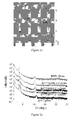
- Figure 1 is AFM topographic image of 2.5 nm BPTT:BPPh solid solution inducing layer with different component proportion, of all the component proportion in the experiment the solid solution films present layer by layer growth, adjacent domains coalesced, forming a large grain-sized, continuous and smooth thin films which is benefit for the epitaxial growth of upper semiconductor layer.
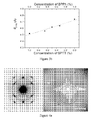
- Figure 2a is an out-of-plane X-ray diffraction patterns of 20 nm BPTT:BPPh films with different proportion.
- the patterns contain a series of (00/) diffraction, which means the thin film is highly ordered. Meanwhile, each diffraction peak shows a single peak, indicating the co-deposited thin films are of uniform composition with single-crystal-like structure, which is a solid solution thin film.
- Figure 2b indicated the diffraction peak continuously changes with component proportion.
- Figure 3 is in-plane X ray diffraction patterns of 20 nm BPTT:BPPh thin films of different proportion, all co-deposition films show a series diffraction peaks with single structure, and the thin film structure parameter thereof linearly varies with component proportion.
- Figure 4a and 4b are the selected area electron diffraction patterns of BPTT:BPPh (1:2) and (2:1)solid solution films, single domain shows diffraction pattern similar to that of single crystal, which further shows the co-deposition thin film is a solid solution film with a structure different from that of single component thin film.
- Figure 5 is the HOMO energy level of solid solution films with different component proportion, the HOMO value is between that of the two single substance films and varies with component proportion.
- Figure 6 is AFM topographic image of V0Pc thin film epitaxial grown on the inducing layer of BPTT:BPPh solid solution with component proportion of (2:1), (1:1), (1:2).
- V0Pc grows in the way of layer plus island.
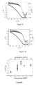
- Figure 7a shows a transistor configuration using the epitaxial V0Pc thin films as organic semiconductor layer.
- Figure 7b, c, d are the corresponding transistor transfer curves, which show the thin film presents high mobility.
- Figure 8a shows the relationship between the transistor mobility and component proportion of solid solution inducing layer, the thin film mobility acquires maximum value at the ratio of nearly (1:1).
- Figure 8b is relationship between threshold voltage and component proportion.
- the experiment method is the same as EXAMPLE 1, and the inducing layer material are P4T, F2-P4T.
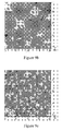
- Figure 9 is AFM topographic image of 2.5 nm P4T: F2 - P4T films with different component proportion. Thin film exhibit layer by layer growth mode, adjacent domains show a good coalescence, forming large grain-sized and smooth thin film. It is suitable for epitaxy growth as inducing layer.
- Figure 10 is in-plane XRD diffraction patterns of aforesaid co-deposition thin film. Thin film of all the component proportion shows almost the same lattice spacing. It is because the unit cell parameters of P4T and F2 - P4T are very approximate.
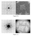
- Figure 11 shows the selected area electron diffraction patterns of the co-deposition thin films with component proportion respectively being (2:1), (1:1), (1:2), and each single domain of the thin films shows single-crystal-like diffraction pattern.
- Figure 12a is a diagram of the relation between the transistor mobility of V0Pc thin-film and the component proportion of the inducing layer. Its mobility linearly increases with the inducing layer component proportion.
- Figure 11 shows the change of threshold voltage with the proportion, similarly, it shows a trend that it varies with the component proportion of inducing layer linearly.
- the experiment method is the same as EXAMPLE 1, and the inducing layer materials are F2-BP3T, F4-BP3T.
- Figure 13 is an AFM topographic image of 2.5 nm co-deposition F2-BP3T : F4 - BP3T thin film (component ratio is 1:1).
- Figure 14 shows the device performance of the transistor based on V0Pc thin film epitaxial grown on aforesaid thin film.
- Table 1 shows solid solution inducing layer thin film co-deposited from different materials and the transisitor performance based on non-planar phthalocyanine thin film epitaxially grown on the corresponding solid solution inducing layer.
- the present invention is not limited to the above-mentioned embodiments.
- the inducing layer materials for the Weak Epitaxy Growth disclosed in the present invention can be used in other organic semiconductor components to prepare the components in two-dimensional or three-dimensional integrated device. These integrated devices can be applied in integrated circuits, active matrix display, sensors and photovoltaic cells.
- the electronic components based on the present invention are easy to be manufactured in large scale.
Landscapes
- Chemical & Material Sciences (AREA)
- Engineering & Computer Science (AREA)
- Materials Engineering (AREA)
- Organic Chemistry (AREA)
- Metallurgy (AREA)
- Chemical Kinetics & Catalysis (AREA)
- Crystallography & Structural Chemistry (AREA)
- Mechanical Engineering (AREA)
- Physics & Mathematics (AREA)
- Spectroscopy & Molecular Physics (AREA)
- Inorganic Chemistry (AREA)
- Thin Film Transistor (AREA)
- Electroluminescent Light Sources (AREA)
- Heterocyclic Carbon Compounds Containing A Hetero Ring Having Oxygen Or Sulfur (AREA)
Claims (10)
- Mischkristall-Induzierungsschicht für die schwachen epitaktischen Filme von nicht-planarem Phthalocyanin, dadurch gekennzeichnet, dass die Mischkristall-Induzierungsschicht durch zwei koabgeschiedene Induzierungsschichtmoleküle unter einer bestimmten Substrattemperatur gebildet wird, wobei der Mischkristall-Induzierungsschicht-Dünnfilm einheitlich ausgebildet ist und die Domänen eine einkristallartige Struktur aufweisen;
wobei die beiden Induzierungsschichtmoleküle Moleküle unterschiedlichen Typs sind und sich jeder der beiden Typen von Induzierungsschichtmolekülen durch eine der folgenden Strukturformeln darstellen lässt:


- Mischkristall-Induzierungsschicht für die schwachen epitaktischen Filme von nicht-planarem Phthalocyanin nach Anspruch 1, dadurch gekennzeichnet, dass Ar in Formel I eine der folgenden Strukturen enthält:


- Mischkristall-Induzierungsschicht für die schwachen epitaktischen Filme von nicht-planarem Phthalocyanin nach Anspruch 1, dadurch gekennzeichnet, dass die beiden Induzierungsschichtmoleküle nach einem der folgenden Typen kombiniert werden:Typ 1, der dadurch definiert ist, dass die beiden Moleküle als Endgruppen jeweils Phenylgruppen besitzen und sich die mittleren konjugierten aromatischen Gruppen zwischen den Endgruppen der beiden Moleküle voneinander unterscheiden;Typ 2, der dadurch definiert ist, dass ein Molekül der beiden Moleküle als Endgruppen Phenylgruppen und das andere Fluor-substituierte Phenylgruppen besitzt und die mittleren konjugierten aromatischen Gruppen zwischen den Endgruppen der beiden Moleküle gleich sind oder sich voneinander unterscheiden;Typ 3, der dadurch definiert ist, dass die beiden Moleküle als Endgruppen jeweils Fluor-substituierte Phenylgruppen besitzen und die mittleren konjugierten aromatischen Gruppen zwischen den Endgruppen der beiden Moleküle gleich sind oder sich voneinander unterscheiden.
- Mischkristall-Induzierungsschicht für die schwachen epitaktischen Filme von nicht-planarem Phthalocyanin nach Anspruch 1 oder 2, dadurch gekennzeichnet, dass die Substrattemperatur zwischen 150 °C und 240 °C liegt.
- Mischkristall-Induzierungsschicht für die schwachen epitaktischen Filme von nicht-planarem Phthalocyanin nach einem beliebigen der Ansprüche 1 bis 3, dadurch gekennzeichnet, dass bei der Koabscheidung die beiden Moleküle der Induzierungsschicht gleichzeitig durch Dampfabscheidung abgeschieden werden.
- Mischkristall-Induzierungsschicht für die schwachen epitaktischen Filme von nicht-planarem Phthalocyanin nach Anspruch 5, dadurch gekennzeichnet, dass es sich bei der Dampfabscheidung um molekulare Dampfabscheidung handelt, wobei das Vakuumniveau zwisehen 10-4 und 10-5 Pa liegt.
- Mischkristall-Induzierungsschicht für die schwachen epitaktischen Filme von nicht-planarem Phthalocyanin nach einem beliebigen der Ansprüche 1 bis 5, dadurch gekennzeichnet, dass vor der Koabscheidung der Induzierungsschichtmoleküle eine Siliziumnitridschicht auf dem Substrat abgeschieden wird, die eine Dicke von 200 bis 500 nm besitzt.
- Mischkristall-Induzierungsschicht für die schwachen epitaktischen Filme von nicht-planarem Phthalocyanin nach einem beliebigen der Ansprüche 1 bis 6, dadurch gekennzeichnet, dass die Dicke der Koabscheidungs-Mischkristall-Induzierungsschicht auf dem Substrat 1 bis 3 Molekularschichten beträgt.
- Dünnfilm aus nicht-planarem Phthalocyanin, dadurch gekennzeichnet, dass dieser durch das schwache epitaktische Wachstum des nicht-planaren Phthalocyanins auf einer beliebigen der Mischkristall-Induzierungsschichten nach den Ansprüchen 1 bis 7 gebildet wird und eine Orientierungsbeziehung zwischen dem Dünnfilm und der Mischkristall-Induzierungsschicht besteht.
- Organischer Dünnfilmtransistor, dadurch gekennzeichnet, dass dieser den Dünnfilm aus dem schwachen epitaktischen Wachstum des nicht-planaren Phthalocyanins auf der Mischkristall-Induzierungsschicht (3) nach Anspruch 9 enthält und dass es sich bei dem Dünnfilm aus dem schwachen epitaktischen Wachstum des nicht-planaren Phthalocyanins auf der Mischkristall-Induzierungsschicht um die organische Halbleiterschicht (2) im Transistor handelt.
Applications Claiming Priority (1)
| Application Number | Priority Date | Filing Date | Title |
|---|---|---|---|
| CN201010605569.2A CN102560632B (zh) | 2010-12-21 | 2010-12-21 | 用于非平面酞菁薄膜弱外延生长的固熔体诱导层 |
Publications (4)
| Publication Number | Publication Date |
|---|---|
| EP2468930A2 EP2468930A2 (de) | 2012-06-27 |
| EP2468930A9 EP2468930A9 (de) | 2012-08-22 |
| EP2468930A3 EP2468930A3 (de) | 2014-01-01 |
| EP2468930B1 true EP2468930B1 (de) | 2016-11-23 |
Family
ID=44674137
Family Applications (1)
| Application Number | Title | Priority Date | Filing Date |
|---|---|---|---|
| EP11171083.6A Not-in-force EP2468930B1 (de) | 2010-12-21 | 2011-06-22 | Feste Lösung zum Induzieren einer Schicht für schwaches Epitaxie-Wachstum (WEG) von nicht-planarem Phthalocyanin |
Country Status (4)
| Country | Link |
|---|---|
| US (1) | US8598151B2 (de) |
| EP (1) | EP2468930B1 (de) |
| JP (1) | JP5743848B2 (de) |
| CN (1) | CN102560632B (de) |
Families Citing this family (1)
| Publication number | Priority date | Publication date | Assignee | Title |
|---|---|---|---|---|
| CN105336880B (zh) * | 2015-10-23 | 2017-09-12 | 长春工业大学 | 一种基于双层诱导技术制备红荧烯薄膜的方法 |
Family Cites Families (7)
| Publication number | Priority date | Publication date | Assignee | Title |
|---|---|---|---|---|
| JP3664069B2 (ja) * | 1999-12-24 | 2005-06-22 | 松下電器産業株式会社 | 有機電界発光素子 |
| JP2003017276A (ja) * | 2001-04-27 | 2003-01-17 | Semiconductor Energy Lab Co Ltd | 発光装置及びその作製方法 |
| JP3946484B2 (ja) * | 2001-10-22 | 2007-07-18 | 独立行政法人科学技術振興機構 | 光電流増倍装置及びその増倍率制御方法 |
| US6869821B2 (en) * | 2002-12-30 | 2005-03-22 | Xerox Corporation | Method for producing organic electronic devices on deposited dielectric materials |
| JP4220951B2 (ja) * | 2004-09-24 | 2009-02-04 | 国立大学法人広島大学 | 新規な有機半導体化合物、その製造方法およびそれを用いた有機半導体デバイス |
| US7671448B2 (en) * | 2005-03-24 | 2010-03-02 | Semiconductor Energy Laboratory Co., Ltd. | Semiconductor device including two organic semiconductor layers |
| CN100555702C (zh) * | 2006-04-29 | 2009-10-28 | 中国科学院长春应用化学研究所 | 有机半导体晶体薄膜及弱取向外延生长制备方法和应用 |
-
2010
- 2010-12-21 CN CN201010605569.2A patent/CN102560632B/zh not_active Expired - Fee Related
-
2011
- 2011-06-22 EP EP11171083.6A patent/EP2468930B1/de not_active Not-in-force
- 2011-07-20 US US13/187,217 patent/US8598151B2/en not_active Expired - Fee Related
- 2011-10-27 JP JP2011235585A patent/JP5743848B2/ja not_active Expired - Fee Related
Non-Patent Citations (1)
| Title |
|---|
| None * |
Also Published As
| Publication number | Publication date |
|---|---|
| CN102560632B (zh) | 2016-06-29 |
| EP2468930A9 (de) | 2012-08-22 |
| JP2012134457A (ja) | 2012-07-12 |
| EP2468930A2 (de) | 2012-06-27 |
| US8598151B2 (en) | 2013-12-03 |
| JP5743848B2 (ja) | 2015-07-01 |
| US20120153265A1 (en) | 2012-06-21 |
| CN102560632A (zh) | 2012-07-11 |
| EP2468930A3 (de) | 2014-01-01 |
Similar Documents
| Publication | Publication Date | Title |
|---|---|---|
| US6734038B2 (en) | Method of manufacturing high-mobility organic thin films using organic vapor phase deposition | |
| Jiang et al. | High‐performance organic single‐crystal transistors and digital inverters of an anthracene derivative | |
| Kim et al. | Solvent-dependent electrical characteristics and stability of organic thin-film transistors with drop cast bis (triisopropylsilylethynyl) pentacene | |
| Wu et al. | Organic–inorganic hybrid CH 3 NH 3 PbI 3 perovskite materials as channels in thin-film field-effect transistors | |
| EP2190007B1 (de) | Monokristalldünnschicht einer organischen halbleiterverbindung und herstellungsverfahren dafür | |
| Kaji et al. | Co‐evaporant Induced Crystalline Donor: Acceptor Blends in Organic Solar Cells | |
| CN107109697B (zh) | 在衬底表面外延生长超薄有机晶体层的方法及其应用 | |
| JP2014505750A (ja) | 半導体ブレンド | |
| CN100555702C (zh) | 有机半导体晶体薄膜及弱取向外延生长制备方法和应用 | |
| CN102110776A (zh) | 一种高性能有机场效应晶体管及其制备方法 | |
| Tian et al. | An asymmetric oligomer based on thienoacene for solution processed crystal organic thin-film transistors | |
| US8758508B2 (en) | Formation of a thin film of molecular organic semiconductor material | |
| CN113540352B (zh) | 溶液加工与真空蒸镀结合制备有机晶体薄膜的方法 | |
| EP2468930A2 (de) | Feste Lösung zur Induzierung einer Schicht für Weichkristallwachstum von nicht-planarem Phthalocyanin | |
| Schoonveld et al. | Morphology of quaterthiophene thin films in organic field effect transistors | |
| Huang et al. | Heteroepitaxy growth high performance films of perylene diimide derivatives | |
| Wang et al. | Picene thin films on metal surfaces: Impact of molecular shape on interfacial coupling | |
| Nagashima et al. | Organic field-effect transistors based on naphthyl end-capped divinylbenzene: Performance, stability and molecular packing | |
| WO2020171131A1 (ja) | 有機半導体デバイス、有機半導体単結晶膜の製造方法、及び有機半導体デバイスの製造方法 | |
| KR102615101B1 (ko) | 유기주석 화합물을 포함하는 용액공정용 조성물, 및 이를 이용한 박막의 제조방법 | |
| CN102208364B (zh) | 与卷对卷技术兼容的大面积有机薄膜晶体管列阵制备方法 | |
| Qiao et al. | High performance lead phthalocyanine films and its effect on the field-effect transistors | |
| Itaka et al. | Molecular beam epitaxy of highly oriented pentacene thin films on an atomically flat sapphire substrate | |
| Matsumoto et al. | Effect of organic buffer layer on performance of pentacene field-effect transistor fabricated on natural mica gate dielectric | |
| JP5395842B2 (ja) | 真空蒸着成膜方法、真空蒸着成膜システム、結晶性真空蒸着膜 |
Legal Events
| Date | Code | Title | Description |
|---|---|---|---|
| AK | Designated contracting states |
Kind code of ref document: A2 Designated state(s): AL AT BE BG CH CY CZ DE DK EE ES FI FR GB GR HR HU IE IS IT LI LT LU LV MC MK MT NL NO PL PT RO RS SE SI SK SM TR |
|
| AX | Request for extension of the european patent |
Extension state: BA ME |
|
| PUAI | Public reference made under article 153(3) epc to a published international application that has entered the european phase |
Free format text: ORIGINAL CODE: 0009012 |
|
| PUAL | Search report despatched |
Free format text: ORIGINAL CODE: 0009013 |
|
| AK | Designated contracting states |
Kind code of ref document: A3 Designated state(s): AL AT BE BG CH CY CZ DE DK EE ES FI FR GB GR HR HU IE IS IT LI LT LU LV MC MK MT NL NO PL PT RO RS SE SI SK SM TR |
|
| AX | Request for extension of the european patent |
Extension state: BA ME |
|
| RIC1 | Information provided on ipc code assigned before grant |
Ipc: C30B 29/54 20060101ALI20131127BHEP Ipc: H01L 51/00 20060101ALI20131127BHEP Ipc: C30B 7/00 20060101AFI20131127BHEP Ipc: C23C 14/12 20060101ALI20131127BHEP Ipc: H01L 51/05 20060101ALI20131127BHEP Ipc: C23C 14/24 20060101ALI20131127BHEP |
|
| RAP1 | Party data changed (applicant data changed or rights of an application transferred) |
Owner name: CHANGCHUN FLEXIBLE DISPLAY TECHNOLOGY CO., LTD. |
|
| 17P | Request for examination filed |
Effective date: 20140701 |
|
| RBV | Designated contracting states (corrected) |
Designated state(s): AL AT BE BG CH CY CZ DE DK EE ES FI FR GB GR HR HU IE IS IT LI LT LU LV MC MK MT NL NO PL PT RO RS SE SI SK SM TR |
|
| REG | Reference to a national code |
Ref country code: DE Ref legal event code: R079 Ref document number: 602011032628 Country of ref document: DE Free format text: PREVIOUS MAIN CLASS: C30B0007000000 Ipc: C30B0023060000 |
|
| RIC1 | Information provided on ipc code assigned before grant |
Ipc: C30B 23/00 20060101ALI20160217BHEP Ipc: C30B 29/04 20060101ALI20160217BHEP Ipc: H01L 51/05 20060101ALI20160217BHEP Ipc: H01L 51/00 20060101ALI20160217BHEP Ipc: C30B 29/54 20060101ALI20160217BHEP Ipc: C23C 14/24 20060101ALI20160217BHEP Ipc: C30B 23/06 20060101AFI20160217BHEP Ipc: C23C 14/12 20060101ALI20160217BHEP |
|
| GRAP | Despatch of communication of intention to grant a patent |
Free format text: ORIGINAL CODE: EPIDOSNIGR1 |
|
| INTG | Intention to grant announced |
Effective date: 20160405 |
|
| GRAS | Grant fee paid |
Free format text: ORIGINAL CODE: EPIDOSNIGR3 |
|
| GRAJ | Information related to disapproval of communication of intention to grant by the applicant or resumption of examination proceedings by the epo deleted |
Free format text: ORIGINAL CODE: EPIDOSDIGR1 |
|
| GRAL | Information related to payment of fee for publishing/printing deleted |
Free format text: ORIGINAL CODE: EPIDOSDIGR3 |
|
| GRAP | Despatch of communication of intention to grant a patent |
Free format text: ORIGINAL CODE: EPIDOSNIGR1 |
|
| INTC | Intention to grant announced (deleted) | ||
| GRAA | (expected) grant |
Free format text: ORIGINAL CODE: 0009210 |
|
| INTG | Intention to grant announced |
Effective date: 20160930 |
|
| AK | Designated contracting states |
Kind code of ref document: B1 Designated state(s): AL AT BE BG CH CY CZ DE DK EE ES FI FR GB GR HR HU IE IS IT LI LT LU LV MC MK MT NL NO PL PT RO RS SE SI SK SM TR |
|
| REG | Reference to a national code |
Ref country code: GB Ref legal event code: FG4D |
|
| REG | Reference to a national code |
Ref country code: CH Ref legal event code: EP |
|
| REG | Reference to a national code |
Ref country code: IE Ref legal event code: FG4D |
|
| REG | Reference to a national code |
Ref country code: AT Ref legal event code: REF Ref document number: 848012 Country of ref document: AT Kind code of ref document: T Effective date: 20161215 |
|
| REG | Reference to a national code |
Ref country code: DE Ref legal event code: R096 Ref document number: 602011032628 Country of ref document: DE |
|
| PG25 | Lapsed in a contracting state [announced via postgrant information from national office to epo] |
Ref country code: LV Free format text: LAPSE BECAUSE OF FAILURE TO SUBMIT A TRANSLATION OF THE DESCRIPTION OR TO PAY THE FEE WITHIN THE PRESCRIBED TIME-LIMIT Effective date: 20161123 |
|
| REG | Reference to a national code |
Ref country code: LT Ref legal event code: MG4D |
|
| REG | Reference to a national code |
Ref country code: NL Ref legal event code: MP Effective date: 20161123 |
|
| REG | Reference to a national code |
Ref country code: AT Ref legal event code: MK05 Ref document number: 848012 Country of ref document: AT Kind code of ref document: T Effective date: 20161123 |
|
| PG25 | Lapsed in a contracting state [announced via postgrant information from national office to epo] |
Ref country code: SE Free format text: LAPSE BECAUSE OF FAILURE TO SUBMIT A TRANSLATION OF THE DESCRIPTION OR TO PAY THE FEE WITHIN THE PRESCRIBED TIME-LIMIT Effective date: 20161123 Ref country code: NO Free format text: LAPSE BECAUSE OF FAILURE TO SUBMIT A TRANSLATION OF THE DESCRIPTION OR TO PAY THE FEE WITHIN THE PRESCRIBED TIME-LIMIT Effective date: 20170223 Ref country code: LT Free format text: LAPSE BECAUSE OF FAILURE TO SUBMIT A TRANSLATION OF THE DESCRIPTION OR TO PAY THE FEE WITHIN THE PRESCRIBED TIME-LIMIT Effective date: 20161123 Ref country code: GR Free format text: LAPSE BECAUSE OF FAILURE TO SUBMIT A TRANSLATION OF THE DESCRIPTION OR TO PAY THE FEE WITHIN THE PRESCRIBED TIME-LIMIT Effective date: 20170224 Ref country code: NL Free format text: LAPSE BECAUSE OF FAILURE TO SUBMIT A TRANSLATION OF THE DESCRIPTION OR TO PAY THE FEE WITHIN THE PRESCRIBED TIME-LIMIT Effective date: 20161123 |
|
| PG25 | Lapsed in a contracting state [announced via postgrant information from national office to epo] |
Ref country code: PT Free format text: LAPSE BECAUSE OF FAILURE TO SUBMIT A TRANSLATION OF THE DESCRIPTION OR TO PAY THE FEE WITHIN THE PRESCRIBED TIME-LIMIT Effective date: 20170323 Ref country code: HR Free format text: LAPSE BECAUSE OF FAILURE TO SUBMIT A TRANSLATION OF THE DESCRIPTION OR TO PAY THE FEE WITHIN THE PRESCRIBED TIME-LIMIT Effective date: 20161123 Ref country code: ES Free format text: LAPSE BECAUSE OF FAILURE TO SUBMIT A TRANSLATION OF THE DESCRIPTION OR TO PAY THE FEE WITHIN THE PRESCRIBED TIME-LIMIT Effective date: 20161123 Ref country code: PL Free format text: LAPSE BECAUSE OF FAILURE TO SUBMIT A TRANSLATION OF THE DESCRIPTION OR TO PAY THE FEE WITHIN THE PRESCRIBED TIME-LIMIT Effective date: 20161123 Ref country code: AT Free format text: LAPSE BECAUSE OF FAILURE TO SUBMIT A TRANSLATION OF THE DESCRIPTION OR TO PAY THE FEE WITHIN THE PRESCRIBED TIME-LIMIT Effective date: 20161123 Ref country code: RS Free format text: LAPSE BECAUSE OF FAILURE TO SUBMIT A TRANSLATION OF THE DESCRIPTION OR TO PAY THE FEE WITHIN THE PRESCRIBED TIME-LIMIT Effective date: 20161123 Ref country code: FI Free format text: LAPSE BECAUSE OF FAILURE TO SUBMIT A TRANSLATION OF THE DESCRIPTION OR TO PAY THE FEE WITHIN THE PRESCRIBED TIME-LIMIT Effective date: 20161123 |
|
| PG25 | Lapsed in a contracting state [announced via postgrant information from national office to epo] |
Ref country code: CZ Free format text: LAPSE BECAUSE OF FAILURE TO SUBMIT A TRANSLATION OF THE DESCRIPTION OR TO PAY THE FEE WITHIN THE PRESCRIBED TIME-LIMIT Effective date: 20161123 Ref country code: SK Free format text: LAPSE BECAUSE OF FAILURE TO SUBMIT A TRANSLATION OF THE DESCRIPTION OR TO PAY THE FEE WITHIN THE PRESCRIBED TIME-LIMIT Effective date: 20161123 Ref country code: DK Free format text: LAPSE BECAUSE OF FAILURE TO SUBMIT A TRANSLATION OF THE DESCRIPTION OR TO PAY THE FEE WITHIN THE PRESCRIBED TIME-LIMIT Effective date: 20161123 Ref country code: RO Free format text: LAPSE BECAUSE OF FAILURE TO SUBMIT A TRANSLATION OF THE DESCRIPTION OR TO PAY THE FEE WITHIN THE PRESCRIBED TIME-LIMIT Effective date: 20161123 Ref country code: EE Free format text: LAPSE BECAUSE OF FAILURE TO SUBMIT A TRANSLATION OF THE DESCRIPTION OR TO PAY THE FEE WITHIN THE PRESCRIBED TIME-LIMIT Effective date: 20161123 |
|
| REG | Reference to a national code |
Ref country code: DE Ref legal event code: R097 Ref document number: 602011032628 Country of ref document: DE |
|
| PG25 | Lapsed in a contracting state [announced via postgrant information from national office to epo] |
Ref country code: SM Free format text: LAPSE BECAUSE OF FAILURE TO SUBMIT A TRANSLATION OF THE DESCRIPTION OR TO PAY THE FEE WITHIN THE PRESCRIBED TIME-LIMIT Effective date: 20161123 Ref country code: BG Free format text: LAPSE BECAUSE OF FAILURE TO SUBMIT A TRANSLATION OF THE DESCRIPTION OR TO PAY THE FEE WITHIN THE PRESCRIBED TIME-LIMIT Effective date: 20170223 Ref country code: IT Free format text: LAPSE BECAUSE OF FAILURE TO SUBMIT A TRANSLATION OF THE DESCRIPTION OR TO PAY THE FEE WITHIN THE PRESCRIBED TIME-LIMIT Effective date: 20161123 Ref country code: BE Free format text: LAPSE BECAUSE OF FAILURE TO SUBMIT A TRANSLATION OF THE DESCRIPTION OR TO PAY THE FEE WITHIN THE PRESCRIBED TIME-LIMIT Effective date: 20161123 |
|
| PLBE | No opposition filed within time limit |
Free format text: ORIGINAL CODE: 0009261 |
|
| STAA | Information on the status of an ep patent application or granted ep patent |
Free format text: STATUS: NO OPPOSITION FILED WITHIN TIME LIMIT |
|
| 26N | No opposition filed |
Effective date: 20170824 |
|
| PG25 | Lapsed in a contracting state [announced via postgrant information from national office to epo] |
Ref country code: SI Free format text: LAPSE BECAUSE OF FAILURE TO SUBMIT A TRANSLATION OF THE DESCRIPTION OR TO PAY THE FEE WITHIN THE PRESCRIBED TIME-LIMIT Effective date: 20161123 |
|
| PG25 | Lapsed in a contracting state [announced via postgrant information from national office to epo] |
Ref country code: MC Free format text: LAPSE BECAUSE OF FAILURE TO SUBMIT A TRANSLATION OF THE DESCRIPTION OR TO PAY THE FEE WITHIN THE PRESCRIBED TIME-LIMIT Effective date: 20161123 |
|
| REG | Reference to a national code |
Ref country code: CH Ref legal event code: PL |
|
| REG | Reference to a national code |
Ref country code: IE Ref legal event code: MM4A |
|
| REG | Reference to a national code |
Ref country code: FR Ref legal event code: ST Effective date: 20180228 |
|
| PG25 | Lapsed in a contracting state [announced via postgrant information from national office to epo] |
Ref country code: LI Free format text: LAPSE BECAUSE OF NON-PAYMENT OF DUE FEES Effective date: 20170630 Ref country code: LU Free format text: LAPSE BECAUSE OF NON-PAYMENT OF DUE FEES Effective date: 20170622 Ref country code: CH Free format text: LAPSE BECAUSE OF NON-PAYMENT OF DUE FEES Effective date: 20170630 Ref country code: IE Free format text: LAPSE BECAUSE OF NON-PAYMENT OF DUE FEES Effective date: 20170622 |
|
| PG25 | Lapsed in a contracting state [announced via postgrant information from national office to epo] |
Ref country code: FR Free format text: LAPSE BECAUSE OF NON-PAYMENT OF DUE FEES Effective date: 20170630 |
|
| PG25 | Lapsed in a contracting state [announced via postgrant information from national office to epo] |
Ref country code: MT Free format text: LAPSE BECAUSE OF NON-PAYMENT OF DUE FEES Effective date: 20170622 |
|
| PG25 | Lapsed in a contracting state [announced via postgrant information from national office to epo] |
Ref country code: HU Free format text: LAPSE BECAUSE OF FAILURE TO SUBMIT A TRANSLATION OF THE DESCRIPTION OR TO PAY THE FEE WITHIN THE PRESCRIBED TIME-LIMIT; INVALID AB INITIO Effective date: 20110622 |
|
| PG25 | Lapsed in a contracting state [announced via postgrant information from national office to epo] |
Ref country code: CY Free format text: LAPSE BECAUSE OF NON-PAYMENT OF DUE FEES Effective date: 20161123 |
|
| PG25 | Lapsed in a contracting state [announced via postgrant information from national office to epo] |
Ref country code: MK Free format text: LAPSE BECAUSE OF FAILURE TO SUBMIT A TRANSLATION OF THE DESCRIPTION OR TO PAY THE FEE WITHIN THE PRESCRIBED TIME-LIMIT Effective date: 20161123 |
|
| PG25 | Lapsed in a contracting state [announced via postgrant information from national office to epo] |
Ref country code: TR Free format text: LAPSE BECAUSE OF FAILURE TO SUBMIT A TRANSLATION OF THE DESCRIPTION OR TO PAY THE FEE WITHIN THE PRESCRIBED TIME-LIMIT Effective date: 20161123 |
|
| PG25 | Lapsed in a contracting state [announced via postgrant information from national office to epo] |
Ref country code: AL Free format text: LAPSE BECAUSE OF FAILURE TO SUBMIT A TRANSLATION OF THE DESCRIPTION OR TO PAY THE FEE WITHIN THE PRESCRIBED TIME-LIMIT Effective date: 20161123 Ref country code: IS Free format text: LAPSE BECAUSE OF FAILURE TO SUBMIT A TRANSLATION OF THE DESCRIPTION OR TO PAY THE FEE WITHIN THE PRESCRIBED TIME-LIMIT Effective date: 20170323 |
|
| PGFP | Annual fee paid to national office [announced via postgrant information from national office to epo] |
Ref country code: GB Payment date: 20220625 Year of fee payment: 12 Ref country code: DE Payment date: 20220610 Year of fee payment: 12 |
|
| REG | Reference to a national code |
Ref country code: DE Ref legal event code: R119 Ref document number: 602011032628 Country of ref document: DE |
|
| GBPC | Gb: european patent ceased through non-payment of renewal fee |
Effective date: 20230622 |
|
| PG25 | Lapsed in a contracting state [announced via postgrant information from national office to epo] |
Ref country code: DE Free format text: LAPSE BECAUSE OF NON-PAYMENT OF DUE FEES Effective date: 20240103 Ref country code: GB Free format text: LAPSE BECAUSE OF NON-PAYMENT OF DUE FEES Effective date: 20230622 |