EP2467416B1 - Ultrahochtemperatur-kunststoffverpackung und herstellungsverfahren dafür - Google Patents
Ultrahochtemperatur-kunststoffverpackung und herstellungsverfahren dafür Download PDFInfo
- Publication number
- EP2467416B1 EP2467416B1 EP09848563.4A EP09848563A EP2467416B1 EP 2467416 B1 EP2467416 B1 EP 2467416B1 EP 09848563 A EP09848563 A EP 09848563A EP 2467416 B1 EP2467416 B1 EP 2467416B1
- Authority
- EP
- European Patent Office
- Prior art keywords
- temperature
- melting temperature
- polymer
- polymeric material
- polymerization
- Prior art date
- Legal status (The legal status is an assumption and is not a legal conclusion. Google has not performed a legal analysis and makes no representation as to the accuracy of the status listed.)
- Not-in-force
Links
Images


Classifications
-
- C—CHEMISTRY; METALLURGY
- C08—ORGANIC MACROMOLECULAR COMPOUNDS; THEIR PREPARATION OR CHEMICAL WORKING-UP; COMPOSITIONS BASED THEREON
- C08G—MACROMOLECULAR COMPOUNDS OBTAINED OTHERWISE THAN BY REACTIONS ONLY INVOLVING UNSATURATED CARBON-TO-CARBON BONDS
- C08G85/00—General processes for preparing compounds provided for in this subclass
- C08G85/004—Modification of polymers by chemical after-treatment
-
- C—CHEMISTRY; METALLURGY
- C08—ORGANIC MACROMOLECULAR COMPOUNDS; THEIR PREPARATION OR CHEMICAL WORKING-UP; COMPOSITIONS BASED THEREON
- C08G—MACROMOLECULAR COMPOUNDS OBTAINED OTHERWISE THAN BY REACTIONS ONLY INVOLVING UNSATURATED CARBON-TO-CARBON BONDS
- C08G85/00—General processes for preparing compounds provided for in this subclass
- C08G85/002—Post-polymerisation treatment
-
- H—ELECTRICITY
- H01—ELECTRIC ELEMENTS
- H01L—SEMICONDUCTOR DEVICES NOT COVERED BY CLASS H10
- H01L23/00—Details of semiconductor or other solid state devices
- H01L23/28—Encapsulations, e.g. encapsulating layers, coatings, e.g. for protection
- H01L23/29—Encapsulations, e.g. encapsulating layers, coatings, e.g. for protection characterised by the material, e.g. carbon
- H01L23/293—Organic, e.g. plastic
-
- H—ELECTRICITY
- H01—ELECTRIC ELEMENTS
- H01L—SEMICONDUCTOR DEVICES NOT COVERED BY CLASS H10
- H01L2224/00—Indexing scheme for arrangements for connecting or disconnecting semiconductor or solid-state bodies and methods related thereto as covered by H01L24/00
- H01L2224/01—Means for bonding being attached to, or being formed on, the surface to be connected, e.g. chip-to-package, die-attach, "first-level" interconnects; Manufacturing methods related thereto
- H01L2224/26—Layer connectors, e.g. plate connectors, solder or adhesive layers; Manufacturing methods related thereto
- H01L2224/31—Structure, shape, material or disposition of the layer connectors after the connecting process
- H01L2224/32—Structure, shape, material or disposition of the layer connectors after the connecting process of an individual layer connector
- H01L2224/321—Disposition
- H01L2224/32151—Disposition the layer connector connecting between a semiconductor or solid-state body and an item not being a semiconductor or solid-state body, e.g. chip-to-substrate, chip-to-passive
- H01L2224/32221—Disposition the layer connector connecting between a semiconductor or solid-state body and an item not being a semiconductor or solid-state body, e.g. chip-to-substrate, chip-to-passive the body and the item being stacked
- H01L2224/32245—Disposition the layer connector connecting between a semiconductor or solid-state body and an item not being a semiconductor or solid-state body, e.g. chip-to-substrate, chip-to-passive the body and the item being stacked the item being metallic
-
- H—ELECTRICITY
- H01—ELECTRIC ELEMENTS
- H01L—SEMICONDUCTOR DEVICES NOT COVERED BY CLASS H10
- H01L2224/00—Indexing scheme for arrangements for connecting or disconnecting semiconductor or solid-state bodies and methods related thereto as covered by H01L24/00
- H01L2224/01—Means for bonding being attached to, or being formed on, the surface to be connected, e.g. chip-to-package, die-attach, "first-level" interconnects; Manufacturing methods related thereto
- H01L2224/42—Wire connectors; Manufacturing methods related thereto
- H01L2224/47—Structure, shape, material or disposition of the wire connectors after the connecting process
- H01L2224/48—Structure, shape, material or disposition of the wire connectors after the connecting process of an individual wire connector
- H01L2224/481—Disposition
- H01L2224/48151—Connecting between a semiconductor or solid-state body and an item not being a semiconductor or solid-state body, e.g. chip-to-substrate, chip-to-passive
- H01L2224/48221—Connecting between a semiconductor or solid-state body and an item not being a semiconductor or solid-state body, e.g. chip-to-substrate, chip-to-passive the body and the item being stacked
- H01L2224/48245—Connecting between a semiconductor or solid-state body and an item not being a semiconductor or solid-state body, e.g. chip-to-substrate, chip-to-passive the body and the item being stacked the item being metallic
- H01L2224/48247—Connecting between a semiconductor or solid-state body and an item not being a semiconductor or solid-state body, e.g. chip-to-substrate, chip-to-passive the body and the item being stacked the item being metallic connecting the wire to a bond pad of the item
-
- H—ELECTRICITY
- H01—ELECTRIC ELEMENTS
- H01L—SEMICONDUCTOR DEVICES NOT COVERED BY CLASS H10
- H01L2224/00—Indexing scheme for arrangements for connecting or disconnecting semiconductor or solid-state bodies and methods related thereto as covered by H01L24/00
- H01L2224/73—Means for bonding being of different types provided for in two or more of groups H01L2224/10, H01L2224/18, H01L2224/26, H01L2224/34, H01L2224/42, H01L2224/50, H01L2224/63, H01L2224/71
- H01L2224/732—Location after the connecting process
- H01L2224/73251—Location after the connecting process on different surfaces
- H01L2224/73265—Layer and wire connectors
-
- H—ELECTRICITY
- H01—ELECTRIC ELEMENTS
- H01L—SEMICONDUCTOR DEVICES NOT COVERED BY CLASS H10
- H01L23/00—Details of semiconductor or other solid state devices
- H01L23/02—Containers; Seals
- H01L23/04—Containers; Seals characterised by the shape of the container or parts, e.g. caps, walls
- H01L23/043—Containers; Seals characterised by the shape of the container or parts, e.g. caps, walls the container being a hollow construction and having a conductive base as a mounting as well as a lead for the semiconductor body
- H01L23/047—Containers; Seals characterised by the shape of the container or parts, e.g. caps, walls the container being a hollow construction and having a conductive base as a mounting as well as a lead for the semiconductor body the other leads being parallel to the base
-
- H—ELECTRICITY
- H01—ELECTRIC ELEMENTS
- H01L—SEMICONDUCTOR DEVICES NOT COVERED BY CLASS H10
- H01L24/00—Arrangements for connecting or disconnecting semiconductor or solid-state bodies; Methods or apparatus related thereto
- H01L24/73—Means for bonding being of different types provided for in two or more of groups H01L24/10, H01L24/18, H01L24/26, H01L24/34, H01L24/42, H01L24/50, H01L24/63, H01L24/71
-
- H—ELECTRICITY
- H01—ELECTRIC ELEMENTS
- H01L—SEMICONDUCTOR DEVICES NOT COVERED BY CLASS H10
- H01L2924/00—Indexing scheme for arrangements or methods for connecting or disconnecting semiconductor or solid-state bodies as covered by H01L24/00
- H01L2924/10—Details of semiconductor or other solid state devices to be connected
- H01L2924/11—Device type
- H01L2924/14—Integrated circuits
Definitions
- the present invention relates to circuit packages for integrated circuits and, more particularly, to such circuit packages that include polymers having high melting temperatures.
- plastics such as liquid crystal polymers (LCPs)
- LCPs liquid crystal polymers
- plastic is heated during one or more manufacturing steps of a product or later, such as while the product is in use.
- many products are manufactured by an injection molding process, which includes heating plastic to soften it and injecting the softened plastic into a mold.
- the plastic takes on the shape of the mold and (ideally) retains that shape during subsequent manufacturing steps and throughout the useful life of the resulting product.
- Some manufacturing processes and products could be improved through the use of a plastic that has a higher melting temperature than that of conventional plastics.
- Other manufacturing processes and products would benefit from the use of a plastic whose melting temperature can be raised after the plastic has been molded into a shape, but before a subsequent step that involves a temperature higher than the plastic's original melting point.
- solder is used to attach a microelectronic device (a "die") to a metal or other heat-conductive component (such as a mounting "flange” or “leadframe”) to maximize heat transfer from the die to the metal component.
- a microelectronic device a "die”
- a metal or other heat-conductive component such as a mounting "flange” or “leadframe”
- the metal component is attached to a heat sink, which is cooled, such as by natural air convection, forced airflow (typically from a fan) or a circulating cooling liquid.
- solders including gold-tin (AuSn) and gold-silicon (AuSi), are used to attach the die to the metal component of the circuit package.
- the solder is heated to a temperature (such as between about 280°C and about 320°C for AuSn or between about 390°C and about 430°C for AuSi) that exceeds the melting temperatures of conventional plastics.
- a temperature such as between about 280°C and about 320°C for AuSn or between about 390°C and about 430°C for AuSi
- most conventional plastics melt below about 300°C, and most liquid crystal polymers melt at temperatures near 330°C or slightly higher. Consequently, conventional plastics, including conventional LCPs, cannot be used in circuit packages.
- manufacturers typically use a ceramic material.
- ceramics must be brazed to the other components of a circuit package. Brazing is a high-temperature (approximately 800°C) process, which creates mechanical problems, such as out-of-flatness, in the circuit packages. Furthermore, manufacturing processes that involve ceramics are expensive.
- plastic is relatively inexpensive, and some LCPs have superior dielectric properties and other characteristics that would be desirable in electronic circuit packages. Unfortunately, the relatively low melting points of conventional LCPs and other plastics have prevented their practical use in such packages.
- a plastic material having a high melting temperature and a method for making such a plastic material are disclosed.
- the plastic material includes a high molecular weight polymer.
- the method increases the molecular weight of a polymer by continuing or resuming polymerization of the plastic material after an initial polymerization phase is completed.
- the initial polymerization typically occurs in a liquid state and can result in an intermediate solid material (to the extent plastics, such as liquid crystal polymers, are "solid").
- the material produced by the initial polymerization (referred to herein as an "intermediate material”) has an initial melting temperature. After the initial polymerization, the intermediate material is heated and undergoes further ("secondary”) polymerization, thereby lengthening polymer chains in the material.
- the disclosed plastic material can be used to make packages for microelectronic circuits and other useful products.
- the material is injection molded to form a frame on a metal flange. After the frame hardens, it is heated as disclosed herein to undergo further polymerization and raise its melting temperature. Subsequently, a die can be attached to the flange using a solder, such as AuSi, without melting the frame.
- a polymer is a chemical compound formed by the union of many identical, relatively simple molecules arranged in repeating, linked units to form a long, regular pattern, typically a chain.
- the linked units in the polymer chain are commonly referred to as "monomer units.”
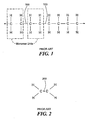
- Fig. 1 is a schematic diagram of an exemplary polymer (polyvinyl chloride). "Monomers” are the actual molecules used as the building blocks in the synthesis of a polymer.
- Fig. 2 is a schematic diagram the monomer (chloroethene) used to synthesize polyvinyl chloride.
- Several forms of polymerization are known, including addition polymerization, condensation polymerization and reactive polymerization.
- Heat a radical or another catalyst is often used during polymerization to alter the monomers.
- electrons and/or atoms of the monomers are rearranged to bond the monomers together to form the polymer chain. Because of the rearrangement of electrons and/or atoms, the linked monomer units in the polymer chain are not identical to the constituent monomers.
- the double bond 200 ( Fig. 2 ) between the carbon atoms of the monomer chloroethene is broken during polymerization, and one of the electron pairs from the double bond is used to bond the monomer units to each other, as shown at 100 ( Fig. 1 ).
- a liquid crystal is a material that exhibits some attributes of a liquid and other attributes of a solid.
- One common form of liquid crystal is a liquid crystal polymer (LCP), however not all liquid crystals are polymers.
- LCP liquid crystal polymer
- the molecules of materials forming liquid crystals are known as "mesogens."
- the mesogens of a liquid crystal can form ordered structures having long-range order, with the long axes of the mesogenic groups oriented in one preferred direction.
- the liquid-like properties of liquid crystals arise from the fact that these mesogenic structures can readily flow past one another.
- the solid-like properties arise because the structures themselves are not disturbed when the sliding occurs.
- a polymer is created, typically in a liquid form, from monomers, and after the polymeric chains are grown, the resulting material is typically cooled to a solid form.
- a polymer's molecular weight depends on the polymer's degree of polymerization, i.e., the lengths of the polymeric chains created.
- a monomer typically has a relatively small molecular weight, however a polymer typically includes up to millions of monomer units. Thus, polymers typically have high molecular weights. Properties, such as melting temperature, glass-transition temperature, heat deflection temperature and ductility, of a polymer are influenced by the polymer's molecular weight. However, all the molecules of a polymeric material typically do not have identical molecular weights. That is, during polymerization, some molecules grow longer than others. Because all the molecules of a polymeric material not necessarily have identical lengths, the material may not have a single, definite melting temperature. Instead, the material may gradually become softer as its temperature is raised over a relatively small range.
- the disclosed method operates after a traditional polymerization process. This is referred to herein as "secondary polymerization.”
- second polymerization the disclosed method can operate on solid polymeric materials, although the method can also operate on polymeric materials that are liquids or in other states.
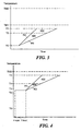
- a polymeric material with an initial melting temperature (TM1) is further (secondarily) polymerized to increase its melting temperature to TM2.
- the temperature of the material (after the traditional polymerization process) is increased from its initial temperature (T0) at a rate of between about 0.1 °C per hour (R1) and about 10°C per hour (R2) until the temperature of the material is between a first temperature (T1) about 10°C below the initial melting temperature and a second temperature (T2) about 30°C below the initial melting temperature of the material.
- T1 first temperature
- T2 a second temperature
- the temperature of the material is maintained for a minimum of about one hour, as shown in the graph of Fig. 4 . Then, the temperature of the material is increased at a rate of between about 0.1 °C per hour (R3) and about 10°C per hour (R4) until the temperature of the material is between a third temperature (T3) about 40°C below the desired new melting temperature and a fourth temperature (T4) about 50°C below the desired new melting temperature.
- the temperature of the material is raised, such that the material's time-temperature profile remains within region 400 and 402.
- the temperature of the material is increased to at least about 340°C. In other embodiments, the temperature is increased to at least about 355°C and 390°C, respectively.
- the highest temperature to which the material is raised during secondary polymerization is referred to herein as the "final temperature.”
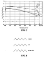
- Fig. 5 shows dynamic scanning calorimetry (DSC) plots of exemplary liquid crystal polymer materials made according to the disclosed method.
- DSC is a thermal analysis technique used to measure changes in heat flows associated with material transitions. DSC measurements provide both qualitative and quantitative data on endothermic (heat absorbing) and exothermic (heat evolving) processes. DSC is commonly used to determine the glass transition temperature and crystalline melting point of polymeric materials. A spike 500 in each plot shows the respective material's melting temperature. These melting temperatures exceed about 400°C, whereas the initial melting temperatures of the materials were between about 280°C and about 370°C.
- Exemplary original materials include those in a family of materials known as "aromatic polyesters” or liquid crystal polymers.
- ends of the original polymer chains contain one or more of the following groups: COOH, OH or acetic acid, as shown in Fig. 6 .
- some acid end (COOH) groups of the original polymer chains bond with acetate end groups of other polymer chains, and other acid end groups of the original polymer chains bond with residual OH ends on yet other polymer chains, resulting in very long chain polymers.
- a polyester monomer unit of the form 4-hydroxybenzoic acid (HBA) (or, more generally, p-hydrobenzoic acid), hydroquinone, bisphenol, tetrephthalic acid and/or 2-hydroxy-6-naphthoic acid is/are preferably present in the polymer chain. These monomer units are shown schematically in Fig. 7 .
- the secondary polymerization results in a cross-linked structure.
- An exemplary ultra-high molecular weight material that can be made according to the disclosed method is a liquid crystal polymer, i.e., a polymer containing HBA monomer units, that is heated during secondary polymerization to a final temperature of about 390°C.
- a liquid crystal polymer i.e., a polymer containing HBA monomer units
- Such a material has a melting temperature greater than about 420°C.
- exemplary material has a molecular weight greater than about 30,000 gm/mol.
- exemplary material has a tensile strength greater than about 172 369 kPA (25,000 psi).
- Another, similarly made, exemplary material has an elongation greater than about 2%.
- exemplary material includes more than about 200 repeating ester groups.
- Fig. 8 illustrates such a package 800.
- a flange 802 is made of a highly thermally conductive material, such as a high-copper alloy, or another suitable material.
- the flange 802 includes slots 804, by which the flange can later be mechanically attached, such as by bolts, to a heat sink (not shown).
- a dielectric frame 806 is made of a polymeric material before the disclosed secondary polymerization is performed on the polymeric material.
- the frame 806 is injection molded to the flange 802. Both the compounding temperature for the polymeric material and the molding temperature for the injection molding are less than the maximum temperature used in the subsequent secondary polymerization process.
- Figs. 9 and 10 are cut-away views of alternative embodiments of the circuit package 800 of Fig. 8 .
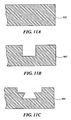
- the flange 802 optionally includes a concave keyway 900 ( Fig. 9 ) or a convex key 1000 ( Fig. 10 ), into which or around which the plastic material is injected during the injection molding process.
- the keyway 900 can be formed in the flange 802 by progressively stamping the flange 802 with a series of toolings, as shown in Fig. 11 (A-C).
- the key 1000 can be similarly formed. Because the polymeric material is injection molded to the flange 802 before the melting temperature of the material is raised, conventional temperatures, processes and equipment can be used for the injection molding process.
- the disclosed secondary polymerization process is performed, as discussed above, and the melting temperature of the plastic material of the frame 806 is increased, such that the end-use temperature of the plastic material is higher than the compounding and the molding temperatures.
- a die 808 ( Fig. 8 ) is attached by solder 810 to a die-attached area 812 of the flange 802. Because the melting temperature of the frame 806 has been increased, the frame 806 can withstand the temperatures encountered when the die 808 is soldered to the flange 802, without damage to the frame 806. Wires 814 electrically connect the die 808 to leads 816.
- a lid (not shown) is attached to the frame 806, such as by ultrasonic welding, by epoxy or by another suitable method.
- the flange 802, the frame 806 and the lid provide a hermetically sealed cavity for the die 808.
- the cavity can be evacuated or filled with air, an inert gas, epoxy or another appropriate material.
- the flange 802, the frame 806 and the lid prevent infiltration of moisture, gases and other contaminants into the cavity.
- circuit packages do not include a flange.
- the frame is molded to a leadframe, and the die is electrically (and sometimes mechanically and/or thermally) connected to the leadframe.
- the above-described method of secondary polymerization applies to such flangeless packages and other circuit packages.
- any metal or other material in a circuit package, to which a frame is molded is referred to hereinafter as a flange.
- the secondary polymerization process described with respect to circuit packages can be applied to other articles of manufacture that include components that are molded to other components.
- thermoplastic is a material that can be repeatedly softened by heating and hardened by cooling. Thus, a thermoplastic can be remoled by reheating the material.
- a thermoset plastic is a material that will undergo or has undergone a chemical reaction ("curing") by the action of heat, catalysts, ultra-violet light, etc., leading to a relatively infusible state. Once cured, a thermoset material cannot be returned to the uncured state. Thus, thermoset materials cannot be repeatedly softened or remolded.
- the methods disclosed herein are applicable to thermoplastic and thermoset materials.
- the frame of a circuit package can be made from a thermoplastic or from a thermoset material.
- the secondary polymerization process can be applied to already molded and frozen thermoplastic materials, resulting in a higher molecular weight thermoplastic that has a very high melting temperature.
- the secondary polymerization process can also be applied to a thermoset material, which no longer melts.
Landscapes
- Chemical & Material Sciences (AREA)
- Organic Chemistry (AREA)
- Chemical Kinetics & Catalysis (AREA)
- Medicinal Chemistry (AREA)
- Polymers & Plastics (AREA)
- Health & Medical Sciences (AREA)
- Power Engineering (AREA)
- Microelectronics & Electronic Packaging (AREA)
- Condensed Matter Physics & Semiconductors (AREA)
- General Physics & Mathematics (AREA)
- Computer Hardware Design (AREA)
- Engineering & Computer Science (AREA)
- Physics & Mathematics (AREA)
- General Chemical & Material Sciences (AREA)
- Polyesters Or Polycarbonates (AREA)
- Injection Moulding Of Plastics Or The Like (AREA)
- Processing And Handling Of Plastics And Other Materials For Molding In General (AREA)
- Treatments Of Macromolecular Shaped Articles (AREA)
- Encapsulation Of And Coatings For Semiconductor Or Solid State Devices (AREA)
Claims (10)
- Verfahren zur Erhöhung der Schmelztemperatur eines Polymermaterials, wobei das Verfahren dadurch gekennzeichnet ist, dass es umfasst:Spritzgießen eines ersten Polymermaterials in eine Form,Erhöhen der Temperatur des gegossenen Polymermaterials in gegossener Form mit einer ersten Geschwindigkeit von 0,1 °C pro Stunde bis 10°C pro Stunde, bis die Temperatur des Materials eine erste Temperatur zwischen 10°C und 30°C unter einer ursprünglichen Schmelztemperatur des Materials erreicht,Halten der Temperatur des Materials zwischen 10°C und 30°C unter der ursprünglichen Schmelztemperatur des Materials für die Dauer von wenigstens einer Stunde undErhöhen der Temperatur des Materials in gegossener Form mit einer Geschwindigkeit von 0,1 °C pro Stunde bis 10°C pro Stunde, bis die Temperatur des Materials eine zweite Temperatur zwischen 40°C und 50°C unter einer gewünschten Schmelztemperatur des Materials erreicht.
- Verfahren nach Anspruch 1, wobei die gewünschte Schmelztemperatur höher als 340°C, höher als 355°C, höher als 390°C, wenigstens 400°C oder wenigstens 420°C ist.
- Verfahren nach Anspruch 1, wobei das Polymermaterial ein Flüssigkristallpolymer ist.
- Verfahren nach Anspruch 1, wobei die gewünschte Schmelztemperatur wenigstens 100°C über der ursprünglichen Schmelztemperatur liegt.
- Verfahren nach Anspruch 1, wobei das Polymermaterial wenigstens eine Monomereinheit, die aus Hydrochinon, Bisphenol, Isophthalsäure, p-Hydroxybenzoesäure, Terephthalsäure und 2-Hydroxy-6-Naphthoesäure gewählt ist, umfasst.
- Verfahren nach Anspruch 1, wobei das Polymermaterial wenigstens eine Endgruppe, die aus -COOH, -OH und -CH2COOH gewählt ist, aufweist.
- Verfahren nach Anspruch 1, ferner umfassend den Schritt des Synthetisierens des Polymermaterials.
- Flüssigkristallpolymermaterial, das durch ein Verfahren nach einem der vorhergehenden Ansprüche hergestellt ist.
- Material nach Anspruch 8, das im Durchschnitt wenigstens 200 Monomereinheiten pro Polymer aufweist.
- Material nach Anspruch 8, das als Schaltkreisgehäuse ausgelegt ist.
Applications Claiming Priority (1)
| Application Number | Priority Date | Filing Date | Title |
|---|---|---|---|
| PCT/US2009/054451 WO2011022010A1 (en) | 2009-08-20 | 2009-08-20 | Ultra high-remperature plastic package and method of manufacture |
Publications (4)
| Publication Number | Publication Date |
|---|---|
| EP2467416A1 EP2467416A1 (de) | 2012-06-27 |
| EP2467416A4 EP2467416A4 (de) | 2013-03-27 |
| EP2467416B1 true EP2467416B1 (de) | 2015-03-25 |
| EP2467416B8 EP2467416B8 (de) | 2015-08-26 |
Family
ID=43607244
Family Applications (1)
| Application Number | Title | Priority Date | Filing Date |
|---|---|---|---|
| EP09848563.4A Not-in-force EP2467416B8 (de) | 2009-08-20 | 2009-08-20 | Ultrahochtemperatur-kunststoffverpackung und herstellungsverfahren dafür |
Country Status (4)
| Country | Link |
|---|---|
| EP (1) | EP2467416B8 (de) |
| JP (1) | JP5707404B2 (de) |
| CN (1) | CN102482428B (de) |
| WO (1) | WO2011022010A1 (de) |
Families Citing this family (1)
| Publication number | Priority date | Publication date | Assignee | Title |
|---|---|---|---|---|
| CN120555073A (zh) * | 2019-04-12 | 2025-08-29 | 佳胜科技股份有限公司 | 改质液晶高分子的制作方法及液晶高分子组合物 |
Family Cites Families (11)
| Publication number | Priority date | Publication date | Assignee | Title |
|---|---|---|---|---|
| US3718621A (en) * | 1969-09-17 | 1973-02-27 | Goodyear Tire & Rubber | Solid state polymerization process |
| US3890283A (en) * | 1973-06-04 | 1975-06-17 | American Cyanamid Co | Process for post-polymerizing polyglycolic acid |
| JPS63234030A (ja) * | 1987-03-23 | 1988-09-29 | Teijin Ltd | 熱硬化樹脂成形物 |
| JPH0757534B2 (ja) * | 1988-01-30 | 1995-06-21 | 日本エステル株式会社 | ポリエステル成形品の処理方法 |
| JP3087430B2 (ja) * | 1992-04-06 | 2000-09-11 | 住友化学工業株式会社 | 粉体状ポリマーの固相重合方法 |
| JP3655464B2 (ja) * | 1998-04-13 | 2005-06-02 | 株式会社クラレ | ポリマーフィルムとその製造方法並びに積層体 |
| JPH11291350A (ja) * | 1998-04-13 | 1999-10-26 | Kuraray Co Ltd | ポリマーフィルムとその製造方法 |
| JP3979995B2 (ja) * | 2001-05-15 | 2007-09-19 | 電気化学工業株式会社 | オレフィン−芳香族ビニル化合物共重合体の製造方法 |
| ES2391766T3 (es) * | 2002-09-20 | 2012-11-29 | Exxonmobil Chemical Patents Inc. | Producción de polímeros en condiciones supercríticas |
| US7014791B2 (en) * | 2002-12-18 | 2006-03-21 | E.I. Du Pont De Nemours And Company | Liquid crystalline polymer composition |
| SG157957A1 (en) * | 2003-01-29 | 2010-01-29 | Interplex Qlp Inc | Package for integrated circuit die |
-
2009
- 2009-08-20 EP EP09848563.4A patent/EP2467416B8/de not_active Not-in-force
- 2009-08-20 CN CN200980161021.9A patent/CN102482428B/zh active Active
- 2009-08-20 JP JP2012525517A patent/JP5707404B2/ja not_active Expired - Fee Related
- 2009-08-20 WO PCT/US2009/054451 patent/WO2011022010A1/en not_active Ceased
Also Published As
| Publication number | Publication date |
|---|---|
| EP2467416A1 (de) | 2012-06-27 |
| CN102482428A (zh) | 2012-05-30 |
| EP2467416B8 (de) | 2015-08-26 |
| JP5707404B2 (ja) | 2015-04-30 |
| CN102482428B (zh) | 2014-12-31 |
| WO2011022010A1 (en) | 2011-02-24 |
| WO2011022010A8 (en) | 2011-05-12 |
| JP2013502482A (ja) | 2013-01-24 |
| EP2467416A4 (de) | 2013-03-27 |
Similar Documents
| Publication | Publication Date | Title |
|---|---|---|
| US20100305279A1 (en) | Ultra high-temperature plastic package and method of manufacture | |
| US7868113B2 (en) | Low shrinkage polyester thermosetting resins | |
| TWI599469B (zh) | 液晶聚合物模製品及其製造方法 | |
| Ishak et al. | On the in‐situ polymerization of cyclic butylene terephthalate oligomers: DSC and rheological studies | |
| TWI555625B (zh) | 液晶聚合物模製物件 | |
| CN109824876A (zh) | 一种热致液晶聚合物及其制备方法与应用 | |
| CN102217108A (zh) | 具有由芳香族聚酯和/或全芳香性聚酯制成的反射件的功率led器件 | |
| CA2710098A1 (en) | Crystalline polyglycolic acid, polyglycolic acid composition and production process thereof | |
| CN113929901B (zh) | 一种聚酰胺树脂、其组合物及制备方法 | |
| KR101175972B1 (ko) | 액정 폴리에스테르 수지 및 이의 제조 방법 | |
| US20210024687A1 (en) | Aromatic liquid crystal polyester, aromatic liquid crystal polyester composition, and molded article | |
| EP2467416B1 (de) | Ultrahochtemperatur-kunststoffverpackung und herstellungsverfahren dafür | |
| CN109824875A (zh) | 一种液晶聚酯 | |
| TWI468446B (zh) | 超高溫塑膠封裝及製造方法 | |
| JP2020164738A (ja) | 液晶ポリエステル成形体及びコネクター | |
| US5767223A (en) | Wholly-aromatic thermotropic liquid crystal polyester and sealing material for electric and electronic parts | |
| US6326237B1 (en) | Reworkable thermoplastic hyper-branched encapsulant | |
| KR102394654B1 (ko) | 변성 액정 폴리머 제조방법, 액정 폴리머 조성물 및 액정 폴리머의 융점을 변경하기 위한 방법 | |
| Chien et al. | Low stress polymer die attach adhesive for plastic packages | |
| JP4306268B2 (ja) | 芳香族液晶ポリエステルおよびそのフィルム | |
| US20130308287A1 (en) | Power device and package for power device | |
| KR20150079071A (ko) | 전방향족 액정 폴리에스테르 섬유 및 이의 제조 방법 | |
| KR20200047353A (ko) | 폴리아릴렌 설파이드의 제조 방법 | |
| Fan et al. | Thermosetting and thermoplastic bisphenol A epoxy/phenoxy resin as encapsulant material | |
| Economy et al. | Solid state interchain transesterification reactions in macromolecules |
Legal Events
| Date | Code | Title | Description |
|---|---|---|---|
| PUAI | Public reference made under article 153(3) epc to a published international application that has entered the european phase |
Free format text: ORIGINAL CODE: 0009012 |
|
| 17P | Request for examination filed |
Effective date: 20120320 |
|
| AK | Designated contracting states |
Kind code of ref document: A1 Designated state(s): AT BE BG CH CY CZ DE DK EE ES FI FR GB GR HR HU IE IS IT LI LT LU LV MC MK MT NL NO PL PT RO SE SI SK SM TR |
|
| DAX | Request for extension of the european patent (deleted) | ||
| A4 | Supplementary search report drawn up and despatched |
Effective date: 20130221 |
|
| RIC1 | Information provided on ipc code assigned before grant |
Ipc: C08G 85/00 20060101AFI20130215BHEP |
|
| 17Q | First examination report despatched |
Effective date: 20131104 |
|
| GRAP | Despatch of communication of intention to grant a patent |
Free format text: ORIGINAL CODE: EPIDOSNIGR1 |
|
| INTG | Intention to grant announced |
Effective date: 20140331 |
|
| GRAS | Grant fee paid |
Free format text: ORIGINAL CODE: EPIDOSNIGR3 |
|
| RAP1 | Party data changed (applicant data changed or rights of an application transferred) |
Owner name: IQLP, LLC |
|
| GRAA | (expected) grant |
Free format text: ORIGINAL CODE: 0009210 |
|
| AK | Designated contracting states |
Kind code of ref document: B1 Designated state(s): AT BE BG CH CY CZ DE DK EE ES FI FR GB GR HR HU IE IS IT LI LT LU LV MC MK MT NL NO PL PT RO SE SI SK SM TR |
|
| REG | Reference to a national code |
Ref country code: GB Ref legal event code: FG4D |
|
| REG | Reference to a national code |
Ref country code: CH Ref legal event code: EP |
|
| REG | Reference to a national code |
Ref country code: IE Ref legal event code: FG4D |
|
| REG | Reference to a national code |
Ref country code: DE Ref legal event code: R096 Ref document number: 602009030273 Country of ref document: DE Effective date: 20150507 |
|
| REG | Reference to a national code |
Ref country code: AT Ref legal event code: REF Ref document number: 717856 Country of ref document: AT Kind code of ref document: T Effective date: 20150515 |
|
| PG25 | Lapsed in a contracting state [announced via postgrant information from national office to epo] |
Ref country code: LT Free format text: LAPSE BECAUSE OF FAILURE TO SUBMIT A TRANSLATION OF THE DESCRIPTION OR TO PAY THE FEE WITHIN THE PRESCRIBED TIME-LIMIT Effective date: 20150325 Ref country code: NO Free format text: LAPSE BECAUSE OF FAILURE TO SUBMIT A TRANSLATION OF THE DESCRIPTION OR TO PAY THE FEE WITHIN THE PRESCRIBED TIME-LIMIT Effective date: 20150625 Ref country code: FI Free format text: LAPSE BECAUSE OF FAILURE TO SUBMIT A TRANSLATION OF THE DESCRIPTION OR TO PAY THE FEE WITHIN THE PRESCRIBED TIME-LIMIT Effective date: 20150325 Ref country code: HR Free format text: LAPSE BECAUSE OF FAILURE TO SUBMIT A TRANSLATION OF THE DESCRIPTION OR TO PAY THE FEE WITHIN THE PRESCRIBED TIME-LIMIT Effective date: 20150325 Ref country code: SE Free format text: LAPSE BECAUSE OF FAILURE TO SUBMIT A TRANSLATION OF THE DESCRIPTION OR TO PAY THE FEE WITHIN THE PRESCRIBED TIME-LIMIT Effective date: 20150325 |
|
| REG | Reference to a national code |
Ref country code: AT Ref legal event code: MK05 Ref document number: 717856 Country of ref document: AT Kind code of ref document: T Effective date: 20150325 |
|
| REG | Reference to a national code |
Ref country code: LT Ref legal event code: MG4D |
|
| PG25 | Lapsed in a contracting state [announced via postgrant information from national office to epo] |
Ref country code: LV Free format text: LAPSE BECAUSE OF FAILURE TO SUBMIT A TRANSLATION OF THE DESCRIPTION OR TO PAY THE FEE WITHIN THE PRESCRIBED TIME-LIMIT Effective date: 20150325 Ref country code: GR Free format text: LAPSE BECAUSE OF FAILURE TO SUBMIT A TRANSLATION OF THE DESCRIPTION OR TO PAY THE FEE WITHIN THE PRESCRIBED TIME-LIMIT Effective date: 20150626 |
|
| PGFP | Annual fee paid to national office [announced via postgrant information from national office to epo] |
Ref country code: IE Payment date: 20150619 Year of fee payment: 7 |
|
| PG25 | Lapsed in a contracting state [announced via postgrant information from national office to epo] |
Ref country code: NL Free format text: LAPSE BECAUSE OF FAILURE TO SUBMIT A TRANSLATION OF THE DESCRIPTION OR TO PAY THE FEE WITHIN THE PRESCRIBED TIME-LIMIT Effective date: 20150325 |
|
| PG25 | Lapsed in a contracting state [announced via postgrant information from national office to epo] |
Ref country code: ES Free format text: LAPSE BECAUSE OF FAILURE TO SUBMIT A TRANSLATION OF THE DESCRIPTION OR TO PAY THE FEE WITHIN THE PRESCRIBED TIME-LIMIT Effective date: 20150325 Ref country code: EE Free format text: LAPSE BECAUSE OF FAILURE TO SUBMIT A TRANSLATION OF THE DESCRIPTION OR TO PAY THE FEE WITHIN THE PRESCRIBED TIME-LIMIT Effective date: 20150325 Ref country code: SK Free format text: LAPSE BECAUSE OF FAILURE TO SUBMIT A TRANSLATION OF THE DESCRIPTION OR TO PAY THE FEE WITHIN THE PRESCRIBED TIME-LIMIT Effective date: 20150325 Ref country code: PT Free format text: LAPSE BECAUSE OF FAILURE TO SUBMIT A TRANSLATION OF THE DESCRIPTION OR TO PAY THE FEE WITHIN THE PRESCRIBED TIME-LIMIT Effective date: 20150829 Ref country code: CZ Free format text: LAPSE BECAUSE OF FAILURE TO SUBMIT A TRANSLATION OF THE DESCRIPTION OR TO PAY THE FEE WITHIN THE PRESCRIBED TIME-LIMIT Effective date: 20150325 Ref country code: RO Free format text: LAPSE BECAUSE OF FAILURE TO SUBMIT A TRANSLATION OF THE DESCRIPTION OR TO PAY THE FEE WITHIN THE PRESCRIBED TIME-LIMIT Effective date: 20150325 |
|
| PG25 | Lapsed in a contracting state [announced via postgrant information from national office to epo] |
Ref country code: AT Free format text: LAPSE BECAUSE OF FAILURE TO SUBMIT A TRANSLATION OF THE DESCRIPTION OR TO PAY THE FEE WITHIN THE PRESCRIBED TIME-LIMIT Effective date: 20150325 Ref country code: IS Free format text: LAPSE BECAUSE OF FAILURE TO SUBMIT A TRANSLATION OF THE DESCRIPTION OR TO PAY THE FEE WITHIN THE PRESCRIBED TIME-LIMIT Effective date: 20150725 Ref country code: PL Free format text: LAPSE BECAUSE OF FAILURE TO SUBMIT A TRANSLATION OF THE DESCRIPTION OR TO PAY THE FEE WITHIN THE PRESCRIBED TIME-LIMIT Effective date: 20150325 |
|
| REG | Reference to a national code |
Ref country code: DE Ref legal event code: R097 Ref document number: 602009030273 Country of ref document: DE |
|
| PG25 | Lapsed in a contracting state [announced via postgrant information from national office to epo] |
Ref country code: DK Free format text: LAPSE BECAUSE OF FAILURE TO SUBMIT A TRANSLATION OF THE DESCRIPTION OR TO PAY THE FEE WITHIN THE PRESCRIBED TIME-LIMIT Effective date: 20150325 |
|
| PLBE | No opposition filed within time limit |
Free format text: ORIGINAL CODE: 0009261 |
|
| STAA | Information on the status of an ep patent application or granted ep patent |
Free format text: STATUS: NO OPPOSITION FILED WITHIN TIME LIMIT |
|
| 26N | No opposition filed |
Effective date: 20160105 |
|
| PG25 | Lapsed in a contracting state [announced via postgrant information from national office to epo] |
Ref country code: LU Free format text: LAPSE BECAUSE OF FAILURE TO SUBMIT A TRANSLATION OF THE DESCRIPTION OR TO PAY THE FEE WITHIN THE PRESCRIBED TIME-LIMIT Effective date: 20150820 Ref country code: MC Free format text: LAPSE BECAUSE OF FAILURE TO SUBMIT A TRANSLATION OF THE DESCRIPTION OR TO PAY THE FEE WITHIN THE PRESCRIBED TIME-LIMIT Effective date: 20150325 |
|
| REG | Reference to a national code |
Ref country code: CH Ref legal event code: PL |
|
| GBPC | Gb: european patent ceased through non-payment of renewal fee |
Effective date: 20150820 |
|
| PG25 | Lapsed in a contracting state [announced via postgrant information from national office to epo] |
Ref country code: LI Free format text: LAPSE BECAUSE OF NON-PAYMENT OF DUE FEES Effective date: 20150831 Ref country code: IT Free format text: LAPSE BECAUSE OF FAILURE TO SUBMIT A TRANSLATION OF THE DESCRIPTION OR TO PAY THE FEE WITHIN THE PRESCRIBED TIME-LIMIT Effective date: 20150325 Ref country code: CH Free format text: LAPSE BECAUSE OF NON-PAYMENT OF DUE FEES Effective date: 20150831 |
|
| PG25 | Lapsed in a contracting state [announced via postgrant information from national office to epo] |
Ref country code: SI Free format text: LAPSE BECAUSE OF FAILURE TO SUBMIT A TRANSLATION OF THE DESCRIPTION OR TO PAY THE FEE WITHIN THE PRESCRIBED TIME-LIMIT Effective date: 20150325 |
|
| REG | Reference to a national code |
Ref country code: FR Ref legal event code: ST Effective date: 20160429 |
|
| PG25 | Lapsed in a contracting state [announced via postgrant information from national office to epo] |
Ref country code: GB Free format text: LAPSE BECAUSE OF NON-PAYMENT OF DUE FEES Effective date: 20150820 |
|
| PG25 | Lapsed in a contracting state [announced via postgrant information from national office to epo] |
Ref country code: BE Free format text: LAPSE BECAUSE OF FAILURE TO SUBMIT A TRANSLATION OF THE DESCRIPTION OR TO PAY THE FEE WITHIN THE PRESCRIBED TIME-LIMIT Effective date: 20150325 Ref country code: FR Free format text: LAPSE BECAUSE OF NON-PAYMENT OF DUE FEES Effective date: 20150831 |
|
| PG25 | Lapsed in a contracting state [announced via postgrant information from national office to epo] |
Ref country code: MT Free format text: LAPSE BECAUSE OF FAILURE TO SUBMIT A TRANSLATION OF THE DESCRIPTION OR TO PAY THE FEE WITHIN THE PRESCRIBED TIME-LIMIT Effective date: 20150325 |
|
| PG25 | Lapsed in a contracting state [announced via postgrant information from national office to epo] |
Ref country code: SM Free format text: LAPSE BECAUSE OF FAILURE TO SUBMIT A TRANSLATION OF THE DESCRIPTION OR TO PAY THE FEE WITHIN THE PRESCRIBED TIME-LIMIT Effective date: 20150325 Ref country code: HU Free format text: LAPSE BECAUSE OF FAILURE TO SUBMIT A TRANSLATION OF THE DESCRIPTION OR TO PAY THE FEE WITHIN THE PRESCRIBED TIME-LIMIT; INVALID AB INITIO Effective date: 20090820 Ref country code: BG Free format text: LAPSE BECAUSE OF FAILURE TO SUBMIT A TRANSLATION OF THE DESCRIPTION OR TO PAY THE FEE WITHIN THE PRESCRIBED TIME-LIMIT Effective date: 20150325 |
|
| REG | Reference to a national code |
Ref country code: IE Ref legal event code: MM4A |
|
| PG25 | Lapsed in a contracting state [announced via postgrant information from national office to epo] |
Ref country code: CY Free format text: LAPSE BECAUSE OF FAILURE TO SUBMIT A TRANSLATION OF THE DESCRIPTION OR TO PAY THE FEE WITHIN THE PRESCRIBED TIME-LIMIT Effective date: 20150325 |
|
| PG25 | Lapsed in a contracting state [announced via postgrant information from national office to epo] |
Ref country code: IE Free format text: LAPSE BECAUSE OF NON-PAYMENT OF DUE FEES Effective date: 20160820 |
|
| PG25 | Lapsed in a contracting state [announced via postgrant information from national office to epo] |
Ref country code: TR Free format text: LAPSE BECAUSE OF FAILURE TO SUBMIT A TRANSLATION OF THE DESCRIPTION OR TO PAY THE FEE WITHIN THE PRESCRIBED TIME-LIMIT Effective date: 20150325 |
|
| PG25 | Lapsed in a contracting state [announced via postgrant information from national office to epo] |
Ref country code: MK Free format text: LAPSE BECAUSE OF FAILURE TO SUBMIT A TRANSLATION OF THE DESCRIPTION OR TO PAY THE FEE WITHIN THE PRESCRIBED TIME-LIMIT Effective date: 20150325 |
|
| REG | Reference to a national code |
Ref country code: DE Ref legal event code: R082 Ref document number: 602009030273 Country of ref document: DE Representative=s name: CBDL PATENTANWAELTE GBR, DE |
|
| P01 | Opt-out of the competence of the unified patent court (upc) registered |
Effective date: 20230517 |
|
| PGFP | Annual fee paid to national office [announced via postgrant information from national office to epo] |
Ref country code: DE Payment date: 20230829 Year of fee payment: 15 |
|
| REG | Reference to a national code |
Ref country code: DE Ref legal event code: R119 Ref document number: 602009030273 Country of ref document: DE |
|
| PG25 | Lapsed in a contracting state [announced via postgrant information from national office to epo] |
Ref country code: DE Free format text: LAPSE BECAUSE OF NON-PAYMENT OF DUE FEES Effective date: 20250301 |