EP2461379A1 - Led equipment purpose wafer, method for manufacturing same, and led-equipped structure using led equipment purpose wafer - Google Patents
Led equipment purpose wafer, method for manufacturing same, and led-equipped structure using led equipment purpose wafer Download PDFInfo
- Publication number
- EP2461379A1 EP2461379A1 EP10804500A EP10804500A EP2461379A1 EP 2461379 A1 EP2461379 A1 EP 2461379A1 EP 10804500 A EP10804500 A EP 10804500A EP 10804500 A EP10804500 A EP 10804500A EP 2461379 A1 EP2461379 A1 EP 2461379A1
- Authority
- EP
- European Patent Office
- Prior art keywords
- metal
- wafer
- led
- layer
- ceramic
- Prior art date
- Legal status (The legal status is an assumption and is not a legal conclusion. Google has not performed a legal analysis and makes no representation as to the accuracy of the status listed.)
- Granted
Links
- 238000004519 manufacturing process Methods 0.000 title claims abstract description 47
- 238000000034 method Methods 0.000 title claims abstract description 33
- 229910052751 metal Inorganic materials 0.000 claims abstract description 168
- 239000002184 metal Substances 0.000 claims abstract description 168
- 239000000919 ceramic Substances 0.000 claims abstract description 157
- 239000010410 layer Substances 0.000 claims abstract description 141
- 239000002131 composite material Substances 0.000 claims abstract description 74
- 239000000843 powder Substances 0.000 claims abstract description 48
- 239000011241 protective layer Substances 0.000 claims abstract description 45
- 239000000758 substrate Substances 0.000 claims description 57
- 229910003460 diamond Inorganic materials 0.000 claims description 32
- 239000010432 diamond Substances 0.000 claims description 32
- 230000003746 surface roughness Effects 0.000 claims description 22
- OKTJSMMVPCPJKN-UHFFFAOYSA-N Carbon Chemical compound [C] OKTJSMMVPCPJKN-UHFFFAOYSA-N 0.000 claims description 19
- 229910002804 graphite Inorganic materials 0.000 claims description 19
- 239000010439 graphite Substances 0.000 claims description 19
- 238000012545 processing Methods 0.000 claims description 19
- 238000013001 point bending Methods 0.000 claims description 17
- PNEYBMLMFCGWSK-UHFFFAOYSA-N aluminium oxide Inorganic materials [O-2].[O-2].[O-2].[Al+3].[Al+3] PNEYBMLMFCGWSK-UHFFFAOYSA-N 0.000 claims description 14
- HBMJWWWQQXIZIP-UHFFFAOYSA-N silicon carbide Chemical compound [Si+]#[C-] HBMJWWWQQXIZIP-UHFFFAOYSA-N 0.000 claims description 14
- 238000007740 vapor deposition Methods 0.000 claims description 12
- 229910052581 Si3N4 Inorganic materials 0.000 claims description 10
- PMHQVHHXPFUNSP-UHFFFAOYSA-M copper(1+);methylsulfanylmethane;bromide Chemical compound Br[Cu].CSC PMHQVHHXPFUNSP-UHFFFAOYSA-M 0.000 claims description 10
- 239000011148 porous material Substances 0.000 claims description 10
- HQVNEWCFYHHQES-UHFFFAOYSA-N silicon nitride Chemical compound N12[Si]34N5[Si]62N3[Si]51N64 HQVNEWCFYHHQES-UHFFFAOYSA-N 0.000 claims description 10
- 229910052709 silver Inorganic materials 0.000 claims description 10
- 229910052737 gold Inorganic materials 0.000 claims description 9
- 229910052802 copper Inorganic materials 0.000 claims description 8
- 229910052759 nickel Inorganic materials 0.000 claims description 7
- 229910052763 palladium Inorganic materials 0.000 claims description 7
- 229910052697 platinum Inorganic materials 0.000 claims description 7
- 229910010271 silicon carbide Inorganic materials 0.000 claims description 7
- 238000004544 sputter deposition Methods 0.000 claims description 6
- 238000007747 plating Methods 0.000 claims description 5
- 229910052718 tin Inorganic materials 0.000 claims description 5
- KZHJGOXRZJKJNY-UHFFFAOYSA-N dioxosilane;oxo(oxoalumanyloxy)alumane Chemical compound O=[Si]=O.O=[Si]=O.O=[Al]O[Al]=O.O=[Al]O[Al]=O.O=[Al]O[Al]=O KZHJGOXRZJKJNY-UHFFFAOYSA-N 0.000 claims description 4
- 238000011068 loading method Methods 0.000 claims description 4
- 229910052750 molybdenum Inorganic materials 0.000 claims description 4
- 229910052863 mullite Inorganic materials 0.000 claims description 4
- 229910052719 titanium Inorganic materials 0.000 claims description 4
- 229910052721 tungsten Inorganic materials 0.000 claims description 4
- 239000011800 void material Substances 0.000 abstract 1
- 235000012431 wafers Nutrition 0.000 description 71
- 239000004065 semiconductor Substances 0.000 description 32
- 239000000126 substance Substances 0.000 description 21
- 229910002601 GaN Inorganic materials 0.000 description 15
- 239000010931 gold Substances 0.000 description 15
- 239000002245 particle Substances 0.000 description 13
- 229910000838 Al alloy Inorganic materials 0.000 description 12
- HEMHJVSKTPXQMS-UHFFFAOYSA-M Sodium hydroxide Chemical compound [OH-].[Na+] HEMHJVSKTPXQMS-UHFFFAOYSA-M 0.000 description 12
- 238000005520 cutting process Methods 0.000 description 12
- 239000013078 crystal Substances 0.000 description 10
- 230000007423 decrease Effects 0.000 description 10
- 229910052594 sapphire Inorganic materials 0.000 description 10
- 239000010980 sapphire Substances 0.000 description 10
- 238000000137 annealing Methods 0.000 description 9
- 238000005530 etching Methods 0.000 description 9
- 238000005470 impregnation Methods 0.000 description 9
- 238000005304 joining Methods 0.000 description 9
- 238000000227 grinding Methods 0.000 description 8
- 239000000463 material Substances 0.000 description 8
- 239000006082 mold release agent Substances 0.000 description 8
- 239000002345 surface coating layer Substances 0.000 description 8
- 229910052782 aluminium Inorganic materials 0.000 description 7
- 239000010949 copper Substances 0.000 description 7
- 238000010438 heat treatment Methods 0.000 description 7
- 239000000047 product Substances 0.000 description 7
- IJGRMHOSHXDMSA-UHFFFAOYSA-N Atomic nitrogen Chemical compound N#N IJGRMHOSHXDMSA-UHFFFAOYSA-N 0.000 description 6
- XEEYBQQBJWHFJM-UHFFFAOYSA-N Iron Chemical compound [Fe] XEEYBQQBJWHFJM-UHFFFAOYSA-N 0.000 description 6
- KFZMGEQAYNKOFK-UHFFFAOYSA-N Isopropanol Chemical compound CC(C)O KFZMGEQAYNKOFK-UHFFFAOYSA-N 0.000 description 6
- 230000000052 comparative effect Effects 0.000 description 6
- 238000010586 diagram Methods 0.000 description 6
- 238000005242 forging Methods 0.000 description 6
- 238000000465 moulding Methods 0.000 description 6
- XLYOFNOQVPJJNP-UHFFFAOYSA-N water Substances O XLYOFNOQVPJJNP-UHFFFAOYSA-N 0.000 description 6
- XAGFODPZIPBFFR-UHFFFAOYSA-N aluminium Chemical compound [Al] XAGFODPZIPBFFR-UHFFFAOYSA-N 0.000 description 5
- 230000003247 decreasing effect Effects 0.000 description 5
- 229910052582 BN Inorganic materials 0.000 description 4
- PZNSFCLAULLKQX-UHFFFAOYSA-N Boron nitride Chemical compound N#B PZNSFCLAULLKQX-UHFFFAOYSA-N 0.000 description 4
- 229910001218 Gallium arsenide Inorganic materials 0.000 description 4
- XUIMIQQOPSSXEZ-UHFFFAOYSA-N Silicon Chemical compound [Si] XUIMIQQOPSSXEZ-UHFFFAOYSA-N 0.000 description 4
- 239000012298 atmosphere Substances 0.000 description 4
- 238000000151 deposition Methods 0.000 description 4
- 238000009713 electroplating Methods 0.000 description 4
- 229910001338 liquidmetal Inorganic materials 0.000 description 4
- 229910052710 silicon Inorganic materials 0.000 description 4
- 239000010703 silicon Substances 0.000 description 4
- 239000010935 stainless steel Substances 0.000 description 4
- 229910001220 stainless steel Inorganic materials 0.000 description 4
- 238000012360 testing method Methods 0.000 description 4
- 229910001128 Sn alloy Inorganic materials 0.000 description 3
- 239000011230 binding agent Substances 0.000 description 3
- 238000005238 degreasing Methods 0.000 description 3
- 238000010304 firing Methods 0.000 description 3
- AMGQUBHHOARCQH-UHFFFAOYSA-N indium;oxotin Chemical compound [In].[Sn]=O AMGQUBHHOARCQH-UHFFFAOYSA-N 0.000 description 3
- 150000002484 inorganic compounds Chemical class 0.000 description 3
- 229910010272 inorganic material Inorganic materials 0.000 description 3
- 229910052742 iron Inorganic materials 0.000 description 3
- 238000004020 luminiscence type Methods 0.000 description 3
- 238000002844 melting Methods 0.000 description 3
- 230000008018 melting Effects 0.000 description 3
- 150000002739 metals Chemical class 0.000 description 3
- 229920000609 methyl cellulose Polymers 0.000 description 3
- 239000001923 methylcellulose Substances 0.000 description 3
- 235000010981 methylcellulose Nutrition 0.000 description 3
- 239000011812 mixed powder Substances 0.000 description 3
- 239000012299 nitrogen atmosphere Substances 0.000 description 3
- 238000005498 polishing Methods 0.000 description 3
- 239000004332 silver Substances 0.000 description 3
- 239000013585 weight reducing agent Substances 0.000 description 3
- QGZKDVFQNNGYKY-UHFFFAOYSA-N Ammonia Chemical compound N QGZKDVFQNNGYKY-UHFFFAOYSA-N 0.000 description 2
- 229910001020 Au alloy Inorganic materials 0.000 description 2
- UFHFLCQGNIYNRP-UHFFFAOYSA-N Hydrogen Chemical compound [H][H] UFHFLCQGNIYNRP-UHFFFAOYSA-N 0.000 description 2
- 229910018104 Ni-P Inorganic materials 0.000 description 2
- 229910018536 Ni—P Inorganic materials 0.000 description 2
- 229910045601 alloy Inorganic materials 0.000 description 2
- 239000000956 alloy Substances 0.000 description 2
- 239000012300 argon atmosphere Substances 0.000 description 2
- 230000015572 biosynthetic process Effects 0.000 description 2
- 229910052799 carbon Inorganic materials 0.000 description 2
- 239000012159 carrier gas Substances 0.000 description 2
- 239000013065 commercial product Substances 0.000 description 2
- 238000001816 cooling Methods 0.000 description 2
- 229910001873 dinitrogen Inorganic materials 0.000 description 2
- 238000005516 engineering process Methods 0.000 description 2
- 230000017525 heat dissipation Effects 0.000 description 2
- 238000003698 laser cutting Methods 0.000 description 2
- 229910052749 magnesium Inorganic materials 0.000 description 2
- 239000011777 magnesium Substances 0.000 description 2
- 238000002156 mixing Methods 0.000 description 2
- 239000000203 mixture Substances 0.000 description 2
- 229910021421 monocrystalline silicon Inorganic materials 0.000 description 2
- 229910052757 nitrogen Inorganic materials 0.000 description 2
- RMAQACBXLXPBSY-UHFFFAOYSA-N silicic acid Chemical compound O[Si](O)(O)O RMAQACBXLXPBSY-UHFFFAOYSA-N 0.000 description 2
- 238000005245 sintering Methods 0.000 description 2
- 238000005406 washing Methods 0.000 description 2
- RUDFQVOCFDJEEF-UHFFFAOYSA-N yttrium(III) oxide Inorganic materials [O-2].[O-2].[O-2].[Y+3].[Y+3] RUDFQVOCFDJEEF-UHFFFAOYSA-N 0.000 description 2
- 229910001316 Ag alloy Inorganic materials 0.000 description 1
- RYGMFSIKBFXOCR-UHFFFAOYSA-N Copper Chemical compound [Cu] RYGMFSIKBFXOCR-UHFFFAOYSA-N 0.000 description 1
- 229910000881 Cu alloy Inorganic materials 0.000 description 1
- 229910005540 GaP Inorganic materials 0.000 description 1
- FYYHWMGAXLPEAU-UHFFFAOYSA-N Magnesium Chemical compound [Mg] FYYHWMGAXLPEAU-UHFFFAOYSA-N 0.000 description 1
- 229910000861 Mg alloy Inorganic materials 0.000 description 1
- 229910000676 Si alloy Inorganic materials 0.000 description 1
- BQCADISMDOOEFD-UHFFFAOYSA-N Silver Chemical compound [Ag] BQCADISMDOOEFD-UHFFFAOYSA-N 0.000 description 1
- 239000002253 acid Substances 0.000 description 1
- 238000010306 acid treatment Methods 0.000 description 1
- 150000007513 acids Chemical class 0.000 description 1
- XXLJGBGJDROPKW-UHFFFAOYSA-N antimony;oxotin Chemical compound [Sb].[Sn]=O XXLJGBGJDROPKW-UHFFFAOYSA-N 0.000 description 1
- 238000005452 bending Methods 0.000 description 1
- BEQNOZDXPONEMR-UHFFFAOYSA-N cadmium;oxotin Chemical compound [Cd].[Sn]=O BEQNOZDXPONEMR-UHFFFAOYSA-N 0.000 description 1
- 238000006243 chemical reaction Methods 0.000 description 1
- 238000005229 chemical vapour deposition Methods 0.000 description 1
- 230000007547 defect Effects 0.000 description 1
- 230000008021 deposition Effects 0.000 description 1
- JAONJTDQXUSBGG-UHFFFAOYSA-N dialuminum;dizinc;oxygen(2-) Chemical compound [O-2].[O-2].[O-2].[O-2].[O-2].[Al+3].[Al+3].[Zn+2].[Zn+2] JAONJTDQXUSBGG-UHFFFAOYSA-N 0.000 description 1
- 238000004512 die casting Methods 0.000 description 1
- 239000012153 distilled water Substances 0.000 description 1
- 238000001312 dry etching Methods 0.000 description 1
- 238000001035 drying Methods 0.000 description 1
- 230000000694 effects Effects 0.000 description 1
- 238000010894 electron beam technology Methods 0.000 description 1
- 230000002708 enhancing effect Effects 0.000 description 1
- 239000011888 foil Substances 0.000 description 1
- UPWPDUACHOATKO-UHFFFAOYSA-K gallium trichloride Chemical compound Cl[Ga](Cl)Cl UPWPDUACHOATKO-UHFFFAOYSA-K 0.000 description 1
- 239000007789 gas Substances 0.000 description 1
- 238000007429 general method Methods 0.000 description 1
- PCHJSUWPFVWCPO-UHFFFAOYSA-N gold Chemical compound [Au] PCHJSUWPFVWCPO-UHFFFAOYSA-N 0.000 description 1
- 150000004820 halides Chemical class 0.000 description 1
- 239000001257 hydrogen Substances 0.000 description 1
- 229910052739 hydrogen Inorganic materials 0.000 description 1
- 229910052738 indium Inorganic materials 0.000 description 1
- APFVFJFRJDLVQX-UHFFFAOYSA-N indium atom Chemical compound [In] APFVFJFRJDLVQX-UHFFFAOYSA-N 0.000 description 1
- NLYAJNPCOHFWQQ-UHFFFAOYSA-N kaolin Chemical compound O.O.O=[Al]O[Si](=O)O[Si](=O)O[Al]=O NLYAJNPCOHFWQQ-UHFFFAOYSA-N 0.000 description 1
- 239000000395 magnesium oxide Substances 0.000 description 1
- CPLXHLVBOLITMK-UHFFFAOYSA-N magnesium oxide Inorganic materials [Mg]=O CPLXHLVBOLITMK-UHFFFAOYSA-N 0.000 description 1
- AXZKOIWUVFPNLO-UHFFFAOYSA-N magnesium;oxygen(2-) Chemical compound [O-2].[Mg+2] AXZKOIWUVFPNLO-UHFFFAOYSA-N 0.000 description 1
- 239000004570 mortar (masonry) Substances 0.000 description 1
- 230000003647 oxidation Effects 0.000 description 1
- 238000007254 oxidation reaction Methods 0.000 description 1
- 230000035515 penetration Effects 0.000 description 1
- 238000004663 powder metallurgy Methods 0.000 description 1
- 238000003825 pressing Methods 0.000 description 1
- 238000007788 roughening Methods 0.000 description 1
- 239000000523 sample Substances 0.000 description 1
- XCZXGTMEAKBVPV-UHFFFAOYSA-N trimethylgallium Chemical compound C[Ga](C)C XCZXGTMEAKBVPV-UHFFFAOYSA-N 0.000 description 1
- 238000000927 vapour-phase epitaxy Methods 0.000 description 1
- YVTHLONGBIQYBO-UHFFFAOYSA-N zinc indium(3+) oxygen(2-) Chemical compound [O--].[Zn++].[In+3] YVTHLONGBIQYBO-UHFFFAOYSA-N 0.000 description 1
- BNEMLSQAJOPTGK-UHFFFAOYSA-N zinc;dioxido(oxo)tin Chemical compound [Zn+2].[O-][Sn]([O-])=O BNEMLSQAJOPTGK-UHFFFAOYSA-N 0.000 description 1
Images


Classifications
-
- C—CHEMISTRY; METALLURGY
- C04—CEMENTS; CONCRETE; ARTIFICIAL STONE; CERAMICS; REFRACTORIES
- C04B—LIME, MAGNESIA; SLAG; CEMENTS; COMPOSITIONS THEREOF, e.g. MORTARS, CONCRETE OR LIKE BUILDING MATERIALS; ARTIFICIAL STONE; CERAMICS; REFRACTORIES; TREATMENT OF NATURAL STONE
- C04B35/00—Shaped ceramic products characterised by their composition; Ceramics compositions; Processing powders of inorganic compounds preparatory to the manufacturing of ceramic products
- C04B35/515—Shaped ceramic products characterised by their composition; Ceramics compositions; Processing powders of inorganic compounds preparatory to the manufacturing of ceramic products based on non-oxide ceramics
- C04B35/56—Shaped ceramic products characterised by their composition; Ceramics compositions; Processing powders of inorganic compounds preparatory to the manufacturing of ceramic products based on non-oxide ceramics based on carbides or oxycarbides
- C04B35/565—Shaped ceramic products characterised by their composition; Ceramics compositions; Processing powders of inorganic compounds preparatory to the manufacturing of ceramic products based on non-oxide ceramics based on carbides or oxycarbides based on silicon carbide
-
- C—CHEMISTRY; METALLURGY
- C04—CEMENTS; CONCRETE; ARTIFICIAL STONE; CERAMICS; REFRACTORIES
- C04B—LIME, MAGNESIA; SLAG; CEMENTS; COMPOSITIONS THEREOF, e.g. MORTARS, CONCRETE OR LIKE BUILDING MATERIALS; ARTIFICIAL STONE; CERAMICS; REFRACTORIES; TREATMENT OF NATURAL STONE
- C04B35/00—Shaped ceramic products characterised by their composition; Ceramics compositions; Processing powders of inorganic compounds preparatory to the manufacturing of ceramic products
- C04B35/515—Shaped ceramic products characterised by their composition; Ceramics compositions; Processing powders of inorganic compounds preparatory to the manufacturing of ceramic products based on non-oxide ceramics
- C04B35/52—Shaped ceramic products characterised by their composition; Ceramics compositions; Processing powders of inorganic compounds preparatory to the manufacturing of ceramic products based on non-oxide ceramics based on carbon, e.g. graphite
-
- C—CHEMISTRY; METALLURGY
- C04—CEMENTS; CONCRETE; ARTIFICIAL STONE; CERAMICS; REFRACTORIES
- C04B—LIME, MAGNESIA; SLAG; CEMENTS; COMPOSITIONS THEREOF, e.g. MORTARS, CONCRETE OR LIKE BUILDING MATERIALS; ARTIFICIAL STONE; CERAMICS; REFRACTORIES; TREATMENT OF NATURAL STONE
- C04B41/00—After-treatment of mortars, concrete, artificial stone or ceramics; Treatment of natural stone
- C04B41/009—After-treatment of mortars, concrete, artificial stone or ceramics; Treatment of natural stone characterised by the material treated
-
- C—CHEMISTRY; METALLURGY
- C04—CEMENTS; CONCRETE; ARTIFICIAL STONE; CERAMICS; REFRACTORIES
- C04B—LIME, MAGNESIA; SLAG; CEMENTS; COMPOSITIONS THEREOF, e.g. MORTARS, CONCRETE OR LIKE BUILDING MATERIALS; ARTIFICIAL STONE; CERAMICS; REFRACTORIES; TREATMENT OF NATURAL STONE
- C04B41/00—After-treatment of mortars, concrete, artificial stone or ceramics; Treatment of natural stone
- C04B41/45—Coating or impregnating, e.g. injection in masonry, partial coating of green or fired ceramics, organic coating compositions for adhering together two concrete elements
- C04B41/52—Multiple coating or impregnating multiple coating or impregnating with the same composition or with compositions only differing in the concentration of the constituents, is classified as single coating or impregnation
-
- C—CHEMISTRY; METALLURGY
- C04—CEMENTS; CONCRETE; ARTIFICIAL STONE; CERAMICS; REFRACTORIES
- C04B—LIME, MAGNESIA; SLAG; CEMENTS; COMPOSITIONS THEREOF, e.g. MORTARS, CONCRETE OR LIKE BUILDING MATERIALS; ARTIFICIAL STONE; CERAMICS; REFRACTORIES; TREATMENT OF NATURAL STONE
- C04B41/00—After-treatment of mortars, concrete, artificial stone or ceramics; Treatment of natural stone
- C04B41/80—After-treatment of mortars, concrete, artificial stone or ceramics; Treatment of natural stone of only ceramics
- C04B41/81—Coating or impregnation
- C04B41/89—Coating or impregnation for obtaining at least two superposed coatings having different compositions
- C04B41/90—Coating or impregnation for obtaining at least two superposed coatings having different compositions at least one coating being a metal
-
- C—CHEMISTRY; METALLURGY
- C22—METALLURGY; FERROUS OR NON-FERROUS ALLOYS; TREATMENT OF ALLOYS OR NON-FERROUS METALS
- C22C—ALLOYS
- C22C1/00—Making non-ferrous alloys
- C22C1/10—Alloys containing non-metals
- C22C1/1036—Alloys containing non-metals starting from a melt
-
- C—CHEMISTRY; METALLURGY
- C22—METALLURGY; FERROUS OR NON-FERROUS ALLOYS; TREATMENT OF ALLOYS OR NON-FERROUS METALS
- C22C—ALLOYS
- C22C1/00—Making non-ferrous alloys
- C22C1/10—Alloys containing non-metals
- C22C1/1094—Alloys containing non-metals comprising an after-treatment
-
- C—CHEMISTRY; METALLURGY
- C22—METALLURGY; FERROUS OR NON-FERROUS ALLOYS; TREATMENT OF ALLOYS OR NON-FERROUS METALS
- C22C—ALLOYS
- C22C26/00—Alloys containing diamond or cubic or wurtzitic boron nitride, fullerenes or carbon nanotubes
-
- C—CHEMISTRY; METALLURGY
- C22—METALLURGY; FERROUS OR NON-FERROUS ALLOYS; TREATMENT OF ALLOYS OR NON-FERROUS METALS
- C22C—ALLOYS
- C22C29/00—Alloys based on carbides, oxides, nitrides, borides, or silicides, e.g. cermets, or other metal compounds, e.g. oxynitrides, sulfides
- C22C29/02—Alloys based on carbides, oxides, nitrides, borides, or silicides, e.g. cermets, or other metal compounds, e.g. oxynitrides, sulfides based on carbides or carbonitrides
- C22C29/06—Alloys based on carbides, oxides, nitrides, borides, or silicides, e.g. cermets, or other metal compounds, e.g. oxynitrides, sulfides based on carbides or carbonitrides based on carbides, but not containing other metal compounds
- C22C29/065—Alloys based on carbides, oxides, nitrides, borides, or silicides, e.g. cermets, or other metal compounds, e.g. oxynitrides, sulfides based on carbides or carbonitrides based on carbides, but not containing other metal compounds based on SiC
-
- C—CHEMISTRY; METALLURGY
- C22—METALLURGY; FERROUS OR NON-FERROUS ALLOYS; TREATMENT OF ALLOYS OR NON-FERROUS METALS
- C22C—ALLOYS
- C22C29/00—Alloys based on carbides, oxides, nitrides, borides, or silicides, e.g. cermets, or other metal compounds, e.g. oxynitrides, sulfides
- C22C29/16—Alloys based on carbides, oxides, nitrides, borides, or silicides, e.g. cermets, or other metal compounds, e.g. oxynitrides, sulfides based on nitrides
-
- B—PERFORMING OPERATIONS; TRANSPORTING
- B22—CASTING; POWDER METALLURGY
- B22F—WORKING METALLIC POWDER; MANUFACTURE OF ARTICLES FROM METALLIC POWDER; MAKING METALLIC POWDER; APPARATUS OR DEVICES SPECIALLY ADAPTED FOR METALLIC POWDER
- B22F2998/00—Supplementary information concerning processes or compositions relating to powder metallurgy
- B22F2998/10—Processes characterised by the sequence of their steps
-
- C—CHEMISTRY; METALLURGY
- C04—CEMENTS; CONCRETE; ARTIFICIAL STONE; CERAMICS; REFRACTORIES
- C04B—LIME, MAGNESIA; SLAG; CEMENTS; COMPOSITIONS THEREOF, e.g. MORTARS, CONCRETE OR LIKE BUILDING MATERIALS; ARTIFICIAL STONE; CERAMICS; REFRACTORIES; TREATMENT OF NATURAL STONE
- C04B2235/00—Aspects relating to ceramic starting mixtures or sintered ceramic products
- C04B2235/02—Composition of constituents of the starting material or of secondary phases of the final product
- C04B2235/30—Constituents and secondary phases not being of a fibrous nature
- C04B2235/38—Non-oxide ceramic constituents or additives
- C04B2235/3817—Carbides
- C04B2235/3826—Silicon carbides
-
- C—CHEMISTRY; METALLURGY
- C04—CEMENTS; CONCRETE; ARTIFICIAL STONE; CERAMICS; REFRACTORIES
- C04B—LIME, MAGNESIA; SLAG; CEMENTS; COMPOSITIONS THEREOF, e.g. MORTARS, CONCRETE OR LIKE BUILDING MATERIALS; ARTIFICIAL STONE; CERAMICS; REFRACTORIES; TREATMENT OF NATURAL STONE
- C04B2235/00—Aspects relating to ceramic starting mixtures or sintered ceramic products
- C04B2235/02—Composition of constituents of the starting material or of secondary phases of the final product
- C04B2235/30—Constituents and secondary phases not being of a fibrous nature
- C04B2235/42—Non metallic elements added as constituents or additives, e.g. sulfur, phosphor, selenium or tellurium
- C04B2235/422—Carbon
- C04B2235/427—Diamond
-
- C—CHEMISTRY; METALLURGY
- C04—CEMENTS; CONCRETE; ARTIFICIAL STONE; CERAMICS; REFRACTORIES
- C04B—LIME, MAGNESIA; SLAG; CEMENTS; COMPOSITIONS THEREOF, e.g. MORTARS, CONCRETE OR LIKE BUILDING MATERIALS; ARTIFICIAL STONE; CERAMICS; REFRACTORIES; TREATMENT OF NATURAL STONE
- C04B2235/00—Aspects relating to ceramic starting mixtures or sintered ceramic products
- C04B2235/02—Composition of constituents of the starting material or of secondary phases of the final product
- C04B2235/50—Constituents or additives of the starting mixture chosen for their shape or used because of their shape or their physical appearance
- C04B2235/54—Particle size related information
- C04B2235/5418—Particle size related information expressed by the size of the particles or aggregates thereof
- C04B2235/5427—Particle size related information expressed by the size of the particles or aggregates thereof millimeter or submillimeter sized, i.e. larger than 0,1 mm
-
- C—CHEMISTRY; METALLURGY
- C04—CEMENTS; CONCRETE; ARTIFICIAL STONE; CERAMICS; REFRACTORIES
- C04B—LIME, MAGNESIA; SLAG; CEMENTS; COMPOSITIONS THEREOF, e.g. MORTARS, CONCRETE OR LIKE BUILDING MATERIALS; ARTIFICIAL STONE; CERAMICS; REFRACTORIES; TREATMENT OF NATURAL STONE
- C04B2235/00—Aspects relating to ceramic starting mixtures or sintered ceramic products
- C04B2235/02—Composition of constituents of the starting material or of secondary phases of the final product
- C04B2235/50—Constituents or additives of the starting mixture chosen for their shape or used because of their shape or their physical appearance
- C04B2235/54—Particle size related information
- C04B2235/5418—Particle size related information expressed by the size of the particles or aggregates thereof
- C04B2235/5436—Particle size related information expressed by the size of the particles or aggregates thereof micrometer sized, i.e. from 1 to 100 micron
-
- C—CHEMISTRY; METALLURGY
- C04—CEMENTS; CONCRETE; ARTIFICIAL STONE; CERAMICS; REFRACTORIES
- C04B—LIME, MAGNESIA; SLAG; CEMENTS; COMPOSITIONS THEREOF, e.g. MORTARS, CONCRETE OR LIKE BUILDING MATERIALS; ARTIFICIAL STONE; CERAMICS; REFRACTORIES; TREATMENT OF NATURAL STONE
- C04B2235/00—Aspects relating to ceramic starting mixtures or sintered ceramic products
- C04B2235/02—Composition of constituents of the starting material or of secondary phases of the final product
- C04B2235/50—Constituents or additives of the starting mixture chosen for their shape or used because of their shape or their physical appearance
- C04B2235/54—Particle size related information
- C04B2235/5463—Particle size distributions
- C04B2235/5472—Bimodal, multi-modal or multi-fraction
-
- H—ELECTRICITY
- H01—ELECTRIC ELEMENTS
- H01L—SEMICONDUCTOR DEVICES NOT COVERED BY CLASS H10
- H01L2924/00—Indexing scheme for arrangements or methods for connecting or disconnecting semiconductor or solid-state bodies as covered by H01L24/00
- H01L2924/0001—Technical content checked by a classifier
- H01L2924/0002—Not covered by any one of groups H01L24/00, H01L24/00 and H01L2224/00
-
- H—ELECTRICITY
- H01—ELECTRIC ELEMENTS
- H01L—SEMICONDUCTOR DEVICES NOT COVERED BY CLASS H10
- H01L33/00—Semiconductor devices having potential barriers specially adapted for light emission; Processes or apparatus specially adapted for the manufacture or treatment thereof or of parts thereof; Details thereof
- H01L33/005—Processes
- H01L33/0093—Wafer bonding; Removal of the growth substrate
-
- H—ELECTRICITY
- H01—ELECTRIC ELEMENTS
- H01L—SEMICONDUCTOR DEVICES NOT COVERED BY CLASS H10
- H01L33/00—Semiconductor devices having potential barriers specially adapted for light emission; Processes or apparatus specially adapted for the manufacture or treatment thereof or of parts thereof; Details thereof
- H01L33/48—Semiconductor devices having potential barriers specially adapted for light emission; Processes or apparatus specially adapted for the manufacture or treatment thereof or of parts thereof; Details thereof characterised by the semiconductor body packages
- H01L33/58—Optical field-shaping elements
- H01L33/60—Reflective elements
-
- H—ELECTRICITY
- H01—ELECTRIC ELEMENTS
- H01L—SEMICONDUCTOR DEVICES NOT COVERED BY CLASS H10
- H01L33/00—Semiconductor devices having potential barriers specially adapted for light emission; Processes or apparatus specially adapted for the manufacture or treatment thereof or of parts thereof; Details thereof
- H01L33/48—Semiconductor devices having potential barriers specially adapted for light emission; Processes or apparatus specially adapted for the manufacture or treatment thereof or of parts thereof; Details thereof characterised by the semiconductor body packages
- H01L33/64—Heat extraction or cooling elements
- H01L33/641—Heat extraction or cooling elements characterized by the materials
-
- Y—GENERAL TAGGING OF NEW TECHNOLOGICAL DEVELOPMENTS; GENERAL TAGGING OF CROSS-SECTIONAL TECHNOLOGIES SPANNING OVER SEVERAL SECTIONS OF THE IPC; TECHNICAL SUBJECTS COVERED BY FORMER USPC CROSS-REFERENCE ART COLLECTIONS [XRACs] AND DIGESTS
- Y10—TECHNICAL SUBJECTS COVERED BY FORMER USPC
- Y10T—TECHNICAL SUBJECTS COVERED BY FORMER US CLASSIFICATION
- Y10T428/00—Stock material or miscellaneous articles
- Y10T428/23—Sheet including cover or casing
Definitions
- the present invention relates to a wafer for LED mounting, a method for manufacturing the wafer and an LED-mounted structure using the wafer.
- a light-emitting diode is an element that emits light when a forward current passes through the pn junction of a semiconductor, and is manufactured using a Group III-V semiconductor crystal such as GaAs or GaN.
- LEDs with excellent conversion efficiency have been developed and widely used in various fields.
- An LED is composed of a p-type layer and an n-type layer formed by epitaxially growing a Group III-V semiconductor crystal on a monocrystalline growth substrate, and a photoactive layer sandwiched between the two. In general, they are formed by epitaxially growing a Group III-V semiconductor crystal on a growth substrate such as a monocrystalline sapphire, then attaching electrodes thereto (Patent Document 1).
- Patent Document 2 a method of forming a buffer layer such as GaN on a monocrystalline growth substrate at a low temperature, and then epitaxially growing GaN thereon has been proposed.
- the object of the present invention is to provide a wafer for LED mounting which has a small difference in thermal expansion coefficient from LEDs and excellent thermal conductivity, a method for manufacturing the wafer for LED mounting, and an LED-mounted structure manufactured using the wafer for LED mounting.
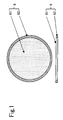
- the present invention is a wafer for LED mounting (hereafter simply referred to as the "wafer") 6, characterized by consisting of a metal infiltrated ceramic composite 61 and a protective layer 62 formed around it (see Figure 1 ).
- the metal infiltrated ceramic composite comprises at least one selected from silicon carbide, aluminum nitride, silicon nitride, diamond and graphite, is formed by impregnating a porous body or powder compact having a porosity of 10 to 50 volume% with a metal, and preferably has a plate thickness of 0.05 to 0.5 mm, a surface roughness (Ra) of 0.01 to 0.5 ⁇ m, a three-point bending strength of at least 50 MPa, a thermal conductivity of 150 to 500 W/mK at a temperature of 25 °C, a thermal expansion coefficient of 4 to 9 x 10 -6 /K from a temperature of 25 °C to 150 °C, and a volume resistivity of 10 -9 to 10 -5 ⁇ m.
- the protective layer consists of at least one metal selected from Ni, Co, Pd, Cu, Ag, Au, Pt, Ti, W and Mo, or at least one ceramic selected from alumina, mullite, aluminum nitride and silicon nitride having a porosity of at most 3%, the thickness of the protective layer is preferably at most 3 mm (not including 0), and the volume occupancy of the protective layer is preferably at most 20 volume% (not including 0).
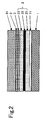
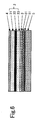
- the metal infiltrated ceramic composite 61 preferably has, on a surface, a thin layer 63 of a thickness of 0.5 to 10 ⁇ m and of at least one metal selected from Ni, Co, Pd, Cu, Ag, Au, Pt and Sn (see Figure 4 ).
- the thickness of the thin metal layer is preferably 0.5 to 10 ⁇ m; if it is less than 0.5 ⁇ m, the effect of enhancing chemical resistance may be poor, and if it exceeds 10 ⁇ m, surface roughness may be increased.
- the thin metal layer is formed by plating, such as non-electrolytic plating or electrolytic plating, or by vapor deposition etc.
- the present invention is a method for manufacturing the wafer of the present invention, comprising steps of loading into a metal or ceramic tubular body at least one selected from a porous ceramic body, a ceramic powder compact and a ceramic powder, then impregnating the pore of the at least one selected from a porous ceramic body, a ceramic powder compact and a ceramic powder with a metal, and then processing it.
- the present invention is a method for manufacturing the wafer of the present invention, comprising steps of impregnating the pore of a porous ceramic body or a ceramic powder compact with a metal, and then processing it after forming a protective layer on sides thereof, or forming a protective layer after processing.
- the present invention is an LED-mounted structure, characterized by sequentially having, on at least a surface of a substrate for LED mounting 5 consisting of at least a piece cut out from a part of the metal infiltrated ceramic composite 61 of the wafer of the present invention, a thin metal layer 51 (or a thin metal layer 51 and a metal layer 31 of a reflective layer), a reflective layer 3, an LED 2 and a transparent conductive layer 4, an electrode (not shown) being attached on the transparent conductive layer 4 (see Figure 3 and Figure 6 ).
- the wafer of the present invention one with a small difference in thermal expansion coefficient from LEDs is provided. At least a piece is cut out from a part of the metal infiltrated ceramic composite constituting the wafer of the present invention to form a substrate for LED mounting. Moreover, an LED is mounted on the substrate for LED mounting to form an LED-mounted structure. Additionally, the wafer of the present invention has excellent chemical resistance against acids and alkalis used during the manufacture of the LED-mounted structure of the present invention, and allows for easy formation of electrodes because of the high conductivity. Further, the LED-mounted structure of the present invention is one with high output and has excellent heat dissipation and reliability, and it is possible to increase the amount of luminescence per unit area. According to the method for manufacturing a wafer of the present invention, the wafer of the present invention can be easily manufactured.
- the LED-mounted structure of the present invention can be manufactured via, for example, the following steps: epitaxially growing an LED on a surface of a monocrystalline growth substrate (step a), joining it with the wafer of the present invention to produce a joined body (step b), removing the monocrystalline growth substrate part from the joined body to produce an intermediate structure (step c), and forming a transparent conductive layer and electrode etc. on the intermediate structure and then cutting it (step d).
- step a epitaxially growing an LED on a surface of a monocrystalline growth substrate
- step b joining it with the wafer of the present invention to produce a joined body
- step c removing the monocrystalline growth substrate part from the joined body to produce an intermediate structure
- step d forming a transparent conductive layer and electrode etc.
- Step a This step is a step of epitaxially growing an LED on a surface of a monocrystalline growth substrate. Specifically, after forming an n-type Group III-V semiconductor buffer layer 11 or a surface coating layer 12 of an inorganic compound on a surface of monocrystalline growth substrate 1, an LED 2 is epitaxially grown (see Figure 2 and Figure 5 ).
- the monocrystalline growth substrate For the monocrystalline growth substrate 1, one with a small difference in lattice constant from the LED and few defects is used.
- the monocrystalline growth substrate is preferably one of monocrystalline sapphire, monocrystalline silicon carbide, monocrystalline GaAs and monocrystalline Si.
- the thickness of the monocrystalline growth substrate is preferably 0.1 to 1.0 mm.
- monocrystalline growth substrate 1 preferably has, on a surface thereof, a buffer layer 11 composed of one of GaN, GaAs and GaP.
- the thickness of the buffer is preferably 0.1 to 0.8 ⁇ m.
- monocrystalline growth substrate 1 preferably has, on a surface thereof, a surface coating layer 12 composed of at least one inorganic compound selected from AIN, SiC, GaN and GaAs.
- the thickness of the surface coating layer is preferably 0.1 to 0.8 ⁇ m.
- LED 2 is usually constituted by an n-type Group III-V semiconductor layer 21, a luminescent layer 22, and a p-type Group III-V semiconductor layer 23, the present invention is not limited thereby.
- Such an LED can be formed by epitaxial growth by, for example, metal organic chemical vapor deposition (MOCVD) or halide vapor phase epitaxy (HVPE).
- MOCVD metal organic chemical vapor deposition
- HVPE halide vapor phase epitaxy
- the surface may be subjected to treatment such as etching or polishing.
- the thickness of the LED is preferably 0.6 to 15 ⁇ m.
- the thicknesses of n-type Group III-V semiconductor layer 21, luminescent layer 22, and p-type Group III-V semiconductor layer 23 are in general 0.3 to 10 ⁇ m, 0.1 to 0.5 ⁇ m and 0.3 to 10 ⁇ m respectively.
- Step b This step is a step of manufacturing a joined body of LED 2 epitaxially grown on the monocrystalline growth substrate as described above and wafer 6 of the present invention. Specifically, after forming a reflective layer 3 consisting of a metal on a surface of p-type Group III-V semiconductor layer 23 of the LED (see Figure 2 ), or after further forming a metal layer 31 on the surface of the reflective layer 3 as necessary (see Figure 5 ), it is joined with the wafer of the present invention.
- the wafer of the present invention shall be described below.
- Joining is performed by forming reflective layer 3 consisting of a metal (or reflective layer 3 and metal layer 31) on a surface of the metal infiltrated ceramic composite 61 of the wafer of the present invention, or on the surface of thin metal layer 63 formed on a surface thereof, then bringing the reflective layer 3 portion (or metal layer 31 portion) into contact with the above reflective layer 3 or the above metal layer 31, and heating them. By heating them, the two reflective layers 3 (or two metal layers 31) become integrated and form one reflective layer 3 (or one reflective layer 3 and one metal layer 31) (see Figure 6 ). Heating is preferably performed while applying pressure at 20 MPa or below. The heating temperature is selected from a range of 250 to 550 °C depending on the types of reflective layer 3, metal layer 31 of the reflective layer, and thin metal layer 63.
- metal layer 31 of the reflective layer is not necessarily required, but when they are constituted by dissimilar metals, the surface of reflective layer 3 preferably has a metal layer 31 of the reflective layer of the same type as thin metal layer 63. Vapor deposition or sputtering etc. is adopted to form reflective layer 3 and metal layer 31 of the reflective layer.
- the preferred metal species for these layers are indium, aluminum, gold, silver, and alloys thereof.
- reflective layer 3 and thin metal layer 63 are preferably constituted by the same type of metal species.
- the thickness of reflective layer 3 and metal layer 31 of the reflective layer since adhesion may be reduced if they are extremely thick, they are preferably 0.5 to 10 ⁇ m each, and particularly preferably 0.5 to 2 ⁇ m each. Even with these thicknesses, the thickness of reflective layer 3 is preferably the same as the thickness of thin metal layer 63 or within 10% thereof. The thickness of thin metal layer 63 is as described above.
- Step c This step is a step of removing monocrystalline growth substrate 1, buffer layer 11 and surface coating layer 12 from the above joined body.
- the removal of the monocrystalline growth substrate is performed by shining a laser, polishing or etching etc. from the side of the monocrystalline growth substrate.
- the buffer layer is removed by etching etc., and the surface coating layer is removed by a grinding process etc.
- the joined body is changed into an intermediate structure consisting of reference numbers 2, 3 (or 3 and 31) and 6 by this step.
- Step d This step is a step of surface finishing the exposed n-type Group III-V semiconductor layer 21 of the above intermediate structure, then forming a transparent conductive layer 4 and an electrode (not shown) on the transparent conductive layer, and then cutting into a desired shape to manufacture the LED-mounted structure of the present invention (see Figure 6 ). With the cutting, metal infiltrated ceramic composite 61 becomes substrate for LED mounting 5, and thin metal layer 63 becomes thin metal layer 51 on the surface of the substrate for LED mounting.
- n-type Group III-V semiconductor layer 21 is preferably performed by ICP dry etching to thereby flatten it to a surface suitable for the formation of a transparent conductive layer.
- the transparent conductive layer is formed to disperse electric current, and is formed by electron beam vapor deposition or sputtering etc. to have a thickness of 0.05 to 0.8 ⁇ m.
- the material of the transparent conductive layer is preferably at least one metal selected from indium tin oxide, cadmium tin oxide, indium zinc oxide, aluminum zinc oxide, tin zinc oxide and tin antimony oxide. Vapor deposition or sputtering is used to form the electrode.
- the material of the electrode is selected from Au, Ag and Al etc. Cutting is performed by laser cutting or dicing etc.
- the LED-mounted structure of the present invention can be manufactured by initially cutting out at least a piece (i.e. substrate for LED mounting) from a part of the metal infiltrated ceramic composite, and operating according to the above steps using the piece (though the cutting operation of step d will not be necessary). However, when considering productivity, manufacture by the above steps is preferred.
- Wafer 6 of the present invention is constituted by metal infiltrated ceramic composite 61 and protective layer 62 formed around it. LED is mounted on at least one piece cut out from a part of the above metal infiltrated ceramic composite, i.e. on substrate for LED mounting 5. From this point of view, the wafer of the present invention functions as a base material for the substrate for LED mounting.
- metal infiltrated ceramic composite 61 shall be explained.
- the necessary requirements of a substrate for LED mounting are: (a) having a strength that can endure the joining of a monocrystalline growth substrate on which the LED is epitaxially grown and the substrate for LED mounting, (b) the joining surface being flat without any pore or inclusion of foreign substances on the joining surface, (c) having good heat dissipation, and (d) having appropriate thermal conductivity and thermal expansion coefficient.
- (a) can be satisfied by making the three-point bending strength of the metal infiltrated ceramic composite at least 50 MPa
- (b) can be satisfied by making the surface roughness (Ra) 0.01 to 0.5 ⁇ m
- (c) can be satisfied by making the plate thickness of the metal infiltrated ceramic composite 0.05 to 0.5 mm
- (d) can be satisfied by using a metal infiltrated ceramic composite manufactured by impregnating a porous ceramic body or a ceramic powder compact comprising at least one selected from silicon carbide, aluminum nitride, silicon nitride, diamond and graphite and having a porosity of 10 to 50 volume% with a metal.
- the preferred types of metals for impregnation are aluminum alloys in which aluminum is the main component, the particularly preferred three-point bending strength is 200 to 400 MPa, the particularly preferred surface roughness (Ra) is 0.01 to 0.2 ⁇ m, the particularly preferred plate thickness is 0.08 to 0.3 mm, and the particularly preferred porosity of the above porous ceramic body is 15 to 35 volume%. Additionally, the preferred thermal conductivity of the metal infiltrated ceramic composite is 150 to 500 W/mK (at a temperature of 25 °C).
- the preferred thermal expansion coefficient is 4 to 9 x 10 -6 /K (from a temperature of 25 °C to 150 °C), and the particularly preferred thermal expansion coefficient is 4.5 to 8 x 10 -6 /K (from a temperature of 25 °C to 150 °C).
- the preferred volume resistivity of the metal infiltrated ceramic composite is less than 10 -5 ⁇ m.
- the three-point bending strength of the metal infiltrated ceramic composite is less than 50 MPa, it may not withstand the stress generated at each step of the manufacture of the LED-mounted structure.
- the surface roughness (Ra) is less than 0.01 ⁇ m, processing is difficult, which is associated with increased costs, and when it exceeds 0.5 ⁇ m, the adhesion with LED may decrease.
- the plate thickness is less than 0.05 mm, handling at each step of the manufacture of the LED-mounted structure is difficult, and when it exceeds 0.5 mm, the costs of processing into a final shape increase.
- the porosity of the above porous ceramic body is less than 10 volume% (the metal being less than 10 volume%), thermal conductivity is small, and when it exceeds 50 volume% (the metal exceeding 50 volume%), the thermal expansion coefficient of the metal infiltrated ceramic composite may be large.
- the thermal expansion coefficient of the metal infiltrated ceramic composite (from a temperature of 25 °C to 150 °C) is outside the range of 4 to 9 x 10 -6 /K, warping may occur after joining due to the difference in thermal expansion coefficient with the LED, and when used as an LED-mounted structure, peeling may occur to the joined layer, and further, the LED may crack. Additionally, when the thermal conductivity (at a temperature of 25 °C) is less than 150 W/mK, heat generated in the LED cannot be sufficiently dissipated, and in particular, for high-output LEDs where a large electrical current passes through, the temperature of the LED increases, luminescent efficiency decreases, and in connection therewith, the lifespan of the elements may decrease.
- the wafer While it may exceed 500 W/mK, the wafer will be expensive.
- the volume resistivity is 10 -5 ⁇ m or higher, luminescent efficiency may decrease.
- the lower limit of the volume resistivity is preferably 10 -9 ⁇ m.
- the three-point bending strength of the metal infiltrated ceramic composite can be increased or decreased by the granularity and content of silicon carbide, aluminum nitride, silicon nitride, diamond and graphite, and the surface roughness (Ra) and plate thickness can be increased or decreased by processing conditions.
- the thermal conductivity and thermal expansion coefficient can be increased or decreased by the porosity of the above porous ceramic body or of the above ceramic powder compact, and the type and content of the metal.
- the volume resistivity can be increased or decreased by the type and content of the metal for impregnation.
- the metal infiltrated ceramic composite itself has conductivity, an electrode can be easily formed on the LED. While for a monocrystalline growth substrate such as a sapphire substrate, the upper portion of the LED needs to be removed by etching etc. before forming an electrode on the same side, this operation is not needed when using a piece cut out from the metal infiltrated ceramic composite (substrate for LED mounting). As a result thereof, the amount of luminescence per unit area of the LED can be increased.
- the substrate for LED mounting i.e. a piece cut out from a part of the metal infiltrated ceramic composite of the wafer of the present invention
- the substrate for LED mounting i.e. a piece cut out from a part of the metal infiltrated ceramic composite of the wafer of the present invention
- chemical resistance refers to weight reduction per unit area that, when immersed for 1 minute in a 5N HCI solution at a temperature of 25 °C or in a 10N NaOH solution at a temperature of 75 °C, is at most 0.2 mg/cm 2 , particularly at most 0.1 mg/cm 2 for either chemical.
- the metal component of the substrate for LED mounting may elute during the process of manufacturing the LED-mounted structure, decreasing thermal conductivity etc., and problems such as chipping when cutting into a predetermined shape using laser cutting or dicing etc. and reduced yield of the LED-mounted structure may occur.
- the chemical resistance may be provided by forming a thin metal layer 51 on substrate for LED mounting 5. Additionally, since the sides of wafer 6 have a protective layer 62, when the protective layer is particularly at least one metal selected from Ni, Co, Pd, Cu, Ag, Au, Pt, Ti, W and Mo, or at least one ceramic having a porosity of at most 3% selected from aluminum nitride and silicon nitride, in particular alumina or mullite with a porosity of at most 3%, a particularly high chemical resistance is achieved.
- the thickness of protective layer 62 is preferably at most 3 mm (not including 0) and the volume occupancy of the protective layer is preferably at most 20 volume% (not including 0).
- the lower limit of the thickness and the lower limit of the volume occupancy of the protective layer are not particularly limited, and it only needs to have a thickness that can protect the metal infiltrated ceramic composite from external factors such as impacts during processing.
- the thickness exceeds 3 mm or when the volume occupancy exceeds 20 volume% the part of the metal infiltrated ceramic composite of the wafer decreases, so the yield of the LED-mounted structure of the present invention decreases, and further, peeling may occur due to the thermal expansion coefficients of the metal infiltrated ceramic composite and the protective layer.
- the particularly preferred thickness of the protective layer is 0.002 to 2 mm, and the particularly preferred volume occupancy is 0.1 to 15 volume%.
- the metal infiltrated ceramic composite may be manufactured by a method such as impregnation or powder metallurgy. A relatively higher thermal conductivity can be easily obtained by impregnation. Even for impregnation, there are methods performed under normal pressure and methods performed under a high pressure (high pressure forging), and high pressure forging includes liquid metal forging and die casting. For forming a protective layer around a metal infiltrated ceramic composite as in the present invention, liquid metal forging is particularly preferred. Moreover, liquid metal forging is a method in which a ceramic powder, a ceramic powder compact or a porous ceramic body is loaded in to a high pressure container, then the pore thereof are infiltrated with a molten metal such as an aluminum alloy under a high temperature and high pressure.
- the ceramic is preferably at least one selected from silicon carbide, aluminum nitride, silicon nitride, diamond and graphite.
- Thermal conductivity and thermal expansion coefficient can be adjusted by the type of ceramic, the type of metal and the component ratio thereof.
- the ceramic even in the form of a powder, can be composited with a metal, a ceramic powder compact made using a ceramic powder and, for example, a binder such as methyl cellulose or silica sol, or further, a porous ceramic body having a porosity of 10 to 50 volume% made by sintering the ceramic powder compact, is preferred.
- the shape is not particularly limited and may be a plate or cylinder etc.
- a general method for forming ceramic powder such as press molding or cast molding may be used.
- the porosity of the porous ceramic body may be adjusted by the granularity of the ceramic powder, molding pressure and sintering conditions etc.
- one or more of the loaded products are fixed with a jig coated with a mold release agent.
- a plurality of these loaded products may be stacked with mold release plates, such as stainless steel plates or ceramic plates coated with a mold release agent, in between, then connected using metal or ceramic bolts and nuts to form a stacked body.
- mold release plates such as stainless steel plates or ceramic plates coated with a mold release agent
- Graphite, boron nitride or alumina etc. may be used in the mold release agent.
- a molten metal heated to the melting point or above is added and a pressure of at least 30 MPa is applied to impregnate the pore of at least one selected from a ceramic powder, ceramic powder compact and porous ceramic body with the metal.
- a metal infiltrated ceramic composite is formed. Deformation during impregnation can be removed by subjecting the metal infiltrated ceramic composite to an annealing treatment.
- the heating temperature is less than 600 °C, or when the pressure during impregnation is less than 30 MPa, the thermal conductivity of the metal infiltrated ceramic composite may decrease. Additionally, when the temperature exceeds 800 °C, oxidation may occur on the surface of the ceramic, and this may contribute to the thermal conductivity.
- An impregnation pressure of 50 to 150 MPa is particularly preferred.
- the metal for impregnating the metal infiltrated ceramic composite is preferably an aluminum alloy magnesium alloy, copper alloy or a silicon alloy.
- An aluminum alloy comprising at least 70 mass% of aluminum is particularly preferred. When the aluminum content is less than 70 mass%, the thermal conductivity does not greatly improve. Additionally, for sufficient penetration of the pore, the aluminum alloy preferably has a melting point that is as low as possible.
- An example of such an aluminum alloy is an aluminum alloy comprising 5 to 25 mass% of silicon. Moreover, the inclusion of at most 5 mass% of magnesium makes the bond between the ceramic and metal stronger and is thus preferred.
- the resulting infiltrated product is processed using a lathe or cylindrical grinder etc., or if necessary, using a diamond whetstone, into a cylindrical shape where the tubular body surrounding the metal infiltrated ceramic composite is exposed. While the structure of the wafer is also adjusted by the dimensions of the inner diameter of the tubular body, the amount of grinding during this processing adjusts the dimensions of the outer diameter of the cylindrical body to adjust the final shape of the wafer. In other words, the thickness of the protective layer is determined by volume occupancy.
- a separate method in which the pore of a porous ceramic body or ceramic powder compact are first infiltrated with a metal, and then a protective layer is formed on its sides may be used.
- a molten metal heated to above the melting point is added and a pressure of at least 30 MPa is applied to impregnate the pore of the ceramic powder compact or porous ceramic body with the metal.
- the resulting infiltrated product is processed using a lathe or cylindrical grinder etc., or if necessary, by using a diamond whetstone, into a cylindrical body. Then at least one protective layer selected from Ni, Co, Pd, Cu, Ag, Au, Pt, Ti, W and Mo is formed around it (on the sides) by plating, vapor deposition or sputtering.
- the surface is finished to form the wafer of the present invention.
- That the wafer of the present invention may have a thin layer 63 of at least one metal selected from Ni, Co, Pd, Cu, Ag, Au, Pt and Sn was described above. While the cutting method is not particularly limited, multi-wire saws which have low cutting costs and are suitable for mass production are preferred.
- a processing machine such as a double-sided grinder, rotary grinder, surface grinder or lapping machine be used to surface finish it to a plate thickness of 0.05 to 0.5 mm and a surface roughness (Ra) of 0.01 to 0.5 ⁇ m.
- a processing machine such as a double-sided grinder, rotary grinder, surface grinder or lapping machine be used to surface finish it to a plate thickness of 0.05 to 0.5 mm and a surface roughness (Ra) of 0.01 to 0.5 ⁇ m.
- SiC silicon carbide
- this porous ceramic body After inserting this porous ceramic body into an alumina tube (outer diameter dimensions: ⁇ 52.3 mm x 100 mm, inner diameter dimensions: ⁇ 49 mm x 100 mm), it was inserted into a tubular graphite jig coated with a boron nitride mold release agent (external dimensions: 70 mm x 70 mm x 100 mm, inner diameter dimensions: ⁇ 52.5 mm x 100 mm) to form a structure.
- a boron nitride mold release agent external dimensions: 70 mm x 70 mm x 100 mm, inner diameter dimensions: ⁇ 52.5 mm x 100 mm
- mold release plates stainless steel plates of 70 mm x 100 mm x 0.8 mm coated with a graphite mold release agent
- 12 mm-thick iron plates were placed on two sides, and they were connected with eight bolts to form one stacked body (140.8 mm x 140.8 mm x 100 mm).
- the stacked body After preheating the stacked body to a temperature of 700 °C in an electric furnace, it was stored in a pre-heated press mold (inner diameter ⁇ 400 mm x 300 mm), a molten aluminum alloy (alloy composition: Si 12 mass%, Mg 1 mass%, Al 87 mass%, and temperature: 800 °C) was poured into it, and a pressure of 100 MPa was applied for 25 minutes to impregnate it with the aluminum alloy.
- a molten aluminum alloy alloy (alloy composition: Si 12 mass%, Mg 1 mass%, Al 87 mass%, and temperature: 800 °C) was poured into it, and a pressure of 100 MPa was applied for 25 minutes to impregnate it with the aluminum alloy.
- the mold release plates were stripped using a wet bandsaw along the shape of the mold release plates, and after removing the graphite jig portion by a lathe, a 3-hour annealing treatment was performed at a temperature of 530 °C, deformation was removed, and an infiltrated product (a cylindrical body of ⁇ 52 mm x 100 mm) was manufactured.
- a test piece for measuring thermal expansion coefficient ( ⁇ 3 mm x 10 mm), a test piece for measuring thermal conductivity (25 mm x 25 mm x 1 mm), a test piece for measuring three-point bending strength (3 mm x 4 mm x 40 m), and a test piece for measuring volume resistivity (40 mm x 40 mm x 5 mm) were cut out by a grinding process, and thermal expansion coefficient from a temperature of 25 °C to 150 °C was measured by a thermal expansion meter (manufactured by Seiko Instruments Inc.; TMA 300), thermal conductivity at a temperature of 25 °C was measured by laser flashing (manufactured by Ulvac; TC3000), three-point bending strength was measured by a bending strength tester, and volume resistivity was measured by the four-point probe method (in accordance with JIS R1637).
- the results were that the thermal expansion coefficient was 5.1 x 10 -6 /K, the thermal conductivity was
- This wafer 6 consists of a center portion of a metal infiltrated ceramic composite 61 and an alumina protective layer 62 around it (see Figure 1 ).
- the surface roughness (Ra) measured by a surface roughness meter was 0.08 ⁇ m
- the thickness of the alumina protective layer measured by an industrial microscope was 0.9 mm
- the volume occupancy of the protective layer was 7.0%.
- a thin metal layer 63 (0.5 ⁇ m-thick Au layer) was formed by vapor deposition on the top and bottom surfaces of the wafer (see Figure 4 ), and chemical resistance was evaluated. Chemical resistance was measured by immersing for 1 minute in a 5N HCI solution at a temperature 25 °C, then washing with distilled water, further immersing for 1 minute in a 10N NaOH solution at a temperature of 75 °C, then washing with water, measuring the mass, and calculating weight reduction per unit area. The result was 0.01 mg/cm 2 .
- n-type GaN buffer layer 11 As shown in Figure 2 , a 0.3 ⁇ m n-type Group III-V semiconductor buffer layer (n-type GaN buffer layer) 11 was formed on a monocrystalline growth substrate (monocrystalline sapphire substrate) 1 with a plate thickness of 0.5 mm by MOCVD at a temperature of 1100 °C using ammonia gas and trimethyl gallium and using a mixed gas of nitrogen and hydrogen as carrier gas, then a 4.1 ⁇ m LED 2 was epitaxially grown thereon.
- the LED was composed of 2 ⁇ m of an n-type Group III-V semiconductor layer (n-type GaN semiconductor layer) 21, 0.1 ⁇ m of a luminescent layer (GaN luminescent layer) 22, and 2 ⁇ m of a p-type Group III-V semiconductor layer (p-type GaN semiconductor layer) 23.
- a 2 ⁇ m-thick reflective layer 3 of a metal layer of a silver/tin alloy (Ag 3.5 mass%, Sn 96.5 mass%) was respectively vacuum vapor deposited on the surface of the p-type GaN semiconductor layer 23 of LED 2 and a surface of wafer 6 of the present invention manufactured above.
- the above reflective layers 3 were stacked in contact with each other and kept for 5 minutes under a pressure of 5 MPa at a temperature of 400 °C.
- the two reflective layers fused together to form one reflective layer 3.
- Monocrystalline sapphire substrate 1 was stripped from the resulting joined body from the side of the monocrystalline growth substrate (monocrystalline sapphire substrate) by shining a nitrogen gas laser with an output of 40 MW/cm 2 . Additionally, by shining the laser, n-type GaN buffer layer 11 disintegrated into Ga and nitrogen, and the monocrystalline sapphire substrate was stripped by the nitrogen gas generated thereby.
- the joined body changed into an intermediate structure consisting of reference numbers 2, 3 and 6 by this step.
- Thin layers 63 of various metals were formed on wafers manufactured in Example 1 (see Figure 4 ), and chemical resistance was evaluated. Results thereof are shown in Table 2.
- Porous ceramic bodies (porosity: 20%) manufactured in Example 1 were processed to have outer diameter dimensions shown in Table 3 by a machining center using a diamond whetstone. After each of these were inserted into a metal or ceramic tubular body (outer diameter dimensions: ⁇ 52.3 mm x 100 mm, inner diameter dimensions: Table 3), they were placed in tubular graphite jigs (external dimensions: 70 mm x 70 mm x 100 mm, inner diameter dimensions: ⁇ 52.5 mm x 100 mm) using a boron nitride mold release agent to form structures, and then subjected to operations until the annealing treatment in a manner similar to those in Example 1 to manufacture metal infiltrated ceramic composites.
- wafers having a shape of ⁇ 50.8 mm x 0.2 mm and a surrounding protective layer of a material corresponding to a metal or ceramic tubular body were manufactured in a manner similar to that in Example 1 from the metal infiltrated ceramic composites. Results thereof are shown in Table 3.
- a wafer was manufactured in a manner similar to that in Example 1 from the metal infiltrated ceramic composite; however, the surface roughness (Ra) of the wafer was Ra 0.06 ⁇ m, the thickness of the alumina protective layer was 0.9 mm, the volume occupancy was 7.0% and the chemical resistance was 0.01 mg/cm 2 .
- a mixed powder of 2000 g of a silicon carbide powder D (commercial product: average particle diameter 10 ⁇ m) and 300 g of silica sol (manufactured by Nissan Chemical Industries, Ltd.: Snowtex) was press molded into a cylindrical shape with dimensions of ⁇ 52 x 100 mm at a surface pressure of 30 MPa to manufacture a molded body.
- silica sol manufactured by Nissan Chemical Industries, Ltd.: Snowtex
- the thermal expansion coefficient of the metal infiltrated ceramic composite was 9.5 x 10 -6 /K
- the thermal conductivity was 180 W/mK
- the three-point bending strength was 500 MPa
- the volume resistivity was 3 x 10 -7 ⁇ m.
- a wafer was manufactured in a manner similar to that in Example 1 from the metal infiltrated ceramic composite; however, the surface roughness (Ra) was Ra 0.09 ⁇ m, the thickness of the alumina protective layer was 0.9 mm, the volume occupancy was 7.0% and the chemical resistance was 0.02 mg/cm 2 .
- a mixed powder of 138 g of a silicon carbide powder D and 255 g of a silicon carbide powder E (commercial product: average particle diameter 150 ⁇ m) into an alumina tube (outer diameter dimensions: ⁇ 52.3 mm x 100 mm, inner diameter dimensions: ⁇ 49 mm x 100 mm) to form a ceramic powder compact (porosity: 35%), and then inserting it into a tubular graphite jig to form a structure, operations until the annealing treatment were performed in a manner similar to those in Example 1 to manufacture a metal infiltrated ceramic composite.
- the thermal expansion coefficient of the metal infiltrated ceramic composite was 7.5 x 10 -6 /K
- the thermal conductivity was 210 W/mK
- the three-point bending strength was 400 MPa
- the volume resistivity was 5 x 10 -7 ⁇ m.
- a wafer was manufactured from the metal infiltrated ceramic composite in a manner similar to that in Example 1; however, the surface roughness (Ra) was 0.08 ⁇ m, the thickness of the alumina protective layer was 0.9 mm, the volume occupancy was 7.0% and the chemical resistance was 0.01 mg/cm 2 .
- a porous ceramic body manufactured in Example 1 was processed to a shape with external dimensions of ⁇ 52 mm x 100 mm by a machining center using a diamond whetstone, then it was coated with a boron nitride mold release agent and inserted into a tubular iron jig (external dimensions: 70 mm x 70 mm x 100 mm, inner diameter dimensions: ⁇ 52.5 mm x 100 mm) to form a structure.
- the resulting metal infiltrated ceramic composite After outer periphery processing the resulting metal infiltrated ceramic composite into a cylindrical shape of ⁇ 50.8 mm x 100 mm by a cylindrical grinder using a diamond whetstone, the surface was cleaned, then the aluminum alloy portion on the surface was removed by etching using a NaOH solution, and non-electrolytic plating was performed to form a 10 ⁇ m-thick Ni-P plated layer. Then the cylindrical metal infiltrated ceramic composite was cut into a disk with a plate thickness of 0.3 mm by a multi-wire saw using diamond grains at a slicing speed of 0.2 mm/min.
- the disk-shaped metal infiltrated ceramic composite After grinding the disk-shaped metal infiltrated ceramic composite into a plate thickness of 0.22 mm by a double-sided grinder using a #600 diamond whetstone, it was polished to a plate thickness of 0.2 mm by a lapping machine using diamond grains, then it was subjected to supersonic cleansing in pure water and then in isopropyl alcohol and dried to manufacture a wafer 6 consisting of a center portion of a metal infiltrated ceramic composite 61 and a protective layer 62 of a metal layer (Ni) around it (see Figure 1 ).
- the surface roughness (Ra) of the wafer was Ra 0.09 ⁇ m
- the thickness of the Ni protective layer was 0.01 mm
- the volume occupancy was 0.04%
- the chemical resistance was 0.01 mg/cm 2 .
- LED 2 was epitaxially grown by HVPE at a temperature of 1050 °C using ammonia gas and gallium chloride and using hydrogen gas as a carrier gas.
- LED 2 was composed of 2 ⁇ m of an n-type Group III-V semiconductor layer (n-type GaN semiconductor layer) 21, 0.1 ⁇ m of a luminescent layer (GaN luminescent layer) 22 and 2 ⁇ m of a p-type Group III-V semiconductor layer (p-type GaN semiconductor layer) 23.
- an Au/tin alloy (Au 80 mass%, Sn 20 mass%) was vapour deposited to a thickness of 1.5 ⁇ m to form a metal layer 31.
- a metal layer 31 was formed on a surface of wafer 6 manufactured above by vapour depositing an Au/tin alloy to a thickness of 1.5 ⁇ m.
- the two metal layers 31 were stacked facing each other and kept for 5 minutes under a pressure of 5 MPa at a temperature of 500 °C to manufacture a joined body. The two metal layers 31 fused to form one metal layer 31 by this step.
- the metal infiltrated ceramic composite After cutting the metal infiltrated ceramic composite with a diamond saw, it was outer periphery processed to a cylindrical shape of diameter 50.8 mm x 100 mm by a cylindrical grinder using a diamond whetstone, and a wafer having a protective layer of a metal layer (Ni) around it was manufactured in a manner similar to that in Example 26.
- the surface roughness (Ra) of the wafer was 0.15 ⁇ m
- the thickness of the Ni protective layer was 0.01 mm
- the volume occupancy was 0.04
- the chemical resistance was 0.02 mg/cm 2 .
- the thermal expansion coefficient of the metal infiltrated ceramic composite was 5.3 x 10 -6 /K, the thermal conductivity was 180 W/mK, the three-point bending strength was 420 MPa, and the volume resistivity was 7.5 x 10 -7 ⁇ m. Then a wafer was manufactured in a manner similar to that in Example 27 from the metal infiltrated ceramic composite.
- the surface roughness (Ra) of the wafer was 0.07 ⁇ m
- the thickness of the Ni protective layer was 0.01 mm
- the volume occupancy was 0.04%
- the chemical resistance was 0.01 mg/cm 2 .
- a CIP molded body was manufactured in a manner similar to that in Example 28. After firing it for 4 hours at a temperature of 1880 °C under a 0.9 MPa pressurized nitrogen atmosphere to manufacture a sintered body, a porous ceramic body (diameter 52 mm x 100 mm) with a porosity of 13% was manufactured by a machining center using a diamond whetstone.
- a metal infiltrated ceramic composite and a wafer were manufactured in a manner similar to those in Example 28.
- the thermal expansion coefficient of the metal infiltrated ceramic composite was 4.0 x 10 -6 /K
- the thermal conductivity was 150 W/mK
- the three-point bending strength was 450 MPa
- the volume resistivity was 1.1 x 10 -6 ⁇ m.
- the surface roughness (Ra) of the wafer was Ra 0.09 ⁇ m
- the thickness of the Ni protective layer was 0.01 mm
- the volume occupancy was 0.04%
- the chemical resistance was 0.01 mg/cm 2 .
- the ceramic powder compact was made into a stacked body, which was subjected to an impregnation treatment in accordance with Example 1 to manufacture a metal infiltrated ceramic composite (70 mm x 70 mm x 20 mm) surrounded by a tubular graphite jig.
- the thermal expansion coefficient of the metal infiltrated ceramic composite was 7.5 x 10 -6 /K
- the thermal conductivity was 500 W/mK
- the three-point bending strength was 320 MPa
- the volume resistivity was 5 x 10 -7 ⁇ m.
- a grinding process was performed by a surface grinder using a diamond whetstone from the two main sides (70 mm x 70 mm) to process it into a plate-shaped body (70 mm x 70 mm x 3 mm).
- a porous ceramic body (external dimensions: diameter 52 mm x height 100 mm, porosity: 20%) of Example 1 was processed into a disk with external dimensions of diameter 52 mm x 20 mm by a machining center using a diamond whetstone.
- the disk and a lump of silicon were placed in a graphite crucible coated with a BN powder, and set inside an electric furnace. The inside was vacuumed and kept for 8 hours at 1650 °C to impregnate it with silicon. After cooling to room temperature, excess silicon was removed by a cylindrical grinder to manufacture a metal infiltrated ceramic composite.
- the thermal expansion coefficient of the metal infiltrated ceramic composite was 4.3 x 10 -6 /K, the thermal conductivity was 210 W/mK, the three-point bending strength was 250 MPa, and the volume resistivity was 1 x 10 -5 ⁇ m. Then a wafer was manufacture in a manner similar to that in Example 26.
- the surface roughness (Ra) of the wafer was 0.15 ⁇ m, the thickness of the Ni protective layer was 0.01 mm, the volume occupancy was 0.04% and the chemical resistance was 0.005 mg/cm 2 .
- Example 1 Plate Thickness (mm) Surface Roughness (Ra) ( ⁇ m) Thickness of Protective Layer (mm) Volume Occupancy of Protective Layer (volume%) Decrease in Mass (mg/cm 2 )
- Example 1 0.2 0.08 0.9 7.0 0.01
- Example 2 0.05 0.08 0.9 7.0 0.02
- Example 3 0.5 0.08 0.9 7.0 0.01
- Example 4 0.2 0.01 0.9 7.0 0.01
- Example 5 0.2 0.5 0.9 7.0 0.03 Comparative Example 1 0.02 0.09 0.9 7.0 0.2 Comparative Example 2 1 0.1 0.9 7.0 0.01 Comparative Example 3 0.2 1 0.9 7.0 0.1
Landscapes
- Chemical & Material Sciences (AREA)
- Engineering & Computer Science (AREA)
- Materials Engineering (AREA)
- Ceramic Engineering (AREA)
- Organic Chemistry (AREA)
- Structural Engineering (AREA)
- Mechanical Engineering (AREA)
- Metallurgy (AREA)
- Manufacturing & Machinery (AREA)
- Inorganic Chemistry (AREA)
- Led Devices (AREA)
- Led Device Packages (AREA)
- Container, Conveyance, Adherence, Positioning, Of Wafer (AREA)
- Chemical Kinetics & Catalysis (AREA)
- Electrochemistry (AREA)
- Physics & Mathematics (AREA)
- Cooling Or The Like Of Semiconductors Or Solid State Devices (AREA)
- General Chemical & Material Sciences (AREA)
- Plasma & Fusion (AREA)
- Fluid Mechanics (AREA)
Abstract
Description
- The present invention relates to a wafer for LED mounting, a method for manufacturing the wafer and an LED-mounted structure using the wafer.
- A light-emitting diode (LED) is an element that emits light when a forward current passes through the pn junction of a semiconductor, and is manufactured using a Group III-V semiconductor crystal such as GaAs or GaN. In recent years, through advances in epitaxial growth technology for semiconductors and light-emitting element processing technology, LEDs with excellent conversion efficiency have been developed and widely used in various fields.
- An LED is composed of a p-type layer and an n-type layer formed by epitaxially growing a Group III-V semiconductor crystal on a monocrystalline growth substrate, and a photoactive layer sandwiched between the two. In general, they are formed by epitaxially growing a Group III-V semiconductor crystal on a growth substrate such as a monocrystalline sapphire, then attaching electrodes thereto (Patent Document 1).
- In cases where a Group III-V semiconductor crystal is epitaxially grown on a monocrystalline growth substrate, since the monocrystalline growth substrate and Group III-V semiconductor crystal have different lattice constants, it is difficult to grow a good LED. For this reason, a method of forming a buffer layer such as GaN on a monocrystalline growth substrate at a low temperature, and then epitaxially growing GaN thereon has been proposed (Patent Document 2).
- On the other hand, there is the problem of poor thermal conductivity of monocrystalline growth substrates. In the case of monocrystalline sapphire, the thermal conductivity is approximately 40 W/mK, and the heat generated by a Group III-V semiconductor element cannot be sufficiently dissipated. In particular, for high-output LEDs where a large electrical current passes through, there are problems of increased temperature of the elements, reduced luminescent efficiency and reduced lifespan of the elements. For this reason, a method of epitaxially growing a Group III-V semiconductor crystal on a monocrystalline growth substrate, then joining it with a highly thermal conductive substrate via a metal layer, and then removing the monocrystalline growth substrate has been proposed (Patent Document 3). In this case, as the highly thermal conductive substrate, materials such as copper that have excellent thermal conductivity have been examined, but the difference in thermal expansion coefficient with Group III-V semiconductor crystals is large, and their use in high-output LEDs has not been sufficiently satisfactory.
- Patent Document 1:
JP-A 2005-117006 - Patent Document 2:
JP-B H5-73252 - Patent Document 3 :
JP-A 2006-128710 - The object of the present invention is to provide a wafer for LED mounting which has a small difference in thermal expansion coefficient from LEDs and excellent thermal conductivity, a method for manufacturing the wafer for LED mounting, and an LED-mounted structure manufactured using the wafer for LED mounting.
- The present invention is a wafer for LED mounting (hereafter simply referred to as the "wafer") 6, characterized by consisting of a metal infiltrated
ceramic composite 61 and aprotective layer 62 formed around it (seeFigure 1 ). - In the wafer of the present invention, the metal infiltrated ceramic composite comprises at least one selected from silicon carbide, aluminum nitride, silicon nitride, diamond and graphite, is formed by impregnating a porous body or powder compact having a porosity of 10 to 50 volume% with a metal, and preferably has a plate thickness of 0.05 to 0.5 mm, a surface roughness (Ra) of 0.01 to 0.5 µm, a three-point bending strength of at least 50 MPa, a thermal conductivity of 150 to 500 W/mK at a temperature of 25 °C, a thermal expansion coefficient of 4 to 9 x 10⁻⁶/K from a temperature of 25 °C to 150 °C, and a volume resistivity of 10-9 to 10-5 Ω·m.
- Additionally in the wafer of the present invention, the protective layer consists of at least one metal selected from Ni, Co, Pd, Cu, Ag, Au, Pt, Ti, W and Mo, or at least one ceramic selected from alumina, mullite, aluminum nitride and silicon nitride having a porosity of at most 3%, the thickness of the protective layer is preferably at most 3 mm (not including 0), and the volume occupancy of the protective layer is preferably at most 20 volume% (not including 0).
- Further, in the wafer of the present invention, the metal infiltrated
ceramic composite 61 preferably has, on a surface, athin layer 63 of a thickness of 0.5 to 10 µm and of at least one metal selected from Ni, Co, Pd, Cu, Ag, Au, Pt and Sn (seeFigure 4 ). The thickness of the thin metal layer is preferably 0.5 to 10 µm; if it is less than 0.5 µm, the effect of enhancing chemical resistance may be poor, and if it exceeds 10 µm, surface roughness may be increased. The thin metal layer is formed by plating, such as non-electrolytic plating or electrolytic plating, or by vapor deposition etc. - Additionally, the present invention is a method for manufacturing the wafer of the present invention, comprising steps of loading into a metal or ceramic tubular body at least one selected from a porous ceramic body, a ceramic powder compact and a ceramic powder, then impregnating the pore of the at least one selected from a porous ceramic body, a ceramic powder compact and a ceramic powder with a metal, and then processing it.
- Moreover, the present invention is a method for manufacturing the wafer of the present invention, comprising steps of impregnating the pore of a porous ceramic body or a ceramic powder compact with a metal, and then processing it after forming a protective layer on sides thereof, or forming a protective layer after processing.
- In addition, the present invention is an LED-mounted structure, characterized by sequentially having, on at least a surface of a substrate for
LED mounting 5 consisting of at least a piece cut out from a part of the metal infiltratedceramic composite 61 of the wafer of the present invention, a thin metal layer 51 (or a thin metal layer 51 and ametal layer 31 of a reflective layer), areflective layer 3, anLED 2 and a transparentconductive layer 4, an electrode (not shown) being attached on the transparent conductive layer 4 (seeFigure 3 andFigure 6 ). - According to the wafer of the present invention, one with a small difference in thermal expansion coefficient from LEDs is provided. At least a piece is cut out from a part of the metal infiltrated ceramic composite constituting the wafer of the present invention to form a substrate for LED mounting. Moreover, an LED is mounted on the substrate for LED mounting to form an LED-mounted structure. Additionally, the wafer of the present invention has excellent chemical resistance against acids and alkalis used during the manufacture of the LED-mounted structure of the present invention, and allows for easy formation of electrodes because of the high conductivity. Further, the LED-mounted structure of the present invention is one with high output and has excellent heat dissipation and reliability, and it is possible to increase the amount of luminescence per unit area. According to the method for manufacturing a wafer of the present invention, the wafer of the present invention can be easily manufactured.
-
- [
Figure 1 ] is a diagram of a wafer of the present invention manufactured in Example 1. - [
Figure 2 ] is a diagram of a joined body comprising the wafer ofFigure 1 and an LED. - [
Figure 3 ] is a diagram of an LED-mounted structure of the present invention manufactured from the joined body ofFigure 2 . - [
Figure 4 ] is a diagram of a wafer of the present invention manufactured in Example 26. - [
Figure 5 ] is a diagram of a joined body comprising the wafer ofFigure 4 and an LED. - [
Figure 6 ] is a diagram of an LED-mounted structure of the present invention manufactured from the joined body ofFigure 5 . -
- 1
- Monocrystalline growth substrate
- 11
- N-type Group III-V semiconductor buffer layer on a surface of
monocrystalline growth substrate 1 - 12
- Surface coating layer of an inorganic compound on a surface of
monocrystalline growth substrate 1 - 2
- LED
- 21
- N-type Group III-V semiconductor layer of
LED 2 - 22
- Luminescent layer of
LED 2 - 23
- P-type Group III-V semiconductor layer of
LED 2 - 3
- Reflective layer
- 31
- Metal layer on a surface of
reflective layer 3 - 4
- Transparent conductive layer
- 5
- Substrate for LED mounting
- 51
- Metal foil layer on a surface of substrate for LED mounting 5
- 6
- Wafer
- 61
- Metal infiltrated ceramic composite of
wafer 6 - 62
- Protective layer of
wafer 6 - 63
- Thin metal layer on a surface of metal infiltrated
ceramic composite 61 - The LED-mounted structure of the present invention can be manufactured via, for example, the following steps: epitaxially growing an LED on a surface of a monocrystalline growth substrate (step a), joining it with the wafer of the present invention to produce a joined body (step b), removing the monocrystalline growth substrate part from the joined body to produce an intermediate structure (step c), and forming a transparent conductive layer and electrode etc. on the intermediate structure and then cutting it (step d). Herebelow, it shall be explained with reference to the drawings.
- (Step a) This step is a step of epitaxially growing an LED on a surface of a monocrystalline growth substrate. Specifically, after forming an n-type Group III-V
semiconductor buffer layer 11 or asurface coating layer 12 of an inorganic compound on a surface ofmonocrystalline growth substrate 1, anLED 2 is epitaxially grown (seeFigure 2 andFigure 5 ). - For the
monocrystalline growth substrate 1, one with a small difference in lattice constant from the LED and few defects is used. To ensure the crystal properties and homogeneity of the LED, and to increase the durability against the atmosphere during epitaxial growth, the monocrystalline growth substrate is preferably one of monocrystalline sapphire, monocrystalline silicon carbide, monocrystalline GaAs and monocrystalline Si. The thickness of the monocrystalline growth substrate is preferably 0.1 to 1.0 mm. Additionally, to reduce the difference in lattice constant with the LED,monocrystalline growth substrate 1 preferably has, on a surface thereof, abuffer layer 11 composed of one of GaN, GaAs and GaP. The thickness of the buffer is preferably 0.1 to 0.8 µm. Additionally, in order to make the lattice constant of the monocrystalline growth substrate as close to that of the LED as possible,monocrystalline growth substrate 1 preferably has, on a surface thereof, asurface coating layer 12 composed of at least one inorganic compound selected from AIN, SiC, GaN and GaAs. The thickness of the surface coating layer is preferably 0.1 to 0.8 µm. - While
LED 2 is usually constituted by an n-type Group III-V semiconductor layer 21, aluminescent layer 22, and a p-type Group III-V semiconductor layer 23, the present invention is not limited thereby. Such an LED can be formed by epitaxial growth by, for example, metal organic chemical vapor deposition (MOCVD) or halide vapor phase epitaxy (HVPE). According to MOCVD, an LED with good crystal properties can be grown, and according to HVPE, since the speed of crystal growth is fast, an LED can be grown efficiently. In order to further improve the luminescence property of an epitaxially grown LED, the surface may be subjected to treatment such as etching or polishing. The thickness of the LED is preferably 0.6 to 15 µm. The thicknesses of n-type Group III-V semiconductor layer 21,luminescent layer 22, and p-type Group III-V semiconductor layer 23 are in general 0.3 to 10 µm, 0.1 to 0.5 µm and 0.3 to 10 µm respectively. - (Step b) This step is a step of manufacturing a joined body of
LED 2 epitaxially grown on the monocrystalline growth substrate as described above andwafer 6 of the present invention. Specifically, after forming areflective layer 3 consisting of a metal on a surface of p-type Group III-V semiconductor layer 23 of the LED (seeFigure 2 ), or after further forming ametal layer 31 on the surface of thereflective layer 3 as necessary (seeFigure 5 ), it is joined with the wafer of the present invention. The wafer of the present invention shall be described below. Joining is performed by formingreflective layer 3 consisting of a metal (orreflective layer 3 and metal layer 31) on a surface of the metal infiltratedceramic composite 61 of the wafer of the present invention, or on the surface ofthin metal layer 63 formed on a surface thereof, then bringing thereflective layer 3 portion (ormetal layer 31 portion) into contact with the abovereflective layer 3 or theabove metal layer 31, and heating them. By heating them, the two reflective layers 3 (or two metal layers 31) become integrated and form one reflective layer 3 (or onereflective layer 3 and one metal layer 31) (seeFigure 6 ). Heating is preferably performed while applying pressure at 20 MPa or below. The heating temperature is selected from a range of 250 to 550 °C depending on the types ofreflective layer 3,metal layer 31 of the reflective layer, andthin metal layer 63. - When
reflective layer 3 andthin metal layer 63 are constituted by the same type of metal,metal layer 31 of the reflective layer is not necessarily required, but when they are constituted by dissimilar metals, the surface ofreflective layer 3 preferably has ametal layer 31 of the reflective layer of the same type asthin metal layer 63. Vapor deposition or sputtering etc. is adopted to formreflective layer 3 andmetal layer 31 of the reflective layer. The preferred metal species for these layers are indium, aluminum, gold, silver, and alloys thereof. In particular,reflective layer 3 andthin metal layer 63 are preferably constituted by the same type of metal species. With respect to the thicknesses ofreflective layer 3 andmetal layer 31 of the reflective layer, since adhesion may be reduced if they are extremely thick, they are preferably 0.5 to 10 µm each, and particularly preferably 0.5 to 2 µm each. Even with these thicknesses, the thickness ofreflective layer 3 is preferably the same as the thickness ofthin metal layer 63 or within 10% thereof. The thickness ofthin metal layer 63 is as described above. - (Step c) This step is a step of removing
monocrystalline growth substrate 1,buffer layer 11 andsurface coating layer 12 from the above joined body. The removal of the monocrystalline growth substrate is performed by shining a laser, polishing or etching etc. from the side of the monocrystalline growth substrate. The buffer layer is removed by etching etc., and the surface coating layer is removed by a grinding process etc. The joined body is changed into an intermediate structure consisting ofreference numbers 2, 3 (or 3 and 31) and 6 by this step. - (Step d) This step is a step of surface finishing the exposed n-type Group III-
V semiconductor layer 21 of the above intermediate structure, then forming a transparentconductive layer 4 and an electrode (not shown) on the transparent conductive layer, and then cutting into a desired shape to manufacture the LED-mounted structure of the present invention (seeFigure 6 ). With the cutting, metal infiltrated ceramic composite 61 becomes substrate for LED mounting 5, andthin metal layer 63 becomes thin metal layer 51 on the surface of the substrate for LED mounting. - Surface finishing of n-type Group III-
V semiconductor layer 21 is preferably performed by ICP dry etching to thereby flatten it to a surface suitable for the formation of a transparent conductive layer. The transparent conductive layer is formed to disperse electric current, and is formed by electron beam vapor deposition or sputtering etc. to have a thickness of 0.05 to 0.8 µm. The material of the transparent conductive layer is preferably at least one metal selected from indium tin oxide, cadmium tin oxide, indium zinc oxide, aluminum zinc oxide, tin zinc oxide and tin antimony oxide. Vapor deposition or sputtering is used to form the electrode. The material of the electrode is selected from Au, Ag and Al etc. Cutting is performed by laser cutting or dicing etc. - In the present invention, the LED-mounted structure of the present invention can be manufactured by initially cutting out at least a piece (i.e. substrate for LED mounting) from a part of the metal infiltrated ceramic composite, and operating according to the above steps using the piece (though the cutting operation of step d will not be necessary). However, when considering productivity, manufacture by the above steps is preferred.
- Next, the wafer of the present invention and the manufacture method thereof shall be explained.
-
Wafer 6 of the present invention is constituted by metal infiltrated ceramic composite 61 andprotective layer 62 formed around it. LED is mounted on at least one piece cut out from a part of the above metal infiltrated ceramic composite, i.e. on substrate for LED mounting 5. From this point of view, the wafer of the present invention functions as a base material for the substrate for LED mounting. - First, metal infiltrated ceramic composite 61 shall be explained. The necessary requirements of a substrate for LED mounting are: (a) having a strength that can endure the joining of a monocrystalline growth substrate on which the LED is epitaxially grown and the substrate for LED mounting, (b) the joining surface being flat without any pore or inclusion of foreign substances on the joining surface, (c) having good heat dissipation, and (d) having appropriate thermal conductivity and thermal expansion coefficient. (a) can be satisfied by making the three-point bending strength of the metal infiltrated ceramic composite at least 50 MPa, (b) can be satisfied by making the surface roughness (Ra) 0.01 to 0.5 µm, (c) can be satisfied by making the plate thickness of the metal infiltrated ceramic composite 0.05 to 0.5 mm, and (d) can be satisfied by using a metal infiltrated ceramic composite manufactured by impregnating a porous ceramic body or a ceramic powder compact comprising at least one selected from silicon carbide, aluminum nitride, silicon nitride, diamond and graphite and having a porosity of 10 to 50 volume% with a metal.
- For the metal infiltrated ceramic composite, the preferred types of metals for impregnation are aluminum alloys in which aluminum is the main component, the particularly preferred three-point bending strength is 200 to 400 MPa, the particularly preferred surface roughness (Ra) is 0.01 to 0.2 µm, the particularly preferred plate thickness is 0.08 to 0.3 mm, and the particularly preferred porosity of the above porous ceramic body is 15 to 35 volume%. Additionally, the preferred thermal conductivity of the metal infiltrated ceramic composite is 150 to 500 W/mK (at a temperature of 25 °C). Moreover, the preferred thermal expansion coefficient is 4 to 9 x 10⁻⁶/K (from a temperature of 25 °C to 150 °C), and the particularly preferred thermal expansion coefficient is 4.5 to 8 x 10⁻⁶/K (from a temperature of 25 °C to 150 °C). In addition, the preferred volume resistivity of the metal infiltrated ceramic composite is less than 10-5 Ω·m.
- When the three-point bending strength of the metal infiltrated ceramic composite is less than 50 MPa, it may not withstand the stress generated at each step of the manufacture of the LED-mounted structure. When the surface roughness (Ra) is less than 0.01 µm, processing is difficult, which is associated with increased costs, and when it exceeds 0.5 µm, the adhesion with LED may decrease. When the plate thickness is less than 0.05 mm, handling at each step of the manufacture of the LED-mounted structure is difficult, and when it exceeds 0.5 mm, the costs of processing into a final shape increase. When the porosity of the above porous ceramic body is less than 10 volume% (the metal being less than 10 volume%), thermal conductivity is small, and when it exceeds 50 volume% (the metal exceeding 50 volume%), the thermal expansion coefficient of the metal infiltrated ceramic composite may be large.
- When the thermal expansion coefficient of the metal infiltrated ceramic composite (from a temperature of 25 °C to 150 °C) is outside the range of 4 to 9 x 10⁻⁶/K, warping may occur after joining due to the difference in thermal expansion coefficient with the LED, and when used as an LED-mounted structure, peeling may occur to the joined layer, and further, the LED may crack. Additionally, when the thermal conductivity (at a temperature of 25 °C) is less than 150 W/mK, heat generated in the LED cannot be sufficiently dissipated, and in particular, for high-output LEDs where a large electrical current passes through, the temperature of the LED increases, luminescent efficiency decreases, and in connection therewith, the lifespan of the elements may decrease. While it may exceed 500 W/mK, the wafer will be expensive. When the volume resistivity is 10-5 Ω·m or higher, luminescent efficiency may decrease. When considering the ease of accessibility of the materials, the lower limit of the volume resistivity is preferably 10-9 Ω·m.
- The three-point bending strength of the metal infiltrated ceramic composite can be increased or decreased by the granularity and content of silicon carbide, aluminum nitride, silicon nitride, diamond and graphite, and the surface roughness (Ra) and plate thickness can be increased or decreased by processing conditions. The thermal conductivity and thermal expansion coefficient can be increased or decreased by the porosity of the above porous ceramic body or of the above ceramic powder compact, and the type and content of the metal. The volume resistivity can be increased or decreased by the type and content of the metal for impregnation.
- Since the metal infiltrated ceramic composite itself has conductivity, an electrode can be easily formed on the LED. While for a monocrystalline growth substrate such as a sapphire substrate, the upper portion of the LED needs to be removed by etching etc. before forming an electrode on the same side, this operation is not needed when using a piece cut out from the metal infiltrated ceramic composite (substrate for LED mounting). As a result thereof, the amount of luminescence per unit area of the LED can be increased.
- The substrate for LED mounting (i.e. a piece cut out from a part of the metal infiltrated ceramic composite of the wafer of the present invention) 5 preferably has excellent chemical resistance in addition to the above requirements (a) to (d). Here, chemical resistance refers to weight reduction per unit area that, when immersed for 1 minute in a 5N HCI solution at a temperature of 25 °C or in a 10N NaOH solution at a temperature of 75 °C, is at most 0.2 mg/cm2, particularly at most 0.1 mg/cm2 for either chemical. When weight reduction exceeds 0.2 mg/cm2, the metal component of the substrate for LED mounting may elute during the process of manufacturing the LED-mounted structure, decreasing thermal conductivity etc., and problems such as chipping when cutting into a predetermined shape using laser cutting or dicing etc. and reduced yield of the LED-mounted structure may occur.
- The chemical resistance may be provided by forming a thin metal layer 51 on substrate for LED mounting 5. Additionally, since the sides of
wafer 6 have aprotective layer 62, when the protective layer is particularly at least one metal selected from Ni, Co, Pd, Cu, Ag, Au, Pt, Ti, W and Mo, or at least one ceramic having a porosity of at most 3% selected from aluminum nitride and silicon nitride, in particular alumina or mullite with a porosity of at most 3%, a particularly high chemical resistance is achieved. - The thickness of
protective layer 62 is preferably at most 3 mm (not including 0) and the volume occupancy of the protective layer is preferably at most 20 volume% (not including 0). The lower limit of the thickness and the lower limit of the volume occupancy of the protective layer are not particularly limited, and it only needs to have a thickness that can protect the metal infiltrated ceramic composite from external factors such as impacts during processing. On the other hand, when the thickness exceeds 3 mm or when the volume occupancy exceeds 20 volume%, the part of the metal infiltrated ceramic composite of the wafer decreases, so the yield of the LED-mounted structure of the present invention decreases, and further, peeling may occur due to the thermal expansion coefficients of the metal infiltrated ceramic composite and the protective layer. The particularly preferred thickness of the protective layer is 0.002 to 2 mm, and the particularly preferred volume occupancy is 0.1 to 15 volume%. - The metal infiltrated ceramic composite may be manufactured by a method such as impregnation or powder metallurgy. A relatively higher thermal conductivity can be easily obtained by impregnation. Even for impregnation, there are methods performed under normal pressure and methods performed under a high pressure (high pressure forging), and high pressure forging includes liquid metal forging and die casting. For forming a protective layer around a metal infiltrated ceramic composite as in the present invention, liquid metal forging is particularly preferred. Moreover, liquid metal forging is a method in which a ceramic powder, a ceramic powder compact or a porous ceramic body is loaded in to a high pressure container, then the pore thereof are infiltrated with a molten metal such as an aluminum alloy under a high temperature and high pressure.
- Herebelow, liquid metal forging (paragraphs [0040] to [0044]) shall be described in further detail.
- From the aspects of high thermal conductivity and small thermal expansion coefficient, the ceramic is preferably at least one selected from silicon carbide, aluminum nitride, silicon nitride, diamond and graphite. Thermal conductivity and thermal expansion coefficient can be adjusted by the type of ceramic, the type of metal and the component ratio thereof.
- While the ceramic, even in the form of a powder, can be composited with a metal, a ceramic powder compact made using a ceramic powder and, for example, a binder such as methyl cellulose or silica sol, or further, a porous ceramic body having a porosity of 10 to 50 volume% made by sintering the ceramic powder compact, is preferred. The shape is not particularly limited and may be a plate or cylinder etc. As the method for forming a ceramic powder compact, a general method for forming ceramic powder such as press molding or cast molding may be used. The porosity of the porous ceramic body may be adjusted by the granularity of the ceramic powder, molding pressure and sintering conditions etc.
- Next, after loading at least one selected from a ceramic powder, ceramic powder compact and porous ceramic body into a metal or ceramic tubular body, one or more of the loaded products are fixed with a jig coated with a mold release agent. For example, a plurality of these loaded products may be stacked with mold release plates, such as stainless steel plates or ceramic plates coated with a mold release agent, in between, then connected using metal or ceramic bolts and nuts to form a stacked body. Graphite, boron nitride or alumina etc. may be used in the mold release agent.
- After heating the resulting stacked body at a temperature of 600 to 800 °C, one or more of which are placed in a high pressure container, a molten metal heated to the melting point or above is added and a pressure of at least 30 MPa is applied to impregnate the pore of at least one selected from a ceramic powder, ceramic powder compact and porous ceramic body with the metal. By doing so, a metal infiltrated ceramic composite is formed. Deformation during impregnation can be removed by subjecting the metal infiltrated ceramic composite to an annealing treatment. When the heating temperature is less than 600 °C, or when the pressure during impregnation is less than 30 MPa, the thermal conductivity of the metal infiltrated ceramic composite may decrease. Additionally, when the temperature exceeds 800 °C, oxidation may occur on the surface of the ceramic, and this may contribute to the thermal conductivity. An impregnation pressure of 50 to 150 MPa is particularly preferred.
- The metal for impregnating the metal infiltrated ceramic composite is preferably an aluminum alloy magnesium alloy, copper alloy or a silicon alloy. An aluminum alloy comprising at least 70 mass% of aluminum is particularly preferred. When the aluminum content is less than 70 mass%, the thermal conductivity does not greatly improve. Additionally, for sufficient penetration of the pore, the aluminum alloy preferably has a melting point that is as low as possible. An example of such an aluminum alloy is an aluminum alloy comprising 5 to 25 mass% of silicon. Moreover, the inclusion of at most 5 mass% of magnesium makes the bond between the ceramic and metal stronger and is thus preferred.
- The resulting infiltrated product is processed using a lathe or cylindrical grinder etc., or if necessary, using a diamond whetstone, into a cylindrical shape where the tubular body surrounding the metal infiltrated ceramic composite is exposed. While the structure of the wafer is also adjusted by the dimensions of the inner diameter of the tubular body, the amount of grinding during this processing adjusts the dimensions of the outer diameter of the cylindrical body to adjust the final shape of the wafer. In other words, the thickness of the protective layer is determined by volume occupancy.
- While the above method uses a tubular body as the protective layer, a separate method in which the pore of a porous ceramic body or ceramic powder compact are first infiltrated with a metal, and then a protective layer is formed on its sides may be used. In other words, after heating a ceramic powder compact or a porous ceramic body at a temperature of 600 to 800 °C, one or two or more of which are placed in high pressure container, a molten metal heated to above the melting point is added and a pressure of at least 30 MPa is applied to impregnate the pore of the ceramic powder compact or porous ceramic body with the metal. The resulting infiltrated product is processed using a lathe or cylindrical grinder etc., or if necessary, by using a diamond whetstone, into a cylindrical body. Then at least one protective layer selected from Ni, Co, Pd, Cu, Ag, Au, Pt, Ti, W and Mo is formed around it (on the sides) by plating, vapor deposition or sputtering.
- Then, after cutting the cylindrical body produced by any one of the above methods into a plate with a thickness that is approximately 0.1 to 0.5 mm thicker than the final shape of the wafer by a multi-wire saw or an ID blade cutter etc., the surface is finished to form the wafer of the present invention. That the wafer of the present invention may have a
thin layer 63 of at least one metal selected from Ni, Co, Pd, Cu, Ag, Au, Pt and Sn was described above. While the cutting method is not particularly limited, multi-wire saws which have low cutting costs and are suitable for mass production are preferred. For surface finishing, it is preferred that a processing machine such as a double-sided grinder, rotary grinder, surface grinder or lapping machine be used to surface finish it to a plate thickness of 0.05 to 0.5 mm and a surface roughness (Ra) of 0.01 to 0.5 µm. When polishing the wafer of the present invention after joining it with an LED during the process of manufacturing an LED-mounted structure, it is possible to surface finish only one surface (the joining surface). Examples - After mixing 1800 g of a commercially available silicon carbide (SiC) powder A (average particle diameter 200 µm), 900 g of a silicon carbide powder B (average particle diameter 20 µm), 300 g of a silicon carbide powder C (
average particle diameter 2 µm), and 150 g of a mold binder (methyl cellulose, manufactured by Shin-Etsu Chemical Co., Ltd., "Metolose") in an agitating and mixing machine for 30 minutes, it was press molded at a surface pressure of 10 MPa into a cylindrical shape of dimensions of Φ 55 mm x 110 mm, then it was CIP molded at a molding pressure of 100 MPa to manufacture a molded body. After degreasing for 2 hours at a temperature of 600 °C in air atmosphere, it was fired for 2 hours at a temperature of 2100 °C under an argon atmosphere, then it was processed by a machining center using a diamond whetstone into a shape with external dimensions of Φ 48.8 mm x 100 mm to manufacture a porous ceramic body (porosity 20%). - After inserting this porous ceramic body into an alumina tube (outer diameter dimensions: Φ 52.3 mm x 100 mm, inner diameter dimensions: Φ 49 mm x 100 mm), it was inserted into a tubular graphite jig coated with a boron nitride mold release agent (external dimensions: 70 mm x 70 mm x 100 mm, inner diameter dimensions: Φ 52.5 mm x 100 mm) to form a structure. Four of these structures were stacked with mold release plates (stainless steel plates of 70 mm x 100 mm x 0.8 mm coated with a graphite mold release agent) in-between, 12 mm-thick iron plates were placed on two sides, and they were connected with eight bolts to form one stacked body (140.8 mm x 140.8 mm x 100 mm).
- After preheating the stacked body to a temperature of 700 °C in an electric furnace, it was stored in a pre-heated press mold (inner diameter Φ 400 mm x 300 mm), a molten aluminum alloy (alloy composition:
Si 12 mass%,Mg 1 mass%, Al 87 mass%, and temperature: 800 °C) was poured into it, and a pressure of 100 MPa was applied for 25 minutes to impregnate it with the aluminum alloy. After cooling it to room temperature, the mold release plates were stripped using a wet bandsaw along the shape of the mold release plates, and after removing the graphite jig portion by a lathe, a 3-hour annealing treatment was performed at a temperature of 530 °C, deformation was removed, and an infiltrated product (a cylindrical body of Φ 52 mm x 100 mm) was manufactured. - From this infiltrated product, a test piece for measuring thermal expansion coefficient (Φ 3 mm x 10 mm), a test piece for measuring thermal conductivity (25 mm x 25 mm x 1 mm), a test piece for measuring three-point bending strength (3 mm x 4 mm x 40 m), and a test piece for measuring volume resistivity (40 mm x 40 mm x 5 mm) were cut out by a grinding process, and thermal expansion coefficient from a temperature of 25 °C to 150 °C was measured by a thermal expansion meter (manufactured by Seiko Instruments Inc.; TMA 300), thermal conductivity at a temperature of 25 °C was measured by laser flashing (manufactured by Ulvac; TC3000), three-point bending strength was measured by a bending strength tester, and volume resistivity was measured by the four-point probe method (in accordance with JIS R1637). The results were that the thermal expansion coefficient was 5.1 x 10⁻⁶/K, the thermal conductivity was 250 W/mK, the three-point bending strength was 350 MPa and the volume resistivity was 8 x 10⁻⁷ Ω·m (Table 1).
- After outer periphery processing the above infiltrated product into a shape of Φ 50.8 mm x 100 mm by a cylindrical grinder using a diamond whetstone, it was cut into a disk with a plate thickness of 0.3 mm by a multi-wire saw using diamond grains at a slicing speed of 0.2 mm/min. After grinding the disk by a double-sided grinder using a #600 diamond whetstone to a plate thickness of 0.22 mm, it was polished to a plate thickness of 0.2 mm by a lapping machine using diamond grains, then it was subjected to supersonic cleansing in pure water and then in isopropyl alcohol and dried to manufacture a wafer of the present invention (see
Figure 1 ). - This
wafer 6 consists of a center portion of a metal infiltrated ceramic composite 61 and an aluminaprotective layer 62 around it (seeFigure 1 ). The surface roughness (Ra) measured by a surface roughness meter was 0.08 µm, the thickness of the alumina protective layer measured by an industrial microscope was 0.9 mm, and the volume occupancy of the protective layer was 7.0%. - Additionally, a thin metal layer 63 (0.5 µm-thick Au layer) was formed by vapor deposition on the top and bottom surfaces of the wafer (see
Figure 4 ), and chemical resistance was evaluated. Chemical resistance was measured by immersing for 1 minute in a 5N HCI solution at a temperature 25 °C, then washing with distilled water, further immersing for 1 minute in a 10N NaOH solution at a temperature of 75 °C, then washing with water, measuring the mass, and calculating weight reduction per unit area. The result was 0.01 mg/cm2. - As shown in
Figure 2 , a 0.3 µm n-type Group III-V semiconductor buffer layer (n-type GaN buffer layer) 11 was formed on a monocrystalline growth substrate (monocrystalline sapphire substrate) 1 with a plate thickness of 0.5 mm by MOCVD at a temperature of 1100 °C using ammonia gas and trimethyl gallium and using a mixed gas of nitrogen and hydrogen as carrier gas, then a 4.1µm LED 2 was epitaxially grown thereon. The LED was composed of 2 µm of an n-type Group III-V semiconductor layer (n-type GaN semiconductor layer) 21, 0.1 µm of a luminescent layer (GaN luminescent layer) 22, and 2 µm of a p-type Group III-V semiconductor layer (p-type GaN semiconductor layer) 23. - Next, a 2 µm-thick
reflective layer 3 of a metal layer of a silver/tin alloy (Ag 3.5 mass%, Sn 96.5 mass%) was respectively vacuum vapor deposited on the surface of the p-typeGaN semiconductor layer 23 ofLED 2 and a surface ofwafer 6 of the present invention manufactured above. - The above
reflective layers 3 were stacked in contact with each other and kept for 5 minutes under a pressure of 5 MPa at a temperature of 400 °C. The two reflective layers fused together to form onereflective layer 3.Monocrystalline sapphire substrate 1 was stripped from the resulting joined body from the side of the monocrystalline growth substrate (monocrystalline sapphire substrate) by shining a nitrogen gas laser with an output of 40 MW/cm2. Additionally, by shining the laser, n-typeGaN buffer layer 11 disintegrated into Ga and nitrogen, and the monocrystalline sapphire substrate was stripped by the nitrogen gas generated thereby. The joined body changed into an intermediate structure consisting ofreference numbers - Then, after removing the exposed n-type
GaN buffer layer 11 by etching, a 0.4 µm-thick transparentconductive layer 4 of an indium tin oxide (Sn 4.5 mass%) was formed on the surface ofLED 2. Then, after vapor depositing Au on the transparent conductive layer as an n-type electrode, it was cut to 1 mm x 1 mm by dicing to manufacture a LED-mounted structure of the present invention (seeFigure 3 , but the electrode is not shown). - For Examples 2 and 3 and Comparative Examples 1 and 2, other than changing the cutting width during multi-wire saw processing and making various changes to the plate thickness, wafers were manufactured in a manner similar to that in Example 1. Moreover, for Examples 4 and 5 and Comparative Example 3, other than changing the granularity of the diamond particles during processing with a lapping machine and changing the surface roughness, wafers were manufactured in a manner similar to that in Example 1. Results thereof are shown in Table 1.
-
Thin layers 63 of various metals were formed on wafers manufactured in Example 1 (seeFigure 4 ), and chemical resistance was evaluated. Results thereof are shown in Table 2. - Porous ceramic bodies (porosity: 20%) manufactured in Example 1 were processed to have outer diameter dimensions shown in Table 3 by a machining center using a diamond whetstone. After each of these were inserted into a metal or ceramic tubular body (outer diameter dimensions: Φ 52.3 mm x 100 mm, inner diameter dimensions: Table 3), they were placed in tubular graphite jigs (external dimensions: 70 mm x 70 mm x 100 mm, inner diameter dimensions: Φ 52.5 mm x 100 mm) using a boron nitride mold release agent to form structures, and then subjected to operations until the annealing treatment in a manner similar to those in Example 1 to manufacture metal infiltrated ceramic composites. Then wafers having a shape of Φ 50.8 mm x 0.2 mm and a surrounding protective layer of a material corresponding to a metal or ceramic tubular body were manufactured in a manner similar to that in Example 1 from the metal infiltrated ceramic composites. Results thereof are shown in Table 3.
- Other than manufacturing a porous ceramic body having a porosity of 10% by degreasing a CIP molded body of Example 1 for 2 hours at a temperature of 600 °C in air atmosphere, and then firing it for 8 hours at a temperature of 2100 °C in an argon atmosphere, operations until the annealing treatment were performed in a manner similar to those in Example 1 to manufacture a metal infiltrated ceramic composite. The results were that the thermal expansion coefficient of the metal infiltrated ceramic composite was 4.6 x 10⁻⁶ /K, the thermal conductivity was 270 W/mK, the three-point bending strength was 320 MPa, and the volume resistivity was 1.6 x 10⁻⁶ Ω·m. Then a wafer was manufactured in a manner similar to that in Example 1 from the metal infiltrated ceramic composite; however, the surface roughness (Ra) of the wafer was Ra 0.06 µm, the thickness of the alumina protective layer was 0.9 mm, the volume occupancy was 7.0% and the chemical resistance was 0.01 mg/cm2.
- A mixed powder of 2000 g of a silicon carbide powder D (commercial product: average particle diameter 10 µm) and 300 g of silica sol (manufactured by Nissan Chemical Industries, Ltd.: Snowtex) was press molded into a cylindrical shape with dimensions of Φ 52 x 100 mm at a surface pressure of 30 MPa to manufacture a molded body. Other than drying the resulting molded body for 1 hour at a temperature of 120 °C, and then firing it for 2 hours at a temperature of 1400 °C in a nitrogen atmosphere to manufacture a porous ceramic body with a porosity of 50%, operations until the annealing treatment were performed in a manner similar to those in Example 1 to manufacture a metal infiltrated ceramic composite. The results were that the thermal expansion coefficient of the metal infiltrated ceramic composite was 9.5 x 10⁻⁶ /K, the thermal conductivity was 180 W/mK, the three-point bending strength was 500 MPa, and the volume resistivity was 3 x 10⁻⁷Ω·m. Then a wafer was manufactured in a manner similar to that in Example 1 from the metal infiltrated ceramic composite; however, the surface roughness (Ra) was Ra 0.09 µm, the thickness of the alumina protective layer was 0.9 mm, the volume occupancy was 7.0% and the chemical resistance was 0.02 mg/cm2.
- Other than loading a mixed powder of 138 g of a silicon carbide powder D and 255 g of a silicon carbide powder E (commercial product: average particle diameter 150 µm) into an alumina tube (outer diameter dimensions: Φ 52.3 mm x 100 mm, inner diameter dimensions: Φ 49 mm x 100 mm) to form a ceramic powder compact (porosity: 35%), and then inserting it into a tubular graphite jig to form a structure, operations until the annealing treatment were performed in a manner similar to those in Example 1 to manufacture a metal infiltrated ceramic composite. The results were that the thermal expansion coefficient of the metal infiltrated ceramic composite was 7.5 x 10⁻⁶ /K, the thermal conductivity was 210 W/mK, the three-point bending strength was 400 MPa, and the volume resistivity was 5 x 10⁻⁷ Ω·m. Then a wafer was manufactured from the metal infiltrated ceramic composite in a manner similar to that in Example 1; however, the surface roughness (Ra) was 0.08 µm, the thickness of the alumina protective layer was 0.9 mm, the volume occupancy was 7.0% and the chemical resistance was 0.01 mg/cm2.
- A porous ceramic body manufactured in Example 1 was processed to a shape with external dimensions of Φ 52 mm x 100 mm by a machining center using a diamond whetstone, then it was coated with a boron nitride mold release agent and inserted into a tubular iron jig (external dimensions: 70 mm x 70 mm x 100 mm, inner diameter dimensions: Φ 52.5 mm x 100 mm) to form a structure. Four of these structures were stacked with mold release plates (70 mm x 70 mm x 0.8 mm stainless steel plates coated with a graphite mold release agent) in between to form a stacked body (140.8 mm x 140.8 mm x 100 mm), iron plates (12 mm thick) were placed on two sides thereof with ceramic boards (10 mm thick) in between, and connected with bolts. Then operations until the annealing treatment were performed in a manner similar to those in Example 1 to manufacture a metal infiltrated ceramic composite.
- After outer periphery processing the resulting metal infiltrated ceramic composite into a cylindrical shape of Φ 50.8 mm x 100 mm by a cylindrical grinder using a diamond whetstone, the surface was cleaned, then the aluminum alloy portion on the surface was removed by etching using a NaOH solution, and non-electrolytic plating was performed to form a 10 µm-thick Ni-P plated layer. Then the cylindrical metal infiltrated ceramic composite was cut into a disk with a plate thickness of 0.3 mm by a multi-wire saw using diamond grains at a slicing speed of 0.2 mm/min. After grinding the disk-shaped metal infiltrated ceramic composite into a plate thickness of 0.22 mm by a double-sided grinder using a #600 diamond whetstone, it was polished to a plate thickness of 0.2 mm by a lapping machine using diamond grains, then it was subjected to supersonic cleansing in pure water and then in isopropyl alcohol and dried to manufacture a
wafer 6 consisting of a center portion of a metal infiltrated ceramic composite 61 and aprotective layer 62 of a metal layer (Ni) around it (seeFigure 1 ). The surface roughness (Ra) of the wafer was Ra 0.09 µm, the thickness of the Ni protective layer was 0.01 mm, the volume occupancy was 0.04% and the chemical resistance was 0.01 mg/cm2. - As shown in
Figure 5 , after forming a 2 µmsurface coating layer 12 consisting of SiC by CVD on a monocrystalline growth substrate (monocrystalline sapphire substrate) 1 with a plate thickness of 0.5 mm, a 4.1 mm-thick LED 2 was epitaxially grown by HVPE at a temperature of 1050 °C using ammonia gas and gallium chloride and using hydrogen gas as a carrier gas.LED 2 was composed of 2 µm of an n-type Group III-V semiconductor layer (n-type GaN semiconductor layer) 21, 0.1 µm of a luminescent layer (GaN luminescent layer) 22 and 2 µm of a p-type Group III-V semiconductor layer (p-type GaN semiconductor layer) 23. - Next, after forming a
reflective layer 3 by vapour depositing silver to a thickness of 0.5 µm by vacuum vapour deposition on the surface of p-type Group III-V semiconductor layer 23 ofLED 2, an Au/tin alloy (Au 80 mass%, Sn 20 mass%) was vapour deposited to a thickness of 1.5 µm to form ametal layer 31. Ametal layer 31 was formed on a surface ofwafer 6 manufactured above by vapour depositing an Au/tin alloy to a thickness of 1.5 µm. The twometal layers 31 were stacked facing each other and kept for 5 minutes under a pressure of 5 MPa at a temperature of 500 °C to manufacture a joined body. The twometal layers 31 fused to form onemetal layer 31 by this step. - After removing monocrystalline growth substrate (monocrystalline sapphire substrate) 1 by etching by acid treatment of the resulting joined body,
surface coating layer 12 was completely removed by a grinding process. After roughening the exposed surface ofLED 2 by etching, a 0.2 µm-thick transparentconductive layer 4 of indium tin oxide (Sn 4.5 mass%) was formed. Then Au was vapour deposited as an n-type electrode, and laser processing was performed to manufacture a LED-mounted structure (seeFigure 6 , but the electrode is not shown). - Other than using an isotropic graphite compact (manufactured by Tokai Carbon Co., Ltd.: G458, porosity: 13 volume%, dimensions: 100 mm x 100 mm x 100 mm) as a porous ceramic body and stainless steel plates (100 mm x 100 mm x 0.8 mm) coated with graphite mold release material as mold release plates, operations until the annealing treatment were performed in accordance with Example 1 to manufacture a metal infiltrated ceramic composite. The thermal expansion coefficient of the metal infiltrated ceramic composite was 5.5 x 10⁻⁶ /K, the thermal conductivity was 250 W/mK, the three-point bending strength was 60 MPa, and the volume resistivity was 1.5 x 10⁻⁷ Ω·m.
- After cutting the metal infiltrated ceramic composite with a diamond saw, it was outer periphery processed to a cylindrical shape of diameter 50.8 mm x 100 mm by a cylindrical grinder using a diamond whetstone, and a wafer having a protective layer of a metal layer (Ni) around it was manufactured in a manner similar to that in Example 26. The surface roughness (Ra) of the wafer was 0.15 µm, the thickness of the Ni protective layer was 0.01 mm, the volume occupancy was 0.04 and the chemical resistance was 0.02 mg/cm2.
- After press molding a mixed powder of 2880 g of an aluminum nitride powder (
average particle diameter 2 µm), 120 g of an yttria powder (average particle diameter 1 µm), 150 g of a mold binder (methyl cellulose) and 150 g of pure water at a surface pressure of 10 MPa, it was further CIP molded at a molding pressure of 100 MPa to manufacture a CIP molded body (diameter 55 mm x 110 mm). After degreasing for 2 hours at a temperature of 600 °C in air atmosphere, it was fired for 4 hours at a temperature of 1780 °C under a nitrogen atmosphere to manufacture a sintered body, then a porous ceramic body (diameter 52 mm x 100 mm) with a porosity of 22% was manufactured by a machining center using a diamond whetstone. Other than using this porous ceramic body and using pure aluminum instead of an aluminum alloy, operations until the annealing treatment were performed in accordance with Example 1 to manufacture a metal infiltrated ceramic composite. The thermal expansion coefficient of the metal infiltrated ceramic composite was 5.3 x 10⁻⁶/K, the thermal conductivity was 180 W/mK, the three-point bending strength was 420 MPa, and the volume resistivity was 7.5 x 10⁻⁷ Ω·m. Then a wafer was manufactured in a manner similar to that in Example 27 from the metal infiltrated ceramic composite. The surface roughness (Ra) of the wafer was 0.07 µm, the thickness of the Ni protective layer was 0.01 mm, the volume occupancy was 0.04% and the chemical resistance was 0.01 mg/cm2. - Other than using a mixture of 2790 g of a silicon nitride powder (
average particle diameter 1 µm), 150 g of an yttria powder (average particle diameter 1 µm) and 60 g of a magnesium oxide powder (average particle diameter 1 µm), a CIP molded body was manufactured in a manner similar to that in Example 28. After firing it for 4 hours at a temperature of 1880 °C under a 0.9 MPa pressurized nitrogen atmosphere to manufacture a sintered body, a porous ceramic body (diameter 52 mm x 100 mm) with a porosity of 13% was manufactured by a machining center using a diamond whetstone. Then a metal infiltrated ceramic composite and a wafer were manufactured in a manner similar to those in Example 28. The thermal expansion coefficient of the metal infiltrated ceramic composite was 4.0 x 10⁻⁶/K, the thermal conductivity was 150 W/mK, the three-point bending strength was 450 MPa and the volume resistivity was 1.1 x 10⁻⁶ Ω·m. Additionally, the surface roughness (Ra) of the wafer was Ra 0.09 µm, the thickness of the Ni protective layer was 0.01 mm, the volume occupancy was 0.04% and the chemical resistance was 0.01 mg/cm2. - 7 g of a diamond powder A (manufactured by Diamond Innovations, Inc., MBG-600, average particle diameter: 120 µm) and 3 g of a diamond powder B (manufactured by Diamond Innovations, Inc., MBG-600, average particle diameter: 15 µm) were mixed for 10 minutes in an alumina mortar. After inserting a tubular graphite jig Y (external dimensions: diameter 52.4 mm x 9 mm) into a graphite jig X (external dimensions: 70 mm x 70 mm x 20 mm, inner diameter dimensions: diameter 52.5 mm x 20 mm), 10 g of the above mixed diamond powder was loaded therein, a graphite jig Y was further inserted on the top side of the mixed diamond powder to form a ceramic powder compact with a porosity of 35%. The ceramic powder compact was made into a stacked body, which was subjected to an impregnation treatment in accordance with Example 1 to manufacture a metal infiltrated ceramic composite (70 mm x 70 mm x 20 mm) surrounded by a tubular graphite jig. The thermal expansion coefficient of the metal infiltrated ceramic composite was 7.5 x 10⁻⁶/K, the thermal conductivity was 500 W/mK, the three-point bending strength was 320 MPa, and the volume resistivity was 5 x 10⁻⁷ Ω·m.
- Next, until the metal infiltrated ceramic composite was exposed, a grinding process was performed by a surface grinder using a diamond whetstone from the two main sides (70 mm x 70 mm) to process it into a plate-shaped body (70 mm x 70 mm x 3 mm). After outer periphery processing it by a water jet machine to a disk shape (diameter 50.8 mm x 3 mm), the surface was cleaned, then the aluminum alloy portion on the surface was removed by etching using a NaOH solution, and non-electrolytic plating was performed to form a 10 µm-thick Ni-P plated layer, then the two main surfaces of the metal infiltrated ceramic composite were subjected to a grinding process by a surface grinder using a diamond whetstone to manufacture a wafer having a protective layer of a metal layer (Ni) around it. The surface roughness (Ra) of the wafer was 0.3 µm, the thickness of the Ni protective layer was 0.01 mm, the volume occupancy was 0.04% and the chemical resistance was 0.01 mg/cm2.
- A porous ceramic body (external dimensions: diameter 52 mm x height 100 mm, porosity: 20%) of Example 1 was processed into a disk with external dimensions of diameter 52 mm x 20 mm by a machining center using a diamond whetstone. The disk and a lump of silicon were placed in a graphite crucible coated with a BN powder, and set inside an electric furnace. The inside was vacuumed and kept for 8 hours at 1650 °C to impregnate it with silicon. After cooling to room temperature, excess silicon was removed by a cylindrical grinder to manufacture a metal infiltrated ceramic composite. The thermal expansion coefficient of the metal infiltrated ceramic composite was 4.3 x 10⁻⁶/K, the thermal conductivity was 210 W/mK, the three-point bending strength was 250 MPa, and the volume resistivity was 1 x 10⁻⁵ Ω·m. Then a wafer was manufacture in a manner similar to that in Example 26. The surface roughness (Ra) of the wafer was 0.15 µm, the thickness of the Ni protective layer was 0.01 mm, the volume occupancy was 0.04% and the chemical resistance was 0.005 mg/cm2.
- [Table 1]
Plate Thickness (mm) Surface Roughness (Ra) (µm) Thickness of Protective Layer (mm) Volume Occupancy of Protective Layer (volume%) Decrease in Mass (mg/cm2) Example 1 0.2 0.08 0.9 7.0 0.01 Example 2 0.05 0.08 0.9 7.0 0.02 Example 3 0.5 0.08 0.9 7.0 0.01 Example 4 0.2 0.01 0.9 7.0 0.01 Example 5 0.2 0.5 0.9 7.0 0.03 Comparative Example 1 0.02 0.09 0.9 7.0 0.2 Comparative Example 2 1 0.1 0.9 7.0 0.01 Comparative Example 3 0.2 1 0.9 7.0 0.1 - [Table 2]
Method for Forming Metal Layer Type of Metal Thickness of Thin Metal Layer (µm) Decrease in Mass (mg/cm2) Example 6 Plating Ni 2 0.01 Example 7 Plating Ni + Au 3 0 Example 8 Vapor Deposition Co 1 0 Example 9 Vapor Deposition Pd 1 0.01 Example 10 Vapor Deposition Cu 1 0.02 Example 11 Vapor Deposition Ag 1 0.01 Example 12 Vapor Deposition Pt 1 0 Example 13 Sputtering Au 1 0 - [Table 3]
[Table 3] Material of Tubular Body Inner Dimensions of Tubular Body (mm) Outer Dimensions of Porous Ceramic Body (mm) Surface Roughness (Ra) (µm) Thickness of Protective Layer (mm) Volume Occupancy of Protective Layer (volume%) Decrease in Mass (mg/cm2) Example 14 Alumina 50.4 50.2 0.08 0.2 1.6 0.02 Example 15 Alumina 45.4 45.2 0.08 2.7 20 0.01 Example 16 Mullite 49.0 48.8 0.08 0.9 7.0 0.02 Example 17 Aluminum nitride 49.0 48.8 0.08 0.9 7.0 0.01 Example 18 Silicon nitride 49.0 48.8 0.08 0.9 7.0 0.01 Example 19 Ti 49.0 48.8 0.08 0.9 7.0 0.01 Example 20 Mo 49.0 48.8 0.08 0.9 7.0 0.02 Example 21 Ni 49.0 48.8 0.08 0.9 7.0 0.01 Example 22 W 49.0 48.8 0.08 0.9 7.0 0.02
Claims (7)
- A wafer for LED mounting characterized by consisting of a metal infiltrated ceramic composite (61) and a protective layer (62) formed around it.
- The wafer for LED mounting according to claim 1, wherein the metal infiltrated ceramic composite comprises at least one selected from silicon carbide, aluminum nitride, silicon nitride, diamond and graphite, is formed by impregnating a porous body or powder compact having a porosity of 10 to 50 volume% with a metal, and has a plate thickness of 0.05 to 0.5 mm, a surface roughness (Ra) of 0.01 to 0.5 µm, a three-point bending strength of at least 50 MPa, a thermal conductivity of 150 to 500 W/mK at a temperature of 25 °C, a thermal expansion coefficient of 4 to 9 x 10⁻⁶/K from a temperature of 25 °C to 150 °C, and a volume resistivity of 10-9 to 10-5 Ω·m.
- The wafer for LED mounting according to claim 1 or 2, wherein the protective layer consists of at least one metal selected from Ni, Co, Pd, Cu, Ag, Au, Pt, Ti, W and Mo, or at least one ceramic selected from alumina, mullite, aluminum nitride and silicon nitride having a porosity of at most 3%, the thickness of the protective layer is at most 3 mm (not including 0), and the volume occupancy of the protective layer is at most 20 volume% (not including 0)
- The wafer for LED mounting according to any one of claims 1 to 3, wherein the metal infiltrated ceramic composite (61) has, on a surface, a thin layer (63) of a thickness of 0.5 to 10 µm and of at least one metal selected from Ni, Co, Pd, Cu, Ag, Au, Pt and Sn.
- A method for manufacturing the wafer for LED mounting according to any one of claims 1 to 4, comprising steps of loading into a metal or ceramic tubular body at least one selected from a porous ceramic body, a ceramic powder compact and a ceramic powder, then impregnating the pore of the at least one selected from a porous ceramic body, a ceramic powder compact and a ceramic powder with a metal, and then processing.
- The method for manufacturing the wafer for LED mounting according to claim 5, comprising a step of processing the metal infiltrated ceramic composite in which the pore of a porous ceramic body or a ceramic powder compact are infiltrated with a metal into a cylindrical shape, then forming a metal layer on a side portion by plating, vapor deposition or sputtering, and processing.
- An LED-mounted structure, characterized by sequentially having, on at least a surface of substrate for LED mounting 5 consisting of at least a piece cut out from a part of the metal infiltrated ceramic composite (61) of the wafer for LED mounting (6) according to any one of claims 1 to 4, a thin metal layer (51), or a thin metal layer (51) and a metal layer (31) of a reflective layer (3), the reflective layer (3), an LED (2) and a transparent conductive layer (4), an electrode (not shown) being attached on the transparent conductive layer (4).
Applications Claiming Priority (2)
| Application Number | Priority Date | Filing Date | Title |
|---|---|---|---|
| JP2009179275 | 2009-07-31 | ||
| PCT/JP2010/062808 WO2011013754A1 (en) | 2009-07-31 | 2010-07-29 | Led equipment purpose wafer, method for manufacturing same, and led-equipped structure using led equipment purpose wafer |
Publications (3)
| Publication Number | Publication Date |
|---|---|
| EP2461379A1 true EP2461379A1 (en) | 2012-06-06 |
| EP2461379A4 EP2461379A4 (en) | 2012-12-26 |
| EP2461379B1 EP2461379B1 (en) | 2017-03-01 |
Family
ID=43529406
Family Applications (1)
| Application Number | Title | Priority Date | Filing Date |
|---|---|---|---|
| EP10804500.6A Active EP2461379B1 (en) | 2009-07-31 | 2010-07-29 | Wafer for led mounting, method for manufacturing the same, and led-mounted structure using the wafer |
Country Status (7)
| Country | Link |
|---|---|
| US (1) | US8890189B2 (en) |
| EP (1) | EP2461379B1 (en) |
| JP (1) | JP5789512B2 (en) |
| KR (1) | KR101685231B1 (en) |
| CN (1) | CN102484188B (en) |
| TW (1) | TWI524548B (en) |
| WO (1) | WO2011013754A1 (en) |
Cited By (1)
| Publication number | Priority date | Publication date | Assignee | Title |
|---|---|---|---|---|
| EP2939810A4 (en) * | 2012-12-27 | 2016-08-24 | Obschestvo S Ogranichennoy Otvetstvennostyu Farmasapfir | Method for processing cylindrical surfaces of sapphire parts, a sapphire piston pair and a metering pump on the basis thereof |
Families Citing this family (12)
| Publication number | Priority date | Publication date | Assignee | Title |
|---|---|---|---|---|
| US9222172B2 (en) | 2008-08-20 | 2015-12-29 | Applied Materials, Inc. | Surface treated aluminum nitride baffle |
| US9178105B2 (en) * | 2010-09-21 | 2015-11-03 | Amberwave Inc. | Flexible monocrystalline thin silicon cell |
| JP2013012623A (en) * | 2011-06-30 | 2013-01-17 | Denki Kagaku Kogyo Kk | Led light-emitting element holding substrate and manufacturing method thereof and led light-emitting element |
| CN102506429B (en) * | 2011-11-07 | 2013-12-04 | 西安交通大学 | Immersed gas ceramic inner heater sleeve and preparation method thereof |
| KR102013760B1 (en) * | 2012-04-02 | 2019-08-23 | 히타치 긴조쿠 가부시키가이샤 | Ceramic honeycomb body fabrication method |
| CN103474522B (en) * | 2012-06-07 | 2016-04-13 | 清华大学 | The preparation method of light-emitting diode |
| JP6187579B2 (en) * | 2013-02-19 | 2017-08-30 | 株式会社Sumco | Semiconductor wafer processing method |
| WO2017171872A1 (en) * | 2016-04-01 | 2017-10-05 | Intel Corporation | Layered substrate for microelectronic devices |
| US11130191B2 (en) * | 2016-07-22 | 2021-09-28 | Hamilton Sundstrand Corporation | Method of manufacturing metal articles |
| CN108666233B (en) * | 2017-03-31 | 2021-02-05 | 上海新昇半导体科技有限公司 | Wafer preparation method capable of being used as separation blade or control blade and wafer |
| JP6839314B2 (en) * | 2019-03-19 | 2021-03-03 | 日本碍子株式会社 | Wafer mounting device and its manufacturing method |
| CN111269030B (en) * | 2020-01-21 | 2022-03-22 | 徐州凹凸光电科技有限公司 | Preparation method and application of integrated metal/ceramic composite material |
Citations (3)
| Publication number | Priority date | Publication date | Assignee | Title |
|---|---|---|---|---|
| JPH11130568A (en) * | 1997-10-24 | 1999-05-18 | Denki Kagaku Kogyo Kk | Composite material and heat sink using the same |
| EP2397455A1 (en) * | 2009-02-12 | 2011-12-21 | Denki Kagaku Kogyo Kabushiki Kaisha | Substrate comprising aluminum/graphite composite, heat dissipation part comprising same, and led luminescent member |
| EP2398081A1 (en) * | 2009-02-13 | 2011-12-21 | Denki Kagaku Kogyo Kabushiki Kaisha | Composite substrate for led light emitting element, method of production of same, and led light emitting element |
Family Cites Families (19)
| Publication number | Priority date | Publication date | Assignee | Title |
|---|---|---|---|---|
| JPS63188938A (en) | 1987-01-31 | 1988-08-04 | Toyoda Gosei Co Ltd | Method for vapor growth of gallium nitride compound semiconductor |
| JP2512250B2 (en) | 1991-09-13 | 1996-07-03 | 松下電器産業株式会社 | Video display workstation |
| JPH06155253A (en) * | 1992-11-27 | 1994-06-03 | Sumitomo Metal Ind Ltd | Manufacture of wafer |
| JP3305399B2 (en) * | 1993-04-08 | 2002-07-22 | 三菱電機株式会社 | Method for manufacturing semiconductor device |
| JP3468358B2 (en) * | 1998-11-12 | 2003-11-17 | 電気化学工業株式会社 | Silicon carbide composite, method for producing the same, and heat radiation component using the same |
| JP2001105124A (en) * | 1999-10-04 | 2001-04-17 | Kubota Corp | Heat radiation substrate for semi conductor device |
| ATE445233T1 (en) | 2002-01-28 | 2009-10-15 | Nichia Corp | NITRIDE SEMICONDUCTOR COMPONENT HAVING A SUPPORT SUBSTRATE AND METHOD FOR PRODUCING IT |
| JP4001169B2 (en) * | 2003-03-14 | 2007-10-31 | 住友電気工業株式会社 | Semiconductor device |
| JP2007142479A (en) * | 2003-03-14 | 2007-06-07 | Sumitomo Electric Ind Ltd | Semiconductor device |
| JP4110524B2 (en) * | 2003-03-20 | 2008-07-02 | 信越半導体株式会社 | Light emitting device and method for manufacturing light emitting device |
| TWI234295B (en) | 2003-10-08 | 2005-06-11 | Epistar Corp | High-efficiency nitride-based light-emitting device |
| US7256483B2 (en) | 2004-10-28 | 2007-08-14 | Philips Lumileds Lighting Company, Llc | Package-integrated thin film LED |
| JP2007005709A (en) * | 2005-06-27 | 2007-01-11 | Asahi Glass Co Ltd | Low-heat-resistance wiring board for led lighting device, and led lighting device |
| JP4895587B2 (en) * | 2005-11-29 | 2012-03-14 | ローム株式会社 | Nitride semiconductor light emitting device |
| JP2007250979A (en) * | 2006-03-17 | 2007-09-27 | Zeniya Sangyo Kk | Semiconductor package |
| US20070295951A1 (en) * | 2006-06-26 | 2007-12-27 | Jen-Inn Chyi | Light-emitting diode incorporating an array of light extracting spots |
| JP5400290B2 (en) * | 2007-11-13 | 2014-01-29 | 電気化学工業株式会社 | Light emitting device |
| US7846751B2 (en) * | 2007-11-19 | 2010-12-07 | Wang Nang Wang | LED chip thermal management and fabrication methods |
| WO2011049479A1 (en) * | 2009-10-21 | 2011-04-28 | Andrey Mikhailovich Abyzov | Composite material having high thermal conductivity and process of fabricating same |
-
2010
- 2010-07-29 EP EP10804500.6A patent/EP2461379B1/en active Active
- 2010-07-29 JP JP2011524832A patent/JP5789512B2/en active Active
- 2010-07-29 US US13/387,606 patent/US8890189B2/en active Active
- 2010-07-29 CN CN201080034961.4A patent/CN102484188B/en active Active
- 2010-07-29 WO PCT/JP2010/062808 patent/WO2011013754A1/en active Application Filing
- 2010-07-29 KR KR1020127004793A patent/KR101685231B1/en active IP Right Grant
- 2010-07-30 TW TW099125227A patent/TWI524548B/en active
Patent Citations (3)
| Publication number | Priority date | Publication date | Assignee | Title |
|---|---|---|---|---|
| JPH11130568A (en) * | 1997-10-24 | 1999-05-18 | Denki Kagaku Kogyo Kk | Composite material and heat sink using the same |
| EP2397455A1 (en) * | 2009-02-12 | 2011-12-21 | Denki Kagaku Kogyo Kabushiki Kaisha | Substrate comprising aluminum/graphite composite, heat dissipation part comprising same, and led luminescent member |
| EP2398081A1 (en) * | 2009-02-13 | 2011-12-21 | Denki Kagaku Kogyo Kabushiki Kaisha | Composite substrate for led light emitting element, method of production of same, and led light emitting element |
Non-Patent Citations (2)
| Title |
|---|
| OCCHIONERO M A ET AL: "AlSiC, and AlSiC Hybrid Composites for Flip Chips, Optoelectronics, Power, and High Brightness LED Thermal Management Solutions", ELECTRONIC PACKAGING TECHNOLOGY, 2005 6TH INTERNATIONAL CONFERENCE ON SHENZHEN, CHINA 30-02 AUG. 2005, PISCATAWAY, NJ, USA,IEEE, 30 August 2005 (2005-08-30), pages 1-5, XP010869500, DOI: 10.1109/ICEPT.2005.1564720 ISBN: 978-0-7803-9449-0 * |
| See also references of WO2011013754A1 * |
Cited By (1)
| Publication number | Priority date | Publication date | Assignee | Title |
|---|---|---|---|---|
| EP2939810A4 (en) * | 2012-12-27 | 2016-08-24 | Obschestvo S Ogranichennoy Otvetstvennostyu Farmasapfir | Method for processing cylindrical surfaces of sapphire parts, a sapphire piston pair and a metering pump on the basis thereof |
Also Published As
| Publication number | Publication date |
|---|---|
| JPWO2011013754A1 (en) | 2013-01-10 |
| US20120168802A1 (en) | 2012-07-05 |
| TW201117415A (en) | 2011-05-16 |
| US8890189B2 (en) | 2014-11-18 |
| EP2461379A4 (en) | 2012-12-26 |
| TWI524548B (en) | 2016-03-01 |
| CN102484188A (en) | 2012-05-30 |
| KR20120082865A (en) | 2012-07-24 |
| EP2461379B1 (en) | 2017-03-01 |
| CN102484188B (en) | 2015-02-18 |
| JP5789512B2 (en) | 2015-10-07 |
| KR101685231B1 (en) | 2016-12-09 |
| WO2011013754A1 (en) | 2011-02-03 |
Similar Documents
| Publication | Publication Date | Title |
|---|---|---|
| EP2461379B1 (en) | Wafer for led mounting, method for manufacturing the same, and led-mounted structure using the wafer | |
| EP2398081B1 (en) | Composite substrate for led light emitting element, method of production of same, and led light emitting element | |
| KR101986860B1 (en) | Heat dissipating component for semiconductor element | |
| JP4251986B2 (en) | High thermal conductive diamond sintered body and method for producing the same | |
| JP2021059782A (en) | Heat radiation component for semiconductor element | |
| JP2005184021A (en) | Heat sink using high temperature conductive diamond sintered body and its manufacturing method | |
| JP5296638B2 (en) | LED mounting structure, manufacturing method thereof, and LED mounting substrate | |
| JP6105262B2 (en) | Aluminum-diamond composite heat dissipation parts | |
| JP2012038948A (en) | Metal matrix composite substrate for led light emitting device, method for manufacturing the same, and led light emitting device | |
| JP2010109081A (en) | Metal matrix composite substrate for led light emitting device, and led light emitting device using the same | |
| JP5881280B2 (en) | Manufacturing method of LED light emitting element holding substrate and manufacturing method of LED light emitting element | |
| TWI491082B (en) | Method for manufacturing a led chip bonding body | |
| JP2013012623A (en) | Led light-emitting element holding substrate and manufacturing method thereof and led light-emitting element | |
| JP2010267892A (en) | Led mounting structure, method of manufacturing the same, and led mounting substrate |
Legal Events
| Date | Code | Title | Description |
|---|---|---|---|
| PUAI | Public reference made under article 153(3) epc to a published international application that has entered the european phase |
Free format text: ORIGINAL CODE: 0009012 |
|
| 17P | Request for examination filed |
Effective date: 20120201 |
|
| AK | Designated contracting states |
Kind code of ref document: A1 Designated state(s): AL AT BE BG CH CY CZ DE DK EE ES FI FR GB GR HR HU IE IS IT LI LT LU LV MC MK MT NL NO PL PT RO SE SI SK SM TR |
|
| DAX | Request for extension of the european patent (deleted) | ||
| A4 | Supplementary search report drawn up and despatched |
Effective date: 20121123 |
|
| RIC1 | Information provided on ipc code assigned before grant |
Ipc: C04B 41/52 20060101ALI20121119BHEP Ipc: C04B 35/565 20060101ALI20121119BHEP Ipc: H01L 33/64 20100101ALI20121119BHEP Ipc: H01L 33/00 20100101ALI20121119BHEP Ipc: C04B 41/90 20060101ALI20121119BHEP Ipc: C04B 35/52 20060101AFI20121119BHEP Ipc: C04B 41/00 20060101ALI20121119BHEP |
|
| 17Q | First examination report despatched |
Effective date: 20131014 |
|
| RAP1 | Party data changed (applicant data changed or rights of an application transferred) |
Owner name: DENKA COMPANY LIMITED |
|
| REG | Reference to a national code |
Ref country code: DE Ref legal event code: R079 Ref document number: 602010040454 Country of ref document: DE Free format text: PREVIOUS MAIN CLASS: H01L0033480000 Ipc: C04B0035520000 |
|
| GRAP | Despatch of communication of intention to grant a patent |
Free format text: ORIGINAL CODE: EPIDOSNIGR1 |
|
| RIC1 | Information provided on ipc code assigned before grant |
Ipc: C04B 35/565 20060101ALI20160912BHEP Ipc: C22C 29/16 20060101ALI20160912BHEP Ipc: C22C 26/00 20060101ALI20160912BHEP Ipc: H01L 33/64 20100101ALN20160912BHEP Ipc: C04B 41/00 20060101ALI20160912BHEP Ipc: C22C 29/06 20060101ALI20160912BHEP Ipc: H01L 33/60 20100101ALN20160912BHEP Ipc: C04B 41/52 20060101ALI20160912BHEP Ipc: C22C 1/10 20060101ALI20160912BHEP Ipc: H01L 33/00 20100101ALN20160912BHEP Ipc: C04B 35/52 20060101AFI20160912BHEP Ipc: C04B 41/90 20060101ALI20160912BHEP |
|
| INTG | Intention to grant announced |
Effective date: 20160929 |
|
| GRAS | Grant fee paid |
Free format text: ORIGINAL CODE: EPIDOSNIGR3 |
|
| GRAA | (expected) grant |
Free format text: ORIGINAL CODE: 0009210 |
|
| RIN1 | Information on inventor provided before grant (corrected) |
Inventor name: TSUKAMOTO HIDEO Inventor name: ISHIHARA YOSUKE Inventor name: HIROTSURU HIDEKI |
|
| AK | Designated contracting states |
Kind code of ref document: B1 Designated state(s): AL AT BE BG CH CY CZ DE DK EE ES FI FR GB GR HR HU IE IS IT LI LT LU LV MC MK MT NL NO PL PT RO SE SI SK SM TR |
|
| REG | Reference to a national code |
Ref country code: GB Ref legal event code: FG4D |
|
| REG | Reference to a national code |
Ref country code: CH Ref legal event code: EP Ref country code: AT Ref legal event code: REF Ref document number: 871081 Country of ref document: AT Kind code of ref document: T Effective date: 20170315 |
|
| REG | Reference to a national code |
Ref country code: IE Ref legal event code: FG4D |
|
| RIN2 | Information on inventor provided after grant (corrected) |
Inventor name: HIROTSURU HIDEKI Inventor name: TSUKAMOTO HIDEO Inventor name: ISHIHARA YOSUKE |
|
| REG | Reference to a national code |
Ref country code: DE Ref legal event code: R096 Ref document number: 602010040454 Country of ref document: DE |
|
| REG | Reference to a national code |
Ref country code: NL Ref legal event code: MP Effective date: 20170301 |
|
| REG | Reference to a national code |
Ref country code: LT Ref legal event code: MG4D |
|
| REG | Reference to a national code |
Ref country code: AT Ref legal event code: MK05 Ref document number: 871081 Country of ref document: AT Kind code of ref document: T Effective date: 20170301 |
|
| PG25 | Lapsed in a contracting state [announced via postgrant information from national office to epo] |
Ref country code: NO Free format text: LAPSE BECAUSE OF FAILURE TO SUBMIT A TRANSLATION OF THE DESCRIPTION OR TO PAY THE FEE WITHIN THE PRESCRIBED TIME-LIMIT Effective date: 20170601 Ref country code: LT Free format text: LAPSE BECAUSE OF FAILURE TO SUBMIT A TRANSLATION OF THE DESCRIPTION OR TO PAY THE FEE WITHIN THE PRESCRIBED TIME-LIMIT Effective date: 20170301 Ref country code: GR Free format text: LAPSE BECAUSE OF FAILURE TO SUBMIT A TRANSLATION OF THE DESCRIPTION OR TO PAY THE FEE WITHIN THE PRESCRIBED TIME-LIMIT Effective date: 20170602 Ref country code: FI Free format text: LAPSE BECAUSE OF FAILURE TO SUBMIT A TRANSLATION OF THE DESCRIPTION OR TO PAY THE FEE WITHIN THE PRESCRIBED TIME-LIMIT Effective date: 20170301 Ref country code: HR Free format text: LAPSE BECAUSE OF FAILURE TO SUBMIT A TRANSLATION OF THE DESCRIPTION OR TO PAY THE FEE WITHIN THE PRESCRIBED TIME-LIMIT Effective date: 20170301 |
|
| PG25 | Lapsed in a contracting state [announced via postgrant information from national office to epo] |
Ref country code: AT Free format text: LAPSE BECAUSE OF FAILURE TO SUBMIT A TRANSLATION OF THE DESCRIPTION OR TO PAY THE FEE WITHIN THE PRESCRIBED TIME-LIMIT Effective date: 20170301 Ref country code: SE Free format text: LAPSE BECAUSE OF FAILURE TO SUBMIT A TRANSLATION OF THE DESCRIPTION OR TO PAY THE FEE WITHIN THE PRESCRIBED TIME-LIMIT Effective date: 20170301 Ref country code: BG Free format text: LAPSE BECAUSE OF FAILURE TO SUBMIT A TRANSLATION OF THE DESCRIPTION OR TO PAY THE FEE WITHIN THE PRESCRIBED TIME-LIMIT Effective date: 20170601 Ref country code: ES Free format text: LAPSE BECAUSE OF FAILURE TO SUBMIT A TRANSLATION OF THE DESCRIPTION OR TO PAY THE FEE WITHIN THE PRESCRIBED TIME-LIMIT Effective date: 20170301 Ref country code: LV Free format text: LAPSE BECAUSE OF FAILURE TO SUBMIT A TRANSLATION OF THE DESCRIPTION OR TO PAY THE FEE WITHIN THE PRESCRIBED TIME-LIMIT Effective date: 20170301 |
|
| PG25 | Lapsed in a contracting state [announced via postgrant information from national office to epo] |
Ref country code: NL Free format text: LAPSE BECAUSE OF FAILURE TO SUBMIT A TRANSLATION OF THE DESCRIPTION OR TO PAY THE FEE WITHIN THE PRESCRIBED TIME-LIMIT Effective date: 20170301 |
|
| PG25 | Lapsed in a contracting state [announced via postgrant information from national office to epo] |
Ref country code: CZ Free format text: LAPSE BECAUSE OF FAILURE TO SUBMIT A TRANSLATION OF THE DESCRIPTION OR TO PAY THE FEE WITHIN THE PRESCRIBED TIME-LIMIT Effective date: 20170301 Ref country code: SK Free format text: LAPSE BECAUSE OF FAILURE TO SUBMIT A TRANSLATION OF THE DESCRIPTION OR TO PAY THE FEE WITHIN THE PRESCRIBED TIME-LIMIT Effective date: 20170301 Ref country code: IT Free format text: LAPSE BECAUSE OF FAILURE TO SUBMIT A TRANSLATION OF THE DESCRIPTION OR TO PAY THE FEE WITHIN THE PRESCRIBED TIME-LIMIT Effective date: 20170301 Ref country code: EE Free format text: LAPSE BECAUSE OF FAILURE TO SUBMIT A TRANSLATION OF THE DESCRIPTION OR TO PAY THE FEE WITHIN THE PRESCRIBED TIME-LIMIT Effective date: 20170301 Ref country code: RO Free format text: LAPSE BECAUSE OF FAILURE TO SUBMIT A TRANSLATION OF THE DESCRIPTION OR TO PAY THE FEE WITHIN THE PRESCRIBED TIME-LIMIT Effective date: 20170301 |
|
| PG25 | Lapsed in a contracting state [announced via postgrant information from national office to epo] |
Ref country code: IS Free format text: LAPSE BECAUSE OF FAILURE TO SUBMIT A TRANSLATION OF THE DESCRIPTION OR TO PAY THE FEE WITHIN THE PRESCRIBED TIME-LIMIT Effective date: 20170701 Ref country code: PL Free format text: LAPSE BECAUSE OF FAILURE TO SUBMIT A TRANSLATION OF THE DESCRIPTION OR TO PAY THE FEE WITHIN THE PRESCRIBED TIME-LIMIT Effective date: 20170301 Ref country code: SM Free format text: LAPSE BECAUSE OF FAILURE TO SUBMIT A TRANSLATION OF THE DESCRIPTION OR TO PAY THE FEE WITHIN THE PRESCRIBED TIME-LIMIT Effective date: 20170301 Ref country code: PT Free format text: LAPSE BECAUSE OF FAILURE TO SUBMIT A TRANSLATION OF THE DESCRIPTION OR TO PAY THE FEE WITHIN THE PRESCRIBED TIME-LIMIT Effective date: 20170703 |
|
| REG | Reference to a national code |
Ref country code: DE Ref legal event code: R097 Ref document number: 602010040454 Country of ref document: DE |
|
| PLBE | No opposition filed within time limit |
Free format text: ORIGINAL CODE: 0009261 |
|
| STAA | Information on the status of an ep patent application or granted ep patent |
Free format text: STATUS: NO OPPOSITION FILED WITHIN TIME LIMIT |
|
| PG25 | Lapsed in a contracting state [announced via postgrant information from national office to epo] |
Ref country code: DK Free format text: LAPSE BECAUSE OF FAILURE TO SUBMIT A TRANSLATION OF THE DESCRIPTION OR TO PAY THE FEE WITHIN THE PRESCRIBED TIME-LIMIT Effective date: 20170301 |
|
| 26N | No opposition filed |
Effective date: 20171204 |
|
| PG25 | Lapsed in a contracting state [announced via postgrant information from national office to epo] |
Ref country code: SI Free format text: LAPSE BECAUSE OF FAILURE TO SUBMIT A TRANSLATION OF THE DESCRIPTION OR TO PAY THE FEE WITHIN THE PRESCRIBED TIME-LIMIT Effective date: 20170301 |
|
| REG | Reference to a national code |
Ref country code: CH Ref legal event code: PL |
|
| GBPC | Gb: european patent ceased through non-payment of renewal fee |
Effective date: 20170729 |
|
| REG | Reference to a national code |
Ref country code: FR Ref legal event code: ST Effective date: 20180330 |
|
| PG25 | Lapsed in a contracting state [announced via postgrant information from national office to epo] |
Ref country code: GB Free format text: LAPSE BECAUSE OF NON-PAYMENT OF DUE FEES Effective date: 20170729 Ref country code: LI Free format text: LAPSE BECAUSE OF NON-PAYMENT OF DUE FEES Effective date: 20170731 Ref country code: CH Free format text: LAPSE BECAUSE OF NON-PAYMENT OF DUE FEES Effective date: 20170731 |
|
| REG | Reference to a national code |
Ref country code: IE Ref legal event code: MM4A |
|
| PG25 | Lapsed in a contracting state [announced via postgrant information from national office to epo] |
Ref country code: FR Free format text: LAPSE BECAUSE OF NON-PAYMENT OF DUE FEES Effective date: 20170731 |
|
| REG | Reference to a national code |
Ref country code: BE Ref legal event code: MM Effective date: 20170731 |
|
| PG25 | Lapsed in a contracting state [announced via postgrant information from national office to epo] |
Ref country code: LU Free format text: LAPSE BECAUSE OF NON-PAYMENT OF DUE FEES Effective date: 20170729 |
|
| PG25 | Lapsed in a contracting state [announced via postgrant information from national office to epo] |
Ref country code: IE Free format text: LAPSE BECAUSE OF NON-PAYMENT OF DUE FEES Effective date: 20170729 |
|
| PG25 | Lapsed in a contracting state [announced via postgrant information from national office to epo] |
Ref country code: BE Free format text: LAPSE BECAUSE OF NON-PAYMENT OF DUE FEES Effective date: 20170731 |
|
| PG25 | Lapsed in a contracting state [announced via postgrant information from national office to epo] |
Ref country code: MT Free format text: LAPSE BECAUSE OF NON-PAYMENT OF DUE FEES Effective date: 20170729 |
|
| PG25 | Lapsed in a contracting state [announced via postgrant information from national office to epo] |
Ref country code: HU Free format text: LAPSE BECAUSE OF FAILURE TO SUBMIT A TRANSLATION OF THE DESCRIPTION OR TO PAY THE FEE WITHIN THE PRESCRIBED TIME-LIMIT; INVALID AB INITIO Effective date: 20100729 Ref country code: MC Free format text: LAPSE BECAUSE OF FAILURE TO SUBMIT A TRANSLATION OF THE DESCRIPTION OR TO PAY THE FEE WITHIN THE PRESCRIBED TIME-LIMIT Effective date: 20170301 |
|
| PG25 | Lapsed in a contracting state [announced via postgrant information from national office to epo] |
Ref country code: CY Free format text: LAPSE BECAUSE OF NON-PAYMENT OF DUE FEES Effective date: 20170301 |
|
| PG25 | Lapsed in a contracting state [announced via postgrant information from national office to epo] |
Ref country code: MK Free format text: LAPSE BECAUSE OF FAILURE TO SUBMIT A TRANSLATION OF THE DESCRIPTION OR TO PAY THE FEE WITHIN THE PRESCRIBED TIME-LIMIT Effective date: 20170301 |
|
| PG25 | Lapsed in a contracting state [announced via postgrant information from national office to epo] |
Ref country code: TR Free format text: LAPSE BECAUSE OF FAILURE TO SUBMIT A TRANSLATION OF THE DESCRIPTION OR TO PAY THE FEE WITHIN THE PRESCRIBED TIME-LIMIT Effective date: 20170301 |
|
| PG25 | Lapsed in a contracting state [announced via postgrant information from national office to epo] |
Ref country code: AL Free format text: LAPSE BECAUSE OF FAILURE TO SUBMIT A TRANSLATION OF THE DESCRIPTION OR TO PAY THE FEE WITHIN THE PRESCRIBED TIME-LIMIT Effective date: 20170301 |
|
| P01 | Opt-out of the competence of the unified patent court (upc) registered |
Effective date: 20230512 |
|
| PGFP | Annual fee paid to national office [announced via postgrant information from national office to epo] |
Ref country code: DE Payment date: 20230607 Year of fee payment: 14 |