EP2457254B1 - Verfahren zur herstellung eines leuchtmittels und leuchtmittel - Google Patents
Verfahren zur herstellung eines leuchtmittels und leuchtmittel Download PDFInfo
- Publication number
- EP2457254B1 EP2457254B1 EP10734486.3A EP10734486A EP2457254B1 EP 2457254 B1 EP2457254 B1 EP 2457254B1 EP 10734486 A EP10734486 A EP 10734486A EP 2457254 B1 EP2457254 B1 EP 2457254B1
- Authority
- EP
- European Patent Office
- Prior art keywords
- light
- radiation
- emitting diode
- semiconductor bodies
- semiconductor
- Prior art date
- Legal status (The legal status is an assumption and is not a legal conclusion. Google has not performed a legal analysis and makes no representation as to the accuracy of the status listed.)
- Active
Links
Images
Classifications
-
- H—ELECTRICITY
- H01—ELECTRIC ELEMENTS
- H01L—SEMICONDUCTOR DEVICES NOT COVERED BY CLASS H10
- H01L25/00—Assemblies consisting of a plurality of semiconductor or other solid state devices
- H01L25/16—Assemblies consisting of a plurality of semiconductor or other solid state devices the devices being of types provided for in two or more different subclasses of H10B, H10D, H10F, H10H, H10K or H10N, e.g. forming hybrid circuits
- H01L25/167—Assemblies consisting of a plurality of semiconductor or other solid state devices the devices being of types provided for in two or more different subclasses of H10B, H10D, H10F, H10H, H10K or H10N, e.g. forming hybrid circuits comprising optoelectronic devices, e.g. LED, photodiodes
-
- H—ELECTRICITY
- H01—ELECTRIC ELEMENTS
- H01L—SEMICONDUCTOR DEVICES NOT COVERED BY CLASS H10
- H01L25/00—Assemblies consisting of a plurality of semiconductor or other solid state devices
- H01L25/03—Assemblies consisting of a plurality of semiconductor or other solid state devices all the devices being of a type provided for in a single subclass of subclasses H10B, H10D, H10F, H10H, H10K or H10N, e.g. assemblies of rectifier diodes
- H01L25/04—Assemblies consisting of a plurality of semiconductor or other solid state devices all the devices being of a type provided for in a single subclass of subclasses H10B, H10D, H10F, H10H, H10K or H10N, e.g. assemblies of rectifier diodes the devices not having separate containers
- H01L25/075—Assemblies consisting of a plurality of semiconductor or other solid state devices all the devices being of a type provided for in a single subclass of subclasses H10B, H10D, H10F, H10H, H10K or H10N, e.g. assemblies of rectifier diodes the devices not having separate containers the devices being of a type provided for in group H10H20/00
- H01L25/0753—Assemblies consisting of a plurality of semiconductor or other solid state devices all the devices being of a type provided for in a single subclass of subclasses H10B, H10D, H10F, H10H, H10K or H10N, e.g. assemblies of rectifier diodes the devices not having separate containers the devices being of a type provided for in group H10H20/00 the devices being arranged next to each other
-
- H—ELECTRICITY
- H01—ELECTRIC ELEMENTS
- H01L—SEMICONDUCTOR DEVICES NOT COVERED BY CLASS H10
- H01L2924/00—Indexing scheme for arrangements or methods for connecting or disconnecting semiconductor or solid-state bodies as covered by H01L24/00
- H01L2924/0001—Technical content checked by a classifier
- H01L2924/0002—Not covered by any one of groups H01L24/00, H01L24/00 and H01L2224/00
-
- H—ELECTRICITY
- H10—SEMICONDUCTOR DEVICES; ELECTRIC SOLID-STATE DEVICES NOT OTHERWISE PROVIDED FOR
- H10H—INORGANIC LIGHT-EMITTING SEMICONDUCTOR DEVICES HAVING POTENTIAL BARRIERS
- H10H20/00—Individual inorganic light-emitting semiconductor devices having potential barriers, e.g. light-emitting diodes [LED]
- H10H20/01—Manufacture or treatment
- H10H20/011—Manufacture or treatment of bodies, e.g. forming semiconductor layers
- H10H20/018—Bonding of wafers
-
- H—ELECTRICITY
- H10—SEMICONDUCTOR DEVICES; ELECTRIC SOLID-STATE DEVICES NOT OTHERWISE PROVIDED FOR
- H10H—INORGANIC LIGHT-EMITTING SEMICONDUCTOR DEVICES HAVING POTENTIAL BARRIERS
- H10H20/00—Individual inorganic light-emitting semiconductor devices having potential barriers, e.g. light-emitting diodes [LED]
- H10H20/80—Constructional details
- H10H20/85—Packages
- H10H20/851—Wavelength conversion means
Definitions
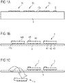
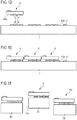
- a method for producing a lamp is specified. Furthermore, an illuminant is specified which can preferably be produced by means of the method.
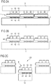
- the publication EP 1115155 describes an optical information processing device in which the contacting of each semiconductor body takes place by means of an uniquely assigned pair of connection points.
- At least one of the light-emitting diodes is connected to one of the CMOS chips, the upper side of the light-emitting diode being arranged on the upper side of the CMOS chip and each semiconductor body of the light-emitting diode being connected to a connection point of the CMOS chip.
- the upper side of the light-emitting diode and the CMOS chip face each other and the semiconductor bodies of the light-emitting diode are connected to corresponding connection points of the CMOS chip.
- the CMOS chip preferably has a number of connection points which corresponds at least to the number of semiconductor bodies of the light-emitting diode.
- a conversion element is applied to the radiation-transmissive carrier on the underside of the radiation-transmissive carrier facing away from the semiconductor bodies in such a way that electromagnetic radiation emitted by the semiconductor body passes through the conversion element during operation of the semiconductor body and is at least partially converted by the latter .
Landscapes
- Engineering & Computer Science (AREA)
- Microelectronics & Electronic Packaging (AREA)
- Physics & Mathematics (AREA)
- Condensed Matter Physics & Semiconductors (AREA)
- General Physics & Mathematics (AREA)
- Computer Hardware Design (AREA)
- Power Engineering (AREA)
- Led Device Packages (AREA)
- Led Devices (AREA)
Applications Claiming Priority (2)
| Application Number | Priority Date | Filing Date | Title |
|---|---|---|---|
| DE102009033915.9A DE102009033915B4 (de) | 2009-07-20 | 2009-07-20 | Verfahren zur Herstellung eines Leuchtmittels und Leuchtmittel |
| PCT/EP2010/060345 WO2011009821A1 (de) | 2009-07-20 | 2010-07-16 | Verfahren zur herstellung eines leuchtmittels und leuchtmittel |
Publications (2)
| Publication Number | Publication Date |
|---|---|
| EP2457254A1 EP2457254A1 (de) | 2012-05-30 |
| EP2457254B1 true EP2457254B1 (de) | 2020-03-18 |
Family
ID=43016842
Family Applications (1)
| Application Number | Title | Priority Date | Filing Date |
|---|---|---|---|
| EP10734486.3A Active EP2457254B1 (de) | 2009-07-20 | 2010-07-16 | Verfahren zur herstellung eines leuchtmittels und leuchtmittel |
Country Status (6)
| Country | Link |
|---|---|
| EP (1) | EP2457254B1 (enExample) |
| JP (1) | JP5813636B2 (enExample) |
| KR (1) | KR20120038511A (enExample) |
| CN (1) | CN102473704A (enExample) |
| DE (1) | DE102009033915B4 (enExample) |
| WO (1) | WO2011009821A1 (enExample) |
Families Citing this family (4)
| Publication number | Priority date | Publication date | Assignee | Title |
|---|---|---|---|---|
| DE102012202928A1 (de) * | 2012-02-27 | 2013-08-29 | Osram Gmbh | Lichtquelle mit led-chip und leuchtstoffschicht |
| DE102013205179A1 (de) * | 2013-03-25 | 2014-09-25 | Osram Gmbh | Verfahren zum Herstellen einer elektromagnetische Strahlung emittierenden Baugruppe und elektromagnetische Strahlung emittierende Baugruppe |
| GB201413578D0 (en) * | 2014-07-31 | 2014-09-17 | Infiniled Ltd | A colour iled display on silicon |
| KR102732448B1 (ko) | 2018-11-27 | 2024-11-21 | 삼성전자주식회사 | 마이크로 광원 어레이, 이를 포함한 디스플레이 장치 및 디스플레이 장치의 제조 방법 |
Family Cites Families (12)
| Publication number | Priority date | Publication date | Assignee | Title |
|---|---|---|---|---|
| US5940683A (en) * | 1996-01-18 | 1999-08-17 | Motorola, Inc. | LED display packaging with substrate removal and method of fabrication |
| JP3473396B2 (ja) * | 1998-04-23 | 2003-12-02 | 松下電器産業株式会社 | 光情報処理装置 |
| EP0977063A1 (en) * | 1998-07-28 | 2000-02-02 | Interuniversitair Micro-Elektronica Centrum Vzw | A socket and a system for optoelectronic interconnection and a method of fabricating such socket and system |
| JP3652945B2 (ja) * | 1999-12-28 | 2005-05-25 | 松下電器産業株式会社 | 光情報処理装置 |
| JP4182661B2 (ja) * | 2001-10-31 | 2008-11-19 | ソニー株式会社 | 画像表示装置及びその製造方法 |
| JP2005093649A (ja) * | 2003-09-17 | 2005-04-07 | Oki Data Corp | 半導体複合装置、ledプリントヘッド、及び、それを用いた画像形成装置 |
| US7294961B2 (en) * | 2004-03-29 | 2007-11-13 | Articulated Technologies, Llc | Photo-radiation source provided with emissive particles dispersed in a charge-transport matrix |
| CN1622730A (zh) * | 2004-12-16 | 2005-06-01 | 新磊微制造股份有限公司 | 发光模块 |
| TWI420691B (zh) | 2006-11-20 | 2013-12-21 | 尼康股份有限公司 | Led裝置及其製造方法 |
| DE102007010244A1 (de) * | 2007-02-02 | 2008-08-07 | Osram Opto Semiconductors Gmbh | Anordnung und Verfahren zur Erzeugung von Mischlicht |
| JP2008262993A (ja) * | 2007-04-10 | 2008-10-30 | Nikon Corp | 表示装置 |
| EP1988577B1 (en) * | 2007-04-30 | 2017-04-05 | Tridonic Jennersdorf GmbH | Light emitting diode module with silicon platform |
-
2009
- 2009-07-20 DE DE102009033915.9A patent/DE102009033915B4/de not_active Expired - Fee Related
-
2010
- 2010-07-16 EP EP10734486.3A patent/EP2457254B1/de active Active
- 2010-07-16 JP JP2012521009A patent/JP5813636B2/ja not_active Expired - Fee Related
- 2010-07-16 KR KR1020127004430A patent/KR20120038511A/ko not_active Withdrawn
- 2010-07-16 WO PCT/EP2010/060345 patent/WO2011009821A1/de not_active Ceased
- 2010-07-16 CN CN2010800331752A patent/CN102473704A/zh active Pending
Non-Patent Citations (1)
| Title |
|---|
| None * |
Also Published As
| Publication number | Publication date |
|---|---|
| DE102009033915A1 (de) | 2011-01-27 |
| CN102473704A (zh) | 2012-05-23 |
| JP5813636B2 (ja) | 2015-11-17 |
| KR20120038511A (ko) | 2012-04-23 |
| DE102009033915B4 (de) | 2022-05-25 |
| WO2011009821A1 (de) | 2011-01-27 |
| JP2012533895A (ja) | 2012-12-27 |
| EP2457254A1 (de) | 2012-05-30 |
Similar Documents
| Publication | Publication Date | Title |
|---|---|---|
| DE102015114849B4 (de) | Verfahren zur Herstellung von Leuchtdiodenfilamenten und Leuchtdiodenfilament | |
| WO2012160107A2 (de) | Optisches element, optoelektronisches bauelement und verfahren zur herstellung dieser | |
| DE102017106755B4 (de) | Verfahren zur Herstellung eines optoelektronischen Halbleiterbauteils und optoelektronisches Halbleiterbauteil | |
| WO2017202833A1 (de) | Filament und leuchtvorrichtung | |
| DE102008010512A1 (de) | Optoelektronisches Bauteil und Verfahren zur Herstellung eines optoelektronischen Bauteils | |
| EP2605895B1 (de) | Verfahren zur herstellung eines schichtverbunds aus einer lumineszenzkonversionsschicht und einer streuschicht | |
| WO2013139624A1 (de) | Optoelektronischer halbleiterchip und scheinwerfer mit einem solchen halbleiterchip | |
| DE102012213343A1 (de) | Optoelektronisches halbleiterbauteil mit saphir-flip-chip | |
| DE102012113003A1 (de) | Verfahren zur Herstellung eines optoelektronischen Halbleiterbauteils und optoelektronisches Halbleiterbauteil | |
| EP2845233B1 (de) | Led-modul | |
| EP2457254B1 (de) | Verfahren zur herstellung eines leuchtmittels und leuchtmittel | |
| DE102017100812A1 (de) | Verfahren zur Herstellung eines optoelektronischen Halbleiterbauteils und optoelektronisches Halbleiterbauteil | |
| DE102014105734A1 (de) | Optoelektronisches Halbleiterbauteil und Verfahren zur Herstellung eines optoelektronischen Halbleiterbauteils | |
| DE102016116000A1 (de) | Lichtemittierende Vorrichtung und Beleuchtungsvorrichtung | |
| DE102012200973A1 (de) | Leuchte und verfahren zur herstellung einer leuchte | |
| DE102016118996A1 (de) | Herstellung von sensoren | |
| WO2016023709A1 (de) | Beleuchtungsvorrichtung und verfahren zum herstellen einer solchen | |
| DE102014108362B4 (de) | Verfahren zur Herstellung mehrerer optoelektronischer Bauelemente und optoelektronisches Bauelement | |
| DE102015115812B4 (de) | Bauelement sowie Verfahren zur Herstellung eines Bauelements | |
| DE102009048401A1 (de) | Verfahren zum Herstellen eines optoelektronischen Halbleiterbauteils und optoelektronisches Halbleiterbauteil | |
| WO2009039846A1 (de) | Lichtemittierendes flächenelement und verfahren zum herstellen eines lichtemittierenden flächenelementes | |
| WO2015055646A2 (de) | Herstellung eines optoelektronischen bauelements | |
| DE102016125022A1 (de) | Herstellung von leuchtvorrichtungen | |
| DE102012007727A1 (de) | Festkörper-Leuchtmittelanordnung sowie Vorrichtung und Verfahren zu deren Herstellung | |
| DE102016103632A1 (de) | Bildpunkteeinheit und Videoanzeigeeinrichtung |
Legal Events
| Date | Code | Title | Description |
|---|---|---|---|
| PUAI | Public reference made under article 153(3) epc to a published international application that has entered the european phase |
Free format text: ORIGINAL CODE: 0009012 |
|
| 17P | Request for examination filed |
Effective date: 20111109 |
|
| AK | Designated contracting states |
Kind code of ref document: A1 Designated state(s): AL AT BE BG CH CY CZ DE DK EE ES FI FR GB GR HR HU IE IS IT LI LT LU LV MC MK MT NL NO PL PT RO SE SI SK SM TR |
|
| DAX | Request for extension of the european patent (deleted) | ||
| STAA | Information on the status of an ep patent application or granted ep patent |
Free format text: STATUS: EXAMINATION IS IN PROGRESS |
|
| 17Q | First examination report despatched |
Effective date: 20180518 |
|
| RAP1 | Party data changed (applicant data changed or rights of an application transferred) |
Owner name: OSRAM OPTO SEMICONDUCTORS GMBH |
|
| GRAP | Despatch of communication of intention to grant a patent |
Free format text: ORIGINAL CODE: EPIDOSNIGR1 |
|
| STAA | Information on the status of an ep patent application or granted ep patent |
Free format text: STATUS: GRANT OF PATENT IS INTENDED |
|
| INTG | Intention to grant announced |
Effective date: 20191112 |
|
| GRAS | Grant fee paid |
Free format text: ORIGINAL CODE: EPIDOSNIGR3 |
|
| GRAA | (expected) grant |
Free format text: ORIGINAL CODE: 0009210 |
|
| STAA | Information on the status of an ep patent application or granted ep patent |
Free format text: STATUS: THE PATENT HAS BEEN GRANTED |
|
| AK | Designated contracting states |
Kind code of ref document: B1 Designated state(s): AL AT BE BG CH CY CZ DE DK EE ES FI FR GB GR HR HU IE IS IT LI LT LU LV MC MK MT NL NO PL PT RO SE SI SK SM TR |
|
| REG | Reference to a national code |
Ref country code: GB Ref legal event code: FG4D Free format text: NOT ENGLISH |
|
| REG | Reference to a national code |
Ref country code: DE Ref legal event code: R096 Ref document number: 502010016537 Country of ref document: DE |
|
| REG | Reference to a national code |
Ref country code: AT Ref legal event code: REF Ref document number: 1246908 Country of ref document: AT Kind code of ref document: T Effective date: 20200415 Ref country code: IE Ref legal event code: FG4D Free format text: LANGUAGE OF EP DOCUMENT: GERMAN |
|
| PG25 | Lapsed in a contracting state [announced via postgrant information from national office to epo] |
Ref country code: FI Free format text: LAPSE BECAUSE OF FAILURE TO SUBMIT A TRANSLATION OF THE DESCRIPTION OR TO PAY THE FEE WITHIN THE PRESCRIBED TIME-LIMIT Effective date: 20200318 Ref country code: NO Free format text: LAPSE BECAUSE OF FAILURE TO SUBMIT A TRANSLATION OF THE DESCRIPTION OR TO PAY THE FEE WITHIN THE PRESCRIBED TIME-LIMIT Effective date: 20200618 |
|
| REG | Reference to a national code |
Ref country code: NL Ref legal event code: MP Effective date: 20200318 |
|
| PG25 | Lapsed in a contracting state [announced via postgrant information from national office to epo] |
Ref country code: GR Free format text: LAPSE BECAUSE OF FAILURE TO SUBMIT A TRANSLATION OF THE DESCRIPTION OR TO PAY THE FEE WITHIN THE PRESCRIBED TIME-LIMIT Effective date: 20200619 Ref country code: BG Free format text: LAPSE BECAUSE OF FAILURE TO SUBMIT A TRANSLATION OF THE DESCRIPTION OR TO PAY THE FEE WITHIN THE PRESCRIBED TIME-LIMIT Effective date: 20200618 Ref country code: LV Free format text: LAPSE BECAUSE OF FAILURE TO SUBMIT A TRANSLATION OF THE DESCRIPTION OR TO PAY THE FEE WITHIN THE PRESCRIBED TIME-LIMIT Effective date: 20200318 Ref country code: SE Free format text: LAPSE BECAUSE OF FAILURE TO SUBMIT A TRANSLATION OF THE DESCRIPTION OR TO PAY THE FEE WITHIN THE PRESCRIBED TIME-LIMIT Effective date: 20200318 Ref country code: HR Free format text: LAPSE BECAUSE OF FAILURE TO SUBMIT A TRANSLATION OF THE DESCRIPTION OR TO PAY THE FEE WITHIN THE PRESCRIBED TIME-LIMIT Effective date: 20200318 |
|
| REG | Reference to a national code |
Ref country code: LT Ref legal event code: MG4D |
|
| PG25 | Lapsed in a contracting state [announced via postgrant information from national office to epo] |
Ref country code: NL Free format text: LAPSE BECAUSE OF FAILURE TO SUBMIT A TRANSLATION OF THE DESCRIPTION OR TO PAY THE FEE WITHIN THE PRESCRIBED TIME-LIMIT Effective date: 20200318 |
|
| PG25 | Lapsed in a contracting state [announced via postgrant information from national office to epo] |
Ref country code: IS Free format text: LAPSE BECAUSE OF FAILURE TO SUBMIT A TRANSLATION OF THE DESCRIPTION OR TO PAY THE FEE WITHIN THE PRESCRIBED TIME-LIMIT Effective date: 20200718 Ref country code: SK Free format text: LAPSE BECAUSE OF FAILURE TO SUBMIT A TRANSLATION OF THE DESCRIPTION OR TO PAY THE FEE WITHIN THE PRESCRIBED TIME-LIMIT Effective date: 20200318 Ref country code: SM Free format text: LAPSE BECAUSE OF FAILURE TO SUBMIT A TRANSLATION OF THE DESCRIPTION OR TO PAY THE FEE WITHIN THE PRESCRIBED TIME-LIMIT Effective date: 20200318 Ref country code: PT Free format text: LAPSE BECAUSE OF FAILURE TO SUBMIT A TRANSLATION OF THE DESCRIPTION OR TO PAY THE FEE WITHIN THE PRESCRIBED TIME-LIMIT Effective date: 20200812 Ref country code: EE Free format text: LAPSE BECAUSE OF FAILURE TO SUBMIT A TRANSLATION OF THE DESCRIPTION OR TO PAY THE FEE WITHIN THE PRESCRIBED TIME-LIMIT Effective date: 20200318 Ref country code: RO Free format text: LAPSE BECAUSE OF FAILURE TO SUBMIT A TRANSLATION OF THE DESCRIPTION OR TO PAY THE FEE WITHIN THE PRESCRIBED TIME-LIMIT Effective date: 20200318 Ref country code: LT Free format text: LAPSE BECAUSE OF FAILURE TO SUBMIT A TRANSLATION OF THE DESCRIPTION OR TO PAY THE FEE WITHIN THE PRESCRIBED TIME-LIMIT Effective date: 20200318 Ref country code: CZ Free format text: LAPSE BECAUSE OF FAILURE TO SUBMIT A TRANSLATION OF THE DESCRIPTION OR TO PAY THE FEE WITHIN THE PRESCRIBED TIME-LIMIT Effective date: 20200318 |
|
| REG | Reference to a national code |
Ref country code: DE Ref legal event code: R097 Ref document number: 502010016537 Country of ref document: DE |
|
| PLBE | No opposition filed within time limit |
Free format text: ORIGINAL CODE: 0009261 |
|
| STAA | Information on the status of an ep patent application or granted ep patent |
Free format text: STATUS: NO OPPOSITION FILED WITHIN TIME LIMIT |
|
| PG25 | Lapsed in a contracting state [announced via postgrant information from national office to epo] |
Ref country code: IT Free format text: LAPSE BECAUSE OF FAILURE TO SUBMIT A TRANSLATION OF THE DESCRIPTION OR TO PAY THE FEE WITHIN THE PRESCRIBED TIME-LIMIT Effective date: 20200318 Ref country code: DK Free format text: LAPSE BECAUSE OF FAILURE TO SUBMIT A TRANSLATION OF THE DESCRIPTION OR TO PAY THE FEE WITHIN THE PRESCRIBED TIME-LIMIT Effective date: 20200318 Ref country code: ES Free format text: LAPSE BECAUSE OF FAILURE TO SUBMIT A TRANSLATION OF THE DESCRIPTION OR TO PAY THE FEE WITHIN THE PRESCRIBED TIME-LIMIT Effective date: 20200318 |
|
| 26N | No opposition filed |
Effective date: 20201221 |
|
| PG25 | Lapsed in a contracting state [announced via postgrant information from national office to epo] |
Ref country code: PL Free format text: LAPSE BECAUSE OF FAILURE TO SUBMIT A TRANSLATION OF THE DESCRIPTION OR TO PAY THE FEE WITHIN THE PRESCRIBED TIME-LIMIT Effective date: 20200318 Ref country code: MC Free format text: LAPSE BECAUSE OF FAILURE TO SUBMIT A TRANSLATION OF THE DESCRIPTION OR TO PAY THE FEE WITHIN THE PRESCRIBED TIME-LIMIT Effective date: 20200318 |
|
| REG | Reference to a national code |
Ref country code: CH Ref legal event code: PL |
|
| GBPC | Gb: european patent ceased through non-payment of renewal fee |
Effective date: 20200716 |
|
| REG | Reference to a national code |
Ref country code: BE Ref legal event code: MM Effective date: 20200731 |
|
| PG25 | Lapsed in a contracting state [announced via postgrant information from national office to epo] |
Ref country code: LU Free format text: LAPSE BECAUSE OF NON-PAYMENT OF DUE FEES Effective date: 20200716 Ref country code: GB Free format text: LAPSE BECAUSE OF NON-PAYMENT OF DUE FEES Effective date: 20200716 Ref country code: FR Free format text: LAPSE BECAUSE OF NON-PAYMENT OF DUE FEES Effective date: 20200731 Ref country code: CH Free format text: LAPSE BECAUSE OF NON-PAYMENT OF DUE FEES Effective date: 20200731 Ref country code: LI Free format text: LAPSE BECAUSE OF NON-PAYMENT OF DUE FEES Effective date: 20200731 |
|
| PG25 | Lapsed in a contracting state [announced via postgrant information from national office to epo] |
Ref country code: BE Free format text: LAPSE BECAUSE OF NON-PAYMENT OF DUE FEES Effective date: 20200731 Ref country code: SI Free format text: LAPSE BECAUSE OF FAILURE TO SUBMIT A TRANSLATION OF THE DESCRIPTION OR TO PAY THE FEE WITHIN THE PRESCRIBED TIME-LIMIT Effective date: 20200318 |
|
| PG25 | Lapsed in a contracting state [announced via postgrant information from national office to epo] |
Ref country code: IE Free format text: LAPSE BECAUSE OF NON-PAYMENT OF DUE FEES Effective date: 20200716 |
|
| REG | Reference to a national code |
Ref country code: AT Ref legal event code: MM01 Ref document number: 1246908 Country of ref document: AT Kind code of ref document: T Effective date: 20200716 |
|
| PG25 | Lapsed in a contracting state [announced via postgrant information from national office to epo] |
Ref country code: AT Free format text: LAPSE BECAUSE OF NON-PAYMENT OF DUE FEES Effective date: 20200716 |
|
| PGFP | Annual fee paid to national office [announced via postgrant information from national office to epo] |
Ref country code: DE Payment date: 20210721 Year of fee payment: 12 |
|
| PG25 | Lapsed in a contracting state [announced via postgrant information from national office to epo] |
Ref country code: TR Free format text: LAPSE BECAUSE OF FAILURE TO SUBMIT A TRANSLATION OF THE DESCRIPTION OR TO PAY THE FEE WITHIN THE PRESCRIBED TIME-LIMIT Effective date: 20200318 Ref country code: MT Free format text: LAPSE BECAUSE OF FAILURE TO SUBMIT A TRANSLATION OF THE DESCRIPTION OR TO PAY THE FEE WITHIN THE PRESCRIBED TIME-LIMIT Effective date: 20200318 Ref country code: CY Free format text: LAPSE BECAUSE OF FAILURE TO SUBMIT A TRANSLATION OF THE DESCRIPTION OR TO PAY THE FEE WITHIN THE PRESCRIBED TIME-LIMIT Effective date: 20200318 |
|
| PG25 | Lapsed in a contracting state [announced via postgrant information from national office to epo] |
Ref country code: MK Free format text: LAPSE BECAUSE OF FAILURE TO SUBMIT A TRANSLATION OF THE DESCRIPTION OR TO PAY THE FEE WITHIN THE PRESCRIBED TIME-LIMIT Effective date: 20200318 Ref country code: AL Free format text: LAPSE BECAUSE OF FAILURE TO SUBMIT A TRANSLATION OF THE DESCRIPTION OR TO PAY THE FEE WITHIN THE PRESCRIBED TIME-LIMIT Effective date: 20200318 |
|
| REG | Reference to a national code |
Ref country code: DE Ref legal event code: R119 Ref document number: 502010016537 Country of ref document: DE |
|
| PG25 | Lapsed in a contracting state [announced via postgrant information from national office to epo] |
Ref country code: DE Free format text: LAPSE BECAUSE OF NON-PAYMENT OF DUE FEES Effective date: 20230201 |