EP2456005A1 - Signal line and circuit board - Google Patents
Signal line and circuit board Download PDFInfo
- Publication number
- EP2456005A1 EP2456005A1 EP10799720A EP10799720A EP2456005A1 EP 2456005 A1 EP2456005 A1 EP 2456005A1 EP 10799720 A EP10799720 A EP 10799720A EP 10799720 A EP10799720 A EP 10799720A EP 2456005 A1 EP2456005 A1 EP 2456005A1
- Authority
- EP
- European Patent Office
- Prior art keywords
- signal line
- axis direction
- ground conductor
- via hole
- ground
- Prior art date
- Legal status (The legal status is an assumption and is not a legal conclusion. Google has not performed a legal analysis and makes no representation as to the accuracy of the status listed.)
- Granted
Links
Images


Classifications
-
- H—ELECTRICITY
- H05—ELECTRIC TECHNIQUES NOT OTHERWISE PROVIDED FOR
- H05K—PRINTED CIRCUITS; CASINGS OR CONSTRUCTIONAL DETAILS OF ELECTRIC APPARATUS; MANUFACTURE OF ASSEMBLAGES OF ELECTRICAL COMPONENTS
- H05K1/00—Printed circuits
- H05K1/02—Details
- H05K1/0296—Conductive pattern lay-out details not covered by sub groups H05K1/02 - H05K1/0295
- H05K1/0298—Multilayer circuits
-
- H—ELECTRICITY
- H01—ELECTRIC ELEMENTS
- H01P—WAVEGUIDES; RESONATORS, LINES, OR OTHER DEVICES OF THE WAVEGUIDE TYPE
- H01P3/00—Waveguides; Transmission lines of the waveguide type
- H01P3/02—Waveguides; Transmission lines of the waveguide type with two longitudinal conductors
- H01P3/08—Microstrips; Strip lines
-
- H—ELECTRICITY
- H01—ELECTRIC ELEMENTS
- H01P—WAVEGUIDES; RESONATORS, LINES, OR OTHER DEVICES OF THE WAVEGUIDE TYPE
- H01P3/00—Waveguides; Transmission lines of the waveguide type
- H01P3/02—Waveguides; Transmission lines of the waveguide type with two longitudinal conductors
- H01P3/08—Microstrips; Strip lines
- H01P3/081—Microstriplines
-
- H—ELECTRICITY
- H01—ELECTRIC ELEMENTS
- H01P—WAVEGUIDES; RESONATORS, LINES, OR OTHER DEVICES OF THE WAVEGUIDE TYPE
- H01P3/00—Waveguides; Transmission lines of the waveguide type
- H01P3/02—Waveguides; Transmission lines of the waveguide type with two longitudinal conductors
- H01P3/08—Microstrips; Strip lines
- H01P3/088—Stacked transmission lines
-
- H—ELECTRICITY
- H05—ELECTRIC TECHNIQUES NOT OTHERWISE PROVIDED FOR
- H05K—PRINTED CIRCUITS; CASINGS OR CONSTRUCTIONAL DETAILS OF ELECTRIC APPARATUS; MANUFACTURE OF ASSEMBLAGES OF ELECTRICAL COMPONENTS
- H05K1/00—Printed circuits
- H05K1/02—Details
- H05K1/0213—Electrical arrangements not otherwise provided for
- H05K1/0216—Reduction of cross-talk, noise or electromagnetic interference
- H05K1/0218—Reduction of cross-talk, noise or electromagnetic interference by printed shielding conductors, ground planes or power plane
- H05K1/0219—Printed shielding conductors for shielding around or between signal conductors, e.g. coplanar or coaxial printed shielding conductors
-
- H—ELECTRICITY
- H05—ELECTRIC TECHNIQUES NOT OTHERWISE PROVIDED FOR
- H05K—PRINTED CIRCUITS; CASINGS OR CONSTRUCTIONAL DETAILS OF ELECTRIC APPARATUS; MANUFACTURE OF ASSEMBLAGES OF ELECTRICAL COMPONENTS
- H05K1/00—Printed circuits
- H05K1/02—Details
- H05K1/0277—Bendability or stretchability details
- H05K1/028—Bending or folding regions of flexible printed circuits
-
- H—ELECTRICITY
- H05—ELECTRIC TECHNIQUES NOT OTHERWISE PROVIDED FOR
- H05K—PRINTED CIRCUITS; CASINGS OR CONSTRUCTIONAL DETAILS OF ELECTRIC APPARATUS; MANUFACTURE OF ASSEMBLAGES OF ELECTRICAL COMPONENTS
- H05K3/00—Apparatus or processes for manufacturing printed circuits
- H05K3/46—Manufacturing multilayer circuits
-
- H—ELECTRICITY
- H05—ELECTRIC TECHNIQUES NOT OTHERWISE PROVIDED FOR
- H05K—PRINTED CIRCUITS; CASINGS OR CONSTRUCTIONAL DETAILS OF ELECTRIC APPARATUS; MANUFACTURE OF ASSEMBLAGES OF ELECTRICAL COMPONENTS
- H05K1/00—Printed circuits
- H05K1/02—Details
- H05K1/0213—Electrical arrangements not otherwise provided for
- H05K1/0216—Reduction of cross-talk, noise or electromagnetic interference
- H05K1/0218—Reduction of cross-talk, noise or electromagnetic interference by printed shielding conductors, ground planes or power plane
- H05K1/0224—Patterned shielding planes, ground planes or power planes
- H05K1/0225—Single or multiple openings in a shielding, ground or power plane
-
- H—ELECTRICITY
- H05—ELECTRIC TECHNIQUES NOT OTHERWISE PROVIDED FOR
- H05K—PRINTED CIRCUITS; CASINGS OR CONSTRUCTIONAL DETAILS OF ELECTRIC APPARATUS; MANUFACTURE OF ASSEMBLAGES OF ELECTRICAL COMPONENTS
- H05K2201/00—Indexing scheme relating to printed circuits covered by H05K1/00
- H05K2201/07—Electric details
- H05K2201/0707—Shielding
- H05K2201/0715—Shielding provided by an outer layer of PCB
-
- H—ELECTRICITY
- H05—ELECTRIC TECHNIQUES NOT OTHERWISE PROVIDED FOR
- H05K—PRINTED CIRCUITS; CASINGS OR CONSTRUCTIONAL DETAILS OF ELECTRIC APPARATUS; MANUFACTURE OF ASSEMBLAGES OF ELECTRICAL COMPONENTS
- H05K2201/00—Indexing scheme relating to printed circuits covered by H05K1/00
- H05K2201/09—Shape and layout
- H05K2201/09209—Shape and layout details of conductors
- H05K2201/095—Conductive through-holes or vias
- H05K2201/09618—Via fence, i.e. one-dimensional array of vias
Definitions
- the present invention relates to a signal line and the circuit substrate thereof, and, more specifically, relates to a signal line, inflected and used, and the circuit substrate thereof.
- a flexible substrate described in PTL 1 has been known.
- Fig. 5 is the cross-section structure diagram of a flexible substrate 500 described in PTL 1.
- a cross-section structure illustrated in Fig. 5(a) and a cross-section structure illustrated in Fig. 5(b) are alternately disposed, and hence the flexible substrate 500 is configured. More specifically, the flexible substrate 500 includes insulation layers 502a to 502d, a signal line 504 and ground layers 506a and 506b. Insulation layers 502a to 502d are sheets including flexible material and laminated. The signal line 504 is provided on the insulation layer 502c, and extends parallel to the vertical direction of the plane of paper of Fig. 5(a) .
- the ground layer 506a is provided on the insulation layer 502b, and located above the signal line 504 in a lamination direction.
- the ground layer 506b is provided on the insulation layer 502d, and located below the signal line 504 in the lamination direction.
- the ground layers 506a and 506b overlap with the signal line 504 in the lamination direction.
- the ground layers 506a and 506b do not overlap with the signal line 504 in the lamination direction. Namely, opening portions 508a and 508b are provided in the ground layers 506a and 506b, respectively.
- Such a flexible substrate 500 as described above is easy to inflect and use, as described below. More specifically, since the ground layers 506a and 506b are configured using metal foil or the like, it is hard for the ground layers 506a and 506b to expand and contract compared with the insulation layers 502a to 502d. Therefore, as illustrated in Fig. 5(b) , in the flexible substrate 500, the opening portions 508a and 508b are provided in the ground layers 506a and 506b. Accordingly, in a portion illustrated in Fig. 5(b) , since the widths of the ground layers 506a and 506b become small, it is easy for the ground layers 506a and 506b to expand and contract. As a result, it is possible to easily bend the flexible substrate 500.
- the flexible substrate 500 has a problem that unnecessary radiation from the signal line 504 occurs. More specifically, the opening portions 508a and 508b are provided in the ground layers 506a and 506b. Therefore, in planar view form the lamination direction, the signal line 504 is exposed through the opening portions 508a and 508b. As a result, unnecessary radiation to be fundamentally absorbed by the ground layers 506a and 506b leaks to the outside of the flexible substrate 500 through the opening portions 508a and 508b.
- an object of the present invention is to provide a signal line and a circuit substrate, which are capable of being easily inflected and reducing unnecessary radiation.
- a signal line according to a first embodiment of the present invention includes a laminated body including a plurality of insulator layers that include flexible material and are laminated; a linear signal line provided within the laminated body; a first ground conductor located above the signal line in a lamination direction within the laminated body and overlapping with the signal line in planar view from the lamination direction; a second ground conductor located below the signal line in the lamination direction within the laminated body and overlapping with the signal line in planar view from the lamination direction; and a via hole conductor connecting the first ground conductor and the second ground conductor to each other, wherein in the first ground conductor, a plurality of first opening portions are provided so as to be arranged along the signal line in planar view from the lamination direction, and in planar view from the lamination direction, the via hole conductor is provided between the first opening portions adjacent to each other, in a direction in which the signal line extends.
- a circuit substrate includes a main body including a plurality of insulator layers that include flexible material and are laminated and including a first circuit portion, a second circuit portion, and a signal line portion; a linear signal line provided within the signal line portion; a first ground conductor located above the signal line in a lamination direction within the signal line portion and overlapping with the signal line in planar view from the lamination direction; a second ground conductor located below the signal line in the lamination direction within the signal line portion and overlapping with the signal line in planar view from the lamination direction; and a via hole conductor connecting the first ground conductor and the second ground conductor to each other, wherein in the first ground conductor, a plurality of first opening portions are provided so as to be arranged along the signal line in planar view from the lamination direction, in planar view from the lamination direction, the via hole conductor is provided between the first opening portions adjacent to each other, in a direction in which the signal line extends, and the first circuit portion and the second
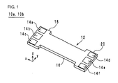
- Fig. 1 is the external appearance perspective view of a signal line 10a, 10b according to an embodiment of the present invention.
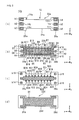
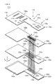
- Fig. 2 is the exploded view of the signal line 10a in Fig. 1 .
- the lamination direction of the signal line 10a is defined as a z axis direction.
- the longitudinal direction of the signal line 10a is defined as an x axis direction, and a direction perpendicular to the x axis direction and the z axis direction is defined as a y axis direction.
- the signal line 10a connects two circuit substrates to each other in an electronic device such as a mobile phone or the like.
- the signal line 10a includes a laminated body 12, external terminals 14 (14a to 14f), ground conductors 30 and 34, a signal line 32, and via hole conductors b1 to b16 and B1 to B36.
- the laminated body 12 includes a signal line portion 16 and connector portions 18 and 20.
- the signal line portion 16 extends in the x axis direction, and contains the signal line 32 and the ground conductors 30 and 34.
- the signal line portion 16 is configured so as to be able to be bent into a U shape.
- the connector portions 18 and 20 are provided at both ends of the signal line portion 16 in the x axis direction, and connected to the connectors of the circuit substrates not illustrated.
- Insulation sheets (insulator layers) 22 (22a to 22d) illustrated in Fig. 2 are laminated from the positive direction side of the z axis direction to the negative direction side thereof in this order, thereby configuring the laminated body 12.
- the insulation sheet 22 is configured using thermoplastic resin such as liquid crystalline polymer having flexibility, or the like. As illustrated in Fig. 2 , the insulation sheets 22a to 22d are configured using signal line portions 24a to 24d, connector portions 26a to 26d, and connector portions 28a to 28d, respectively.
- the signal line portion 24 configures the signal line portion 16 of the laminated body 12
- the connector portions 26 and 28 configure the connector portions 18 and 20 of the laminated body 12, respectively.
- a main surface on a positive direction side in the z axis direction of the insulation sheet 22 is referred to as a front surface
- a main surface on a negative direction side in the z axis direction of the insulation sheet 22 is referred to as a back surface.
- the external terminals 14a to 14c are provided so as to form a line in the y axis direction on the front surface of the connector portion 26a.
- the external terminals 14a to 14c are in contact with terminals within the connector.
- the external terminals 14a and 14c are in contact with ground terminals within the connector, and the external terminal 14b is in contact with a signal terminal within the connector. Accordingly, a ground potential is applied to the external terminals 14a and 14c, and a highfrequency signal (for example, 2 GHz) is applied to the external terminal 14b.
- the external terminals 14d to 14f are provided so as to form a line in the y axis direction on the front surface of the connector portion 28a.
- the external terminals 14d to 14f are in contact with terminals within the connector.
- the external terminals 14d and 14f are in contact with ground terminals within the connector, and the external terminal 14e is in contact with a signal terminal within the connector. Accordingly, a ground potential is applied to the external terminals 14d and 14f, and a highfrequency signal (for example, 2 GHz) is applied to the external terminal 14e.
- the signal line 32 is a linear conductor provided within the laminated body 12, and is provided on the front surface of the insulation sheet 22c.
- the signal line 32 extends in the x axis direction on the front surface of the insulation sheet 24c.
- both ends of the signal line 32 are located at the connector portions 26c and 28c, respectively.
- the ground conductor 30 is provided on a positive direction side in the z axis direction within the laminated body 12, compared with the signal line 32, and more specifically, is provided on the front surface of the insulation sheet 22b.
- the ground conductor 30 extends in the x axis direction on the front surface of the signal line portion 24b.
- One end of the ground conductor 30 is situated in a state in which the end thereof branches into two portions in the connector portion 26b, and the other end of the ground conductor 30 is situated in a state in which the end thereof branches into two portions in the connector portion 28b.
- the ground conductor 30 overlaps with the signal line 32 in planar view from the z axis direction.
- a plurality of slit-shaped opening portions O1 to O8 in which no conductor is provided are provided so as to be arranged along the signal line 32 in planar view from the z axis direction.
- the opening portions O1 to 08 overlap with the signal line 32 in planar view from the z axis direction.
- the opening portions O1 to 08 have rectangle shapes whose longitudinal directions correspond to the y axis direction, and form a line in the x axis direction at regular intervals.
- the openings O1 to 08 are provided so as not to segmentalize the ground conductor 30.
- the conductor of the ground conductor 30 exists on the positive direction side and the negative direction side of the openings O1 to 08 in the y axis direction. Accordingly, the ground conductor 30 forms a ladder shape.
- the openings O1 to O8 are provided in the ground conductor 30, and hence, as illustrated in Fig. 2 , in the ground conductor 30, a relatively thick portion and a relatively thin portion are provided in width in the y axis direction.
- the ground conductor 34 is provided on a negative direction side in the z axis direction within the laminated body 12, compared with the signal line 32, and more specifically, is provided on the front surface of the insulation sheet 22d.
- the ground conductor 34 extends in the x axis direction on the front surface of the signal line portion 24d.
- One end of the ground conductor 34 is situated in a state in which the end thereof branches into two portions in the connector portion 26d, and the other end of the ground conductor 34 is situated in a state in which the end thereof branches into two portions in the connector portion 28d.
- the ground conductor 34 overlaps with the signal line 32 in planar view from the z axis direction.
- a plurality of slit-shaped opening portions O11 to 018 in which no conductor is provided are provided so as to be arranged along the signal line 32 in planar view from the z axis direction.
- the opening portions O11 to 018 overlap with the signal line 32 in planar view from the z axis direction.
- the opening portions O11 to 018 overlap with the opening portions O1 to 08, respectively, in a state in which the opening portions O11 to 018 coincide with the opening portions O1 to 08, respectively.
- the opening portions O11 to 018 have rectangle shapes whose longitudinal directions correspond to the y axis direction, and form a line in the x axis direction at regular intervals.
- the opening portions O11 to 018 are provided so as not to segmentalize the ground conductor 34.
- the conductor of the ground conductor 34 exists on the positive direction side and the negative direction side of the openings O11 to 018 in the y axis direction. Accordingly, the ground conductor 34 forms a ladder shape.
- the openings O11 to 018 are provided in the ground conductor 34, and hence, as illustrated in Fig. 2 , in the ground conductor 34, a relatively thick portion and a relatively thin portion are provided in width in the y axis direction.
- the via hole conductors b1 and b3 are provided so as to penetrate through the connector portion 26a in the z axis direction, and connect the external terminals 14a and 14c to the ground conductor 30, respectively.
- the via hole conductor b2 is provided so as to penetrate through the connector portion 26a in the z axis direction, and is connected to the external terminal 14b.
- each of the via hole conductors b7 and b9 is provided so as to penetrate through the connector portion 26b in the z axis direction, and is connected to the ground conductor 30.
- the via hole conductor b8 is provided so as to penetrate through the connector portion 26b in the z axis direction, and connects the via hole conductor b2 and the signal line 32 to each other.
- the via hole conductors b13 and b14 are provided so as to penetrate through the connector portion 26c in the z axis direction, and connect the via hole conductors b7 and b9 to the ground conductor 34, respectively.
- the external terminal 14a is connected to the ground conductors 30 and 34 through the via hole conductors b1, b7, and b13
- the external terminal 14c is connected to the ground conductors 30 and 34 through the via hole conductors b3, b9, and b14.
- the external terminal 14b and the signal line 32 are connected to each other through the via hole conductors b2 and b8.
- the via hole conductors b4 and b6 are provided so as to penetrate through the connector portion 28a in the z axis direction, and connect the external terminals 14d and 14f to the ground conductor 30, respectively.
- the via hole conductor b5 is provided so as to penetrate through the connector portion 28a in the z axis direction, and is connected to the external terminal 14e.
- each of the via hole conductors b10 and b12 is provided so as to penetrate through the connector portion 28b in the z axis direction, and is connected to the ground conductor 30.
- the via hole conductor b11 is provided so as to penetrate through the connector portion 28b in the z axis direction, and connects the via hole conductor b5 and the signal line 32 to each other.
- the via hole conductors b15 and b16 are provided so as to penetrate through the connector portion 28c in the z axis direction, and connect the via hole conductors b10 and b12 to the ground conductor 34, respectively.
- the external terminal 14d is connected to the ground conductors 30 and 34 through the via hole conductors b4, b10, and b15
- the external terminal 14f is connected to the ground conductors 30 and 34 through the via hole conductors b6, b12, and b16.
- the external terminal 14e and the signal line 32 are connected to each other through the via hole conductors b5 and b11.
- the via hole conductors B1 to B18 and the via hole conductors B19 to B36 are provided so as to penetrate through the signal line portions 24b and 24c in the z axis direction, respectively, and connect the ground conductor 30 and the ground conductor 34 to each other. Furthermore, in planar view from the z axis direction, the via hole conductors B1 to B18 are provided between the opening portions O1 to O8 adjacent to one another, in a direction (namely, the x axis direction) in which the signal line 32 extends.
- the via hole conductors B1, B3, B5, B7, B9, B11, B13, B15, and B17 are provided so as to lie on a straight line in the x axis direction with being equally spaced.
- the via hole conductors B2, B4, B6, B8, B10, B12, B14, B16, and B18 are provided so as to lie on a straight line in the x axis direction with being equally spaced.
- the via hole conductors B3 to B16 are provided on perpendicular bisectors with respect to the centers of the opening portions O1 to O8 adjacent to one another.
- the via hole conductors B3 and B4 will be described as an example.
- the via hole conductors B3 and B4 are provided between the opening portion O1 and the opening portion 02.
- the points of intersection between the diagonal lines of the opening portions O1 and 02 are referred to as the centers P1 and P2 of the opening portions O1 and 02.
- the perpendicular bisector of the centers P1 and P2 is referred to as a straight line L1.
- the via hole conductor B3 is located on the straight line L1, and is provided so as to overlap with end portions on the positive direction sides of the openings O1 to 08 in the y axis direction in planar view from the x axis direction.
- the via hole conductor B4 is located on the straight line L1, and is provided so as to overlap with end portions on the negative direction sides of the openings O1 to 08 in the y axis direction in planar view from the x axis direction.
- the via hole conductors B19 to B36 are provided in the signal line portion 24c so as to overlap with the via hole conductors B1 to B18, respectively, in planar view from the z axis direction. Accordingly, the via hole conductors B19 to B36 are connected to the via hole conductors B1 to B18, respectively.
- the insulation sheets 22a to 22d having the above-mentioned configurations are laminated, and hence the ground conductors 30 and 34 and the signal line 32 form a stripline structure.
- the signal line 32 is sandwiched in between the ground conductor 30 and the ground conductor 34 in the z axis direction, and is housed within a region in which the ground conductors 30 and 34 are provided, in planar view from the z axis direction.
- the ground conductor 30 and the ground conductor 34 are connected to each other using the via hole conductors B1 to B36.
- the signal line 10a having the above-mentioned configuration is used in a state in which the signal line 10a is inflected. Namely, in planar view from the y axis direction, the signal line 10a is inflected so as to form a U shape protruding toward one of a positive direction side and a negative direction side in the z axis direction.
- a manufacturing method for the signal line 10a will be described with reference to Fig. 2 . While, hereinafter, a case in which one signal line 10a is manufactured will be described as an example, actually, large-sized insulation sheets are laminated and cut, thereby simultaneously manufacturing a plurality of the signal lines 10a.
- the insulation sheet 22 is prepared where copper foil is formed on the whole surface of the front surface.
- the front surface of the copper foil of the insulation sheet 22 is plated with zinc for antirust effect, thereby being smoothed.
- the external terminal 14 illustrated in Fig. 2 is formed on the front surface of the insulation sheet 22a.
- resist having the same shape as the external terminal 14 illustrated in Fig. 2 is printed.
- the copper foil is subjected to etching processing, thereby removing the copper foil of a portion not covered with the resist. After that, the resist is removed. Accordingly, such an external terminal 14 as illustrated in Fig. 2 is formed on the front surface of the insulation sheet 22a.
- the ground conductor 30 illustrated in Fig. 2 is formed on the front surface of the insulation sheet 22b.
- the signal line 32 illustrated in Fig. 2 is formed on the front surface of the insulation sheet 22c.
- the ground conductor 34 illustrated in Fig. 2 is formed on the front surface of the insulation sheet 22d.
- these photolithography processes are the same as the photolithography process performed when the external terminal 14 is formed, the descriptions thereof will be omitted. Owing to the above-mentioned processes, the insulation sheets 22b and 22d, to the front surfaces of which the ground conductors 30 and 34 adhere, and the insulation sheet 22c, to the front surface of which the signal line 32 adheres, are prepared.
- positions at which the via hole conductors b1 to b16 and B1 to B36 of the insulation sheets 22a to 22c are to be formed are irradiated with a laser beam from a back surface side, thereby forming via holes.
- via holes formed in the insulation sheets 22a to 22c are filled with conductive paste whose main component is copper, there by forming the via hole conductors b1 to b16 and B1 to B36 illustrated in Fig. 2 .
- the insulation sheets 22a to 22d are stacked from a positive direction side in the z axis direction to a negative direction side therein in this order so that the ground conductor 30, the signal line 32, and the ground conductor 34 form a stripline structure.
- the insulation sheets 22a to 22d are fixed. Accordingly, the signal line 10a illustrated in Fig. 1 is obtained.
- the ground conductors 30 and 34 are configured using metal foil or the like, it is hard for the ground conductors 30 and 34 to expand and contract compared with the insulation layers 22a to 22d. Therefore, in the signal line 10a, as illustrated in Fig. 2 , the opening portions O1 to 08 and O11 to 018 are provided in the ground conductors 30 and 34. Accordingly, the strengths of the ground conductors 30 and 34 in portions in which the opening portions O1 to 08 and O11 to 018 are provided become lower than the strengths of the ground conductors 30 and 34 in other portions.
- the ground conductors 30 and 34 easily expand and contract in the x axis direction in portions on a positive direction side in the y axis direction and a negative direction side therein in portions in which the opening portions O1 to 08 and O11 to 018 are provided compared with other portions. As a result, it becomes possible to easily bend the signal line 10a.
- the signal line 10a may be inflected so as to form a U shape protruding toward a positive direction side in the z axis direction in planar view from the y axis direction, and furthermore, may also be inflected so as to form a U shape protruding toward a negative direction side in the z axis direction.
- the signal line 10a it is possible to reduce unnecessary radiation as described below.
- the signal line 32 is exposed through the openings O1 to 08 and O11 to 018, in planar view from the z axis direction. Therefore, it may be possible that unnecessary radiation from the signal line 32 leaks to the outside of the signal line 10a through the openings O1 to 08 and O11 to 018.
- the ground conductors 30 and 34 are connected using the via hole conductors B1 to B36. Accordingly, a ground potential becomes more certainly applied to the ground conductors 30 and 34. Therefore, even if the openings O1 to 08 and O11 to 018 exist, the unnecessary radiation from the signal line 32 becomes absorbed by the ground conductors 30 and 34. As a result, the unnecessary radiation from the signal line 32, which leaks to the outside of the signal line 10a, is reduced.
- the via hole conductors B1 to B36 is configured using metal, it is difficult for the via hole conductors B1 to B36 to be deformed compared with the insulation sheets 22a to 22d. Therefore, there is a possibility that the via hole conductors B1 to B36 prevent the signal line 10a from being easily inflected. However, for the reason described below, even if the via hole conductors B1 to B36 are provided, it is possible for the signal line 10a to become easily inflected.
- the ground conductor 30 when the signal line 10a is inflected so as to have a U shape protruding toward a positive direction side in the z axis direction, the ground conductor 30 relatively largely stretches in the x axis direction in portions on positive direction sides and negative direction sides in the y axis direction of the portions in which the opening portions O1 to 08 are provided.
- the ground conductor 30 only relatively slightly stretches in portions sandwiched in between the opening portions O1 to 08. Therefore, the via hole conductors B1 to B36 are provided between the opening portions O1 to 08 adjacent to one another in the x axis direction. Namely, the via hole conductors B1 to B36 are provided in portions sandwiched in between the opening portions O1 to 08.
- the via hole conductors B1 to B36 do not prevent the portions on the positive direction sides and the negative direction sides in the y axis direction of the portions in which the opening portions O1 to 08 are provided from largely stretching. As a result, it is possible for the signal line 10a to become easily inflected.
- the physical phenomenon of a case in which the signal line 10a is inflected so as to have a U shape protruding toward a negative direction side in the z axis direction is basically the same as the physical phenomenon of a case in which the signal line 10a is inflected so as to form a U shape protruding toward a positive direction side in the z axis direction, the description thereof will be omitted.
- the via hole conductors B3 to B16 are provided on the perpendicular bisectors with respect to the centers of the opening portions O1 to 08 adjacent to one another. Accordingly, for the reason described below, it is possible to easily inflect the signal line 10a. More specifically, the portions on the positive direction sides and the negative direction sides in the y axis direction of the portions in which the opening portions O1 to O8 are provided are portions most largely stretching when the signal line 10a is inflected.
- the perpendicular bisectors with respect to the centers of the opening portions O1 to 08 adjacent to one another are located, in the x axis direction, furthest away from the portions on the positive direction sides and the negative direction sides in the y axis direction of the portions in which the opening portions O1 to O8 are provided. Therefore, the via hole conductors B3 to B16 are disposed so as to be located away from the portions on the positive direction sides and the negative direction sides in the y axis direction of the portions in which the opening portions O1 to O8 are provided, and hence it is possible to prevent the via hole conductors B3 to B16 from inhibiting the signal line 10a from becoming inflected.
- Fig. 3 is the exploded view of a signal line 10b according to an example of a modification.
- Fig. 1 is employed as the external appearance perspective view of the signal line 10b.
- the signal line 10b differs from the signal line 10a in that the opening portions O11 to O18 are not provided in the ground conductor 34. Since the other configuration of the signal line 10b is the same as the signal line 10a, the description thereof will be omitted.
- the signal line 10b is inflected so that the ground conductor 30 is located on an outer periphery side, compared with the ground conductor 34. More specifically, when being viewed from the y axis direction, the signal line 10b is inflected so as to have a U shape protruding toward a positive direction side in the z axis direction. This is because the ground conductor 30 easily stretches compared with the ground conductor 34.
- the via hole conductors B9, B10, B27, and B28 may be omitted that are located near the center of the signal line portion 16 in the x axis direction. In this case, it is possible to more easily inflect the neighborhood of the center of the signal line portion 16 in the x axis direction.
- the via hole conductors B1, B2, B17, B18, B19, B20, B35, and B36 may be omitted that are located near both ends of the signal line portion 16 in the x axis direction. In this case, it is possible to more easily inflect the neighborhoods of both ends of the signal line portion 16 in the x axis direction.
- Fig. 4 is the exploded perspective view of a circuit substrate 110 according to the second embodiment.
- the lamination direction of the circuit substrate 110 is defined as a z axis direction.
- the longitudinal direction of the circuit substrate 110 is defined as an x axis direction, and a direction perpendicular to the x axis direction and the z axis direction is defined as a y axis direction.
- the circuit substrate 110 includes a laminated body 112, an external terminal 114, ground conductors 130 (130a, 130b), 134 (134a, 134b), and 140 (140a, 140b), a signal line 132 (132a to 132d), and a via hole conductor B.
- reference symbols are only assigned to the representative examples of the external terminal 114 and the via hole conductor B.
- the laminated body 112 includes a signal line portion 116 and circuit portions 118 and 120.
- the signal line portion 116 extends in the x axis direction, and contains the signal line 132 and the ground conductors 130 and 134.
- the signal line portion 116 is configured so as to be able to be bent into a U shape.
- the circuit portions 118 and 120 are provided at both ends of the signal line portion 116 in the x axis direction, and contain circuits. In this regard, however, in Fig. 4 , the illustration of the corresponding circuits is omitted.
- Insulation sheets (insulator layers) 122 (122a to 122d) illustrated in Fig. 4 are laminated from the positive direction side of the z axis direction to the negative direction side thereof in this order, thereby configuring the laminated body 112.
- the insulation sheet 122 is configured using thermoplastic resin such as liquid crystalline polymer having flexibility, or the like. As illustrated in Fig. 4 , the insulation sheets 122a to 122d are configured using signal line portions 124a to 124d, circuit portions 126a to 126d, and circuit portions 128a to 128d, respectively.
- the signal line portion 124 configures the signal line portion 116 of the laminated body 112
- the circuit portions 126 and 128 configure the connector portions 118 and 120 of the laminated body 112, respectively.
- a main surface on a positive direction side in the z axis direction of the insulation sheet 122 is referred to as a front surface
- a main surface on a negative direction side in the z axis direction of the insulation sheet 122 is referred to as a back surface.
- a plurality of the external terminals 114 are provided on the front surfaces of the circuit portions 126a and 128a.
- a semiconductor integrated circuit, a chip-type electronic component, or the like is mounted in the external terminal 114.
- the signal lines 132a to 132d are linear conductors provided within the signal line portion 116, and are provided on the front surface of the insulation sheet 122c.
- the signal lines 132a to 132d extend in parallel to one another in the x axis direction on the front surface of the insulation sheet 124c.
- both ends of each of the signal lines 132a to 132d are located at the circuit portions 126c and 128c, respectively, and are connected to circuits (not illustrated) provided in the circuit portions 126c and 128c.
- the ground conductors 130a and 130b are provided on a positive direction side in the z axis direction within the signal line portion 116, compared with the signal lines 132a and 132b, and more specifically, are provided on the front surface of the insulation sheet 122b.
- the ground conductors 130a and 130b extend in the x axis direction on the front surface of the signal line portion 124b. Both ends of each of the ground conductors 130a and 130b are located at the circuit portions 126b and 128b, respectively, and are connected to circuits (not illustrated) provided in the circuit portions 126b and 128b.
- the ground conductors 130a and 130b overlap with the signal lines 132a and 132b, respectively, in planar view from the z axis direction.
- a plurality of opening portions O in which no conductor is provided are provided so as to be arranged along the signal lines 132a and 132b in planar view from the z axis direction.
- a reference symbol is only assigned to the representative example of the opening portions O.
- the configurations of the opening portions O are the same as those of the opening portions O1 to 08 in the signal line 10a, the further descriptions thereof will be omitted.
- the ground conductors 134a and 134b are provided on a negative direction side in the z axis direction within the signal line portion 116, compared with the signal lines 132a and 132b, and more specifically, are provided on the front surface of the insulation sheet 122d.
- the ground conductors 134a and 134b extend in the x axis direction on the front surface of the signal line portion 124d. Both ends of each of the ground conductors 134a and 134b are located in the circuit portions 126d and 128d, respectively, and connected to the ground conductors 140a and 140b provided in the circuit portions 126d and 128d, respectively. Furthermore, as illustrated in Fig.
- the ground conductors 134a and 134b overlap with the signal lines 132a and 132b, respectively, in planar view from the z axis direction.
- no opening O is provided in the ground conductors 134a and 134b.
- the ground conductors 140a and 140b are provided so as to cover the approximately whole surfaces of the circuit portions 126d and 128d, and a ground potential is applied to the ground conductors 140a and 140b. Since the ground conductors 140a and 140b are manufactured using metal foil or the like, it is hard for the ground conductors 140a and 140b to be deformed, compared with the insulation sheet 122. Here, in planar view from the z axis direction, the percentage of the metal foil in the circuit portions 118 and 120 is higher than the percentage of the metal foil in the signal line portion 116. Therefore, it is hard for the circuit portions 118 and 120 to be deformed, compared with the signal line portion 116.
- the circuit portions 118 and 120 configure a rigid portion
- the signal line portion 116 configures a flexible portion.
- the rigid portion is formed, and hence it is possible to stably mount an electronic component, a semiconductor integrated circuit, or the like on the circuit portions 118 and 120.
- the via hole conductors B are provided so as to penetrate through the signal line portion 124b in the z axis direction, and connect the ground conductors 130a and 130b to the ground conductors 134a and 134b, respectively.
- the via hole conductors B are the same as the via hole conductors B1 to B36 in the signal line 10a, the descriptions thereof will be omitted.
- the insulation sheets 122a to 122d having the above-mentioned configurations are laminated, and hence the ground conductors 130a and 134a and the signal line 132a form a stripline structure.
- the ground conductors 130b and 134b and the signal line 132b form a stripline structure.
- the ground conductors 130a and 130b are connected to the ground conductors 134a and 134b using the via hole conductors B.
- the circuit substrate 110 having the above-mentioned configuration is used in a state in which the circuit substrate 110 is inflected. Namely, in planar view from the y axis direction, the signal line portion 116 is inflected so as to form a U shape protruding toward a positive direction side in the z axis direction.
- the circuit substrate 110 as described above it is possible for the circuit substrate 110 as described above to be easily inflected and it is possible to reduce unnecessary radiation.
- the openings O may also be provided in the ground conductors 134a and 134b.
- the present invention is useful for a signal line and a circuit substrate, and, in particular, superior in that it is possible to inflect the signal line and the circuit substrate and it is possible to reduce unnecessary radiation.
Landscapes
- Engineering & Computer Science (AREA)
- Microelectronics & Electronic Packaging (AREA)
- Physics & Mathematics (AREA)
- Electromagnetism (AREA)
- Manufacturing & Machinery (AREA)
- Structure Of Printed Boards (AREA)
- Waveguides (AREA)
Abstract
Description
- The present invention relates to a signal line and the circuit substrate thereof, and, more specifically, relates to a signal line, inflected and used, and the circuit substrate thereof.
- As a signal line of the related art, for example, a flexible substrate described in
PTL 1 has been known.Fig. 5 is the cross-section structure diagram of aflexible substrate 500 described inPTL 1. - A cross-section structure illustrated in
Fig. 5(a) and a cross-section structure illustrated inFig. 5(b) are alternately disposed, and hence theflexible substrate 500 is configured. More specifically, theflexible substrate 500 includesinsulation layers 502a to 502d, asignal line 504 andground layers 506a and 506b.Insulation layers 502a to 502d are sheets including flexible material and laminated. Thesignal line 504 is provided on theinsulation layer 502c, and extends parallel to the vertical direction of the plane of paper ofFig. 5(a) . - As illustrated in
Fig. 5(a) , the ground layer 506a is provided on theinsulation layer 502b, and located above thesignal line 504 in a lamination direction. As illustrated inFig. 5(a) , theground layer 506b is provided on theinsulation layer 502d, and located below thesignal line 504 in the lamination direction. In this way, in theflexible substrate 500, in the cross-section structure diagram illustrated inFig. 5(a) , theground layers 506a and 506b overlap with thesignal line 504 in the lamination direction. In this regard, however, in theflexible substrate 500, in the cross-section structure diagram illustrated inFig. 5(b) , theground layers 506a and 506b do not overlap with thesignal line 504 in the lamination direction. Namely, openingportions 508a and 508b are provided in theground layers 506a and 506b, respectively. - Such a
flexible substrate 500 as described above is easy to inflect and use, as described below. More specifically, since theground layers 506a and 506b are configured using metal foil or the like, it is hard for theground layers 506a and 506b to expand and contract compared with theinsulation layers 502a to 502d. Therefore, as illustrated inFig. 5(b) , in theflexible substrate 500, theopening portions 508a and 508b are provided in theground layers 506a and 506b. Accordingly, in a portion illustrated inFig. 5(b) , since the widths of theground layers 506a and 506b become small, it is easy for theground layers 506a and 506b to expand and contract. As a result, it is possible to easily bend theflexible substrate 500. - However, the
flexible substrate 500 has a problem that unnecessary radiation from thesignal line 504 occurs. More specifically, theopening portions 508a and 508b are provided in theground layers 506a and 506b. Therefore, in planar view form the lamination direction, thesignal line 504 is exposed through theopening portions 508a and 508b. As a result, unnecessary radiation to be fundamentally absorbed by theground layers 506a and 506b leaks to the outside of theflexible substrate 500 through theopening portions 508a and 508b. -
- PTL 1: Japanese Unexamined Patent Application Publication No.
2007-123740 - Therefore, an object of the present invention is to provide a signal line and a circuit substrate, which are capable of being easily inflected and reducing unnecessary radiation.
- A signal line according to a first embodiment of the present invention includes a laminated body including a plurality of insulator layers that include flexible material and are laminated; a linear signal line provided within the laminated body; a first ground conductor located above the signal line in a lamination direction within the laminated body and overlapping with the signal line in planar view from the lamination direction; a second ground conductor located below the signal line in the lamination direction within the laminated body and overlapping with the signal line in planar view from the lamination direction; and a via hole conductor connecting the first ground conductor and the second ground conductor to each other, wherein in the first ground conductor, a plurality of first opening portions are provided so as to be arranged along the signal line in planar view from the lamination direction, and in planar view from the lamination direction, the via hole conductor is provided between the first opening portions adjacent to each other, in a direction in which the signal line extends.
- A circuit substrate according to a second embodiment of the present invention includes a main body including a plurality of insulator layers that include flexible material and are laminated and including a first circuit portion, a second circuit portion, and a signal line portion; a linear signal line provided within the signal line portion; a first ground conductor located above the signal line in a lamination direction within the signal line portion and overlapping with the signal line in planar view from the lamination direction; a second ground conductor located below the signal line in the lamination direction within the signal line portion and overlapping with the signal line in planar view from the lamination direction; and a via hole conductor connecting the first ground conductor and the second ground conductor to each other, wherein in the first ground conductor, a plurality of first opening portions are provided so as to be arranged along the signal line in planar view from the lamination direction, in planar view from the lamination direction, the via hole conductor is provided between the first opening portions adjacent to each other, in a direction in which the signal line extends, and the first circuit portion and the second circuit portion include a first circuit and a second circuit, respectively, the first circuit and the second circuit being connected to the signal line, the first ground conductor, and the second ground conductor.
- According to the present invention, it is possible to easily inflect a signal line and a circuit substrate and it is also possible to reduce unnecessary radiation.
-
- [
Fig. 1] Fig. 1 is an external appearance perspective view of a signal line according to an embodiment of the present invention. - [
Fig. 2] Fig. 2 is an exploded view of the signal line inFig. 1 . - [
Fig. 3] Fig. 3 is an exploded view of a signal line according to an example of a modification. - [
Fig. 4] Fig. 4 is an exploded perspective view of a circuit substrate according to a second embodiment. - [
Fig. 5] Fig. 5 is a cross-section structure diagram of a flexible substrate described inPTL 1. - Hereinafter, a signal line and a circuit substrate according to embodiments of the present invention will be described with reference to drawings.
- Hereinafter, the configuration of a signal line according to a first embodiment of the present invention will be described with reference to drawings.
Fig. 1 is the external appearance perspective view of asignal line
Fig. 2 is the exploded view of thesignal line 10a inFig. 1 . InFig. 1 andFig. 2 , the lamination direction of thesignal line 10a is defined as a z axis direction. In addition, the longitudinal direction of thesignal line 10a is defined as an x axis direction, and a direction perpendicular to the x axis direction and the z axis direction is defined as a y axis direction. - For example, the
signal line 10a connects two circuit substrates to each other in an electronic device such as a mobile phone or the like. As illustrated inFig. 1 andFig. 2 , thesignal line 10a includes a laminatedbody 12, external terminals 14 (14a to 14f),ground conductors 30 and 34, asignal line 32, and via hole conductors b1 to b16 and B1 to B36. - As illustrated in
Fig. 1 , the laminatedbody 12 includes a signal line portion 16 andconnector portions signal line 32 and theground conductors 30 and 34. The signal line portion 16 is configured so as to be able to be bent into a U shape. Theconnector portions Fig. 2 are laminated from the positive direction side of the z axis direction to the negative direction side thereof in this order, thereby configuring the laminatedbody 12. - The
insulation sheet 22 is configured using thermoplastic resin such as liquid crystalline polymer having flexibility, or the like. As illustrated inFig. 2 , the insulation sheets 22a to 22d are configured using signal line portions 24a to 24d, connector portions 26a to 26d, and connector portions 28a to 28d, respectively. Thesignal line portion 24 configures the signal line portion 16 of the laminatedbody 12, and theconnector portions connector portions body 12, respectively. In addition, hereinafter, a main surface on a positive direction side in the z axis direction of theinsulation sheet 22 is referred to as a front surface, and a main surface on a negative direction side in the z axis direction of theinsulation sheet 22 is referred to as a back surface. - As illustrated in
Fig. 2 , the external terminals 14a to 14c are provided so as to form a line in the y axis direction on the front surface of the connector portion 26a. When theconnector portion 18 is inserted into the connector of the circuit substrate, the external terminals 14a to 14c are in contact with terminals within the connector. Specifically, the external terminals 14a and 14c are in contact with ground terminals within the connector, and theexternal terminal 14b is in contact with a signal terminal within the connector. Accordingly, a ground potential is applied to the external terminals 14a and 14c, and a highfrequency signal (for example, 2 GHz) is applied to theexternal terminal 14b. - As illustrated in
Fig. 2 , the external terminals 14d to 14f are provided so as to form a line in the y axis direction on the front surface of the connector portion 28a. When theconnector portion 20 is inserted into the connector of the circuit substrate, the external terminals 14d to 14f are in contact with terminals within the connector. Specifically, theexternal terminals 14d and 14f are in contact with ground terminals within the connector, and the external terminal 14e is in contact with a signal terminal within the connector. Accordingly, a ground potential is applied to theexternal terminals 14d and 14f, and a highfrequency signal (for example, 2 GHz) is applied to the external terminal 14e. - As illustrated in
Fig. 2 , thesignal line 32 is a linear conductor provided within thelaminated body 12, and is provided on the front surface of theinsulation sheet 22c. Thesignal line 32 extends in the x axis direction on the front surface of theinsulation sheet 24c. In addition, both ends of thesignal line 32 are located at theconnector portions 26c and 28c, respectively. - As illustrated in
Fig. 2 , the ground conductor 30 is provided on a positive direction side in the z axis direction within thelaminated body 12, compared with thesignal line 32, and more specifically, is provided on the front surface of the insulation sheet 22b. The ground conductor 30 extends in the x axis direction on the front surface of thesignal line portion 24b. One end of the ground conductor 30 is situated in a state in which the end thereof branches into two portions in theconnector portion 26b, and the other end of the ground conductor 30 is situated in a state in which the end thereof branches into two portions in theconnector portion 28b. Furthermore, as illustrated inFig. 2 , the ground conductor 30 overlaps with thesignal line 32 in planar view from the z axis direction. - In addition, as illustrated in
Fig. 2 , in the ground conductor 30, a plurality of slit-shaped opening portions O1 to O8 in which no conductor is provided are provided so as to be arranged along thesignal line 32 in planar view from the z axis direction. In the present embodiment, the opening portions O1 to 08 overlap with thesignal line 32 in planar view from the z axis direction. Furthermore, the opening portions O1 to 08 have rectangle shapes whose longitudinal directions correspond to the y axis direction, and form a line in the x axis direction at regular intervals. In addition, the openings O1 to 08 are provided so as not to segmentalize the ground conductor 30. Namely, the conductor of the ground conductor 30 exists on the positive direction side and the negative direction side of the openings O1 to 08 in the y axis direction. Accordingly, the ground conductor 30 forms a ladder shape. As described above, the openings O1 to O8 are provided in the ground conductor 30, and hence, as illustrated inFig. 2 , in the ground conductor 30, a relatively thick portion and a relatively thin portion are provided in width in the y axis direction. - As illustrated in
Fig. 2 , theground conductor 34 is provided on a negative direction side in the z axis direction within thelaminated body 12, compared with thesignal line 32, and more specifically, is provided on the front surface of theinsulation sheet 22d. Theground conductor 34 extends in the x axis direction on the front surface of thesignal line portion 24d. One end of theground conductor 34 is situated in a state in which the end thereof branches into two portions in theconnector portion 26d, and the other end of theground conductor 34 is situated in a state in which the end thereof branches into two portions in the connector portion 28d. Furthermore, as illustrated inFig. 2 , theground conductor 34 overlaps with thesignal line 32 in planar view from the z axis direction. - In addition, in the
ground conductor 34, a plurality of slit-shaped opening portions O11 to 018 in which no conductor is provided are provided so as to be arranged along thesignal line 32 in planar view from the z axis direction. In the present embodiment, the opening portions O11 to 018 overlap with thesignal line 32 in planar view from the z axis direction. In addition, in planar view from the z axis direction, the opening portions O11 to 018 overlap with the opening portions O1 to 08, respectively, in a state in which the opening portions O11 to 018 coincide with the opening portions O1 to 08, respectively. Namely, in the same way as the opening portions O1 to O8, the opening portions O11 to 018 have rectangle shapes whose longitudinal directions correspond to the y axis direction, and form a line in the x axis direction at regular intervals. In addition, in the same way as the opening portions O1 to 08, the opening portions O11 to 018 are provided so as not to segmentalize theground conductor 34. Namely, the conductor of theground conductor 34 exists on the positive direction side and the negative direction side of the openings O11 to 018 in the y axis direction. Accordingly, theground conductor 34 forms a ladder shape. As described above, the openings O11 to 018 are provided in theground conductor 34, and hence, as illustrated inFig. 2 , in theground conductor 34, a relatively thick portion and a relatively thin portion are provided in width in the y axis direction. - As illustrated in
Fig. 2 , the via hole conductors b1 and b3 are provided so as to penetrate through the connector portion 26a in the z axis direction, and connect the external terminals 14a and 14c to the ground conductor 30, respectively. As illustrated inFig. 2 , the via hole conductor b2 is provided so as to penetrate through the connector portion 26a in the z axis direction, and is connected to theexternal terminal 14b. - As illustrated in
Fig. 2 , each of the via hole conductors b7 and b9 is provided so as to penetrate through theconnector portion 26b in the z axis direction, and is connected to the ground conductor 30. As illustrated inFig. 2 , the via hole conductor b8 is provided so as to penetrate through theconnector portion 26b in the z axis direction, and connects the via hole conductor b2 and thesignal line 32 to each other. - As illustrated in
Fig. 2 , the via hole conductors b13 and b14 are provided so as to penetrate through theconnector portion 26c in the z axis direction, and connect the via hole conductors b7 and b9 to theground conductor 34, respectively. Accordingly, the external terminal 14a is connected to theground conductors 30 and 34 through the via hole conductors b1, b7, and b13, and the external terminal 14c is connected to theground conductors 30 and 34 through the via hole conductors b3, b9, and b14. In addition, theexternal terminal 14b and thesignal line 32 are connected to each other through the via hole conductors b2 and b8. - As illustrated in
Fig. 2 , the via hole conductors b4 and b6 are provided so as to penetrate through the connector portion 28a in the z axis direction, and connect theexternal terminals 14d and 14f to the ground conductor 30, respectively. As illustrated inFig. 2 , the via hole conductor b5 is provided so as to penetrate through the connector portion 28a in the z axis direction, and is connected to the external terminal 14e. - As illustrated in
Fig. 2 , each of the via hole conductors b10 and b12 is provided so as to penetrate through theconnector portion 28b in the z axis direction, and is connected to the ground conductor 30. As illustrated inFig. 2 , the via hole conductor b11 is provided so as to penetrate through theconnector portion 28b in the z axis direction, and connects the via hole conductor b5 and thesignal line 32 to each other. - As illustrated in
Fig. 2 , the via hole conductors b15 and b16 are provided so as to penetrate through the connector portion 28c in the z axis direction, and connect the via hole conductors b10 and b12 to theground conductor 34, respectively. Accordingly, the external terminal 14d is connected to theground conductors 30 and 34 through the via hole conductors b4, b10, and b15, and theexternal terminal 14f is connected to theground conductors 30 and 34 through the via hole conductors b6, b12, and b16. In addition, the external terminal 14e and thesignal line 32 are connected to each other through the via hole conductors b5 and b11. - As illustrated in
Fig. 2 , the via hole conductors B1 to B18 and the via hole conductors B19 to B36 are provided so as to penetrate through thesignal line portions ground conductor 34 to each other. Furthermore, in planar view from the z axis direction, the via hole conductors B1 to B18 are provided between the opening portions O1 to O8 adjacent to one another, in a direction (namely, the x axis direction) in which thesignal line 32 extends. In additions, the via hole conductors B1, B3, B5, B7, B9, B11, B13, B15, and B17 are provided so as to lie on a straight line in the x axis direction with being equally spaced. In addition, on a negative direction side in the y axis direction, compared with the via hole conductors B1, B3, B5, B7, B9, B11, B13, B15, and B17, the via hole conductors B2, B4, B6, B8, B10, B12, B14, B16, and B18 are provided so as to lie on a straight line in the x axis direction with being equally spaced. - Furthermore, in the present embodiment, the via hole conductors B3 to B16 are provided on perpendicular bisectors with respect to the centers of the opening portions O1 to O8 adjacent to one another. Hereinafter, the via hole conductors B3 and B4 will be described as an example. As illustrated in
Fig. 2 , the via hole conductors B3 and B4 are provided between the opening portion O1 and the openingportion 02. Hereinafter, the points of intersection between the diagonal lines of the opening portions O1 and 02 are referred to as the centers P1 and P2 of the opening portions O1 and 02. In addition, the perpendicular bisector of the centers P1 and P2 is referred to as a straight line L1. The via hole conductor B3 is located on the straight line L1, and is provided so as to overlap with end portions on the positive direction sides of the openings O1 to 08 in the y axis direction in planar view from the x axis direction. In addition, the via hole conductor B4 is located on the straight line L1, and is provided so as to overlap with end portions on the negative direction sides of the openings O1 to 08 in the y axis direction in planar view from the x axis direction. - The via hole conductors B19 to B36 are provided in the
signal line portion 24c so as to overlap with the via hole conductors B1 to B18, respectively, in planar view from the z axis direction. Accordingly, the via hole conductors B19 to B36 are connected to the via hole conductors B1 to B18, respectively. - The insulation sheets 22a to 22d having the above-mentioned configurations are laminated, and hence the
ground conductors 30 and 34 and thesignal line 32 form a stripline structure. Namely, as illustrated inFig. 2 , thesignal line 32 is sandwiched in between the ground conductor 30 and theground conductor 34 in the z axis direction, and is housed within a region in which theground conductors 30 and 34 are provided, in planar view from the z axis direction. Furthermore, the ground conductor 30 and theground conductor 34 are connected to each other using the via hole conductors B1 to B36. - The
signal line 10a having the above-mentioned configuration is used in a state in which thesignal line 10a is inflected. Namely, in planar view from the y axis direction, thesignal line 10a is inflected so as to form a U shape protruding toward one of a positive direction side and a negative direction side in the z axis direction. - Hereinafter, a manufacturing method for the
signal line 10a will be described with reference toFig. 2 . While, hereinafter, a case in which onesignal line 10a is manufactured will be described as an example, actually, large-sized insulation sheets are laminated and cut, thereby simultaneously manufacturing a plurality of thesignal lines 10a. - First, the
insulation sheet 22 is prepared where copper foil is formed on the whole surface of the front surface. For example, the front surface of the copper foil of theinsulation sheet 22 is plated with zinc for antirust effect, thereby being smoothed. - Next, owing to a photolithography process, the
external terminal 14 illustrated inFig. 2 is formed on the front surface of the insulation sheet 22a. Specifically, on the copper foil of the insulation sheet 22a, resist having the same shape as theexternal terminal 14 illustrated inFig. 2 is printed. In addition, the copper foil is subjected to etching processing, thereby removing the copper foil of a portion not covered with the resist. After that, the resist is removed. Accordingly, such anexternal terminal 14 as illustrated inFig. 2 is formed on the front surface of the insulation sheet 22a. - Next, owing to a photolithography process, the ground conductor 30 illustrated in
Fig. 2 is formed on the front surface of the insulation sheet 22b. In addition, owing to a photolithography process, thesignal line 32 illustrated inFig. 2 is formed on the front surface of theinsulation sheet 22c. In addition, owing to a photolithography process, theground conductor 34 illustrated inFig. 2 is formed on the front surface of theinsulation sheet 22d. In addition, since these photolithography processes are the same as the photolithography process performed when theexternal terminal 14 is formed, the descriptions thereof will be omitted. Owing to the above-mentioned processes, theinsulation sheets 22b and 22d, to the front surfaces of which theground conductors 30 and 34 adhere, and theinsulation sheet 22c, to the front surface of which thesignal line 32 adheres, are prepared. - Next, positions at which the via hole conductors b1 to b16 and B1 to B36 of the insulation sheets 22a to 22c are to be formed are irradiated with a laser beam from a back surface side, thereby forming via holes. After that, via holes formed in the insulation sheets 22a to 22c are filled with conductive paste whose main component is copper, there by forming the via hole conductors b1 to b16 and B1 to B36 illustrated in
Fig. 2 . - Next, the insulation sheets 22a to 22d are stacked from a positive direction side in the z axis direction to a negative direction side therein in this order so that the ground conductor 30, the
signal line 32, and theground conductor 34 form a stripline structure. In addition, by applying pressure on the insulation sheets 22a to 22d from the positive direction side in the z axis direction and the negative direction side therein, the insulation sheets 22a to 22d are fixed. Accordingly, thesignal line 10a illustrated inFig. 1 is obtained. - According to such a
signal line 10a as described above, it is possible to easily bend thesignal line 10a into a U shape, as described below. Since theground conductors 30 and 34 are configured using metal foil or the like, it is hard for theground conductors 30 and 34 to expand and contract compared with the insulation layers 22a to 22d. Therefore, in thesignal line 10a, as illustrated inFig. 2 , the opening portions O1 to 08 and O11 to 018 are provided in theground conductors 30 and 34. Accordingly, the strengths of theground conductors 30 and 34 in portions in which the opening portions O1 to 08 and O11 to 018 are provided become lower than the strengths of theground conductors 30 and 34 in other portions. Specifically, theground conductors 30 and 34 easily expand and contract in the x axis direction in portions on a positive direction side in the y axis direction and a negative direction side therein in portions in which the opening portions O1 to 08 and O11 to 018 are provided compared with other portions. As a result, it becomes possible to easily bend thesignal line 10a. In addition, since the opening portions O1 to 08 and O11 to 018 are provided in both of theground conductors 30 and 34 in thesignal line 10a, thesignal line 10a may be inflected so as to form a U shape protruding toward a positive direction side in the z axis direction in planar view from the y axis direction, and furthermore, may also be inflected so as to form a U shape protruding toward a negative direction side in the z axis direction. - Furthermore, according to the
signal line 10a, it is possible to reduce unnecessary radiation as described below. As illustrated inFig. 2 , in thesignal line 10a, thesignal line 32 is exposed through the openings O1 to 08 and O11 to 018, in planar view from the z axis direction. Therefore, it may be possible that unnecessary radiation from thesignal line 32 leaks to the outside of thesignal line 10a through the openings O1 to 08 and O11 to 018. - However, in the
signal line 10a, theground conductors 30 and 34 are connected using the via hole conductors B1 to B36. Accordingly, a ground potential becomes more certainly applied to theground conductors 30 and 34. Therefore, even if the openings O1 to 08 and O11 to 018 exist, the unnecessary radiation from thesignal line 32 becomes absorbed by theground conductors 30 and 34. As a result, the unnecessary radiation from thesignal line 32, which leaks to the outside of thesignal line 10a, is reduced. - In addition, since the via hole conductors B1 to B36 is configured using metal, it is difficult for the via hole conductors B1 to B36 to be deformed compared with the insulation sheets 22a to 22d. Therefore, there is a possibility that the via hole conductors B1 to B36 prevent the
signal line 10a from being easily inflected. However, for the reason described below, even if the via hole conductors B1 to B36 are provided, it is possible for thesignal line 10a to become easily inflected. - More specifically, for example, when the
signal line 10a is inflected so as to have a U shape protruding toward a positive direction side in the z axis direction, the ground conductor 30 relatively largely stretches in the x axis direction in portions on positive direction sides and negative direction sides in the y axis direction of the portions in which the opening portions O1 to 08 are provided. On the other hand, the ground conductor 30 only relatively slightly stretches in portions sandwiched in between the opening portions O1 to 08. Therefore, the via hole conductors B1 to B36 are provided between the opening portions O1 to 08 adjacent to one another in the x axis direction. Namely, the via hole conductors B1 to B36 are provided in portions sandwiched in between the opening portions O1 to 08. Accordingly, the via hole conductors B1 to B36 do not prevent the portions on the positive direction sides and the negative direction sides in the y axis direction of the portions in which the opening portions O1 to 08 are provided from largely stretching. As a result, it is possible for thesignal line 10a to become easily inflected. In addition, since the physical phenomenon of a case in which thesignal line 10a is inflected so as to have a U shape protruding toward a negative direction side in the z axis direction is basically the same as the physical phenomenon of a case in which thesignal line 10a is inflected so as to form a U shape protruding toward a positive direction side in the z axis direction, the description thereof will be omitted. - Furthermore, as illustrated in
Fig. 2 , the via hole conductors B3 to B16 are provided on the perpendicular bisectors with respect to the centers of the opening portions O1 to 08 adjacent to one another. Accordingly, for the reason described below, it is possible to easily inflect thesignal line 10a. More specifically, the portions on the positive direction sides and the negative direction sides in the y axis direction of the portions in which the opening portions O1 to O8 are provided are portions most largely stretching when thesignal line 10a is inflected. On the other hand, in the portions sandwiched in between the opening portions O1 to 08, the perpendicular bisectors with respect to the centers of the opening portions O1 to 08 adjacent to one another are located, in the x axis direction, furthest away from the portions on the positive direction sides and the negative direction sides in the y axis direction of the portions in which the opening portions O1 to O8 are provided. Therefore, the via hole conductors B3 to B16 are disposed so as to be located away from the portions on the positive direction sides and the negative direction sides in the y axis direction of the portions in which the opening portions O1 to O8 are provided, and hence it is possible to prevent the via hole conductors B3 to B16 from inhibiting thesignal line 10a from becoming inflected. - Hereinafter, a signal line according to an example of a modification will be described with reference to drawings.
Fig. 3 is the exploded view of asignal line 10b according to an example of a modification. In addition,Fig. 1 is employed as the external appearance perspective view of thesignal line 10b. - The
signal line 10b differs from thesignal line 10a in that the opening portions O11 to O18 are not provided in theground conductor 34. Since the other configuration of thesignal line 10b is the same as thesignal line 10a, the description thereof will be omitted. - The
signal line 10b is inflected so that the ground conductor 30 is located on an outer periphery side, compared with theground conductor 34. More specifically, when being viewed from the y axis direction, thesignal line 10b is inflected so as to have a U shape protruding toward a positive direction side in the z axis direction. This is because the ground conductor 30 easily stretches compared with theground conductor 34. - In addition, in the
signal lines - Hereinafter, a circuit substrate according to a second embodiment of the present invention will be described with reference to drawings.
Fig. 4 is the exploded perspective view of acircuit substrate 110 according to the second embodiment. InFig. 4 , the lamination direction of thecircuit substrate 110 is defined as a z axis direction. In addition, the longitudinal direction of thecircuit substrate 110 is defined as an x axis direction, and a direction perpendicular to the x axis direction and the z axis direction is defined as a y axis direction. - As illustrated in
Fig. 4 , thecircuit substrate 110 includes alaminated body 112, anexternal terminal 114, ground conductors 130 (130a, 130b), 134 (134a, 134b), and 140 (140a, 140b), a signal line 132 (132a to 132d), and a via hole conductor B. In addition, reference symbols are only assigned to the representative examples of theexternal terminal 114 and the via hole conductor B. - As illustrated in
Fig. 4 , thelaminated body 112 includes asignal line portion 116 andcircuit portions signal line portion 116 extends in the x axis direction, and contains thesignal line 132 and theground conductors signal line portion 116 is configured so as to be able to be bent into a U shape. Thecircuit portions signal line portion 116 in the x axis direction, and contain circuits. In this regard, however, inFig. 4 , the illustration of the corresponding circuits is omitted. Insulation sheets (insulator layers) 122 (122a to 122d) illustrated inFig. 4 are laminated from the positive direction side of the z axis direction to the negative direction side thereof in this order, thereby configuring thelaminated body 112. - The
insulation sheet 122 is configured using thermoplastic resin such as liquid crystalline polymer having flexibility, or the like. As illustrated inFig. 4 , the insulation sheets 122a to 122d are configured using signal line portions 124a to 124d, circuit portions 126a to 126d, and circuit portions 128a to 128d, respectively. Thesignal line portion 124 configures thesignal line portion 116 of thelaminated body 112, and thecircuit portions connector portions laminated body 112, respectively. In addition, hereinafter, a main surface on a positive direction side in the z axis direction of theinsulation sheet 122 is referred to as a front surface, and a main surface on a negative direction side in the z axis direction of theinsulation sheet 122 is referred to as a back surface. - As illustrated in
Fig. 4 , a plurality of theexternal terminals 114 are provided on the front surfaces of the circuit portions 126a and 128a. In theexternal terminal 114, a semiconductor integrated circuit, a chip-type electronic component, or the like is mounted. - As illustrated in
Fig. 4 , the signal lines 132a to 132d are linear conductors provided within thesignal line portion 116, and are provided on the front surface of the insulation sheet 122c. The signal lines 132a to 132d extend in parallel to one another in the x axis direction on the front surface of the insulation sheet 124c. In addition, both ends of each of the signal lines 132a to 132d are located at the circuit portions 126c and 128c, respectively, and are connected to circuits (not illustrated) provided in the circuit portions 126c and 128c. - As illustrated in
Fig. 4 , theground conductors 130a and 130b are provided on a positive direction side in the z axis direction within thesignal line portion 116, compared with thesignal lines 132a and 132b, and more specifically, are provided on the front surface of theinsulation sheet 122b. Theground conductors 130a and 130b extend in the x axis direction on the front surface of thesignal line portion 124b. Both ends of each of theground conductors 130a and 130b are located at thecircuit portions circuit portions Fig. 4 , theground conductors 130a and 130b overlap with thesignal lines 132a and 132b, respectively, in planar view from the z axis direction. - In addition, as illustrated in
Fig. 4 , in theground conductors 130a and 130b, a plurality of opening portions O in which no conductor is provided are provided so as to be arranged along thesignal lines 132a and 132b in planar view from the z axis direction. In addition, inFig. 4 , a reference symbol is only assigned to the representative example of the opening portions O. In addition, since the configurations of the opening portions O are the same as those of the opening portions O1 to 08 in thesignal line 10a, the further descriptions thereof will be omitted. - As illustrated in
Fig. 4 , theground conductors 134a and 134b are provided on a negative direction side in the z axis direction within thesignal line portion 116, compared with thesignal lines 132a and 132b, and more specifically, are provided on the front surface of the insulation sheet 122d. Theground conductors 134a and 134b extend in the x axis direction on the front surface of thesignal line portion 124d. Both ends of each of theground conductors 134a and 134b are located in thecircuit portions ground conductors 140a and 140b provided in thecircuit portions Fig. 4 , theground conductors 134a and 134b overlap with thesignal lines 132a and 132b, respectively, in planar view from the z axis direction. In addition, no opening O is provided in theground conductors 134a and 134b. - The
ground conductors 140a and 140b are provided so as to cover the approximately whole surfaces of thecircuit portions ground conductors 140a and 140b. Since theground conductors 140a and 140b are manufactured using metal foil or the like, it is hard for theground conductors 140a and 140b to be deformed, compared with theinsulation sheet 122. Here, in planar view from the z axis direction, the percentage of the metal foil in thecircuit portions signal line portion 116. Therefore, it is hard for thecircuit portions signal line portion 116. Namely, in thecircuit substrate 110, thecircuit portions signal line portion 116 configures a flexible portion. In this way, the rigid portion is formed, and hence it is possible to stably mount an electronic component, a semiconductor integrated circuit, or the like on thecircuit portions - As illustrated in
Fig. 4 , the via hole conductors B are provided so as to penetrate through thesignal line portion 124b in the z axis direction, and connect theground conductors 130a and 130b to theground conductors 134a and 134b, respectively. In addition, since the via hole conductors B are the same as the via hole conductors B1 to B36 in thesignal line 10a, the descriptions thereof will be omitted. - The insulation sheets 122a to 122d having the above-mentioned configurations are laminated, and hence the ground conductors 130a and 134a and the signal line 132a form a stripline structure. In the same way, the
ground conductors signal line 132b form a stripline structure. Furthermore, theground conductors 130a and 130b are connected to theground conductors 134a and 134b using the via hole conductors B. - The
circuit substrate 110 having the above-mentioned configuration is used in a state in which thecircuit substrate 110 is inflected. Namely, in planar view from the y axis direction, thesignal line portion 116 is inflected so as to form a U shape protruding toward a positive direction side in the z axis direction. - In the same way as the
signal line 10a, it is possible for thecircuit substrate 110 as described above to be easily inflected and it is possible to reduce unnecessary radiation. - In addition, the openings O may also be provided in the
ground conductors 134a and 134b. - The present invention is useful for a signal line and a circuit substrate, and, in particular, superior in that it is possible to inflect the signal line and the circuit substrate and it is possible to reduce unnecessary radiation. Reference Signs List
-
- b1 to b16, B, B1 to B36 via hole conductor
- 10a, 10b signal line
- 12, 112 laminated body
- 14a to 14f, 114 external terminal
- 16, 24a to 24d, 116, 124a to 124d signal line portion
- 18, 20, 26a to 26d, 28a to 28d connector portion
- 118, 120, 126a to 126d, 128a to 128d circuit portion
- 22a to 22d, 122a to 122d insulation sheet
- 30, 34, 130a, 130b, 134a, 134b, 140a, 140b ground conductor
- 32, 132a to 132d signal line
- 110 circuit substrate
- O, O1 to 08, O11 to 018 opening
Claims (6)
- A signal line comprising:a laminated body including a plurality of insulator layers that include flexible material and are laminated;a linear signal line provided within the laminated body;a first ground conductor located above the signal line in a lamination direction within the laminated body and overlapping with the signal line in planar view from the lamination direction;a second ground conductor located below the signal line in the lamination direction within the laminated body and overlapping with the signal line in planar view from the lamination direction; anda via hole conductor connecting the first ground conductor and the second ground conductor to each other, whereinin the first ground conductor, a plurality of first opening portions are provided so as to be arranged along the signal line in planar view from the lamination direction, andin planar view from the lamination direction, the via hole conductor is provided between the first opening portions adjacent to each other, in a direction in which the signal line extends.
- A circuit substrate comprising:a main body including a plurality of insulator layers that include flexible material and are laminated and including a first circuit portion, a second circuit portion, and a signal line portion;a linear signal line provided within the signal line portion;a first ground conductor located above the signal line in a lamination direction within the signal line portion and overlapping with the signal line in planar view from the lamination direction;a second ground conductor located below the signal line in the lamination direction within the signal line portion and overlapping with the signal line in planar view from the lamination direction; anda via hole conductor connecting the first ground conductor and the second ground conductor to each other, whereinin the first ground conductor, a plurality of first opening portions are provided so as to be arranged along the signal line in planar view from the lamination direction,in planar view from the lamination direction, the via hole conductor is provided between the first opening portions adjacent to each other, in a direction in which the signal line extends, and
the first circuit portion and the second circuit portion include a first circuit and a second circuit, respectively, the first circuit and the second circuit being connected to the signal line, the first ground conductor, and the second ground conductor. - The signal line described in Claim 1 or the circuit substrate described in Claim 2, wherein
in the second ground conductor, a plurality of second opening portions are provided that overlap with the first opening portions in a state in which the second opening portions coincide with the first opening portions, in planar view from the lamination direction. - The signal line described in Claim 1 or the circuit substrate described in Claim 2, wherein
an opening portion in which no conductor layer is provided is not provided in the second ground conductor, and
the laminated body is inflected so that the first ground conductor is located on an outer periphery side, compared with the second ground conductor. - The signal line or the circuit substrate described in any one of Claim 1 to Claim 4, wherein
the via hole conductor is provided on a perpendicular bisector with respect to the centers of the first openings adjacent to each other, in planar view from the lamination direction. - The signal line or the circuit substrate described in any one of Claim 1 to Claim 5, wherein
the first openings overlap with the signal line in planar view from the lamination direction.
Applications Claiming Priority (2)
| Application Number | Priority Date | Filing Date | Title |
|---|---|---|---|
| JP2009164820 | 2009-07-13 | ||
| PCT/JP2010/060956 WO2011007660A1 (en) | 2009-07-13 | 2010-06-28 | Signal line and circuit board |
Publications (3)
| Publication Number | Publication Date |
|---|---|
| EP2456005A1 true EP2456005A1 (en) | 2012-05-23 |
| EP2456005A4 EP2456005A4 (en) | 2013-07-24 |
| EP2456005B1 EP2456005B1 (en) | 2014-12-17 |
Family
ID=43449270
Family Applications (1)
| Application Number | Title | Priority Date | Filing Date |
|---|---|---|---|
| EP10799720.7A Active EP2456005B1 (en) | 2009-07-13 | 2010-06-28 | Signal line and circuit board |
Country Status (6)
| Country | Link |
|---|---|
| US (2) | US8592687B2 (en) |
| EP (1) | EP2456005B1 (en) |
| JP (2) | JP4962660B2 (en) |
| KR (1) | KR101378027B1 (en) |
| CN (1) | CN102473993B (en) |
| WO (1) | WO2011007660A1 (en) |
Cited By (3)
| Publication number | Priority date | Publication date | Assignee | Title |
|---|---|---|---|---|
| CN104779013A (en) * | 2015-04-22 | 2015-07-15 | 上海安费诺永亿通讯电子有限公司 | Novel low-loss transmission line |
| US9332644B2 (en) | 2012-01-06 | 2016-05-03 | Murato Manufacturing Co., Ltd. | High-frequency transmission line and electronic device |
| US9472839B2 (en) | 2012-01-06 | 2016-10-18 | Murata Manufacturing Co., Ltd. | High-frequency transmission line and electronic device |
Families Citing this family (64)
| Publication number | Priority date | Publication date | Assignee | Title |
|---|---|---|---|---|
| WO2013069763A1 (en) * | 2011-11-10 | 2013-05-16 | 株式会社村田製作所 | High frequency signal line and electronic device provided with same |
| JP5751343B2 (en) * | 2011-12-02 | 2015-07-22 | 株式会社村田製作所 | Manufacturing method of high-frequency signal line |
| JP5472553B2 (en) * | 2011-12-29 | 2014-04-16 | 株式会社村田製作所 | High frequency signal lines and electronic equipment |
| WO2013099603A1 (en) * | 2011-12-29 | 2013-07-04 | 株式会社村田製作所 | High frequency signal line and electronic apparatus |
| CN203968484U (en) * | 2011-12-29 | 2014-11-26 | 株式会社村田制作所 | High-frequency signal lines and electronic equipment |
| CN103733426B (en) | 2012-01-06 | 2016-07-20 | 株式会社村田制作所 | High-frequency signal circuit and electronic equipment |
| WO2013114975A1 (en) * | 2012-01-31 | 2013-08-08 | 株式会社村田製作所 | High frequency signal transmission line and electronic device |
| JP5348259B2 (en) * | 2012-02-02 | 2013-11-20 | 横河電機株式会社 | Insulation circuit and communication equipment |
| CN106602193B (en) * | 2012-06-19 | 2020-01-17 | 株式会社村田制作所 | Laminated multi-core cable |
| JP5776849B2 (en) | 2012-06-28 | 2015-09-09 | 株式会社村田製作所 | High frequency transmission lines and electronic equipment |
| CN204538173U (en) * | 2012-06-29 | 2015-08-05 | 株式会社村田制作所 | High frequency signal line |
| WO2014002764A1 (en) * | 2012-06-29 | 2014-01-03 | 株式会社村田製作所 | Laminated flat cable and manufacturing method therefor |
| JP5888274B2 (en) * | 2012-06-29 | 2016-03-16 | 株式会社村田製作所 | High frequency lines and electronic equipment |
| GB2518034B (en) * | 2012-06-29 | 2019-11-27 | Murata Manufacturing Co | Flat cable and electronic device |
| WO2014003088A1 (en) | 2012-06-29 | 2014-01-03 | 株式会社村田製作所 | Flat cable |
| JP5842850B2 (en) | 2012-06-29 | 2016-01-13 | 株式会社村田製作所 | Flat cable and electronics |
| CN103843077B (en) * | 2012-07-30 | 2015-12-30 | 株式会社村田制作所 | Flat cable |
| WO2014021372A1 (en) * | 2012-08-03 | 2014-02-06 | 株式会社村田製作所 | Flat cable |
| JP5935620B2 (en) * | 2012-09-18 | 2016-06-15 | 株式会社村田製作所 | Flat cable |
| JP5704286B2 (en) | 2012-10-12 | 2015-04-22 | 株式会社村田製作所 | High frequency signal line |
| JP5862790B2 (en) | 2012-10-12 | 2016-02-16 | 株式会社村田製作所 | High frequency signal line |
| CN204361241U (en) | 2012-10-12 | 2015-05-27 | 株式会社村田制作所 | High-frequency signal transmission lines and electronic equipment |
| CN203040005U (en) | 2012-12-11 | 2013-07-03 | 奥特斯(中国)有限公司 | Printed circuit board |
| WO2014109135A1 (en) * | 2013-01-08 | 2014-07-17 | 株式会社村田製作所 | Flexible substrate and electronic apparatus |
| WO2014115678A1 (en) * | 2013-01-22 | 2014-07-31 | 株式会社村田製作所 | High frequency signal transmission line, and electronic apparatus |
| WO2014115607A1 (en) * | 2013-01-23 | 2014-07-31 | 株式会社村田製作所 | Transmission line and electronic device |
| WO2014119410A1 (en) * | 2013-01-29 | 2014-08-07 | 株式会社村田製作所 | High-frequency-signal transmission line, and electronic device |
| WO2014119411A1 (en) * | 2013-01-29 | 2014-08-07 | 株式会社村田製作所 | High-frequency-signal transmission line, and electronic device |
| CN103117440B (en) * | 2013-02-07 | 2015-05-27 | 上海安费诺永亿通讯电子有限公司 | Low-loss flat transmission line |
| WO2014157031A1 (en) * | 2013-03-26 | 2014-10-02 | 株式会社村田製作所 | High-frequency transmission line and electronic device |
| WO2014178295A1 (en) * | 2013-04-30 | 2014-11-06 | 株式会社村田製作所 | High-frequency transmission line |
| US9402303B2 (en) * | 2013-06-03 | 2016-07-26 | Apple Inc. | Flexible printed circuit cables with slits |
| WO2015005028A1 (en) * | 2013-07-09 | 2015-01-15 | 株式会社村田製作所 | High-frequency transmission line |
| CN205093052U (en) * | 2013-07-30 | 2016-03-16 | 株式会社村田制作所 | multilayer substrate |
| CN204696222U (en) | 2013-08-02 | 2015-10-07 | 株式会社村田制作所 | High-frequency signal transmission lines and electronic equipment |
| US9583836B2 (en) | 2013-11-12 | 2017-02-28 | Murata Manufacturing Co., Ltd. | High-frequency transmission line and antenna device |
| CN104969667A (en) * | 2013-12-09 | 2015-10-07 | At&S奥地利科技与系统技术股份公司 | Printed circuit board |
| JP6324738B2 (en) * | 2014-01-27 | 2018-05-16 | ルネサスエレクトロニクス株式会社 | Semiconductor device |
| JP6079929B2 (en) * | 2014-03-27 | 2017-02-15 | 株式会社村田製作所 | Transmission line member and electronic device |
| WO2015186538A1 (en) | 2014-06-02 | 2015-12-10 | 株式会社村田製作所 | Transmission line member |
| JP6135825B2 (en) | 2014-06-02 | 2017-05-31 | 株式会社村田製作所 | Transmission line member |
| WO2015186720A1 (en) | 2014-06-05 | 2015-12-10 | 株式会社村田製作所 | Transmission line member |
| CN205752476U (en) | 2014-06-16 | 2016-11-30 | 株式会社村田制作所 | transmission line components |
| WO2016031691A1 (en) | 2014-08-29 | 2016-03-03 | 株式会社村田製作所 | Method for manufacturing multilayer circuit board, and multilayer circuit board |
| CN110602883B (en) | 2014-09-26 | 2022-10-21 | 株式会社村田制作所 | Transmission line and electronic device |
| CN206640859U (en) | 2014-09-30 | 2017-11-14 | 株式会社村田制作所 | Electronic equipment |
| JP5880675B2 (en) * | 2014-12-17 | 2016-03-09 | 株式会社村田製作所 | High frequency transmission line and antenna device |
| JP6546016B2 (en) * | 2015-06-25 | 2019-07-17 | 京セラ株式会社 | Flexible wiring board |
| CN105140609B (en) * | 2015-07-13 | 2019-05-24 | 上海安费诺永亿通讯电子有限公司 | A kind of low-loss flat transmission line |
| JP2017045882A (en) * | 2015-08-27 | 2017-03-02 | 富士通株式会社 | Flexible substrate, method for manufacturing the same, and electronic device |
| CN105742856B (en) * | 2015-09-02 | 2018-05-18 | 威盛电子股份有限公司 | Adapter card and plug cable assembly |
| TWI553977B (en) | 2015-09-02 | 2016-10-11 | 威盛電子股份有限公司 | Paddle card and plug-cable assembly |
| JP6197979B1 (en) * | 2015-12-07 | 2017-09-20 | 株式会社村田製作所 | Resin substrate and electronic equipment |
| WO2017126243A1 (en) * | 2016-01-20 | 2017-07-27 | 株式会社村田製作所 | Resin multilayer board and electronic apparatus |
| JP7014367B2 (en) | 2016-11-18 | 2022-02-01 | 住友電工デバイス・イノベーション株式会社 | Optical module |
| WO2018128157A1 (en) * | 2017-01-05 | 2018-07-12 | 株式会社村田製作所 | Electronic device |
| JP6809544B2 (en) * | 2017-02-20 | 2021-01-06 | 株式会社村田製作所 | Electronics |
| KR101938105B1 (en) | 2018-01-25 | 2019-01-14 | 주식회사 기가레인 | Flexible circuit board with improved bonding position accuracy |
| JP7001158B2 (en) * | 2018-06-07 | 2022-01-19 | 株式会社村田製作所 | Manufacturing method for multilayer boards, electronic devices and multilayer boards |
| JP7126878B2 (en) | 2018-06-26 | 2022-08-29 | 新光電気工業株式会社 | wiring board |
| CN209376018U (en) | 2018-11-14 | 2019-09-10 | 奥特斯(中国)有限公司 | Component load-bearing part with improved bending property |
| CN216905421U (en) * | 2019-11-15 | 2022-07-05 | 株式会社村田制作所 | Transmission line and electronic device |
| WO2023085177A1 (en) * | 2021-11-15 | 2023-05-19 | 株式会社村田製作所 | Multilayer board |
| CN223024647U (en) * | 2022-04-18 | 2025-06-24 | 株式会社村田制作所 | Multilayer substrate |
Family Cites Families (13)
| Publication number | Priority date | Publication date | Assignee | Title |
|---|---|---|---|---|
| US3962597A (en) * | 1974-07-01 | 1976-06-08 | International Business Machines Corporation | Gas discharge display panel including electrode connections in plurality of non-conductive layers |
| JPH05343564A (en) * | 1992-06-05 | 1993-12-24 | Shinko Electric Ind Co Ltd | Signal line for high frequency electronic parts |
| US20010006759A1 (en) * | 1998-09-08 | 2001-07-05 | Charles R. Shipley Jr. | Radiation sensitive compositions |
| JP2001102817A (en) * | 1999-09-29 | 2001-04-13 | Nec Corp | High frequency circuit and shielded loop magnetic field detector using the same |
| JP4680410B2 (en) * | 2001-04-24 | 2011-05-11 | 日本特殊陶業株式会社 | Wiring board |
| JP2004088020A (en) | 2002-08-29 | 2004-03-18 | Toshiba Corp | Flexible printed board and electronic device provided with the board |
| JP2006157646A (en) * | 2004-11-30 | 2006-06-15 | Sony Corp | Wiring board |
| JP3872084B2 (en) * | 2005-04-28 | 2007-01-24 | 日東電工株式会社 | Printed circuit board |
| US7224249B2 (en) | 2005-09-08 | 2007-05-29 | Avago Technologies General Ip (Singapore) Pte. Ltd. | Stripline structure with multiple ground vias separated by no more than 100 mil |
| JP2007123740A (en) * | 2005-10-31 | 2007-05-17 | Sony Corp | Flexible substrate, optical transceiver module and optical transceiver |
| JP2007193999A (en) * | 2006-01-17 | 2007-08-02 | Sony Chemical & Information Device Corp | Transmission cable |
| JP2007281145A (en) | 2006-04-05 | 2007-10-25 | Kenwood Corp | Flexible wiring member |
| US8058954B2 (en) * | 2009-03-05 | 2011-11-15 | Apple Inc. | Transmission line with a cross-hatched ground plane that is either filled with conductive paint or covered by a conductive foil |
-
2010
- 2010-06-28 KR KR1020127000299A patent/KR101378027B1/en active Active
- 2010-06-28 EP EP10799720.7A patent/EP2456005B1/en active Active
- 2010-06-28 JP JP2011522776A patent/JP4962660B2/en active Active
- 2010-06-28 CN CN201080032158.7A patent/CN102473993B/en active Active
- 2010-06-28 WO PCT/JP2010/060956 patent/WO2011007660A1/en not_active Ceased
-
2012
- 2012-01-05 US US13/343,740 patent/US8592687B2/en active Active
- 2012-03-29 JP JP2012076405A patent/JP2012134551A/en active Pending
-
2013
- 2013-10-25 US US14/063,072 patent/US9113560B2/en active Active
Cited By (4)
| Publication number | Priority date | Publication date | Assignee | Title |
|---|---|---|---|---|
| US9332644B2 (en) | 2012-01-06 | 2016-05-03 | Murato Manufacturing Co., Ltd. | High-frequency transmission line and electronic device |
| US9472839B2 (en) | 2012-01-06 | 2016-10-18 | Murata Manufacturing Co., Ltd. | High-frequency transmission line and electronic device |
| CN104779013A (en) * | 2015-04-22 | 2015-07-15 | 上海安费诺永亿通讯电子有限公司 | Novel low-loss transmission line |
| CN104779013B (en) * | 2015-04-22 | 2017-01-25 | 上海安费诺永亿通讯电子有限公司 | Low-loss transmission line |
Also Published As
| Publication number | Publication date |
|---|---|
| US20140048312A1 (en) | 2014-02-20 |
| JP2012134551A (en) | 2012-07-12 |
| US9113560B2 (en) | 2015-08-18 |
| CN102473993A (en) | 2012-05-23 |
| KR20120016171A (en) | 2012-02-22 |
| JP4962660B2 (en) | 2012-06-27 |
| EP2456005B1 (en) | 2014-12-17 |
| CN102473993B (en) | 2014-01-22 |
| KR101378027B1 (en) | 2014-03-25 |
| US8592687B2 (en) | 2013-11-26 |
| WO2011007660A1 (en) | 2011-01-20 |
| US20120097433A1 (en) | 2012-04-26 |
| JPWO2011007660A1 (en) | 2012-12-27 |
| EP2456005A4 (en) | 2013-07-24 |
Similar Documents
| Publication | Publication Date | Title |
|---|---|---|
| EP2456005A1 (en) | Signal line and circuit board | |
| CN102474980B (en) | Signal line | |
| JP5822012B2 (en) | High frequency signal line | |
| US9445493B2 (en) | Signal line and manufacturing method therefor | |
| US8933340B2 (en) | Signal transmission line and circuit board | |
| JP5794445B2 (en) | How to connect and fix high-frequency transmission lines | |
| CN102484312B (en) | Antenna module | |
| US10225928B2 (en) | Flexible board and electronic device | |
| CN103733736B (en) | High-frequency signal transmission lines and electronic equipment | |
| WO2013080887A1 (en) | High-frequency signal wire paths, method for manufacturing the same, and electronic device | |
| CN103843077B (en) | Flat cable | |
| US9837195B2 (en) | Mounting structure of flexible inductor and electronic device | |
| CN103733427A (en) | High-frequency signal transmission line and electronic equipment | |
| CN103733426B (en) | High-frequency signal circuit and electronic equipment | |
| US9680195B2 (en) | High-frequency signal line | |
| CN204538173U (en) | High frequency signal line | |
| CN204809363U (en) | High-frequency signal transmission lines and electronic equipment | |
| JP6048719B2 (en) | Printed wiring board and method for manufacturing the printed wiring board |
Legal Events
| Date | Code | Title | Description |
|---|---|---|---|
| PUAI | Public reference made under article 153(3) epc to a published international application that has entered the european phase |
Free format text: ORIGINAL CODE: 0009012 |
|
| 17P | Request for examination filed |
Effective date: 20111208 |
|
| AK | Designated contracting states |
Kind code of ref document: A1 Designated state(s): AL AT BE BG CH CY CZ DE DK EE ES FI FR GB GR HR HU IE IS IT LI LT LU LV MC MK MT NL NO PL PT RO SE SI SK SM TR |
|
| DAX | Request for extension of the european patent (deleted) | ||
| A4 | Supplementary search report drawn up and despatched |
Effective date: 20130621 |
|
| RIC1 | Information provided on ipc code assigned before grant |
Ipc: H05K 3/46 20060101ALI20130617BHEP Ipc: H05K 1/02 20060101ALI20130617BHEP Ipc: H01P 3/08 20060101AFI20130617BHEP |
|
| RIC1 | Information provided on ipc code assigned before grant |
Ipc: H05K 1/02 20060101ALI20140520BHEP Ipc: H05K 3/46 20060101ALI20140520BHEP Ipc: H01P 3/08 20060101AFI20140520BHEP |
|
| GRAP | Despatch of communication of intention to grant a patent |
Free format text: ORIGINAL CODE: EPIDOSNIGR1 |
|
| INTG | Intention to grant announced |
Effective date: 20140703 |
|
| GRAS | Grant fee paid |
Free format text: ORIGINAL CODE: EPIDOSNIGR3 |
|
| GRAA | (expected) grant |
Free format text: ORIGINAL CODE: 0009210 |
|
| AK | Designated contracting states |
Kind code of ref document: B1 Designated state(s): AL AT BE BG CH CY CZ DE DK EE ES FI FR GB GR HR HU IE IS IT LI LT LU LV MC MK MT NL NO PL PT RO SE SI SK SM TR |
|
| REG | Reference to a national code |
Ref country code: GB Ref legal event code: FG4D |
|
| REG | Reference to a national code |
Ref country code: CH Ref legal event code: EP |
|
| REG | Reference to a national code |
Ref country code: IE Ref legal event code: FG4D |
|
| REG | Reference to a national code |
Ref country code: AT Ref legal event code: REF Ref document number: 702454 Country of ref document: AT Kind code of ref document: T Effective date: 20150115 |
|
| REG | Reference to a national code |
Ref country code: DE Ref legal event code: R096 Ref document number: 602010021148 Country of ref document: DE Effective date: 20150205 |
|
| PG25 | Lapsed in a contracting state [announced via postgrant information from national office to epo] |
Ref country code: FI Free format text: LAPSE BECAUSE OF FAILURE TO SUBMIT A TRANSLATION OF THE DESCRIPTION OR TO PAY THE FEE WITHIN THE PRESCRIBED TIME-LIMIT Effective date: 20141217 Ref country code: LT Free format text: LAPSE BECAUSE OF FAILURE TO SUBMIT A TRANSLATION OF THE DESCRIPTION OR TO PAY THE FEE WITHIN THE PRESCRIBED TIME-LIMIT Effective date: 20141217 Ref country code: NO Free format text: LAPSE BECAUSE OF FAILURE TO SUBMIT A TRANSLATION OF THE DESCRIPTION OR TO PAY THE FEE WITHIN THE PRESCRIBED TIME-LIMIT Effective date: 20150317 |
|
| REG | Reference to a national code |
Ref country code: LT Ref legal event code: MG4D |
|
| PG25 | Lapsed in a contracting state [announced via postgrant information from national office to epo] |
Ref country code: SE Free format text: LAPSE BECAUSE OF FAILURE TO SUBMIT A TRANSLATION OF THE DESCRIPTION OR TO PAY THE FEE WITHIN THE PRESCRIBED TIME-LIMIT Effective date: 20141217 Ref country code: HR Free format text: LAPSE BECAUSE OF FAILURE TO SUBMIT A TRANSLATION OF THE DESCRIPTION OR TO PAY THE FEE WITHIN THE PRESCRIBED TIME-LIMIT Effective date: 20141217 Ref country code: GR Free format text: LAPSE BECAUSE OF FAILURE TO SUBMIT A TRANSLATION OF THE DESCRIPTION OR TO PAY THE FEE WITHIN THE PRESCRIBED TIME-LIMIT Effective date: 20150318 Ref country code: LV Free format text: LAPSE BECAUSE OF FAILURE TO SUBMIT A TRANSLATION OF THE DESCRIPTION OR TO PAY THE FEE WITHIN THE PRESCRIBED TIME-LIMIT Effective date: 20141217 |
|
| REG | Reference to a national code |
Ref country code: AT Ref legal event code: MK05 Ref document number: 702454 Country of ref document: AT Kind code of ref document: T Effective date: 20141217 |
|
| PG25 | Lapsed in a contracting state [announced via postgrant information from national office to epo] |
Ref country code: NL Free format text: LAPSE BECAUSE OF FAILURE TO SUBMIT A TRANSLATION OF THE DESCRIPTION OR TO PAY THE FEE WITHIN THE PRESCRIBED TIME-LIMIT Effective date: 20141217 |
|
| PG25 | Lapsed in a contracting state [announced via postgrant information from national office to epo] |
Ref country code: RO Free format text: LAPSE BECAUSE OF FAILURE TO SUBMIT A TRANSLATION OF THE DESCRIPTION OR TO PAY THE FEE WITHIN THE PRESCRIBED TIME-LIMIT Effective date: 20141217 Ref country code: ES Free format text: LAPSE BECAUSE OF FAILURE TO SUBMIT A TRANSLATION OF THE DESCRIPTION OR TO PAY THE FEE WITHIN THE PRESCRIBED TIME-LIMIT Effective date: 20141217 Ref country code: SK Free format text: LAPSE BECAUSE OF FAILURE TO SUBMIT A TRANSLATION OF THE DESCRIPTION OR TO PAY THE FEE WITHIN THE PRESCRIBED TIME-LIMIT Effective date: 20141217 Ref country code: EE Free format text: LAPSE BECAUSE OF FAILURE TO SUBMIT A TRANSLATION OF THE DESCRIPTION OR TO PAY THE FEE WITHIN THE PRESCRIBED TIME-LIMIT Effective date: 20141217 Ref country code: CZ Free format text: LAPSE BECAUSE OF FAILURE TO SUBMIT A TRANSLATION OF THE DESCRIPTION OR TO PAY THE FEE WITHIN THE PRESCRIBED TIME-LIMIT Effective date: 20141217 |
|
| PG25 | Lapsed in a contracting state [announced via postgrant information from national office to epo] |
Ref country code: IS Free format text: LAPSE BECAUSE OF FAILURE TO SUBMIT A TRANSLATION OF THE DESCRIPTION OR TO PAY THE FEE WITHIN THE PRESCRIBED TIME-LIMIT Effective date: 20150417 Ref country code: PL Free format text: LAPSE BECAUSE OF FAILURE TO SUBMIT A TRANSLATION OF THE DESCRIPTION OR TO PAY THE FEE WITHIN THE PRESCRIBED TIME-LIMIT Effective date: 20141217 Ref country code: AT Free format text: LAPSE BECAUSE OF FAILURE TO SUBMIT A TRANSLATION OF THE DESCRIPTION OR TO PAY THE FEE WITHIN THE PRESCRIBED TIME-LIMIT Effective date: 20141217 |
|
| REG | Reference to a national code |
Ref country code: DE Ref legal event code: R097 Ref document number: 602010021148 Country of ref document: DE |
|
| PLBE | No opposition filed within time limit |
Free format text: ORIGINAL CODE: 0009261 |
|
| STAA | Information on the status of an ep patent application or granted ep patent |
Free format text: STATUS: NO OPPOSITION FILED WITHIN TIME LIMIT |
|
| PG25 | Lapsed in a contracting state [announced via postgrant information from national office to epo] |
Ref country code: DK Free format text: LAPSE BECAUSE OF FAILURE TO SUBMIT A TRANSLATION OF THE DESCRIPTION OR TO PAY THE FEE WITHIN THE PRESCRIBED TIME-LIMIT Effective date: 20141217 |
|
| 26N | No opposition filed |
Effective date: 20150918 |
|
| PG25 | Lapsed in a contracting state [announced via postgrant information from national office to epo] |
Ref country code: IT Free format text: LAPSE BECAUSE OF FAILURE TO SUBMIT A TRANSLATION OF THE DESCRIPTION OR TO PAY THE FEE WITHIN THE PRESCRIBED TIME-LIMIT Effective date: 20141217 |
|
| PG25 | Lapsed in a contracting state [announced via postgrant information from national office to epo] |
Ref country code: MC Free format text: LAPSE BECAUSE OF FAILURE TO SUBMIT A TRANSLATION OF THE DESCRIPTION OR TO PAY THE FEE WITHIN THE PRESCRIBED TIME-LIMIT Effective date: 20141217 |
|
| REG | Reference to a national code |
Ref country code: CH Ref legal event code: PL |
|
| PG25 | Lapsed in a contracting state [announced via postgrant information from national office to epo] |
Ref country code: LU Free format text: LAPSE BECAUSE OF FAILURE TO SUBMIT A TRANSLATION OF THE DESCRIPTION OR TO PAY THE FEE WITHIN THE PRESCRIBED TIME-LIMIT Effective date: 20150628 Ref country code: SI Free format text: LAPSE BECAUSE OF FAILURE TO SUBMIT A TRANSLATION OF THE DESCRIPTION OR TO PAY THE FEE WITHIN THE PRESCRIBED TIME-LIMIT Effective date: 20141217 |
|
| REG | Reference to a national code |
Ref country code: IE Ref legal event code: MM4A |
|
| PG25 | Lapsed in a contracting state [announced via postgrant information from national office to epo] |
Ref country code: LI Free format text: LAPSE BECAUSE OF NON-PAYMENT OF DUE FEES Effective date: 20150630 Ref country code: IE Free format text: LAPSE BECAUSE OF NON-PAYMENT OF DUE FEES Effective date: 20150628 Ref country code: CH Free format text: LAPSE BECAUSE OF NON-PAYMENT OF DUE FEES Effective date: 20150630 |
|
| PG25 | Lapsed in a contracting state [announced via postgrant information from national office to epo] |
Ref country code: BE Free format text: LAPSE BECAUSE OF FAILURE TO SUBMIT A TRANSLATION OF THE DESCRIPTION OR TO PAY THE FEE WITHIN THE PRESCRIBED TIME-LIMIT Effective date: 20141217 |
|
| REG | Reference to a national code |
Ref country code: FR Ref legal event code: PLFP Year of fee payment: 7 |
|
| PG25 | Lapsed in a contracting state [announced via postgrant information from national office to epo] |
Ref country code: MT Free format text: LAPSE BECAUSE OF FAILURE TO SUBMIT A TRANSLATION OF THE DESCRIPTION OR TO PAY THE FEE WITHIN THE PRESCRIBED TIME-LIMIT Effective date: 20141217 |
|
| PG25 | Lapsed in a contracting state [announced via postgrant information from national office to epo] |
Ref country code: BG Free format text: LAPSE BECAUSE OF FAILURE TO SUBMIT A TRANSLATION OF THE DESCRIPTION OR TO PAY THE FEE WITHIN THE PRESCRIBED TIME-LIMIT Effective date: 20141217 Ref country code: HU Free format text: LAPSE BECAUSE OF FAILURE TO SUBMIT A TRANSLATION OF THE DESCRIPTION OR TO PAY THE FEE WITHIN THE PRESCRIBED TIME-LIMIT; INVALID AB INITIO Effective date: 20100628 Ref country code: SM Free format text: LAPSE BECAUSE OF FAILURE TO SUBMIT A TRANSLATION OF THE DESCRIPTION OR TO PAY THE FEE WITHIN THE PRESCRIBED TIME-LIMIT Effective date: 20141217 |
|
| REG | Reference to a national code |
Ref country code: FR Ref legal event code: PLFP Year of fee payment: 8 |
|
| PG25 | Lapsed in a contracting state [announced via postgrant information from national office to epo] |
Ref country code: CY Free format text: LAPSE BECAUSE OF FAILURE TO SUBMIT A TRANSLATION OF THE DESCRIPTION OR TO PAY THE FEE WITHIN THE PRESCRIBED TIME-LIMIT Effective date: 20141217 |
|
| PG25 | Lapsed in a contracting state [announced via postgrant information from national office to epo] |
Ref country code: TR Free format text: LAPSE BECAUSE OF FAILURE TO SUBMIT A TRANSLATION OF THE DESCRIPTION OR TO PAY THE FEE WITHIN THE PRESCRIBED TIME-LIMIT Effective date: 20141217 |
|
| REG | Reference to a national code |
Ref country code: FR Ref legal event code: PLFP Year of fee payment: 9 |
|
| PG25 | Lapsed in a contracting state [announced via postgrant information from national office to epo] |
Ref country code: MK Free format text: LAPSE BECAUSE OF FAILURE TO SUBMIT A TRANSLATION OF THE DESCRIPTION OR TO PAY THE FEE WITHIN THE PRESCRIBED TIME-LIMIT Effective date: 20141217 |
|
| PG25 | Lapsed in a contracting state [announced via postgrant information from national office to epo] |
Ref country code: PT Free format text: LAPSE BECAUSE OF FAILURE TO SUBMIT A TRANSLATION OF THE DESCRIPTION OR TO PAY THE FEE WITHIN THE PRESCRIBED TIME-LIMIT Effective date: 20141217 |
|
| PG25 | Lapsed in a contracting state [announced via postgrant information from national office to epo] |
Ref country code: AL Free format text: LAPSE BECAUSE OF FAILURE TO SUBMIT A TRANSLATION OF THE DESCRIPTION OR TO PAY THE FEE WITHIN THE PRESCRIBED TIME-LIMIT Effective date: 20141217 |
|
| REG | Reference to a national code |
Ref country code: DE Ref legal event code: R082 Ref document number: 602010021148 Country of ref document: DE Representative=s name: SCHOPPE, ZIMMERMANN, STOECKELER, ZINKLER, SCHE, DE |
|
| PGFP | Annual fee paid to national office [announced via postgrant information from national office to epo] |
Ref country code: DE Payment date: 20250618 Year of fee payment: 16 |
|
| PGFP | Annual fee paid to national office [announced via postgrant information from national office to epo] |
Ref country code: GB Payment date: 20250618 Year of fee payment: 16 |
|
| PGFP | Annual fee paid to national office [announced via postgrant information from national office to epo] |
Ref country code: FR Payment date: 20250624 Year of fee payment: 16 |