EP2437159B1 - Apparatus for data comparison and control method thereof - Google Patents
Apparatus for data comparison and control method thereof Download PDFInfo
- Publication number
- EP2437159B1 EP2437159B1 EP11195127.3A EP11195127A EP2437159B1 EP 2437159 B1 EP2437159 B1 EP 2437159B1 EP 11195127 A EP11195127 A EP 11195127A EP 2437159 B1 EP2437159 B1 EP 2437159B1
- Authority
- EP
- European Patent Office
- Prior art keywords
- data
- cache
- data processing
- tag
- pipeline
- Prior art date
- Legal status (The legal status is an assumption and is not a legal conclusion. Google has not performed a legal analysis and makes no representation as to the accuracy of the status listed.)
- Active
Links
Images


Classifications
-
- G—PHYSICS
- G06—COMPUTING OR CALCULATING; COUNTING
- G06F—ELECTRIC DIGITAL DATA PROCESSING
- G06F7/00—Methods or arrangements for processing data by operating upon the order or content of the data handled
- G06F7/02—Comparing digital values
-
- G—PHYSICS
- G06—COMPUTING OR CALCULATING; COUNTING
- G06F—ELECTRIC DIGITAL DATA PROCESSING
- G06F12/00—Accessing, addressing or allocating within memory systems or architectures
- G06F12/02—Addressing or allocation; Relocation
- G06F12/08—Addressing or allocation; Relocation in hierarchically structured memory systems, e.g. virtual memory systems
- G06F12/0802—Addressing of a memory level in which the access to the desired data or data block requires associative addressing means, e.g. caches
Definitions
- the present invention relates to an apparatus and a control method thereof, as well as a cache apparatus using the same.
- Japanese Patent No. 3588487 proposes a counterflow pipeline technique so as to attain such determination.
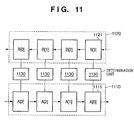
- the counterflow pipeline technique will be described below with reference to Fig. 11 .
- the counterflow pipeline technique uses first and second pipelines 1110 and 1120 as two pipelines.
- the first pipeline 1110 has a plurality of first nodes 1111, and these first nodes 1111 store data A[0] to A[3] of a first data group at a certain timing.
- the first pipeline 1110 shifts data in the right direction. As a result of the data shift, for example, the first node 1111 which stored data A[2] stores data A[3].
- the second pipeline 1120 has a plurality of nodes 1121, and these second nodes 1121 store data B[0] to B[3] of a second data group at a certain timing.
- the second pipeline 1120 shifts data in the left direction.
- Determination units 1130 are connected to the first and second nodes 1111 and 1121, and determine whether or not data stored in these nodes match.
- the two pipelines are independently shifted.
- some data may not be compared.
- data A[2] and B[1] are compared.
- data A[2] is compared with data B[3] at the next timing. Therefore, data A[2] is never compared with data B[2].
- Japanese Patent No. 3588487 the statuses of nodes of the first and second pipelines 1110 and 1120 are monitored.
- IP.COM number IPCOM000148069D in IP.COM Journal, 30 September 1979, ISSN 1533-001, XP013119002 , discloses comparison methods and hardware therefor having first and second holding means comprising a plurality of first and second nodes and shifting first and second data in opposite directions, wherein the data in each first node is compared with data in an associated second node.
- first and second holding means comprising a plurality of first and second nodes and shifting first and second data in opposite directions, wherein the data in each first node is compared with data in an associated second node.
- US 5 845 309 A discloses a cache memory system with reduced tag memory power consumption.
- the present invention provides a technique for surely and flexibly operating data using counterflow pipelines.
- the present invention in its first aspect provides an apparatus as specified in claims 1 and 3.
- the present invention in its second aspect provides a cache apparatus as specified in claim 2.
- the present invention in its third aspect provides a control method of an apparatus as specified in claim 4.
- the cache apparatus does not comprise a "cache determination unit 120" as depicted in Fig. 2 but a cache apparatus (cache determination unit) comprising a plurality of data processing apparatuses (200).
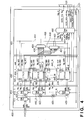
- Fig. 1 is an exemplary block diagram showing an example of the overall arrangement of an image processing apparatus 100 including a cache apparatus 110.
- a data processing apparatus (to be described later) is applied as a fully-associative cache determination unit 120.
- the image processing apparatus 100 includes a CPU 160, a DRAM 165 as an external storage device, a DRAM controller 166, and a system bus 164.
- the image processing apparatus 100 also includes an RDMAC 162 as a DMAC (Direct Memory Access Controller) used to read out data, and a WDMAC 163 used to write data, so as to read/write data from/to the DRAM 165.
- the image processing apparatus 100 further includes processing apparatuses (P.A.) A 101 to D 104 which execute processing such as image processing, and a cache apparatus 110.
- the plurality of processing apparatuses share the cache apparatus 110. That is, the cache apparatus 110 is a shared cache apparatus.
- the image processing apparatus 100 can include an arbitrary number of processing apparatuses, each of which may be configured by a pipeline circuit that executes fast permanent processing, or by a processor and programs that can flexibly change processing content although the processing speed is low.
- the CPU 160 controls the RDMAC 162, WDMAC 163, and processing apparatuses A 101 to D 104 via a control bus 161, thereby systematically controlling the overall image processing apparatus 100.
- the RDMAC 162 reads out image data stored in the DRAM 165 via the system bus 164 and DRAM controller 166, and inputs the readout image data to the processing apparatus A 101 in accordance with an instruction from the CPU 160.
- the processing apparatus A 101 executes desired image processing, and outputs image data as a processing result to the processing apparatus B 102.
- the processing apparatuses B 102, C 103, and D 104 similarly execute various kinds of image processing as in the processing apparatus A 101, and output image data as a processing result to the subsequent processing apparatuses.
- the processing apparatus D 104 outputs image data as a processing result to the WDMAC 163.
- the WDMAC 163 stores the image data received from the processing apparatus D 104 in the DRAM 165 via the system bus 164 and DRAM controller 166 in accordance with an instruction from the CPU 160.
- the image processing apparatus 100 carries out the image processing by executing the aforementioned series of operations.
- the processing apparatuses A 101 to D 104 can read out various required data (settings, a table, attribute information, etc.) from the DRAM 165 via the shared cache apparatus 110, and can use the readout data in the image processing.
- the programs may be sequentially read out via the cache apparatus 110 to implement processing.
- the aforementioned processing apparatuses A 101 to D 104 output storage addresses of data on the DRAM 165 to I/Fs 112 when they read out the data from the DRAM 165 via the cache apparatus 110.
- the cache apparatus 110 includes a ring bus 111 used for an access request, so as to transfer storage addresses of data on the DRAM 165.
- the I/Fs 112 corresponding to the respective processing apparatuses are connected to each other via this ring bus 111.
- Storage addresses 113 output from the respective processing apparatuses are input to the cache determination unit 120 via the I/Fs 112 and ring bus 111.
- the cache determination unit 120 determines a cache hit or miss based on the input storage addresses 113.
- the cache determination unit 120 includes a data processing apparatus 200 and cache determination apparatus 280.
- the storage address 113 to be input to the cache determination unit 120 (first inputs) includes:
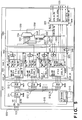
- FIG. 3 is a diagram focusing on a part of the data processing apparatus 200.
- a first pipeline 300 has a plurality of nodes (first nodes). If one of these nodes is selected as a node of interest (for example, a node 310), data elements (first data) are shifted from the node of interest to a next first node on the downstream side (for example, a node 330) in a first direction (a right direction in Fig. 1 ).
- the first pipeline 300 receives, from outside the data processing apparatus 200:
- the signals "valid", “data”, and “ID” are included in the storage address 113, and the signal “tag_id” is, for example, a default value.
- the node 310 receives:
- a data processing circuit 320 receives:
- the data processing circuit 320 applies processing to be described later to these input signals, and outputs a processing result to the node 310.
- the node 310 including a pipeline register updates data elements stored so far using data elements input from a node on the upstream side and the data processing circuit 320.
- the node 310 ignores data elements input from the upstream side, holds stored data elements intact, and does not update the data elements.
- a section including one node and a data processing circuit which inputs a processing result signal to that node will be referred to as a stage.
- a section including the node 310 and data processing circuit 320 will be referred to as a first stage.
- the node 310 outputs, to the node 330 and a data processing circuit 340 on the downstream side, stored data, that is:
- a section including the node 330 and data processing circuit 340 will be referred to as a second stage.
- various kinds of data processing are executed in the second stage.
- Data elements after the processing are temporarily stored in the node 330. This storage operation is the same as that in the first stage.
- the node 330 outputs:
- the data processing apparatus 200 includes a second pipeline 360 in addition to the first pipeline 300.
- This second pipeline 360 has a plurality of nodes (second nodes), and shifts data elements held in pipeline registers in these second nodes to neighboring nodes located in the direction (second direction) opposite to the first pipeline. More specifically, the second pipeline 360 shifts data elements from the right side on the plane of drawing as the "upstream side” to the left side on the plane of drawing as the "downstream side”. As shown in Fig. 2 , the second pipeline 360 receives an address validity signal "tag-valid" and an address signal "tag_data" from outside the data processing apparatus 200 (second inputs).
- a node 370 receives, from the upstream side, an address validity signal "tag_valid[i+2]" 372, and an address signal “tag_data[i+2]” 374. These input signals are used in the aforementioned data processing circuit 340.
- a driving signal "shift" 362 When a driving signal "shift" 362 is valid (asserted), the node 370 updates data elements stored so far using data elements input from the node on the upstream side. On the other hand, when the driving signal "shift" 362 is invalid (deasserted), the node 370 ignores data elements input from the upstream side, holds stored data elements intact, and does not update the data elements.
- a section including one node will be referred to as a stage. Especially, in Fig. 3 , a section including the node 370 will be referred to as a first stage.
- the node 370 outputs an address validity signal "tag_valid[i+1]” 382 and address signal “tag_data[i+1]” 384 stored in a pipeline register to a node 380 and the data processing circuits 320 and 340. Furthermore, the node 380 outputs a validity signal "tag_valid[i]” 392 and address signal “tag_data[i]” 394 to the downstream side. With this operation, in the second pipeline 360, the validity signal "tag_valid” and address signal “tag_data” as data elements are shifted from the right side on the plane of drawing as the "upstream side” to the left side on the plane of drawing as the "downstream side".
- the data processing circuits 320 and 340 will be described in detail below.
- the data processing circuit compares address signals “data” and "tag_data” in two directions (first comparison). When these signals are equal to each other, the data processing circuit stores a storage index ("[i]", “[i+1]”, or “[i+2]” described above) of the signal "tag_data” as a signal "tag_id". Then, the signal "tag_id” is shifted as a data processing result of the first pipeline 300 from the left side on the plane of drawing as the "upstream side” to the right side on the plane of drawing as the "downstream side” in synchronism with "data".
- the data processing circuit 320 controls a comparison circuit 324 to compare the address signal "data[l-1]" 314 and "tag_data[i+1] " 384 (second comparison).
- the selector 326 selects the input processing result signal "tag_id[l-1]" 316.
- the driving signal "shift” 362 is valid (asserted), and the second pipeline 360 operates, data elements of the second pipeline 360 are shifted to the left side on the plane of drawing as the "downstream side". Therefore, in this case, the storage index of each signal "tag_data” indicates the left neighboring storage index.
- the storage index is adjusted by decrementing the selection result of the selector 326 by "1" using a decrementer (subtractor) 328.
- the storage index selection method will be supplemented below.
- the criterion of selecting the storage index can be a simple one, for example, “preferentially selecting a storage index having a larger value”. For example, a case will be examined below wherein the data signals "data[l-1]" 314 and "tag_data[i+1]" 384 are equal to each other, and the driving signal "shift" 362 is valid.
- the input data signal "tag_id[l-1]" 316 is selected.
- the selector 346 selects the processing result signal "tag_id[l]" 336.
- the driving signal "shift” 362 is valid, and the second pipeline 360 operates accordingly, the storage index of the signal "tag_data” is shifted by "1" to the left side on the plane of drawing as the "downstream side". For this reason, the storage index is decremented by "1" using a decrementer (subtracter) 348 from the selection result of the selector 346. In this way, the match detection result can be adjusted, and more accurate and faster data processing can be implemented by simple processing.
- the data processing apparatus 200 can surely and quickly compare data elements, which are shifted in the opposing directions, in the respective stages of the pipelines.
- Each of the aforementioned data processing circuits 320 and 340 has a comparison circuit with a data element to be compared in the second pipeline 360 per data element of the first pipeline 300. Furthermore, each of the data processing circuits 320 and 340 has a new comparison circuit with an "upstream" data element of the second pipeline 360 for a data element to be compared of the second pipeline 360 under the assumption of the operation of the second pipeline 360. Since these circuits can avoid a problem of interlocking (internal stalling) for each specific stage, which may occur in the arrangement of Japanese Patent No. 3588487 , high processing performance can always be attained without stalling the data processing.
- each of the data processing circuits 320 and 340 includes the decrementer for decrementing the processing result by "1" under the assumption of the operation of the second pipeline 360. Then, the storage indices of data elements of the second pipeline are assigned in advance to increase like "0, 1, 2,..., i, i+1, i+2,..., N-1 (i and N are positive values, i ⁇ N)" from the "downstream side" toward the "upstream side” of the second pipeline. The advantage of such assignment will be described later. When the storage indices are assigned in a reverse order, the decrementer naturally serves as an incrementer used to increment the storage index by "1".
- both the first and second pipelines 300 and 360 include eight stages.
- Data Slot[0] to Data Slot[7] in Fig. 2 correspond to the nodes 310 and 330 of the first pipeline 300 shown in Fig. 3 .
- Tag Slot[0] to Tag Slot[7] in Fig. 2 correspond to the nodes 370 and 380 of the second pipeline 360 shown in Fig. 3 .
- Judge[0] to Judge[7] correspond to the data processing circuits 320 and 340 shown in Fig. 3 .
- the data processing apparatus 200 can distribute in parallel and compare many data elements by pipeline operations.
- the storage address 113 is shifted by the Data Slots of the first pipeline 300 of the data processing apparatus 200.
- the data processing apparatus 200 can simultaneously store eight signals "data_tag", and cache tag information is stored in each of these eight signals "tag_data”.
- a cache apparatus using an example of the data processing apparatus 200 corresponds to an 8-node, fully-associative cache apparatus.
- the 0th to 7th storage locations are set in series in turn from the "downstream side" of the second pipeline 360, and the second pipeline 360 has a shift structure which shifts data elements to the "downstream side" when the driving signal "shift" 362 is valid (asserted).
- an oldest cache tag is stored in the signal "tag_data” at the 0th storage location, and a newest cache tag is stored in the signal "tag_data” at the 7th storage location.
- the cache tags are shifted in turn from the signal "tag_data” at the 7th storage location to that at the 0th storage location, and are then swept out from the second pipeline 360.
- the cache determination unit 120 always discards cache tag and cache data in turn from the oldest ones although it has a very simple structure. As a result, complicated replace control of a general cache mechanism need not be executed.
- the cache hit determination sequence will be described below.
- the "cache hit determination” is to determine whether or not data designated by the storage address 113 is stored in a cache memory 190. When the designated data is stored in the cache memory 190, a cache hit is determined; otherwise, a cache miss is determined.
- the cache hit determination is made by the cache determination apparatus 280.
- the cache determination apparatus 280 determines a cache hit or miss by checking a sign bit having a 1-bit length of the processing result signal "tag_id" (2's complement representation) output from the data processing apparatus 200.
- the cache determination apparatus 280 determines a cache miss.
- the cache determination apparatus 280 determines a cache hit.
- the cache determination apparatus 280 skips determination. Also, when a signal “enable” from an access arbitration unit 130 is invalid (deasserted), the cache determination apparatus 280 skips determination.
- the address signal "data”, validity signal “valid”, and identification signal “ID” as the outputs of the data processing apparatus 200 are input to the cache determination apparatus 280 in synchronism with the signal "tag_id".
- this address signal "data” is output from the cache determination apparatus 280 as an address "cache_miss_address” at the time of a cache miss.
- the cache determination apparatus 280 validates (asserts) the driving signal "shift” 362, and outputs the address "cache_miss_address” at the time of a cache miss as the cache tag "tag_data”. Every time a cache miss is determined, the driving signal "shift” 362 is validated, and the processing result "tag_id" is decremented, as described above.
- the cache hit determination can be attained by determining the sign of the data processing result in the last stage of the first pipeline 300. Therefore, the cache determination can be done very simply.
- the cache hit determination can be attained by checking whether or not the value of the signal "tag_id" is smaller than N as the number of elements of the second pipeline.
- the cache memory 190 can use a ring type FIFO. In this case, the cache determination unit 120 and cache memory 190 can be easily synchronized. Note that when the cache determination indicates a cache hit, desired cache data is stored in the cache memory at a position indicated by "tag_id".
- the cache determination unit 120 outputs, to the access arbitration unit 130, as a determination result 125 based on the input storage address 113:
- the operation of the access arbitration unit 130 will be described below with reference to Fig. 1 .
- the validity signal "valid" in the determination result 125 is valid (asserted)
- the access arbitration unit 130 operates; otherwise, it waits.
- the access arbitration unit 130 executes the following processing according to a valid (asserted)/invalid (deasserted) status of the cache determination result "cache_miss_flag" in the determination result 125.
- the cache memory arbitration unit 180 evaluates whether or not data are held in the storage areas of the receiving queue 170 and waiting queue 140.
- the cache memory arbitration unit 180 dequeues the cache determination result "ID, tag_id, cache_miss_flag" to be processed from the waiting queue 140.
- the cache memory arbitration unit 180 waits without any processing.
- the cache memory arbitration unit 180 executes the following processing depending on whether the cache determination result "cache_miss_flag" is invalid (deasserted) or valid (asserted).
- the cache apparatus 110 distributes cache data obtained by the aforementioned process to the processing apparatuses 101 to 104.
- the cache apparatus 110 includes a ring bus 115 used to distribute cache data.
- the I/Fs 116 corresponding to these processing apparatuses are connected to each other via this ring bus 115.
- Each of the I/Fs 116 connected to the respective processing apparatuses receives the cache data "valid, ID, cache_data" 185 as the output from the cache memory arbitration unit 180. Then, when the identification signal "ID" of the received cache data matches that of the connected processing apparatus, the corresponding I/F 116 outputs the cache data to the processing apparatus. If the two identification signals do not match, each I/F 116 sends the received cache data to another I/F 116 located at the subsequent position via the ring bus 115.
- the cache apparatus 110 adopts a non-blocking cache mechanism so as to hide refill latency as a penalty at the time of a cache miss.
- This mechanism saves information "ID, tag_id, cache_miss_flag" 135, which is required later, in the waiting queue 140 even when the determination result 125 indicates a cache miss.
- the cache apparatus 110 executes cache determination processing of the next pixel before completion of processing for reading out cache-missed data from the DRAM 165, and storing it in the cache memory 190. With this processing, the cache apparatus 110 can execute the cache determination for the subsequent pixel even while the cache-missed data is refilled from the DRAM 165 to the cache memory 190. Therefore, a performance degradation at the time of a cache miss can be suppressed.
- the cache apparatus 110 can implement a fully-associative cache apparatus, which can be shared by a plurality of processing apparatuses, using a very simple mechanism.
- addresses having low correlations are successively input to the cache determination unit 120.
- a cache determination unit which adopts a general direct mapping method calculates a storage address of a tag memory used to manage a cache tag from lower bits of each address, a cache conflict is readily caused by such addresses having low correlations.
- To increase the number of set-associative nodes in correspondence with the number of processing apparatuses is one solution to reduce the cache conflict probability. However, when the number of processing apparatuses becomes very large, a very large number of nodes have to be coped with.
- the cache determination unit 120 attains determination by the pipeline configuration, it can operate at a very high operation frequency.
- the cache determination unit 120 does not require any complicated replace control at the time of a cache conflict, which is required in the related art, since data are automatically deleted in turn from older data. For this reason, the cache determination unit 120 and cache memory arbitration unit 180 can be synchronized by a very simple mechanism, and a FIFO can be used as the cache memory.
- such arrangement is advantageous to improve the operation frequency of the cache apparatus 110. More importantly, the cache apparatus 110 adopts the fully-associative method, and never causes a cache conflict due to the same lower bits of addresses.
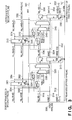
- FIG. 4 is a circuit diagram for explaining an example of the circuit arrangement of the cache determination unit 400.
- the cache determination unit 400 could be used in place of the cache determination unit 120 of the cache apparatus 110 shown in Fig. 1 .
- a description of the same parts as in the basic arrangement of the aforementioned cache apparatus 110 will not be repeated.
- the cache determination unit 400 includes a replicating apparatus 410, operation apparatus 430, and cache determination apparatus 480.
- the operation apparatus 430 includes a plurality of data processing apparatuses (D.P.A.) 200_1 to 200_N, each of which has the same arrangement as that of the data processing apparatus 200 described using Fig. 2 .
- the cache determination unit 400 includes the plurality of data processing apparatuses described above, the number of data elements which can be compared at the same time is increased. Since the cache determination unit 400 shown in Fig. 4 includes the plurality of basic data processing apparatuses, a data processing apparatus which has already been designed and verified can be re-used, thus improving the development efficiency.
- Respective Data Slots included in the cache determination unit 400 are the same as the nodes 310 and 330 shown in Fig. 3 , and updates a data element stored so far using a new data element when the signal "enable” 121 is valid (asserted).
- a node 411 receives the storage address 113 from the I/F 112. As described above, the storage address 113 includes the validity signal "valid", address signal "data”, and identification signal "ID”.
- the replicating apparatus 410 replicates the storage address 113 to retime it in nodes 412 1 to 412_N as indicated by 420.
- the nodes 412_1 to 412_N respectively output stored data elements to the first pipelines 300 of the corresponding data processing apparatuses 200_1 to 200_N. In this way, replicas of the same storage address 113 are input in parallel to the first pipelines 300 of the respective data processing apparatuses at the same timing.
- the operation apparatus 430 receives a signal "cache_miss_flag” 444 output from a decoder 452 of the cache determination apparatus 480 as the driving signal "shift", which is input to the respective data processing apparatuses 200_1 to 200_N. Then, data elements of the second pipelines 360 of all the data processing apparatuses 200_1 to 200_N are synchronously shifted. Signals "cache_miss_flag” and “cache_miss_address" output from the cache determination apparatus 480 are input to the second pipeline 360 of the data processing apparatus (1) 200_1 as signals "tag_valid" and "tag_data”.
- Signals “tag_valid” and “tag_data” output from the second pipeline 360 of the data processing apparatus (1) are input to the second pipeline 360 of the data processing apparatus (2) 200_2 as signals “tag_valid” and “tag_data” (440_1).
- Signals “tag_valid” and “tag_data” output from the second pipeline 360 of the data processing apparatus (i) are input to the second pipeline 360 of the data processing apparatus (i+1) as signals “tag_valid” and "tag_data”.
- the data processing apparatuses are sequentially connected so that the outputs "tag_valid, tag_data" of the second pipeline of a certain data processing apparatus are connected in series to the inputs of the second pipeline of the subsequent data processing apparatus.
- the cache determination apparatus 480 receives processing results "tag_id(1), tag_id(2),..., tag_id(N)" 450 from all the data processing apparatuses 200_1 to 200_N.
- the cache determination apparatus 480 further receives signals "valid, data” output from the first pipeline 300 of any one of the data processing apparatuses 200_1 to 200_N.
- the decoder 452 confirms if a validity signal “valid” 453 is valid (asserted) and the signal "enable” 121 is valid. If both the signals are valid, the cache determination apparatus 480 controls the decoder 452 to confirm sign bits 451 of the N processing results "tag_id(1), tag_id(2),..., tag_id(N)" 450.
- the decoder 452 determines a cache hit as a cache determination result, and outputs "0" as the signal "cache_miss_flag” 444. If all the sign bits 451 are "1”, the decoder 452 determines a cache miss as a cache determination result, and outputs "1" as the signal "cache_miss_flag” 444. In case of a cache hit, the decoder 452 outputs a number 456 of the data processing apparatus corresponding to "0" of the sign bits to a selector 454.
- the selector 454 selects "tag_id” of the data processing apparatus indicated by the number 456 from the processing results "tag_id(1), tag_id(2),..., tag_id(N)" 450, and outputs it as a signal "tag_id” 458.
- a node 460 updates data elements stored so far using the input data elements. Then, the node 460 outputs data elements stored by itself to the access arbitration unit 130 as the determination result 125.
- the cache apparatus using the cache determination unit 400 includes a plurality of data processing apparatuses each having the basic arrangement, and can be implemented by connecting only the first pipelines 300 and second pipelines 360 of the respective data processing apparatuses. For this reason, a data processing apparatus which has already been designed and verified can be re-used.
- the cache determination unit 400 executes data processing using the pipeline configuration, and can determine a cache miss by calculating only logical products of all sign bits. In this manner, the cache apparatus can operate at a very higher operation frequency than the conventional cache apparatus.
- data elements "tag_data, tag_valid” may be swept out as the outputs of the second pipeline 360 of the data processing apparatus (N) 200_N located at the rearmost position. These swept-out data elements are output to the node 460, which may output the determination result 125 including these data elements as "sweep_address, sweep_address_valid" to the access arbitration unit 130. Using these data elements, a write-back cache apparatus can be implemented.
- the storage address 113 to be output includes:
- the write data "write_data” is written at a storage address of the cache memory 190.
- the write flag "write_enable” is invalid (deasserted)
- the operation of the aforementioned read cache apparatus is performed.
- the data elements "write_enable” and “write_data” are shifted in the first pipelines 300 of the respective data processing apparatuses 200_1 to 200_N in the cache determination unit 400 in synchronism with other data elements included in the storage address 113.
- the data processing apparatus (N) 200_N outputs the data elements "write_enable” and “write_data” to the node 460 in synchronism with other data elements.
- the node 460 outputs the determination result 125 including these data to the access arbitration unit 130. That is, this determination result 125 includes:
- the determination result 125 arrives the cache memory arbitration unit 180 via the waiting queue 140.
- the cache memory arbitration unit 180 calculates a storage address of the cache memory 190 using "ID, tag_id" in the same manner as described above.
- the cache memory arbitration unit 180 writes the write data "write_data” at the storage address of the cache memory 190.
- the cache memory arbitration unit 180 cannot immediately write the write data "write_data” in the cache memory 190.
- the cache memory arbitration unit 180 When the swept-out address validity signal "sweep_address_valid" is valid (asserted), data temporarily stored at the storage address of the cache memory 190 is overwritten. Hence, the cache memory arbitration unit 180 reads out cache data at the storage address from the cache memory 190, and saves this cache data in an area of the DRAM 165 indicated by the swept-out address signal "sweep_address". After that, the cache memory arbitration unit 180 refills data in an area of the DRAM 165 as an external memory indicated by the address signal "cache_miss_address" in the cache memory 190.
- the cache memory arbitration unit 180 overwrites the data read out from the DRAM 165 by the write data "write_data", and temporarily stores the overwritten data at the storage address of the cache memory 190.
- the cache memory arbitration unit 180 may skip this refill operation.
- the swept-out address signal "sweep_address_valid” is invalid (deasserted)
- valid cache data is not temporarily stored at the storage address of the cache memory 190. Therefore, the cache memory arbitration unit 180 need not save cache data temporarily stored at the storage address of the cache memory 190. In this case, the cache memory arbitration unit 180 may temporarily store the data "write_data" as cache data at the storage address of the cache memory 190 while performing the aforementioned refill operation if necessary.
- the write-back cache apparatus can be easily implemented.
- the cache determination unit 400 of the cache apparatus used as the write-back cache apparatus also has the same advantages as those of the read cache apparatus. Especially, data are automatically deleted in turn from older data, and complicated replace control at the time of a cache conflict need not be executed. Then, cache data temporarily stored in the cache memory need only be saved in turn from older data in the DRAM 165 as an external memory. As described above, write-back control unique to the write-back cache apparatus can be implemented by a very simple method.
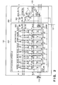
- FIG. 5 is an exemplary circuit diagram for explaining the circuit arrangement of the cache determination unit 500 according to an embodiment of the present invention, including a partition information table.
- the cache determination unit 500 is used in place of the cache determination unit 120 of the cache apparatus 110 shown in Fig. 1 .
- the cache determination unit 500 includes a replicating apparatus 510, operation apparatus 530, and cache determination apparatus 580.
- the operation apparatus 530 includes a plurality of data processing apparatuses 200_1 to 200_N, each of which has the same arrangement as that of the data processing apparatus 200 described using Fig. 2 .
- the cache determination unit 500 includes the plurality of data processing apparatuses described above, thereby increasing the number of data elements which can be compared at the same time.
- the cache determination unit 500 can switch a cache capacity (the number of nodes) to be exclusively used by each processing apparatus for respective processing apparatuses.
- a larger cache capacity (the number of nodes) can be assigned to image processing with a high priority level. That is, upon execution of image processing, the exclusive assignment of a cache capacity (the number of nodes) is adaptively switched according to the purpose of image processing, thus executing the image processing with a desired efficiency.
- the replicating apparatus 510 shown in Fig. 5 includes a partition information table 515 unlike in the replicating apparatus 410. Therefore, a description of parts common to those in the replicating apparatus 410 will not be given, and the partition information table 515 will be described below.
- the partition information table 515 the CPU 160 sets partition information in advance so as to switch assignments of cache capacities (the numbers of nodes) to be exclusively used by respective processing apparatuses.
- the partition information represents assignments (groups) of the data processing apparatuses 200_1 to 200_N to be exclusively used by the respective processing apparatuses.
- the partition information table 515 will be described in detail below with reference to Figs. 7 and 8 .
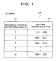
- the partition information table 515 allows to set partition information 704 for each identification signal ID 702 of the processing apparatus, as in a format 700 shown in Fig. 7 .
- the N-bit partition information 704 serves as a flag, each bit of which indicates whether or not the data processing apparatus 200 indicated by that bit is to be used, in turn from the most significant bit. When each bit is "1", it indicates ⁇ use> of the indicated data processing apparatus; when it is "0", it indicates ⁇ nonuse>.
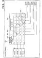
- FIG. 8 A practical example 800 of the partition information table 515 will be described below with reference to Fig. 8 .
- the partition information of the processing apparatus A 101 is "10000000", and has a setting indicating that the processing apparatus A 101 uses the data processing apparatus (1) (shown at 820) but it does not use the remaining data processing apparatuses (2) to (8).
- the partition information of the processing apparatus B 102 is "01110000”, and has a setting indicating that the processing apparatus B 102 uses the data processing apparatuses (2) to (4) (shown at 822), but it does not use the remaining data processing apparatuses (1) and (5) to (8).
- a setting of the processing apparatus C 103 indicates that it uses the data processing apparatuses (5) and (7), but it does not use the remaining data processing apparatuses.
- a setting of the processing apparatus D 104 indicates that it uses the data processing apparatuses (6) and (8), but it does not use the remaining data processing apparatuses.
- the processing apparatus A 101 exclusively uses the data processing apparatus (1)
- the processing apparatus B 102 exclusively uses the data processing apparatuses (2) to (4)
- the processing apparatus C 103 exclusively uses the data processing apparatuses (5) and (7)
- the processing apparatus D 104 exclusively uses the data processing apparatuses (6) and (8).
- the settings of the pieces of partition information 704 need only be exclusive among the plurality of processing apparatuses, and the data processing apparatuses may be discontinuously assigned like in the settings of the processing apparatuses C 103 and D 104 (shown at 824).
- the replicating apparatus 510 reads out, using an input identification signal "ID”, partition information "partition” 518 corresponding to this identification signal "ID” from the partition information table 515, and inputs the readout information to a node 511.
- the node 511 replicates an input validity signal “valid” and input data signals “data, ID, partition”, and outputs them to nodes 512_1 to 512_N.
- the nodes 512_1 to 512_N respectively output data elements stored by themselves to the first pipelines 300 of the corresponding data processing apparatuses 200_1 to 200_N. In this manner, the replicating apparatus 510 replicates data elements as many as the number of data processing apparatuses 200 to retime them.
- the second pipelines 360 of the respective data processing apparatuses are connected, as indicated by a broken line part 540.
- the connections of the second pipelines 360 are automatically switched according to partition information "partition" 535 output from the data processing apparatus (N) 200_N.
- the operation apparatus 530 respectively calculates logical products of a signal "cache_miss_flag” 559 output from a decoder 552 and respective bits corresponding to the data processing apparatuses (1) to (N) of the partition information "partition” 535 output from the data processing apparatus (N).
- the operation apparatus 530 inputs the calculated logical products as driving signals "shift" of the corresponding data processing apparatuses (544_1, 544_2,..., 544_N).
- data elements of the second pipelines 360 of only the data processing apparatuses corresponding to ⁇ use> in the partition information of all the data processing apparatuses are synchronously shifted.
- the operation apparatus 530 compiles data elements required to switch the connections of the second pipelines 360.
- Data elements 532_1 to 532_N, "cache_miss_flag” 559, and "cache_miss_address(data)" 555 output from the second pipelines 360 of the respective data processing apparatuses (1) to (N) are bundled on a bus 542.
- data are input from the bus 542 to selectors 545_1, 545_2,..., 545_N used to select inputs to the second pipelines 360 of the data processing apparatuses (1) to (N).
- the selectors 545_1, 545_2,..., 545_N select corresponding data elements based on the partition information "partition” 535, and inputs the selected data elements to the second pipelines 360 of the data processing apparatuses (1) to (N). Also, a selector 548 used to output data elements which are swept out at the time of a cache miss may be added. Swept-out data elements are selected from the bus 542 based on the partition information "partition” 535, and are output as data elements "sweep_address, sweep_address_valid". As described above, these data elements are used when the cache apparatus 110 is used as the write-back cache apparatus.
- the input selection method to the second pipelines in the practical example 800 is as follows.
- an identification number "ID" output from the first pipeline 300 of the data processing apparatus (N) is "1”
- the partition information includes the setting "10000000”, as can be seen from the practical example 800.
- the second pipeline 360 of the data processing apparatus (1) is shifted.
- data "cache_miss_flag” 559 and "cache_miss_address(data)" 555 are selected from those on the bus 542.
- data "cache_miss_flag” 559 and “cache_miss_address(data)" 555 are selected from those on the bus 542.
- the outputs 532_2 from the second pipeline of the data processing apparatus (2) are selected.
- the outputs from the second pipeline of the data processing apparatus (3) are selected.
- swept-out data elements "sweep_address, sweep_address_valid” the outputs from the second pipeline of the data processing apparatus (4) are selected.
- the second pipelines are connected in turn in ascending order of apparatus number of the data processing apparatuses. That is, the outputs from the second pipeline of the data processing apparatus to be used need only be connected in series with the inputs of the second pipeline of the next data processing apparatus to be used according to the setting of the partition information "partition" 535.
- the cache determination apparatus 580 receives processing results "tag_id(1), tag_id(2),..., tag_id(N)" 550 of all the data processing apparatuses 200_1 to 200_N.
- the cache determination apparatus 580 receives signals "valid, data, ID, partition” from any one of the data processing apparatuses 200_1 to 200_N. In Fig. 5 , these signals are input from the data processing apparatus (N) 200_N, but they may be input from another data processing apparatus.
- the decoder 552 receives the partition information "partition" 535 unlike the decoder 452. The decoder 552 will be described in detail below with reference to Fig. 6 .
- the decoder 552 calculates logical products of the following four signals (1-bit signals):
- the cache determination apparatus 580 selects a processing result "tag_id” 558 at the time of a cache hit from the plurality of processing results "tag_id(1) to tag_id(N)" 550 based on the cache hit apparatus number 556 using the selector 554, and outputs it to a node 560.
- the operation of the cache memory arbitration unit 180 of the cache apparatus using the cache determination unit 500 and the arrangement of a cache memory 900 will be described below.
- the cache memory 900 shown in Fig. 9 will be described first.
- the cache memory 900 is used in place of the cache memory 190 shown in Fig. 1 .
- the cache memory 900 is also configured by a FIFO.
- the cache memory 900 is divided into areas corresponding to the data processing apparatuses (1) to (N). According to the setting of the partition information, a base pointer as a reference of the FIFO and the number of lines of each area are determined for each ID. Even when areas are discontinuous like in the part 824 of the practical example 800, areas to be used are continuously assured by the function of the aforementioned second pipeline connection switching device.
- the cache memory arbitration unit 180 acquires the aforementioned base pointer and the number of lines according to the readout "ID” and a write pointer for each ID. When a cache hit is determined, the cache memory arbitration unit 180 calculates an address based on the result "tag_id", which is read out at the same time, and the base pointer and write pointer of the cache memory 900. Then, the cache memory arbitration unit 180 writes readout cache data in a storage area indicated by the total value of the base pointer and write pointer of the cache memory 900 as data "write_data" 182.
- the cache determination unit 500 executes data processing using the pipeline configuration. By calculating at most 1-bit logical products of inverted sign bits of outputs corresponding to the respective data processing apparatuses and partition information, a cache hit can be determined. As a result, the cache apparatus can operate at a very high operation frequency compared to the conventional cache apparatus. Since data are automatically deleted in turn from older data, complicated replace control at the time of a cache conflict is not required. Also, the cache memory requires only ring type FIFO operations for predetermined areas. In order to implement the cache memory 900, a multi-bank FIFO having a plurality of write pointers need only be used. Also, the cache memory 900 can be implemented using a plurality of FIFOs. In the example of the above description, the partition information table is prepared, and the partition information is switched for each processing apparatus. However, the above processing can be implemented when each processing apparatus designates partition information for respective processing contents (operation statuses) of the processing apparatus.
- the respective nodes of the first pipelines 300 and second pipelines 360 of the plurality of data processing apparatuses (1) to (N) described in Fig. 5 operate based on clock signals of one system (not shown). However, the plurality of data processing apparatuses (1) to (N) may be operated by respectively inputting in-phase clocks signals of different systems to the data processing apparatuses (1) to (N). Upon prioritizing power savings, clock signals to one of the data processing apparatuses (1) to (N) are stopped to stop that data processing apparatus.
- the cache memory 900 is implemented using different SRAMs for respective areas of the data processing apparatuses (1) to (N). In correspondence with the stopped data processing apparatuses, supplies of clock signals (or power supply voltages) to the SRAMs which are not used are stopped. In this way, further power savings can be attained.
- Fig. 10 is an exemplary circuit diagram for explaining the arrangement in which crossbar switches are used in place of the ring buses.
- Fig. 10 shows an example of connections between M processing apparatuses (1) to (M) and N data processing apparatuses (1) to (N), which connections are attained via crossbar switches 1020 and 1060 in place of the aforementioned connections via the ring buses.
- the crossbar switches 1020 and 1060 which are switched based on partition information "partition" are inserted before and after the data processing apparatuses.
- the plurality of processing apparatuses can use the plurality of data processing apparatuses in parallel. With such parallel processes, the plurality of processing apparatuses can be speeded up.
- aspects of the present invention can also be realized by a computer of a system or apparatus (or devices such as a CPU or MPU) that reads out and executes a program recorded on a memory device to perform the functions of the above-described embodiment(s), and by a method, the steps of which are performed by a computer of a system or apparatus by, for example, reading out and executing a program recorded on a memory device to perform the functions of the above-described embodiment(s).
- the program is provided to the computer for example via a network or from a recording medium of various types serving as the memory device (for example, computer-readable medium).
Landscapes
- Engineering & Computer Science (AREA)
- Theoretical Computer Science (AREA)
- Physics & Mathematics (AREA)
- General Physics & Mathematics (AREA)
- General Engineering & Computer Science (AREA)
- Computational Mathematics (AREA)
- Mathematical Analysis (AREA)
- Mathematical Optimization (AREA)
- Pure & Applied Mathematics (AREA)
- Memory System Of A Hierarchy Structure (AREA)
- Advance Control (AREA)
Applications Claiming Priority (2)
| Application Number | Priority Date | Filing Date | Title |
|---|---|---|---|
| JP2010130447A JP5650441B2 (ja) | 2010-06-07 | 2010-06-07 | 演算装置、キャッシュ装置、その制御方法及びコンピュータプログラム |
| EP11164892.9A EP2393004B1 (en) | 2010-06-07 | 2011-05-05 | Cache apparatus and control method thereof |
Related Parent Applications (3)
| Application Number | Title | Priority Date | Filing Date |
|---|---|---|---|
| EP11164892.9A Division-Into EP2393004B1 (en) | 2010-06-07 | 2011-05-05 | Cache apparatus and control method thereof |
| EP11164892.9A Division EP2393004B1 (en) | 2010-06-07 | 2011-05-05 | Cache apparatus and control method thereof |
| EP11164892.9 Division | 2011-05-05 |
Publications (2)
| Publication Number | Publication Date |
|---|---|
| EP2437159A1 EP2437159A1 (en) | 2012-04-04 |
| EP2437159B1 true EP2437159B1 (en) | 2018-10-31 |
Family
ID=44352182
Family Applications (2)
| Application Number | Title | Priority Date | Filing Date |
|---|---|---|---|
| EP11195127.3A Active EP2437159B1 (en) | 2010-06-07 | 2011-05-05 | Apparatus for data comparison and control method thereof |
| EP11164892.9A Not-in-force EP2393004B1 (en) | 2010-06-07 | 2011-05-05 | Cache apparatus and control method thereof |
Family Applications After (1)
| Application Number | Title | Priority Date | Filing Date |
|---|---|---|---|
| EP11164892.9A Not-in-force EP2393004B1 (en) | 2010-06-07 | 2011-05-05 | Cache apparatus and control method thereof |
Country Status (4)
| Country | Link |
|---|---|
| US (1) | US8812783B2 (enExample) |
| EP (2) | EP2437159B1 (enExample) |
| JP (1) | JP5650441B2 (enExample) |
| CN (1) | CN102331922B (enExample) |
Families Citing this family (6)
| Publication number | Priority date | Publication date | Assignee | Title |
|---|---|---|---|---|
| US8862702B2 (en) * | 2012-07-18 | 2014-10-14 | Accedian Networks Inc. | Systems and methods of installing and operating devices without explicit network addresses |
| JP2015013429A (ja) * | 2013-07-05 | 2015-01-22 | キヤノン株式会社 | 画像処理装置及びその制御方法、並びにプログラム |
| CN107016008B (zh) * | 2016-06-06 | 2020-06-09 | 阿里巴巴集团控股有限公司 | 信息处理方法和装置及动态信息的显示方法和装置 |
| JP7278067B2 (ja) | 2018-12-20 | 2023-05-19 | キヤノン株式会社 | データ処理装置及びその制御方法及びプログラム |
| US11442868B2 (en) | 2019-05-24 | 2022-09-13 | Texas Instruments Incorporated | Aggressive write flush scheme for a victim cache |
| CN113672286B (zh) * | 2021-07-30 | 2024-10-01 | 奇点微(上海)光电科技有限公司 | 一种流水线求值器、移动轨迹分析处理装置、方法及设备 |
Citations (1)
| Publication number | Priority date | Publication date | Assignee | Title |
|---|---|---|---|---|
| US5845309A (en) * | 1995-03-27 | 1998-12-01 | Kabushiki Kaisha Toshiba | Cache memory system with reduced tag memory power consumption |
Family Cites Families (26)
| Publication number | Priority date | Publication date | Assignee | Title |
|---|---|---|---|---|
| US5163142A (en) * | 1988-10-28 | 1992-11-10 | Hewlett-Packard Company | Efficient cache write technique through deferred tag modification |
| JPH04178755A (ja) * | 1990-11-13 | 1992-06-25 | Toshiba Corp | データ統合装置 |
| US5353424A (en) * | 1991-11-19 | 1994-10-04 | Digital Equipment Corporation | Fast tag compare and bank select in set associative cache |
| US5386527A (en) * | 1991-12-27 | 1995-01-31 | Texas Instruments Incorporated | Method and system for high-speed virtual-to-physical address translation and cache tag matching |
| JPH05324468A (ja) * | 1992-05-21 | 1993-12-07 | Fujitsu Ltd | 階層化キャッシュメモリ |
| DE69430352T2 (de) * | 1993-10-21 | 2003-01-30 | Sun Microsystems Inc., Mountain View | Gegenflusspipeline |
| US5710905A (en) * | 1995-12-21 | 1998-01-20 | Cypress Semiconductor Corp. | Cache controller for a non-symetric cache system |
| US5905680A (en) * | 1996-04-30 | 1999-05-18 | Texas Instruments Incorporated | Self-timed comparison circuits and systems |
| JPH10190744A (ja) * | 1996-12-26 | 1998-07-21 | Toshiba Corp | 情報記憶装置 |
| US5748539A (en) * | 1997-03-05 | 1998-05-05 | Sun Microsystems, Inc. | Recursive multi-channel interface |
| JP3623082B2 (ja) * | 1997-09-26 | 2005-02-23 | 日本電信電話株式会社 | 連想メモリモジュール |
| US6825848B1 (en) * | 1999-09-17 | 2004-11-30 | S3 Graphics Co., Ltd. | Synchronized two-level graphics processing cache |
| US6862670B2 (en) | 2001-10-23 | 2005-03-01 | Ip-First, Llc | Tagged address stack and microprocessor using same |
| US6754772B2 (en) * | 2001-11-15 | 2004-06-22 | Micron Technology, Inc. | Distributed cache |
| US7502887B2 (en) * | 2003-11-12 | 2009-03-10 | Panasonic Corporation | N-way set associative cache memory and control method thereof |
| US7689772B2 (en) * | 2006-05-04 | 2010-03-30 | Intel Corporation | Power-performance modulation in caches using a smart least recently used scheme |
| US7546405B2 (en) * | 2006-09-26 | 2009-06-09 | Sony Computer Entertainment Inc. | Methods and apparatus for dynamic grouping of requestors of resources in a multi-processor system |
| US7991960B2 (en) * | 2006-10-11 | 2011-08-02 | Arm Limited | Adaptive comparison control in a data store |
| KR101077513B1 (ko) * | 2007-06-20 | 2011-10-28 | 후지쯔 가부시끼가이샤 | 캐시 메모리 장치, 연산 처리 장치 및 그 제어 방법 |
| US7913007B2 (en) * | 2007-09-27 | 2011-03-22 | The University Of North Carolina | Systems, methods, and computer readable media for preemption in asynchronous systems using anti-tokens |
| JP2010102623A (ja) * | 2008-10-27 | 2010-05-06 | Nec Electronics Corp | キャッシュメモリ及びその制御方法 |
| US8539185B2 (en) * | 2008-11-13 | 2013-09-17 | International Business Machines Corporation | Systolic networks for a spiral cache |
| US8271728B2 (en) * | 2008-11-13 | 2012-09-18 | International Business Machines Corporation | Spiral cache power management, adaptive sizing and interface operations |
| US8051337B2 (en) * | 2009-01-22 | 2011-11-01 | Taiwan Semiconductor Manufacturing Company, Ltd. | System and method for fast cache-hit detection |
| US8452944B2 (en) * | 2009-05-22 | 2013-05-28 | Canon Kabushiki Kaisha | Information processing apparatus and information processing method |
| JP5627330B2 (ja) * | 2010-08-02 | 2014-11-19 | キヤノン株式会社 | 情報処理装置、キャッシュ装置およびデータ処理方法 |
-
2010
- 2010-06-07 JP JP2010130447A patent/JP5650441B2/ja active Active
-
2011
- 2011-05-05 EP EP11195127.3A patent/EP2437159B1/en active Active
- 2011-05-05 EP EP11164892.9A patent/EP2393004B1/en not_active Not-in-force
- 2011-05-11 US US13/105,062 patent/US8812783B2/en active Active
- 2011-06-01 CN CN201110145879.5A patent/CN102331922B/zh not_active Expired - Fee Related
Patent Citations (1)
| Publication number | Priority date | Publication date | Assignee | Title |
|---|---|---|---|---|
| US5845309A (en) * | 1995-03-27 | 1998-12-01 | Kabushiki Kaisha Toshiba | Cache memory system with reduced tag memory power consumption |
Also Published As
| Publication number | Publication date |
|---|---|
| US8812783B2 (en) | 2014-08-19 |
| CN102331922A (zh) | 2012-01-25 |
| EP2437159A1 (en) | 2012-04-04 |
| US20110302373A1 (en) | 2011-12-08 |
| EP2393004A1 (en) | 2011-12-07 |
| JP5650441B2 (ja) | 2015-01-07 |
| EP2393004B1 (en) | 2018-10-31 |
| JP2011257880A (ja) | 2011-12-22 |
| CN102331922B (zh) | 2015-07-15 |
Similar Documents
| Publication | Publication Date | Title |
|---|---|---|
| US6625654B1 (en) | Thread signaling in multi-threaded network processor | |
| EP2437159B1 (en) | Apparatus for data comparison and control method thereof | |
| US7925804B2 (en) | FIFO device and method of storing data in FIFO buffer | |
| JP5895840B2 (ja) | マルチプロセッサシステム、実行制御方法、実行制御プログラム | |
| WO1994027216A1 (en) | Multiprocessor coupling system with integrated compile and run time scheduling for parallelism | |
| US20230063751A1 (en) | A processor system and method for increasing data-transfer bandwidth during execution of a scheduled parallel process | |
| US8190794B2 (en) | Control function for memory based buffers | |
| US8819360B2 (en) | Information processing apparatus, cache apparatus, and data processing method | |
| US7054969B1 (en) | Apparatus for use in a computer system | |
| US10152329B2 (en) | Pre-scheduled replays of divergent operations | |
| US5668975A (en) | Method of requesting data by interlacing critical and non-critical data words of multiple data requests and apparatus therefor | |
| US7155540B2 (en) | Data communication method in shared memory multiprocessor system | |
| CN113791892B (zh) | 数据通路仲裁方法、数据通路仲裁装置及芯片 | |
| CN118467418B (zh) | 一种存储访问系统以及存储访问调度方法 | |
| EP1512079A2 (en) | Pseudo multiport data memory has stall facility | |
| US20030182517A1 (en) | Method and system for buffering multiple requests from multiple devices to a memory | |
| US6654861B2 (en) | Method to manage multiple communication queues in an 8-bit microcontroller | |
| CN100422978C (zh) | 具有多个互相通信的数字信号处理器的集成电路 | |
| CN119065861B (zh) | 一种访问请求处理方法和电子设备 | |
| JPH10124438A (ja) | 入出力処理装置 | |
| JP2012173847A (ja) | バス調停装置およびバス調停方法 | |
| GB2341766A (en) | Bus architecture | |
| GB2341765A (en) | Bus idle usage | |
| GB2341768A (en) | Bus arbitration | |
| GB2341770A (en) | Modular bus topology |
Legal Events
| Date | Code | Title | Description |
|---|---|---|---|
| PUAI | Public reference made under article 153(3) epc to a published international application that has entered the european phase |
Free format text: ORIGINAL CODE: 0009012 |
|
| AC | Divisional application: reference to earlier application |
Ref document number: 2393004 Country of ref document: EP Kind code of ref document: P |
|
| AK | Designated contracting states |
Kind code of ref document: A1 Designated state(s): AL AT BE BG CH CY CZ DE DK EE ES FI FR GB GR HR HU IE IS IT LI LT LU LV MC MK MT NL NO PL PT RO RS SE SI SK SM TR |
|
| AX | Request for extension of the european patent |
Extension state: BA ME |
|
| 17P | Request for examination filed |
Effective date: 20121004 |
|
| 17Q | First examination report despatched |
Effective date: 20160727 |
|
| STAA | Information on the status of an ep patent application or granted ep patent |
Free format text: STATUS: EXAMINATION IS IN PROGRESS |
|
| GRAP | Despatch of communication of intention to grant a patent |
Free format text: ORIGINAL CODE: EPIDOSNIGR1 |
|
| STAA | Information on the status of an ep patent application or granted ep patent |
Free format text: STATUS: GRANT OF PATENT IS INTENDED |
|
| INTG | Intention to grant announced |
Effective date: 20180503 |
|
| GRAJ | Information related to disapproval of communication of intention to grant by the applicant or resumption of examination proceedings by the epo deleted |
Free format text: ORIGINAL CODE: EPIDOSDIGR1 |
|
| STAA | Information on the status of an ep patent application or granted ep patent |
Free format text: STATUS: EXAMINATION IS IN PROGRESS |
|
| GRAR | Information related to intention to grant a patent recorded |
Free format text: ORIGINAL CODE: EPIDOSNIGR71 |
|
| GRAS | Grant fee paid |
Free format text: ORIGINAL CODE: EPIDOSNIGR3 |
|
| STAA | Information on the status of an ep patent application or granted ep patent |
Free format text: STATUS: GRANT OF PATENT IS INTENDED |
|
| GRAA | (expected) grant |
Free format text: ORIGINAL CODE: 0009210 |
|
| STAA | Information on the status of an ep patent application or granted ep patent |
Free format text: STATUS: THE PATENT HAS BEEN GRANTED |
|
| INTC | Intention to grant announced (deleted) | ||
| AC | Divisional application: reference to earlier application |
Ref document number: 2393004 Country of ref document: EP Kind code of ref document: P |
|
| AK | Designated contracting states |
Kind code of ref document: B1 Designated state(s): AL AT BE BG CH CY CZ DE DK EE ES FI FR GB GR HR HU IE IS IT LI LT LU LV MC MK MT NL NO PL PT RO RS SE SI SK SM TR |
|
| INTG | Intention to grant announced |
Effective date: 20180924 |
|
| REG | Reference to a national code |
Ref country code: CH Ref legal event code: EP Ref country code: GB Ref legal event code: FG4D |
|
| REG | Reference to a national code |
Ref country code: AT Ref legal event code: REF Ref document number: 1060211 Country of ref document: AT Kind code of ref document: T Effective date: 20181115 |
|
| REG | Reference to a national code |
Ref country code: IE Ref legal event code: FG4D |
|
| REG | Reference to a national code |
Ref country code: DE Ref legal event code: R096 Ref document number: 602011053381 Country of ref document: DE |
|
| REG | Reference to a national code |
Ref country code: NL Ref legal event code: MP Effective date: 20181031 |
|
| REG | Reference to a national code |
Ref country code: LT Ref legal event code: MG4D |
|
| REG | Reference to a national code |
Ref country code: AT Ref legal event code: MK05 Ref document number: 1060211 Country of ref document: AT Kind code of ref document: T Effective date: 20181031 |
|
| PG25 | Lapsed in a contracting state [announced via postgrant information from national office to epo] |
Ref country code: BG Free format text: LAPSE BECAUSE OF FAILURE TO SUBMIT A TRANSLATION OF THE DESCRIPTION OR TO PAY THE FEE WITHIN THE PRESCRIBED TIME-LIMIT Effective date: 20190131 Ref country code: ES Free format text: LAPSE BECAUSE OF FAILURE TO SUBMIT A TRANSLATION OF THE DESCRIPTION OR TO PAY THE FEE WITHIN THE PRESCRIBED TIME-LIMIT Effective date: 20181031 Ref country code: LT Free format text: LAPSE BECAUSE OF FAILURE TO SUBMIT A TRANSLATION OF THE DESCRIPTION OR TO PAY THE FEE WITHIN THE PRESCRIBED TIME-LIMIT Effective date: 20181031 Ref country code: NO Free format text: LAPSE BECAUSE OF FAILURE TO SUBMIT A TRANSLATION OF THE DESCRIPTION OR TO PAY THE FEE WITHIN THE PRESCRIBED TIME-LIMIT Effective date: 20190131 Ref country code: AT Free format text: LAPSE BECAUSE OF FAILURE TO SUBMIT A TRANSLATION OF THE DESCRIPTION OR TO PAY THE FEE WITHIN THE PRESCRIBED TIME-LIMIT Effective date: 20181031 Ref country code: LV Free format text: LAPSE BECAUSE OF FAILURE TO SUBMIT A TRANSLATION OF THE DESCRIPTION OR TO PAY THE FEE WITHIN THE PRESCRIBED TIME-LIMIT Effective date: 20181031 Ref country code: PL Free format text: LAPSE BECAUSE OF FAILURE TO SUBMIT A TRANSLATION OF THE DESCRIPTION OR TO PAY THE FEE WITHIN THE PRESCRIBED TIME-LIMIT Effective date: 20181031 Ref country code: HR Free format text: LAPSE BECAUSE OF FAILURE TO SUBMIT A TRANSLATION OF THE DESCRIPTION OR TO PAY THE FEE WITHIN THE PRESCRIBED TIME-LIMIT Effective date: 20181031 Ref country code: IS Free format text: LAPSE BECAUSE OF FAILURE TO SUBMIT A TRANSLATION OF THE DESCRIPTION OR TO PAY THE FEE WITHIN THE PRESCRIBED TIME-LIMIT Effective date: 20190228 Ref country code: FI Free format text: LAPSE BECAUSE OF FAILURE TO SUBMIT A TRANSLATION OF THE DESCRIPTION OR TO PAY THE FEE WITHIN THE PRESCRIBED TIME-LIMIT Effective date: 20181031 |
|
| PG25 | Lapsed in a contracting state [announced via postgrant information from national office to epo] |
Ref country code: SE Free format text: LAPSE BECAUSE OF FAILURE TO SUBMIT A TRANSLATION OF THE DESCRIPTION OR TO PAY THE FEE WITHIN THE PRESCRIBED TIME-LIMIT Effective date: 20181031 Ref country code: AL Free format text: LAPSE BECAUSE OF FAILURE TO SUBMIT A TRANSLATION OF THE DESCRIPTION OR TO PAY THE FEE WITHIN THE PRESCRIBED TIME-LIMIT Effective date: 20181031 Ref country code: GR Free format text: LAPSE BECAUSE OF FAILURE TO SUBMIT A TRANSLATION OF THE DESCRIPTION OR TO PAY THE FEE WITHIN THE PRESCRIBED TIME-LIMIT Effective date: 20190201 Ref country code: PT Free format text: LAPSE BECAUSE OF FAILURE TO SUBMIT A TRANSLATION OF THE DESCRIPTION OR TO PAY THE FEE WITHIN THE PRESCRIBED TIME-LIMIT Effective date: 20190301 Ref country code: RS Free format text: LAPSE BECAUSE OF FAILURE TO SUBMIT A TRANSLATION OF THE DESCRIPTION OR TO PAY THE FEE WITHIN THE PRESCRIBED TIME-LIMIT Effective date: 20181031 Ref country code: NL Free format text: LAPSE BECAUSE OF FAILURE TO SUBMIT A TRANSLATION OF THE DESCRIPTION OR TO PAY THE FEE WITHIN THE PRESCRIBED TIME-LIMIT Effective date: 20181031 |
|
| PG25 | Lapsed in a contracting state [announced via postgrant information from national office to epo] |
Ref country code: CZ Free format text: LAPSE BECAUSE OF FAILURE TO SUBMIT A TRANSLATION OF THE DESCRIPTION OR TO PAY THE FEE WITHIN THE PRESCRIBED TIME-LIMIT Effective date: 20181031 Ref country code: IT Free format text: LAPSE BECAUSE OF FAILURE TO SUBMIT A TRANSLATION OF THE DESCRIPTION OR TO PAY THE FEE WITHIN THE PRESCRIBED TIME-LIMIT Effective date: 20181031 Ref country code: DK Free format text: LAPSE BECAUSE OF FAILURE TO SUBMIT A TRANSLATION OF THE DESCRIPTION OR TO PAY THE FEE WITHIN THE PRESCRIBED TIME-LIMIT Effective date: 20181031 |
|
| REG | Reference to a national code |
Ref country code: DE Ref legal event code: R097 Ref document number: 602011053381 Country of ref document: DE |
|
| PG25 | Lapsed in a contracting state [announced via postgrant information from national office to epo] |
Ref country code: SM Free format text: LAPSE BECAUSE OF FAILURE TO SUBMIT A TRANSLATION OF THE DESCRIPTION OR TO PAY THE FEE WITHIN THE PRESCRIBED TIME-LIMIT Effective date: 20181031 Ref country code: EE Free format text: LAPSE BECAUSE OF FAILURE TO SUBMIT A TRANSLATION OF THE DESCRIPTION OR TO PAY THE FEE WITHIN THE PRESCRIBED TIME-LIMIT Effective date: 20181031 Ref country code: RO Free format text: LAPSE BECAUSE OF FAILURE TO SUBMIT A TRANSLATION OF THE DESCRIPTION OR TO PAY THE FEE WITHIN THE PRESCRIBED TIME-LIMIT Effective date: 20181031 Ref country code: SK Free format text: LAPSE BECAUSE OF FAILURE TO SUBMIT A TRANSLATION OF THE DESCRIPTION OR TO PAY THE FEE WITHIN THE PRESCRIBED TIME-LIMIT Effective date: 20181031 |
|
| PLBE | No opposition filed within time limit |
Free format text: ORIGINAL CODE: 0009261 |
|
| STAA | Information on the status of an ep patent application or granted ep patent |
Free format text: STATUS: NO OPPOSITION FILED WITHIN TIME LIMIT |
|
| 26N | No opposition filed |
Effective date: 20190801 |
|
| PG25 | Lapsed in a contracting state [announced via postgrant information from national office to epo] |
Ref country code: SI Free format text: LAPSE BECAUSE OF FAILURE TO SUBMIT A TRANSLATION OF THE DESCRIPTION OR TO PAY THE FEE WITHIN THE PRESCRIBED TIME-LIMIT Effective date: 20181031 |
|
| REG | Reference to a national code |
Ref country code: CH Ref legal event code: PL |
|
| PG25 | Lapsed in a contracting state [announced via postgrant information from national office to epo] |
Ref country code: CH Free format text: LAPSE BECAUSE OF NON-PAYMENT OF DUE FEES Effective date: 20190531 Ref country code: LI Free format text: LAPSE BECAUSE OF NON-PAYMENT OF DUE FEES Effective date: 20190531 Ref country code: MC Free format text: LAPSE BECAUSE OF FAILURE TO SUBMIT A TRANSLATION OF THE DESCRIPTION OR TO PAY THE FEE WITHIN THE PRESCRIBED TIME-LIMIT Effective date: 20181031 |
|
| REG | Reference to a national code |
Ref country code: BE Ref legal event code: MM Effective date: 20190531 |
|
| PG25 | Lapsed in a contracting state [announced via postgrant information from national office to epo] |
Ref country code: LU Free format text: LAPSE BECAUSE OF NON-PAYMENT OF DUE FEES Effective date: 20190505 |
|
| PG25 | Lapsed in a contracting state [announced via postgrant information from national office to epo] |
Ref country code: TR Free format text: LAPSE BECAUSE OF FAILURE TO SUBMIT A TRANSLATION OF THE DESCRIPTION OR TO PAY THE FEE WITHIN THE PRESCRIBED TIME-LIMIT Effective date: 20181031 |
|
| PG25 | Lapsed in a contracting state [announced via postgrant information from national office to epo] |
Ref country code: IE Free format text: LAPSE BECAUSE OF NON-PAYMENT OF DUE FEES Effective date: 20190505 |
|
| PG25 | Lapsed in a contracting state [announced via postgrant information from national office to epo] |
Ref country code: BE Free format text: LAPSE BECAUSE OF NON-PAYMENT OF DUE FEES Effective date: 20190531 |
|
| PGFP | Annual fee paid to national office [announced via postgrant information from national office to epo] |
Ref country code: FR Payment date: 20200528 Year of fee payment: 10 |
|
| PG25 | Lapsed in a contracting state [announced via postgrant information from national office to epo] |
Ref country code: CY Free format text: LAPSE BECAUSE OF FAILURE TO SUBMIT A TRANSLATION OF THE DESCRIPTION OR TO PAY THE FEE WITHIN THE PRESCRIBED TIME-LIMIT Effective date: 20181031 |
|
| PG25 | Lapsed in a contracting state [announced via postgrant information from national office to epo] |
Ref country code: HU Free format text: LAPSE BECAUSE OF FAILURE TO SUBMIT A TRANSLATION OF THE DESCRIPTION OR TO PAY THE FEE WITHIN THE PRESCRIBED TIME-LIMIT; INVALID AB INITIO Effective date: 20110505 Ref country code: MT Free format text: LAPSE BECAUSE OF FAILURE TO SUBMIT A TRANSLATION OF THE DESCRIPTION OR TO PAY THE FEE WITHIN THE PRESCRIBED TIME-LIMIT Effective date: 20181031 |
|
| PG25 | Lapsed in a contracting state [announced via postgrant information from national office to epo] |
Ref country code: FR Free format text: LAPSE BECAUSE OF NON-PAYMENT OF DUE FEES Effective date: 20210531 |
|
| PG25 | Lapsed in a contracting state [announced via postgrant information from national office to epo] |
Ref country code: MK Free format text: LAPSE BECAUSE OF FAILURE TO SUBMIT A TRANSLATION OF THE DESCRIPTION OR TO PAY THE FEE WITHIN THE PRESCRIBED TIME-LIMIT Effective date: 20181031 |
|
| PGFP | Annual fee paid to national office [announced via postgrant information from national office to epo] |
Ref country code: DE Payment date: 20250423 Year of fee payment: 15 |
|
| PGFP | Annual fee paid to national office [announced via postgrant information from national office to epo] |
Ref country code: GB Payment date: 20250423 Year of fee payment: 15 |