EP2424339A1 - Electronic component and method of manufacturing the same - Google Patents
Electronic component and method of manufacturing the same Download PDFInfo
- Publication number
- EP2424339A1 EP2424339A1 EP11178699A EP11178699A EP2424339A1 EP 2424339 A1 EP2424339 A1 EP 2424339A1 EP 11178699 A EP11178699 A EP 11178699A EP 11178699 A EP11178699 A EP 11178699A EP 2424339 A1 EP2424339 A1 EP 2424339A1
- Authority
- EP
- European Patent Office
- Prior art keywords
- pcb
- light
- emitting diode
- electronic component
- diode package
- Prior art date
- Legal status (The legal status is an assumption and is not a legal conclusion. Google has not performed a legal analysis and makes no representation as to the accuracy of the status listed.)
- Granted
Links
Images


Classifications
-
- H—ELECTRICITY
- H10—SEMICONDUCTOR DEVICES; ELECTRIC SOLID-STATE DEVICES NOT OTHERWISE PROVIDED FOR
- H10W—GENERIC PACKAGES, INTERCONNECTIONS, CONNECTORS OR OTHER CONSTRUCTIONAL DETAILS OF DEVICES COVERED BY CLASS H10
- H10W70/00—Package substrates; Interposers; Redistribution layers [RDL]
- H10W70/60—Insulating or insulated package substrates; Interposers; Redistribution layers
- H10W70/62—Insulating or insulated package substrates; Interposers; Redistribution layers characterised by their interconnections
- H10W70/63—Vias, e.g. via plugs
- H10W70/635—Through-vias
-
- H—ELECTRICITY
- H05—ELECTRIC TECHNIQUES NOT OTHERWISE PROVIDED FOR
- H05K—PRINTED CIRCUITS; CASINGS OR CONSTRUCTIONAL DETAILS OF ELECTRIC APPARATUS; MANUFACTURE OF ASSEMBLAGES OF ELECTRICAL COMPONENTS
- H05K3/00—Apparatus or processes for manufacturing printed circuits
- H05K3/30—Assembling printed circuits with electric components, e.g. with resistors
- H05K3/32—Assembling printed circuits with electric components, e.g. with resistors electrically connecting electric components or wires to printed circuits
- H05K3/34—Assembling printed circuits with electric components, e.g. with resistors electrically connecting electric components or wires to printed circuits by soldering
- H05K3/341—Surface mounted components
-
- H—ELECTRICITY
- H05—ELECTRIC TECHNIQUES NOT OTHERWISE PROVIDED FOR
- H05K—PRINTED CIRCUITS; CASINGS OR CONSTRUCTIONAL DETAILS OF ELECTRIC APPARATUS; MANUFACTURE OF ASSEMBLAGES OF ELECTRICAL COMPONENTS
- H05K1/00—Printed circuits
- H05K1/18—Printed circuits structurally associated with non-printed electric components
- H05K1/182—Printed circuits structurally associated with non-printed electric components associated with components mounted in printed circuit boards [PCB], e.g. insert-mounted components [IMC]
-
- H—ELECTRICITY
- H05—ELECTRIC TECHNIQUES NOT OTHERWISE PROVIDED FOR
- H05K—PRINTED CIRCUITS; CASINGS OR CONSTRUCTIONAL DETAILS OF ELECTRIC APPARATUS; MANUFACTURE OF ASSEMBLAGES OF ELECTRICAL COMPONENTS
- H05K2201/00—Indexing scheme relating to printed circuits covered by H05K1/00
- H05K2201/10—Details of components or other objects attached to or integrated in a printed circuit board
- H05K2201/10007—Types of components
- H05K2201/10106—Light emitting diode [LED]
-
- H—ELECTRICITY
- H05—ELECTRIC TECHNIQUES NOT OTHERWISE PROVIDED FOR
- H05K—PRINTED CIRCUITS; CASINGS OR CONSTRUCTIONAL DETAILS OF ELECTRIC APPARATUS; MANUFACTURE OF ASSEMBLAGES OF ELECTRICAL COMPONENTS
- H05K2201/00—Indexing scheme relating to printed circuits covered by H05K1/00
- H05K2201/10—Details of components or other objects attached to or integrated in a printed circuit board
- H05K2201/10431—Details of mounted components
- H05K2201/10439—Position of a single component
- H05K2201/10477—Inverted
-
- H—ELECTRICITY
- H10—SEMICONDUCTOR DEVICES; ELECTRIC SOLID-STATE DEVICES NOT OTHERWISE PROVIDED FOR
- H10W—GENERIC PACKAGES, INTERCONNECTIONS, CONNECTORS OR OTHER CONSTRUCTIONAL DETAILS OF DEVICES COVERED BY CLASS H10
- H10W72/00—Interconnections or connectors in packages
- H10W72/50—Bond wires
- H10W72/551—Materials of bond wires
- H10W72/552—Materials of bond wires comprising metals or metalloids, e.g. silver
-
- Y—GENERAL TAGGING OF NEW TECHNOLOGICAL DEVELOPMENTS; GENERAL TAGGING OF CROSS-SECTIONAL TECHNOLOGIES SPANNING OVER SEVERAL SECTIONS OF THE IPC; TECHNICAL SUBJECTS COVERED BY FORMER USPC CROSS-REFERENCE ART COLLECTIONS [XRACs] AND DIGESTS
- Y02—TECHNOLOGIES OR APPLICATIONS FOR MITIGATION OR ADAPTATION AGAINST CLIMATE CHANGE
- Y02P—CLIMATE CHANGE MITIGATION TECHNOLOGIES IN THE PRODUCTION OR PROCESSING OF GOODS
- Y02P70/00—Climate change mitigation technologies in the production process for final industrial or consumer products
- Y02P70/50—Manufacturing or production processes characterised by the final manufactured product
-
- Y—GENERAL TAGGING OF NEW TECHNOLOGICAL DEVELOPMENTS; GENERAL TAGGING OF CROSS-SECTIONAL TECHNOLOGIES SPANNING OVER SEVERAL SECTIONS OF THE IPC; TECHNICAL SUBJECTS COVERED BY FORMER USPC CROSS-REFERENCE ART COLLECTIONS [XRACs] AND DIGESTS
- Y10—TECHNICAL SUBJECTS COVERED BY FORMER USPC
- Y10T—TECHNICAL SUBJECTS COVERED BY FORMER US CLASSIFICATION
- Y10T29/00—Metal working
- Y10T29/49—Method of mechanical manufacture
- Y10T29/49002—Electrical device making
- Y10T29/49117—Conductor or circuit manufacturing
- Y10T29/49124—On flat or curved insulated base, e.g., printed circuit, etc.
- Y10T29/4913—Assembling to base an electrical component, e.g., capacitor, etc.
-
- Y—GENERAL TAGGING OF NEW TECHNOLOGICAL DEVELOPMENTS; GENERAL TAGGING OF CROSS-SECTIONAL TECHNOLOGIES SPANNING OVER SEVERAL SECTIONS OF THE IPC; TECHNICAL SUBJECTS COVERED BY FORMER USPC CROSS-REFERENCE ART COLLECTIONS [XRACs] AND DIGESTS
- Y10—TECHNICAL SUBJECTS COVERED BY FORMER USPC
- Y10T—TECHNICAL SUBJECTS COVERED BY FORMER US CLASSIFICATION
- Y10T29/00—Metal working
- Y10T29/49—Method of mechanical manufacture
- Y10T29/49002—Electrical device making
- Y10T29/49117—Conductor or circuit manufacturing
- Y10T29/49124—On flat or curved insulated base, e.g., printed circuit, etc.
- Y10T29/4913—Assembling to base an electrical component, e.g., capacitor, etc.
- Y10T29/49144—Assembling to base an electrical component, e.g., capacitor, etc. by metal fusion
Definitions
- the present invention relates to an electronic component and a method of manufacturing the same, and more particularly, to an electronic component which can be easily miniaturized and made compact, and can be easily manufactured in a simple process, and a method of manufacturing the same.
- PCB printed circuit board
- two surface mount technology (SMT) processes are performed with respect to the upper and lower surfaces of a PCB.
- SMT surface mount technology
- a mask for the upper surface and a mask for the lower surface of the PCB are separately required, and this results in increased costs for manufacturing the masks.
- two SMT processes must be performed on the upper and lower surfaces of the PCB, a process of turning over the upper and lower surfaces of the PCB is required. Therefore, the manufacturing process is complicated and takes a long time.
- the present invention provides an electronic component which can be readily miniaturized and made compact, and which can be manufactured in a simple process, and a method of manufacturing the same.
- the present invention also provides an electronic component, comprising: a printed circuit board (PCB) having a first surface and a second surface facing each other and a predetermined through-hole; a semiconductor device mounted in the through-hole and combined with the first surface of the PCB; and at least one passive device combined with the first surface of the PCB.
- the semiconductor device and the passive device(s) may be combined only with the first surface of the PCB.
- the semiconductor device and the passive device(s) may not be combined with the second surface of the PCB.
- the semiconductor device may be a light-emitting diode package.
- the light-emitting diode package may include a protrusion unit disposed at least on an outer circumference thereof, and the protrusion unit is combined with the first surface of the PCB.
- At least an adhesive member may be formed on a surface of the protrusion unit facing the first surface of the PCB, or on the first surface of the PCB, so as to combine the light-emitting diode package with the first surface of the PCB.
- the adhesive member may include a solder.
- the light-emitting diode package may include a package main body and a light-emitting diode chip mounted on the package main body, and the package main body may include a lead frame and a molding unit which fixes the lead frame.
- a surface of the molding unit which surrounds the light-emitting diode chip may be formed so as to have a predetermined angle with respect to the light-emitting diode chip so as to form a reflection surface of light emitted from the light-emitting diode chip.
- the semiconductor device and the passive device(s) may be combined with the PCB using surface mount technology (SMT).
- SMT surface mount technology
- a method of manufacturing an electronic component comprises the steps of: preparing a PCB having a first surface and a second surface facing each other and a predetermined through-hole; mounting the semiconductor device in the through-hole and combining the semiconductor device with the first surface of the PCB 110; and combining at least one passive device with the first surface of the PCB.
- the semiconductor device may be a light-emitting diode package.
- the light-emitting diode package may include a protrusion unit disposed at least on a portion of an outer circumference thereof, and the step of combining the semiconductor device with the first surface of the PCB may include forming an adhesive member at least on a surface of the protrusion unit facing the first surface of the PCB or on the first surface of the PCB, and soldering the PCB and the light-emitting diode package using the adhesive member.
- the semiconductor device and the passive device(s) may be combined only with the first surface of the PCB.
- the combining of the semiconductor device with the first surface of the PCB and the combining of the passive device(s) with the first surface of the PCB may be performed at the same time.
- an electronic component can be readily miniaturized and compacted, and a process for manufacturing the electronic component is simple.
- FIG. 1 is a schematic cross-sectional view of an electronic component.
- the electronic component 1 includes a printed circuit board (PCB) 10, a light-emitting diode package 20, and passive devices 30.
- PCB printed circuit board
- the light-emitting diode package 20 includes passive devices 30.
- the light-emitting diode package 20 is disposed on an upper surface of the PCB 10.
- a surface mount technology (SMT) process is performed by aligning a molded mask with respect to the PCB 10.
- the passive devices 30, such as capacitors or connectors, are disposed on a lower surface of the PCB 10.
- the PCB 10 is turned over so that the lower surface of the PCB 10 faces upward, and an SMT process is subsequently performed by aligning a mold mask with respect to the PCB 10.
- FIG. 2 is a schematic cross-sectional view of an electronic component according to an embodiment of the present invention
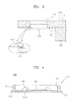
- FIG. 3 is a magnified view of portion A of FIG. 2
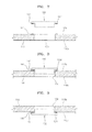
- FIG. 4 is a cross-sectional view of a light-emitting diode package of the electronic component of FIG. 2 .
- the electronic component 100 includes a printed circuit board (PCB) 110, a light-emitting diode package 120, and a plurality of passive devices 130.
- PCB printed circuit board
- the electronic component 100 includes a printed circuit board (PCB) 110, a light-emitting diode package 120, and a plurality of passive devices 130.
- the PCB 110 constitutes a base unit of the electronic component 100, and semiconductor devices, such as diode packages or image sensors, or the passive devices 130, such as capacitors or connectors, are disposed thereon.
- the PCB 110 may be a rigid flexible-printed circuit board (RF-PCB).
- RF-PCB rigid flexible-printed circuit board
- a through-hole 110c is formed in at least a portion, and more particularly, in a region of the PCB 110 where the light-emitting diode package 120 is formed, and this will be described in detail below.
- the PCB 110 includes a first surface 110a and a second surface 110b.
- the first surface 110a and the second surface 110b are opposite surfaces of the PCB 110.
- the first surface 110a is a surface on which the light-emitting diode package 120 and the passive devices 130 are disposed, or mounted, and the second surface 110b is an opposite side relative to the first surface 110a.
- an aspect of the present invention is that the light-emitting diode package 120 and the passive devices 130 are disposed (or mounted) only on the first surface 110a of the PCB 110, and no components are mounted on the second surface 110b of the PCB 110 according to an embodiment of the present invention. This will be described in detail below.
- the light-emitting diode package 120 includes a package main body 121 and a light-emitting diode chip 122 which is seated on the package main body 121.
- the package main body 121 includes a lead frame 121d and a molding unit 121e.
- the lead frame 121d is formed of a metal having electrical conductivity, and includes an anode lead and a cathode lead separated from each other.
- the light-emitting diode chip 122 is disposed on a surface of the lead frame 121d.
- the light-emitting diode chip 122 is electrically connected to the lead frame 121d by a wire 123.
- the molding unit 121e fixes the lead frame 121d.
- the molding unit 121e may be formed of a light resin material and forms a reflection surface 121c.
- the reflection surface 121c is formed by the molding unit 121e.
- the present invention is not limited thereto. That is, the reflection surface 121c may be formed by bending the lead frame 121d.
- the molding unit 121e may further include a protrusion unit 121f.
- a second adhesive member 142 (refer to FIG. 3 ) may be disposed on the protrusion unit 121f so as to be combined with a first adhesive member 141 (refer to FIG. 3 ) disposed on the PCB 110 (refer to FIG. 2 ).
- the protrusion unit 121f protrudes from the molding unit 121e.
- the present invention is not limited thereto. That is, the protrusion unit 121f may protrude from the lead frame 121d.
- the protrusion unit 121f, or protrusions therefore provide terminals to allow the light-emitting diode package 120 to be connected to the PCB.
- the light-emitting diode package 120 and the passive devices 130 are mounted on a surface of the PCB 110 (see FIG. 2 ).
- the surface mount technology is a method of mounting surface mounted components (SMC) which can be directly mounted on the surface of a PCB.
- the light-emitting diode package 120 and the passive devices 130 are mounted only on one surface of the PCB 110.
- the light-emitting diode package 20 is disposed on an upper surface of the PCB 10, and the passive devices 30, such as capacitors or connectors, are disposed on a lower surface of the PCB 10.
- the passive devices 30, such as capacitors or connectors are disposed on a lower surface of the PCB 10.
- the electronic component 100 of FIG. 2 includes the PCB 110 having first surface 110a, second surface 110b, and the predetermined through-hole 110c, and the light-emitting diode package 120 is mounted on a region where the through-hole 110c is formed.
- the first surface 110a of the PCB 110 and the light-emitting diode package 120 are combined with each other, and at the same time, the passive devices 130 are disposed on the first surface 110a of the PCB 110. That is, the combining of the components is performed only on the first surface 110a of the PCB 110.
- Combining may describe various methods of connecting the component terminals to one surface of the PCB and/or mounting the component to one surface of the PCB, for example using surface mount technology.
- the first adhesive member 141 and the second adhesive member 142 of FIG. 3 are disposed on the PCB 110 and the light-emitting diode package 120, respectively.
- the first adhesive member 141 and the second adhesive member 142 include solders, and the PCB 110 and the light-emitting diode package 120 may be combined with each other by soldering them.
- soldering denotes a process of welding using a solder to constitute a circuit after a part is mounted on the PCB 110.
- Methods of soldering may be largely divided into two types, flow soldering and reflow soldering.
- Flow soldering includes a manual soldering method in which a PCB is soaked in a molten solder, and the PCB is subsequently taken out from the molten solder, and an automatic soldering method in which soldering is performed by allowing molten solder to flow onto a PCB which is conveyed by a conveyor.
- reflow soldering denotes a method of soldering by applying heat to a PCB in an oven after applying a cream solder to the PCB.
- a soldering process is completed in that, after applying a cream solder to a portion of a PCB to be combined, a component is placed on the PCB, and then the PCB is allowed to pass through a reflow soldering machine.
- the light-emitting diode package 120 is disposed in the through-hole 110c. Also, the light-emitting diode package 120 and the passive devices 130 are mounted only on the first surface 110a of the PCB 110, and are not mounted on the second surface 110b of the PCB 110. Accordingly, the miniaturization and compactness of the electronic component 100 can be easily achieved, and the manufacturing process can be simplified.
- FIG. 5 is a schematic cross-sectional view of a modified version of the electronic component of FIG. 2 .
- the electronic component 100 includes a PCB 110, a light-emitting diode package 120, and passive devices 130.
- the electronic component 100 according to the modified version of the present invention is distinguished from the above embodiment in that a reflection surface 121c' (see FIG. 5 ) is extended so as to have a predetermined degree angle, which will now be described in detail.
- the optical extraction efficiency of the light-emitting diode package 120 may be reduced since an optical extraction angle of light emitted from the light-emitting diode package 120 is narrowed.
- the reflection surface 121c' ( FIG. 5 ) is formed so as to have a predetermined angle with respect to the PCB 110 ( FIG. 2 ).
- the optical extraction angle of light emitted from the light-emitting diode package 120 is increased. In this way, a reduction of optical extraction efficiency of the light-emitting diode package 120 can be prevented.
- FIGS. 6 to 9 are cross-sectional views illustrating a method of manufacturing the electronic component according to an embodiment of the present invention.
- the method includes: forming the through-hole 110c in the PCB 110 ( FIG. 6 ); preparing the light-emitting diode package 120 having the protrusion unit 121f on an outer circumference thereof ( FIG. 7 ); forming an adhesive member 141, 142 at least on the first surface 110a of the PCB 110 and the protrusion unit 121f of the light-emitting diode package 120 ( FIGS. 7 and 8 ); combining the PCB 110 and the light-emitting diode package 120 with each other ( FIG. 8 ); and forming the passive devices 130 on the first surface 110a of the PCB 110 ( FIG. 2 ).
- FIG. 6 shows the operation of forming the through-hole 110c in the PCB 110.
- the through-hole 110c in which the light-emitting diode package 120 (refer to FIG. 2 ) is mounted, is formed in the PCB 110.
- the through-hole 110c may be formed using a conventional press process.
- FIG. 7 shows the operation of preparing the light-emitting diode package 120 having the protrusion unit 121f on an outer circumference thereof, and forming adhesive members 141 and 142 at least on the first surface 110a of the PCB 110 and on the protrusion unit 121f of the light-emitting diode package 120, respectively.
- the protrusion unit 121f is formed on an outer circumference of the light-emitting diode package 120.
- the second adhesive member 142 may be formed on the protrusion unit 121f.
- the first adhesive member 141 may be formed on a location of the PCB 110 corresponding to the protrusion unit 121f.
- the PCB 110 may be turned over so that the first surface 110a faces upward and the second surface 110b faces downward, as shown in FIG. 7 .
- the first adhesive member 141 is formed on the first surface 110a of the PCB 110 and the second adhesive member 142 is formed on the protrusion unit 121f of the light-emitting diode package 120.
- the present invention is not limited thereto. That is, the adhesive members may not necessarily be included on both the PCB 110 and the light-emitting diode package 120, but may be included only on one of the PCB 110 and the light-emitting diode package 120.
- FIG. 8 shows the operation of combining the PCB 110 and the light-emitting diode package 120.
- the first adhesive member 141 and the second adhesive member 142 respectively include solders, and thus the PCB 110 and the light-emitting diode package 120 may be combined with each other by soldering them. At this point, most of the light-emitting diode package 120 is mounted in the through-hole 110c, and thus, miniaturization and compactness of products can be achieved.
- the method may further include forming the passive devices 130 on the first surface 110a of the PCB 110. That is, as shown in FIG. 8 , in a combined state of the PCB 110 and the light-emitting diode package 120, the passive devices 130 may be disposed on the first surface 110a of the PCB 110 without the need to turn over the PCB 110 in order to change the positions of the first surface 110a and the second surface 110b of the PCB 110. In this way, by allowing the light-emitting diode package 120 and the passive devices 130 to be mounted on the same surface of the PCB 110, the process of manufacturing the electronic component 100 can be simplified.
- the present invention is not limited thereto, that is, the light-emitting diode package 120 and the passive devices 130 may be combined with the PCB 110 through a single soldering operation in a state wherein the light-emitting diode package 120 and the passive devices 130 are disposed together on the PCB 110.
- miniaturization and compactness of an electronic component can be achieved, and the method of manufacturing the electronic component is simplified.
Landscapes
- Engineering & Computer Science (AREA)
- Microelectronics & Electronic Packaging (AREA)
- Manufacturing & Machinery (AREA)
- Led Device Packages (AREA)
- Structures For Mounting Electric Components On Printed Circuit Boards (AREA)
Abstract
Description
- The present invention relates to an electronic component and a method of manufacturing the same, and more particularly, to an electronic component which can be easily miniaturized and made compact, and can be easily manufactured in a simple process, and a method of manufacturing the same.
- Recently, due to the miniaturization and light weight of electronic components, techniques for mounting semiconductor devices such as light-emitting diode packages or image sensors, and passive devices such as capacitors or connectors, on a printed circuit board (PCB) have been developed.
- When electronic components, for example, key pads of mobile phones, are manufactured, passive devices such as capacitors or connectors are generally mounted on a rear surface of a PCB. However, when key buttons are pressed, light must be emitted to a front surface of a mobile phone. Therefore, a light-emitting diode is generally mounted on a front surface of the PCB.
- In a conventional method of manufacturing electronic components, two surface mount technology (SMT) processes are performed with respect to the upper and lower surfaces of a PCB. Thus, a mask for the upper surface and a mask for the lower surface of the PCB are separately required, and this results in increased costs for manufacturing the masks. In addition, since two SMT processes must be performed on the upper and lower surfaces of the PCB, a process of turning over the upper and lower surfaces of the PCB is required. Therefore, the manufacturing process is complicated and takes a long time.
- To address the above and/or other problems, the present invention provides an electronic component which can be readily miniaturized and made compact, and which can be manufactured in a simple process, and a method of manufacturing the same.
- The present invention also provides an electronic component, comprising: a printed circuit board (PCB) having a first surface and a second surface facing each other and a predetermined through-hole; a semiconductor device mounted in the through-hole and combined with the first surface of the PCB; and at least one passive device combined with the first surface of the PCB. The semiconductor device and the passive device(s) may be combined only with the first surface of the PCB.
- The semiconductor device and the passive device(s) may not be combined with the second surface of the PCB.
- The semiconductor device may be a light-emitting diode package.
- The light-emitting diode package may include a protrusion unit disposed at least on an outer circumference thereof, and the protrusion unit is combined with the first surface of the PCB.
- At least an adhesive member may be formed on a surface of the protrusion unit facing the first surface of the PCB, or on the first surface of the PCB, so as to combine the light-emitting diode package with the first surface of the PCB.
- The adhesive member may include a solder.
- The light-emitting diode package may include a package main body and a light-emitting diode chip mounted on the package main body, and the package main body may include a lead frame and a molding unit which fixes the lead frame.
- A surface of the molding unit which surrounds the light-emitting diode chip may be formed so as to have a predetermined angle with respect to the light-emitting diode chip so as to form a reflection surface of light emitted from the light-emitting diode chip.
- The semiconductor device and the passive device(s) may be combined with the PCB using surface mount technology (SMT).
- According to an aspect of the present invention, a method of manufacturing an electronic component comprises the steps of: preparing a PCB having a first surface and a second surface facing each other and a predetermined through-hole; mounting the semiconductor device in the through-hole and combining the semiconductor device with the first surface of the
PCB 110; and combining at least one passive device with the first surface of the PCB. - The semiconductor device may be a light-emitting diode package.
- The light-emitting diode package may include a protrusion unit disposed at least on a portion of an outer circumference thereof, and the step of combining the semiconductor device with the first surface of the PCB may include forming an adhesive member at least on a surface of the protrusion unit facing the first surface of the PCB or on the first surface of the PCB, and soldering the PCB and the light-emitting diode package using the adhesive member.
- The semiconductor device and the passive device(s) may be combined only with the first surface of the PCB.
- The combining of the semiconductor device with the first surface of the PCB and the combining of the passive device(s) with the first surface of the PCB may be performed at the same time.
- According to the present invention, an electronic component can be readily miniaturized and compacted, and a process for manufacturing the electronic component is simple.
- A more complete appreciation of the invention, and many of the attendant advantages thereof, will be readily apparent as the same becomes better understood by reference to the following detailed description when considered in conjunction with the accompanying drawings, in which like reference symbols indicate the same or similar components, wherein:
-
FIG. 1 is a schematic cross-sectional view of an electronic component; -
FIG. 2 is a schematic cross-sectional view of an electronic component according to an embodiment of the present invention; -
FIG. 3 is a magnified view of portion A ofFIG. 2 ; -
FIG. 4 is a cross-sectional view of a light-emitting diode package of the electronic component ofFIG. 2 ; -
FIG. 5 is a schematic cross-sectional view of a modified version of the electronic component ofFIG. 2 ; and -
FIGS. 6 to 9 are cross-sectional views illustrating a method of manufacturing the electronic component according to an embodiment of the present invention. - The present invention will now be described more fully with reference to the accompanying drawings, in which exemplary embodiments of the invention are shown. The invention may, however, be embodied in many different forms and should not be construed as being limited to the embodiments set forth herein. Rather, these embodiments are provided so that this disclosure will be thorough and complete, and will fully convey the concept of the invention to one skilled in the art.
- Like reference numerals are used in the drawings to indicate substantially identical structures or components/parts. Since the drawings are schematically drawn, the relative dimensions and ratios in the drawings are exaggerated or reduced for clarity and convenience.
-
FIG. 1 is a schematic cross-sectional view of an electronic component. - Referring to
FIG. 1 , the electronic component 1 includes a printed circuit board (PCB) 10, a light-emitting diode package 20, andpassive devices 30. - The light-
emitting diode package 20 is disposed on an upper surface of thePCB 10. In this way, in order for the light-emitting diode package 20 to be disposed on the upper surface of thePCB 10, after precisely matching the light-emitting diode package 20 on a region of the upper surface of thePCB 10 where the light-emitting diode package 20 must be combined, a surface mount technology (SMT) process is performed by aligning a molded mask with respect to thePCB 10. - Also, the
passive devices 30, such as capacitors or connectors, are disposed on a lower surface of thePCB 10. In this case, thePCB 10 is turned over so that the lower surface of thePCB 10 faces upward, and an SMT process is subsequently performed by aligning a mold mask with respect to thePCB 10. - In this way, two SMT processes are performed with respect to the upper and lower surfaces of the
PCB 10. Thus, a mask for the upper surface and a mask for the lower surface of thePCB 10 are separately required, and accordingly, costs for manufacturing the masks are increased. In addition, since two SMT processes must be performed on the upper and lower surfaces of thePCB 10, a process of turning over the upper and lower surfaces of thePCB 10 is required. Therefore, the manufacturing process is complicated and takes a long time. -
FIG. 2 is a schematic cross-sectional view of an electronic component according to an embodiment of the present invention,FIG. 3 is a magnified view of portion A ofFIG. 2 , andFIG. 4 is a cross-sectional view of a light-emitting diode package of the electronic component ofFIG. 2 . - Referring to
FIGS. 2 to 4 , theelectronic component 100 includes a printed circuit board (PCB) 110, a light-emitting diode package 120, and a plurality ofpassive devices 130. - The PCB 110 constitutes a base unit of the
electronic component 100, and semiconductor devices, such as diode packages or image sensors, or thepassive devices 130, such as capacitors or connectors, are disposed thereon. The PCB 110 may be a rigid flexible-printed circuit board (RF-PCB). In this regard, it is an aspect of the present invention that a through-hole 110c is formed in at least a portion, and more particularly, in a region of the PCB 110 where the light-emittingdiode package 120 is formed, and this will be described in detail below. - The PCB 110 includes a
first surface 110a and asecond surface 110b. Thefirst surface 110a and thesecond surface 110b are opposite surfaces of the PCB 110. Thefirst surface 110a is a surface on which the light-emitting diode package 120 and thepassive devices 130 are disposed, or mounted, and thesecond surface 110b is an opposite side relative to thefirst surface 110a. In this regard, an aspect of the present invention is that the light-emittingdiode package 120 and thepassive devices 130 are disposed (or mounted) only on thefirst surface 110a of thePCB 110, and no components are mounted on thesecond surface 110b of thePCB 110 according to an embodiment of the present invention. This will be described in detail below. - Referring to
FIG. 4 , which shows the light-emitting diode package 120 of theelectronic component 100, the light-emitting diode package 120 according to an embodiment of the present invention includes a packagemain body 121 and a light-emitting diode chip 122 which is seated on the packagemain body 121. - The package
main body 121 includes alead frame 121d and amolding unit 121e. - The
lead frame 121d is formed of a metal having electrical conductivity, and includes an anode lead and a cathode lead separated from each other. The light-emittingdiode chip 122 is disposed on a surface of thelead frame 121d. The light-emittingdiode chip 122 is electrically connected to thelead frame 121d by awire 123. - The
molding unit 121e fixes thelead frame 121d. Themolding unit 121e may be formed of a light resin material and forms areflection surface 121c. InFIG. 4 , thereflection surface 121c is formed by themolding unit 121e. However, the present invention is not limited thereto. That is, thereflection surface 121c may be formed by bending thelead frame 121d. - The
molding unit 121e may further include aprotrusion unit 121f. Also, a second adhesive member 142 (refer toFIG. 3 ) may be disposed on theprotrusion unit 121f so as to be combined with a first adhesive member 141 (refer toFIG. 3 ) disposed on the PCB 110 (refer toFIG. 2 ). InFIG. 4 , theprotrusion unit 121f protrudes from themolding unit 121e. However, the present invention is not limited thereto. That is, theprotrusion unit 121f may protrude from thelead frame 121d. Theprotrusion unit 121f, or protrusions, therefore provide terminals to allow the light-emittingdiode package 120 to be connected to the PCB. - The light-emitting
diode package 120 and thepassive devices 130 are mounted on a surface of the PCB 110 (seeFIG. 2 ). The surface mount technology (SMT) is a method of mounting surface mounted components (SMC) which can be directly mounted on the surface of a PCB. - In the latter regard, in the
electronic component 100 according to an embodiment of the present invention, it is an aspect that the light-emittingdiode package 120 and thepassive devices 130 are mounted only on one surface of thePCB 110. - As described above with reference to
FIG. 1 , in a method of mounting the electronic component 1, the light-emittingdiode package 20 is disposed on an upper surface of thePCB 10, and thepassive devices 30, such as capacitors or connectors, are disposed on a lower surface of thePCB 10. In this case, in the SMT processes, since a mask for the upper surface of thePCB 10 and a mask for the lower surface of thePCB 10 are needed, the cost of manufacturing masks increases. Moreover, since a total of two SMT processes (that is, on the upper and lower surfaces of the PCB 110) must be performed, the manufacturing process is complicated and takes a long time. - In order to address the above problems, an aspect of the present invention is that the
electronic component 100 ofFIG. 2 includes thePCB 110 havingfirst surface 110a,second surface 110b, and the predetermined through-hole 110c, and the light-emittingdiode package 120 is mounted on a region where the through-hole 110c is formed. In this case, thefirst surface 110a of thePCB 110 and the light-emittingdiode package 120 are combined with each other, and at the same time, thepassive devices 130 are disposed on thefirst surface 110a of thePCB 110. That is, the combining of the components is performed only on thefirst surface 110a of thePCB 110. Combining may describe various methods of connecting the component terminals to one surface of the PCB and/or mounting the component to one surface of the PCB, for example using surface mount technology. - In order to combine the
PCB 110 and the light-emittingdiode package 120, the firstadhesive member 141 and the secondadhesive member 142 ofFIG. 3 are disposed on thePCB 110 and the light-emittingdiode package 120, respectively. The firstadhesive member 141 and the secondadhesive member 142 include solders, and thePCB 110 and the light-emittingdiode package 120 may be combined with each other by soldering them. - In this regard, soldering denotes a process of welding using a solder to constitute a circuit after a part is mounted on the
PCB 110. Methods of soldering may be largely divided into two types, flow soldering and reflow soldering. Flow soldering includes a manual soldering method in which a PCB is soaked in a molten solder, and the PCB is subsequently taken out from the molten solder, and an automatic soldering method in which soldering is performed by allowing molten solder to flow onto a PCB which is conveyed by a conveyor. Also, reflow soldering denotes a method of soldering by applying heat to a PCB in an oven after applying a cream solder to the PCB. That is, a soldering process is completed in that, after applying a cream solder to a portion of a PCB to be combined, a component is placed on the PCB, and then the PCB is allowed to pass through a reflow soldering machine. - In this way, after forming the through-
hole 110c in thePCB 110, the light-emittingdiode package 120 is disposed in the through-hole 110c. Also, the light-emittingdiode package 120 and thepassive devices 130 are mounted only on thefirst surface 110a of thePCB 110, and are not mounted on thesecond surface 110b of thePCB 110. Accordingly, the miniaturization and compactness of theelectronic component 100 can be easily achieved, and the manufacturing process can be simplified. -
FIG. 5 is a schematic cross-sectional view of a modified version of the electronic component ofFIG. 2 . - Referring to
FIG. 2 andFIG. 5 , theelectronic component 100 includes aPCB 110, a light-emittingdiode package 120, andpassive devices 130. Theelectronic component 100 according to the modified version of the present invention is distinguished from the above embodiment in that areflection surface 121c' (seeFIG. 5 ) is extended so as to have a predetermined degree angle, which will now be described in detail. - In the case wherein the light-emitting
diode package 120 is mounted in the through-hole 110c of thePCB 110 as shown inFIG. 2 , the optical extraction efficiency of the light-emittingdiode package 120 may be reduced since an optical extraction angle of light emitted from the light-emittingdiode package 120 is narrowed. In order to address this problem, in theelectronic component 100 according to the modified version of the present invention, thereflection surface 121c' (FIG. 5 ) is formed so as to have a predetermined angle with respect to the PCB 110 (FIG. 2 ). Thus, the optical extraction angle of light emitted from the light-emittingdiode package 120 is increased. In this way, a reduction of optical extraction efficiency of the light-emittingdiode package 120 can be prevented. - A method of manufacturing the
electronic component 100, according to an embodiment of the present invention, will now be described. -
FIGS. 6 to 9 are cross-sectional views illustrating a method of manufacturing the electronic component according to an embodiment of the present invention. - Referring to
FIGS. 6 to 9 , in the method of manufacturing theelectronic component 100, the method includes: forming the through-hole 110c in the PCB 110 (FIG. 6 ); preparing the light-emittingdiode package 120 having theprotrusion unit 121f on an outer circumference thereof (FIG. 7 ); forming anadhesive member first surface 110a of thePCB 110 and theprotrusion unit 121f of the light-emitting diode package 120 (FIGS. 7 and 8 ); combining thePCB 110 and the light-emittingdiode package 120 with each other (FIG. 8 ); and forming thepassive devices 130 on thefirst surface 110a of the PCB 110 (FIG. 2 ). -
FIG. 6 shows the operation of forming the through-hole 110c in thePCB 110. As shown inFIG. 6 , the through-hole 110c, in which the light-emitting diode package 120 (refer toFIG. 2 ) is mounted, is formed in thePCB 110. The through-hole 110c may be formed using a conventional press process. -
FIG. 7 shows the operation of preparing the light-emittingdiode package 120 having theprotrusion unit 121f on an outer circumference thereof, and formingadhesive members first surface 110a of thePCB 110 and on theprotrusion unit 121f of the light-emittingdiode package 120, respectively. - As shown in
FIG. 7 , theprotrusion unit 121f is formed on an outer circumference of the light-emittingdiode package 120. The secondadhesive member 142 may be formed on theprotrusion unit 121f. In addition, the firstadhesive member 141 may be formed on a location of thePCB 110 corresponding to theprotrusion unit 121f. At this point, in order to facilitate the combining of thePCB 110 and the light-emittingdiode package 120, thePCB 110 may be turned over so that thefirst surface 110a faces upward and thesecond surface 110b faces downward, as shown inFIG. 7 . - In
FIG. 7 , it is depicted that the firstadhesive member 141 is formed on thefirst surface 110a of thePCB 110 and the secondadhesive member 142 is formed on theprotrusion unit 121f of the light-emittingdiode package 120. However, the present invention is not limited thereto. That is, the adhesive members may not necessarily be included on both thePCB 110 and the light-emittingdiode package 120, but may be included only on one of thePCB 110 and the light-emittingdiode package 120. -
FIG. 8 shows the operation of combining thePCB 110 and the light-emittingdiode package 120. As described above, the firstadhesive member 141 and the secondadhesive member 142 respectively include solders, and thus thePCB 110 and the light-emittingdiode package 120 may be combined with each other by soldering them. At this point, most of the light-emittingdiode package 120 is mounted in the through-hole 110c, and thus, miniaturization and compactness of products can be achieved. - Next, although not shown in
FIG. 9 , the method may further include forming thepassive devices 130 on thefirst surface 110a of thePCB 110. That is, as shown inFIG. 8 , in a combined state of thePCB 110 and the light-emittingdiode package 120, thepassive devices 130 may be disposed on thefirst surface 110a of thePCB 110 without the need to turn over thePCB 110 in order to change the positions of thefirst surface 110a and thesecond surface 110b of thePCB 110. In this way, by allowing the light-emittingdiode package 120 and thepassive devices 130 to be mounted on the same surface of thePCB 110, the process of manufacturing theelectronic component 100 can be simplified. - In the drawings, it is depicted that the combination of the light-emitting
diode package 120 with thePCB 110, and the combination of thepassive devices 130 with thePCB 110, are sequentially performed. However, the present invention is not limited thereto, that is, the light-emittingdiode package 120 and thepassive devices 130 may be combined with thePCB 110 through a single soldering operation in a state wherein the light-emittingdiode package 120 and thepassive devices 130 are disposed together on thePCB 110. - Finally, when the
first surface 110a and thesecond surface 110b of thePCB 110 are turned over, the manufacture of theelectronic component 100, as shown inFIG. 9 , is completed. - According to the present invention, miniaturization and compactness of an electronic component can be achieved, and the method of manufacturing the electronic component is simplified.
- While the present invention has been particularly shown and described with reference to exemplary embodiments thereof, it will be understood by one of ordinary skill in the art that various changes in form and detail may be made therein without departing from the scope of the present invention as defined by the following claims.
Claims (13)
- An electronic component (100), comprising:a printed circuit board PCB (110) having a through-hole (110c);a semiconductor device (120) mounted in the through-hole and combined with a first surface of the PCB; andat least one passive device combined with the first surface of the PCB.
- The electronic component of claim 1, wherein the semiconductor device and the passive devices are combined only with the first surface of the PCB.
- The electronic component of claim 1 or 2, wherein the semiconductor device and the passive devices are not combined with a second surface of the PCB opposite the first surface.
- The electronic component of any one of the preceding claims, wherein the semiconductor device comprises a light-emitting diode package.
- The electronic component of claim 4, wherein the light-emitting diode package comprises a protrusion unit on at least an outer circumference of the light-emitting diode package, wherein the protrusion unit is combined with the first surface of the PCB.
- The electronic component of claim 5, wherein an adhesive member is formed on one of a surface of the protrusion unit facing the first surface of the PCB and the first surface of the PCB so as to combine the light-emitting diode package with the first surface of the PCB.
- The electronic component of claim 6, wherein the adhesive member comprises a solder.
- The electronic component of claim 4, wherein the light-emitting diode package comprises a package main body and a light-emitting diode chip mounted on the package main body, and wherein the package main body comprises a lead frame and a molding unit which fixes the lead frame.
- The electronic component of claim 8, wherein a surface of the molding unit which surrounds the light-emitting diode chip is formed so as to have a predetermined angle with respect to the light-emitting diode chip so as to form a reflection surface for light emitted from the light-emitting diode chip.
- The electronic component of any one of the preceding claims, wherein the semiconductor device and the passive devices are combined with the PCB using surface mount technology (SMT).
- A method of manufacturing an electronic component, the method comprising the steps of:preparing a printed circuit board PCB having a first surface and a through-hole;mounting the semiconductor device in the through-hole and combining the semiconductor device with the first surface of the PCB; andcombining passive devices with the first surface of the PCB.
- The method of claim 11, wherein the semiconductor device comprises a light-emitting diode package and the light-emitting diode package comprises a protrusion unit on at least a portion of an outer circumference of the light-emitting diode package, wherein the step of combining the semiconductor device with the first surface of the PCB comprises:forming an adhesive member on one of a surface of the protrusion unit facing the first surface of the PCB and the first surface of the PCB; andsoldering the PCB and the light-emitting diode package using the adhesive member.
- The method of claim 11 or 12, wherein the step of combining the semiconductor device with the first surface of the PCB and the step of combining the passive devices with the first surface of the PCB are performed at the same time.
Applications Claiming Priority (1)
| Application Number | Priority Date | Filing Date | Title |
|---|---|---|---|
| KR1020100084177A KR101677105B1 (en) | 2010-08-30 | 2010-08-30 | Electronic component and manufacturing method for the same |
Publications (2)
| Publication Number | Publication Date |
|---|---|
| EP2424339A1 true EP2424339A1 (en) | 2012-02-29 |
| EP2424339B1 EP2424339B1 (en) | 2017-11-15 |
Family
ID=44534010
Family Applications (1)
| Application Number | Title | Priority Date | Filing Date |
|---|---|---|---|
| EP11178699.2A Active EP2424339B1 (en) | 2010-08-30 | 2011-08-24 | Electronic component and method of manufacturing the same |
Country Status (5)
| Country | Link |
|---|---|
| US (1) | US20120051017A1 (en) |
| EP (1) | EP2424339B1 (en) |
| JP (1) | JP2012049527A (en) |
| KR (1) | KR101677105B1 (en) |
| CN (1) | CN102387663A (en) |
Families Citing this family (14)
| Publication number | Priority date | Publication date | Assignee | Title |
|---|---|---|---|---|
| KR101245632B1 (en) * | 2011-08-30 | 2013-03-20 | 주식회사 인지모바일솔루션 | Led package and its manufacturing method |
| CN103515366A (en) * | 2012-06-15 | 2014-01-15 | 霍尼韦尔朗能电器系统技术(广东)有限公司 | LED integrated light source and connecting method thereof |
| JP6483352B2 (en) * | 2014-05-09 | 2019-03-13 | 株式会社小糸製作所 | LED unit and manufacturing method thereof |
| CN107978596B (en) * | 2016-10-24 | 2020-05-12 | 光宝光电(常州)有限公司 | Optical sensor module and wearable device thereof |
| TWI656632B (en) * | 2017-05-12 | 2019-04-11 | 海華科技股份有限公司 | Portable electronic device and image-capturing module thereof, and carrier assembly thereof |
| CN109756109A (en) * | 2017-11-02 | 2019-05-14 | 北京嘉楠捷思信息技术有限公司 | Switching voltage reduction power supply and heat dissipation system thereof |
| DE102017130342A1 (en) * | 2017-12-18 | 2019-06-19 | Melexis Bulgaria Ltd. | Reinforced electronic device for an electric motor |
| CN110473839B (en) | 2018-05-11 | 2025-03-21 | 三星电子株式会社 | Semiconductor packaging system |
| US10991638B2 (en) | 2018-05-14 | 2021-04-27 | Samsung Electronics Co., Ltd. | Semiconductor package system |
| US11244885B2 (en) | 2018-09-18 | 2022-02-08 | Samsung Electronics Co., Ltd. | Semiconductor package system |
| US11600607B2 (en) | 2019-01-17 | 2023-03-07 | Samsung Electronics Co., Ltd. | Semiconductor module including multiple power management semiconductor packages |
| KR102223428B1 (en) * | 2019-07-03 | 2021-03-05 | 한국과학기술원 | Insert type transparent led display and production method thereof |
| KR102843210B1 (en) | 2020-10-05 | 2025-08-05 | 삼성전자주식회사 | Display apparatus |
| CN115616815B (en) * | 2022-09-01 | 2024-03-22 | 厦门天马微电子有限公司 | Backlight module, display device and preparation method of backlight module |
Citations (2)
| Publication number | Priority date | Publication date | Assignee | Title |
|---|---|---|---|---|
| US20070081323A1 (en) * | 2005-10-12 | 2007-04-12 | Samsung Electro-Mechanics Co., Ltd. | Led backlight unit |
| US20090126980A1 (en) * | 2007-11-07 | 2009-05-21 | Eiji Katsuta | Printed wiring board |
Family Cites Families (9)
| Publication number | Priority date | Publication date | Assignee | Title |
|---|---|---|---|---|
| DE10020465A1 (en) * | 2000-04-26 | 2001-11-08 | Osram Opto Semiconductors Gmbh | Radiation-emitting semiconductor component with luminescence conversion element |
| DE10117889A1 (en) * | 2001-04-10 | 2002-10-24 | Osram Opto Semiconductors Gmbh | Leadframe used for a light emitting diode component comprises a chip assembly region, a wire connecting region, external electrical connecting strips, and a support part coupled with a thermal connecting part |
| US20040264195A1 (en) * | 2003-06-25 | 2004-12-30 | Chia-Fu Chang | Led light source having a heat sink |
| US20050077616A1 (en) * | 2003-10-09 | 2005-04-14 | Ng Kee Yean | High power light emitting diode device |
| TWM271255U (en) * | 2004-10-08 | 2005-07-21 | Bright Led Electronics Corp | High-power surface-mounted light-emitting diode with high heat dissipation property |
| JP4870509B2 (en) * | 2006-09-27 | 2012-02-08 | 新光電気工業株式会社 | Electronic equipment |
| JP2010272744A (en) * | 2009-05-22 | 2010-12-02 | Kyushu Institute Of Technology | LED module device and manufacturing method thereof |
| JP2011159951A (en) * | 2010-01-07 | 2011-08-18 | Kyushu Institute Of Technology | Led module device and method of manufacturing the same |
| KR20100089055A (en) * | 2010-07-23 | 2010-08-11 | 주식회사 루멘스 | Light emitting diode package |
-
2010
- 2010-08-30 KR KR1020100084177A patent/KR101677105B1/en active Active
-
2011
- 2011-02-02 US US13/019,370 patent/US20120051017A1/en not_active Abandoned
- 2011-08-04 JP JP2011170978A patent/JP2012049527A/en not_active Ceased
- 2011-08-24 EP EP11178699.2A patent/EP2424339B1/en active Active
- 2011-08-30 CN CN2011102599220A patent/CN102387663A/en active Pending
Patent Citations (2)
| Publication number | Priority date | Publication date | Assignee | Title |
|---|---|---|---|---|
| US20070081323A1 (en) * | 2005-10-12 | 2007-04-12 | Samsung Electro-Mechanics Co., Ltd. | Led backlight unit |
| US20090126980A1 (en) * | 2007-11-07 | 2009-05-21 | Eiji Katsuta | Printed wiring board |
Also Published As
| Publication number | Publication date |
|---|---|
| US20120051017A1 (en) | 2012-03-01 |
| EP2424339B1 (en) | 2017-11-15 |
| JP2012049527A (en) | 2012-03-08 |
| CN102387663A (en) | 2012-03-21 |
| KR101677105B1 (en) | 2016-11-17 |
| KR20120020521A (en) | 2012-03-08 |
Similar Documents
| Publication | Publication Date | Title |
|---|---|---|
| EP2424339A1 (en) | Electronic component and method of manufacturing the same | |
| US6862804B2 (en) | Method of mounting camera module on wiring board | |
| TWI590425B (en) | An optoelectronic module including an electrically conductive connection for integration with an electronic device | |
| EP1646271A3 (en) | Control device and method of manufacturing thereof | |
| CN110351467B (en) | Camera module, electronic equipment and manufacturing method of camera module | |
| KR20070078169A (en) | Light emitting diode package and manufacturing method thereof | |
| JP3205631U (en) | VEHICLE LIGHT DEVICE AND LIGHT EMITTING MODULE THEREOF | |
| US7881067B2 (en) | Circuit board assembly | |
| KR20150126778A (en) | Board integrated interconnect | |
| US9942988B2 (en) | Circuit board and power supply apparatus | |
| JP2016082074A (en) | Electrical device and method of manufacturing the same | |
| EP2134146A1 (en) | Printed circuit board assembly and a method of assembling thereof | |
| WO2007100173A1 (en) | Multi-layer package structure and fabrication method thereof | |
| KR101974920B1 (en) | Bonded structural body between PCBs | |
| JP2006295038A (en) | Manufacturing method of three-dimensionally configured electronic circuit unit | |
| KR100538145B1 (en) | Module with different boards and method for assembly the module | |
| KR100691995B1 (en) | SMT speaker structure of mobile communication terminal and its method | |
| CN101005170A (en) | Plate-to-plate connection structure | |
| KR101208875B1 (en) | Printed circuit board mounting process | |
| EP4021153A1 (en) | Electronic circuit device and manufacturing method of same | |
| KR101175879B1 (en) | Camera Module And Manufacturing Method Thereof | |
| KR100656662B1 (en) | Light emitting device package and its manufacturing method | |
| KR100927423B1 (en) | Glass cap molding package and manufacturing method thereof, and camera module | |
| KR200358680Y1 (en) | Doom Swich Sturcture for Electronic Equipment Key Pad | |
| JP2010258295A (en) | High frequency module, manufacturing method thereof, and electronic device |
Legal Events
| Date | Code | Title | Description |
|---|---|---|---|
| AK | Designated contracting states |
Kind code of ref document: A1 Designated state(s): AL AT BE BG CH CY CZ DE DK EE ES FI FR GB GR HR HU IE IS IT LI LT LU LV MC MK MT NL NO PL PT RO RS SE SI SK SM TR |
|
| AX | Request for extension of the european patent |
Extension state: BA ME |
|
| PUAI | Public reference made under article 153(3) epc to a published international application that has entered the european phase |
Free format text: ORIGINAL CODE: 0009012 |
|
| 17P | Request for examination filed |
Effective date: 20120229 |
|
| RAP1 | Party data changed (applicant data changed or rights of an application transferred) |
Owner name: SAMSUNG DISPLAY CO., LTD. |
|
| 17Q | First examination report despatched |
Effective date: 20140221 |
|
| RAP1 | Party data changed (applicant data changed or rights of an application transferred) |
Owner name: SAMSUNG DISPLAY CO., LTD. |
|
| GRAP | Despatch of communication of intention to grant a patent |
Free format text: ORIGINAL CODE: EPIDOSNIGR1 |
|
| STAA | Information on the status of an ep patent application or granted ep patent |
Free format text: STATUS: GRANT OF PATENT IS INTENDED |
|
| INTG | Intention to grant announced |
Effective date: 20170526 |
|
| GRAS | Grant fee paid |
Free format text: ORIGINAL CODE: EPIDOSNIGR3 |
|
| GRAA | (expected) grant |
Free format text: ORIGINAL CODE: 0009210 |
|
| STAA | Information on the status of an ep patent application or granted ep patent |
Free format text: STATUS: THE PATENT HAS BEEN GRANTED |
|
| AK | Designated contracting states |
Kind code of ref document: B1 Designated state(s): AL AT BE BG CH CY CZ DE DK EE ES FI FR GB GR HR HU IE IS IT LI LT LU LV MC MK MT NL NO PL PT RO RS SE SI SK SM TR |
|
| REG | Reference to a national code |
Ref country code: AT Ref legal event code: REF Ref document number: 947487 Country of ref document: AT Kind code of ref document: T Effective date: 20171115 Ref country code: GB Ref legal event code: FG4D Ref country code: CH Ref legal event code: EP |
|
| REG | Reference to a national code |
Ref country code: IE Ref legal event code: FG4D |
|
| REG | Reference to a national code |
Ref country code: DE Ref legal event code: R096 Ref document number: 602011043306 Country of ref document: DE |
|
| REG | Reference to a national code |
Ref country code: NL Ref legal event code: FP |
|
| REG | Reference to a national code |
Ref country code: LT Ref legal event code: MG4D |
|
| REG | Reference to a national code |
Ref country code: AT Ref legal event code: MK05 Ref document number: 947487 Country of ref document: AT Kind code of ref document: T Effective date: 20171115 |
|
| PG25 | Lapsed in a contracting state [announced via postgrant information from national office to epo] |
Ref country code: SE Free format text: LAPSE BECAUSE OF FAILURE TO SUBMIT A TRANSLATION OF THE DESCRIPTION OR TO PAY THE FEE WITHIN THE PRESCRIBED TIME-LIMIT Effective date: 20171115 Ref country code: ES Free format text: LAPSE BECAUSE OF FAILURE TO SUBMIT A TRANSLATION OF THE DESCRIPTION OR TO PAY THE FEE WITHIN THE PRESCRIBED TIME-LIMIT Effective date: 20171115 Ref country code: LT Free format text: LAPSE BECAUSE OF FAILURE TO SUBMIT A TRANSLATION OF THE DESCRIPTION OR TO PAY THE FEE WITHIN THE PRESCRIBED TIME-LIMIT Effective date: 20171115 Ref country code: FI Free format text: LAPSE BECAUSE OF FAILURE TO SUBMIT A TRANSLATION OF THE DESCRIPTION OR TO PAY THE FEE WITHIN THE PRESCRIBED TIME-LIMIT Effective date: 20171115 Ref country code: NO Free format text: LAPSE BECAUSE OF FAILURE TO SUBMIT A TRANSLATION OF THE DESCRIPTION OR TO PAY THE FEE WITHIN THE PRESCRIBED TIME-LIMIT Effective date: 20180215 |
|
| PG25 | Lapsed in a contracting state [announced via postgrant information from national office to epo] |
Ref country code: AT Free format text: LAPSE BECAUSE OF FAILURE TO SUBMIT A TRANSLATION OF THE DESCRIPTION OR TO PAY THE FEE WITHIN THE PRESCRIBED TIME-LIMIT Effective date: 20171115 Ref country code: RS Free format text: LAPSE BECAUSE OF FAILURE TO SUBMIT A TRANSLATION OF THE DESCRIPTION OR TO PAY THE FEE WITHIN THE PRESCRIBED TIME-LIMIT Effective date: 20171115 Ref country code: HR Free format text: LAPSE BECAUSE OF FAILURE TO SUBMIT A TRANSLATION OF THE DESCRIPTION OR TO PAY THE FEE WITHIN THE PRESCRIBED TIME-LIMIT Effective date: 20171115 Ref country code: GR Free format text: LAPSE BECAUSE OF FAILURE TO SUBMIT A TRANSLATION OF THE DESCRIPTION OR TO PAY THE FEE WITHIN THE PRESCRIBED TIME-LIMIT Effective date: 20180216 Ref country code: LV Free format text: LAPSE BECAUSE OF FAILURE TO SUBMIT A TRANSLATION OF THE DESCRIPTION OR TO PAY THE FEE WITHIN THE PRESCRIBED TIME-LIMIT Effective date: 20171115 Ref country code: BG Free format text: LAPSE BECAUSE OF FAILURE TO SUBMIT A TRANSLATION OF THE DESCRIPTION OR TO PAY THE FEE WITHIN THE PRESCRIBED TIME-LIMIT Effective date: 20180215 |
|
| REG | Reference to a national code |
Ref country code: FR Ref legal event code: PLFP Year of fee payment: 8 |
|
| PG25 | Lapsed in a contracting state [announced via postgrant information from national office to epo] |
Ref country code: CZ Free format text: LAPSE BECAUSE OF FAILURE TO SUBMIT A TRANSLATION OF THE DESCRIPTION OR TO PAY THE FEE WITHIN THE PRESCRIBED TIME-LIMIT Effective date: 20171115 Ref country code: CY Free format text: LAPSE BECAUSE OF FAILURE TO SUBMIT A TRANSLATION OF THE DESCRIPTION OR TO PAY THE FEE WITHIN THE PRESCRIBED TIME-LIMIT Effective date: 20171115 Ref country code: DK Free format text: LAPSE BECAUSE OF FAILURE TO SUBMIT A TRANSLATION OF THE DESCRIPTION OR TO PAY THE FEE WITHIN THE PRESCRIBED TIME-LIMIT Effective date: 20171115 Ref country code: EE Free format text: LAPSE BECAUSE OF FAILURE TO SUBMIT A TRANSLATION OF THE DESCRIPTION OR TO PAY THE FEE WITHIN THE PRESCRIBED TIME-LIMIT Effective date: 20171115 Ref country code: SK Free format text: LAPSE BECAUSE OF FAILURE TO SUBMIT A TRANSLATION OF THE DESCRIPTION OR TO PAY THE FEE WITHIN THE PRESCRIBED TIME-LIMIT Effective date: 20171115 |
|
| REG | Reference to a national code |
Ref country code: DE Ref legal event code: R097 Ref document number: 602011043306 Country of ref document: DE |
|
| PG25 | Lapsed in a contracting state [announced via postgrant information from national office to epo] |
Ref country code: RO Free format text: LAPSE BECAUSE OF FAILURE TO SUBMIT A TRANSLATION OF THE DESCRIPTION OR TO PAY THE FEE WITHIN THE PRESCRIBED TIME-LIMIT Effective date: 20171115 Ref country code: IT Free format text: LAPSE BECAUSE OF FAILURE TO SUBMIT A TRANSLATION OF THE DESCRIPTION OR TO PAY THE FEE WITHIN THE PRESCRIBED TIME-LIMIT Effective date: 20171115 Ref country code: SM Free format text: LAPSE BECAUSE OF FAILURE TO SUBMIT A TRANSLATION OF THE DESCRIPTION OR TO PAY THE FEE WITHIN THE PRESCRIBED TIME-LIMIT Effective date: 20171115 Ref country code: PL Free format text: LAPSE BECAUSE OF FAILURE TO SUBMIT A TRANSLATION OF THE DESCRIPTION OR TO PAY THE FEE WITHIN THE PRESCRIBED TIME-LIMIT Effective date: 20171115 |
|
| PLBE | No opposition filed within time limit |
Free format text: ORIGINAL CODE: 0009261 |
|
| STAA | Information on the status of an ep patent application or granted ep patent |
Free format text: STATUS: NO OPPOSITION FILED WITHIN TIME LIMIT |
|
| 26N | No opposition filed |
Effective date: 20180817 |
|
| PG25 | Lapsed in a contracting state [announced via postgrant information from national office to epo] |
Ref country code: SI Free format text: LAPSE BECAUSE OF FAILURE TO SUBMIT A TRANSLATION OF THE DESCRIPTION OR TO PAY THE FEE WITHIN THE PRESCRIBED TIME-LIMIT Effective date: 20171115 |
|
| PG25 | Lapsed in a contracting state [announced via postgrant information from national office to epo] |
Ref country code: MC Free format text: LAPSE BECAUSE OF FAILURE TO SUBMIT A TRANSLATION OF THE DESCRIPTION OR TO PAY THE FEE WITHIN THE PRESCRIBED TIME-LIMIT Effective date: 20171115 |
|
| REG | Reference to a national code |
Ref country code: CH Ref legal event code: PL |
|
| PG25 | Lapsed in a contracting state [announced via postgrant information from national office to epo] |
Ref country code: LI Free format text: LAPSE BECAUSE OF NON-PAYMENT OF DUE FEES Effective date: 20180831 Ref country code: LU Free format text: LAPSE BECAUSE OF NON-PAYMENT OF DUE FEES Effective date: 20180824 Ref country code: CH Free format text: LAPSE BECAUSE OF NON-PAYMENT OF DUE FEES Effective date: 20180831 |
|
| REG | Reference to a national code |
Ref country code: BE Ref legal event code: MM Effective date: 20180831 |
|
| PG25 | Lapsed in a contracting state [announced via postgrant information from national office to epo] |
Ref country code: BE Free format text: LAPSE BECAUSE OF NON-PAYMENT OF DUE FEES Effective date: 20180831 |
|
| PG25 | Lapsed in a contracting state [announced via postgrant information from national office to epo] |
Ref country code: MT Free format text: LAPSE BECAUSE OF NON-PAYMENT OF DUE FEES Effective date: 20180824 |
|
| PG25 | Lapsed in a contracting state [announced via postgrant information from national office to epo] |
Ref country code: TR Free format text: LAPSE BECAUSE OF FAILURE TO SUBMIT A TRANSLATION OF THE DESCRIPTION OR TO PAY THE FEE WITHIN THE PRESCRIBED TIME-LIMIT Effective date: 20171115 |
|
| PG25 | Lapsed in a contracting state [announced via postgrant information from national office to epo] |
Ref country code: HU Free format text: LAPSE BECAUSE OF FAILURE TO SUBMIT A TRANSLATION OF THE DESCRIPTION OR TO PAY THE FEE WITHIN THE PRESCRIBED TIME-LIMIT; INVALID AB INITIO Effective date: 20110824 Ref country code: PT Free format text: LAPSE BECAUSE OF FAILURE TO SUBMIT A TRANSLATION OF THE DESCRIPTION OR TO PAY THE FEE WITHIN THE PRESCRIBED TIME-LIMIT Effective date: 20171115 |
|
| PG25 | Lapsed in a contracting state [announced via postgrant information from national office to epo] |
Ref country code: IE Free format text: LAPSE BECAUSE OF NON-PAYMENT OF DUE FEES Effective date: 20180824 Ref country code: MK Free format text: LAPSE BECAUSE OF NON-PAYMENT OF DUE FEES Effective date: 20171115 |
|
| PG25 | Lapsed in a contracting state [announced via postgrant information from national office to epo] |
Ref country code: IS Free format text: LAPSE BECAUSE OF FAILURE TO SUBMIT A TRANSLATION OF THE DESCRIPTION OR TO PAY THE FEE WITHIN THE PRESCRIBED TIME-LIMIT Effective date: 20180315 Ref country code: AL Free format text: LAPSE BECAUSE OF FAILURE TO SUBMIT A TRANSLATION OF THE DESCRIPTION OR TO PAY THE FEE WITHIN THE PRESCRIBED TIME-LIMIT Effective date: 20171115 |
|
| P01 | Opt-out of the competence of the unified patent court (upc) registered |
Effective date: 20230515 |
|
| PGFP | Annual fee paid to national office [announced via postgrant information from national office to epo] |
Ref country code: NL Payment date: 20250722 Year of fee payment: 15 |
|
| PGFP | Annual fee paid to national office [announced via postgrant information from national office to epo] |
Ref country code: DE Payment date: 20250721 Year of fee payment: 15 |
|
| PGFP | Annual fee paid to national office [announced via postgrant information from national office to epo] |
Ref country code: GB Payment date: 20250722 Year of fee payment: 15 |
|
| PGFP | Annual fee paid to national office [announced via postgrant information from national office to epo] |
Ref country code: FR Payment date: 20250725 Year of fee payment: 15 |