EP2422447B1 - Elektronische schaltungen mit einem mosfet und einem dual-gate-jfet - Google Patents
Elektronische schaltungen mit einem mosfet und einem dual-gate-jfet Download PDFInfo
- Publication number
- EP2422447B1 EP2422447B1 EP10767521.7A EP10767521A EP2422447B1 EP 2422447 B1 EP2422447 B1 EP 2422447B1 EP 10767521 A EP10767521 A EP 10767521A EP 2422447 B1 EP2422447 B1 EP 2422447B1
- Authority
- EP
- European Patent Office
- Prior art keywords
- gate
- jfet
- mosfet
- voltage
- coupled
- Prior art date
- Legal status (The legal status is an assumption and is not a legal conclusion. Google has not performed a legal analysis and makes no representation as to the accuracy of the status listed.)
- Active
Links
- 239000000758 substrate Substances 0.000 claims description 26
- 238000000034 method Methods 0.000 claims description 21
- 230000001419 dependent effect Effects 0.000 claims description 11
- 239000004065 semiconductor Substances 0.000 description 96
- 230000015556 catabolic process Effects 0.000 description 37
- 238000004519 manufacturing process Methods 0.000 description 14
- 238000010586 diagram Methods 0.000 description 13
- 229910052751 metal Inorganic materials 0.000 description 12
- 239000002184 metal Substances 0.000 description 12
- 229910021420 polycrystalline silicon Inorganic materials 0.000 description 10
- 229920005591 polysilicon Polymers 0.000 description 10
- 239000003990 capacitor Substances 0.000 description 9
- 238000002513 implantation Methods 0.000 description 7
- 229910052710 silicon Inorganic materials 0.000 description 7
- 239000010703 silicon Substances 0.000 description 7
- 230000005669 field effect Effects 0.000 description 6
- 239000000969 carrier Substances 0.000 description 3
- 239000000463 material Substances 0.000 description 3
- 229910044991 metal oxide Inorganic materials 0.000 description 3
- 150000004706 metal oxides Chemical class 0.000 description 3
- VYPSYNLAJGMNEJ-UHFFFAOYSA-N Silicium dioxide Chemical compound O=[Si]=O VYPSYNLAJGMNEJ-UHFFFAOYSA-N 0.000 description 2
- 230000003321 amplification Effects 0.000 description 2
- QVGXLLKOCUKJST-UHFFFAOYSA-N atomic oxygen Chemical compound [O] QVGXLLKOCUKJST-UHFFFAOYSA-N 0.000 description 2
- 230000000295 complement effect Effects 0.000 description 2
- 238000002955 isolation Methods 0.000 description 2
- 238000003199 nucleic acid amplification method Methods 0.000 description 2
- 229910052760 oxygen Inorganic materials 0.000 description 2
- 239000001301 oxygen Substances 0.000 description 2
- 230000008569 process Effects 0.000 description 2
- 125000006850 spacer group Chemical group 0.000 description 2
- 230000004888 barrier function Effects 0.000 description 1
- 230000008901 benefit Effects 0.000 description 1
- 238000004891 communication Methods 0.000 description 1
- 230000008878 coupling Effects 0.000 description 1
- 238000010168 coupling process Methods 0.000 description 1
- 238000005859 coupling reaction Methods 0.000 description 1
- 239000003989 dielectric material Substances 0.000 description 1
- 230000009977 dual effect Effects 0.000 description 1
- 230000000694 effects Effects 0.000 description 1
- 239000007943 implant Substances 0.000 description 1
- 150000002739 metals Chemical class 0.000 description 1
- 238000012986 modification Methods 0.000 description 1
- 230000004048 modification Effects 0.000 description 1
- 239000013642 negative control Substances 0.000 description 1
- 230000008054 signal transmission Effects 0.000 description 1
- 235000012239 silicon dioxide Nutrition 0.000 description 1
- 239000000377 silicon dioxide Substances 0.000 description 1
Images


Classifications
-
- H—ELECTRICITY
- H03—ELECTRONIC CIRCUITRY
- H03F—AMPLIFIERS
- H03F3/00—Amplifiers with only discharge tubes or only semiconductor devices as amplifying elements
- H03F3/04—Amplifiers with only discharge tubes or only semiconductor devices as amplifying elements with semiconductor devices only
- H03F3/14—Amplifiers with only discharge tubes or only semiconductor devices as amplifying elements with semiconductor devices only with amplifying devices having more than three electrodes or more than two PN junctions
-
- H—ELECTRICITY
- H01—ELECTRIC ELEMENTS
- H01L—SEMICONDUCTOR DEVICES NOT COVERED BY CLASS H10
- H01L27/00—Devices consisting of a plurality of semiconductor or other solid-state components formed in or on a common substrate
- H01L27/02—Devices consisting of a plurality of semiconductor or other solid-state components formed in or on a common substrate including semiconductor components specially adapted for rectifying, oscillating, amplifying or switching and having at least one potential-jump barrier or surface barrier; including integrated passive circuit elements with at least one potential-jump barrier or surface barrier
- H01L27/04—Devices consisting of a plurality of semiconductor or other solid-state components formed in or on a common substrate including semiconductor components specially adapted for rectifying, oscillating, amplifying or switching and having at least one potential-jump barrier or surface barrier; including integrated passive circuit elements with at least one potential-jump barrier or surface barrier the substrate being a semiconductor body
- H01L27/06—Devices consisting of a plurality of semiconductor or other solid-state components formed in or on a common substrate including semiconductor components specially adapted for rectifying, oscillating, amplifying or switching and having at least one potential-jump barrier or surface barrier; including integrated passive circuit elements with at least one potential-jump barrier or surface barrier the substrate being a semiconductor body including a plurality of individual components in a non-repetitive configuration
- H01L27/0611—Devices consisting of a plurality of semiconductor or other solid-state components formed in or on a common substrate including semiconductor components specially adapted for rectifying, oscillating, amplifying or switching and having at least one potential-jump barrier or surface barrier; including integrated passive circuit elements with at least one potential-jump barrier or surface barrier the substrate being a semiconductor body including a plurality of individual components in a non-repetitive configuration integrated circuits having a two-dimensional layout of components without a common active region
- H01L27/0617—Devices consisting of a plurality of semiconductor or other solid-state components formed in or on a common substrate including semiconductor components specially adapted for rectifying, oscillating, amplifying or switching and having at least one potential-jump barrier or surface barrier; including integrated passive circuit elements with at least one potential-jump barrier or surface barrier the substrate being a semiconductor body including a plurality of individual components in a non-repetitive configuration integrated circuits having a two-dimensional layout of components without a common active region comprising components of the field-effect type
-
- H—ELECTRICITY
- H03—ELECTRONIC CIRCUITRY
- H03F—AMPLIFIERS
- H03F1/00—Details of amplifiers with only discharge tubes, only semiconductor devices or only unspecified devices as amplifying elements
- H03F1/08—Modifications of amplifiers to reduce detrimental influences of internal impedances of amplifying elements
- H03F1/22—Modifications of amplifiers to reduce detrimental influences of internal impedances of amplifying elements by use of cascode coupling, i.e. earthed cathode or emitter stage followed by earthed grid or base stage respectively
- H03F1/223—Modifications of amplifiers to reduce detrimental influences of internal impedances of amplifying elements by use of cascode coupling, i.e. earthed cathode or emitter stage followed by earthed grid or base stage respectively with MOSFET's
-
- H—ELECTRICITY
- H03—ELECTRONIC CIRCUITRY
- H03F—AMPLIFIERS
- H03F3/00—Amplifiers with only discharge tubes or only semiconductor devices as amplifying elements
- H03F3/189—High frequency amplifiers, e.g. radio frequency amplifiers
- H03F3/19—High frequency amplifiers, e.g. radio frequency amplifiers with semiconductor devices only
- H03F3/195—High frequency amplifiers, e.g. radio frequency amplifiers with semiconductor devices only in integrated circuits
-
- H—ELECTRICITY
- H03—ELECTRONIC CIRCUITRY
- H03F—AMPLIFIERS
- H03F3/00—Amplifiers with only discharge tubes or only semiconductor devices as amplifying elements
- H03F3/20—Power amplifiers, e.g. Class B amplifiers, Class C amplifiers
- H03F3/24—Power amplifiers, e.g. Class B amplifiers, Class C amplifiers of transmitter output stages
- H03F3/245—Power amplifiers, e.g. Class B amplifiers, Class C amplifiers of transmitter output stages with semiconductor devices only
-
- H—ELECTRICITY
- H01—ELECTRIC ELEMENTS
- H01L—SEMICONDUCTOR DEVICES NOT COVERED BY CLASS H10
- H01L27/00—Devices consisting of a plurality of semiconductor or other solid-state components formed in or on a common substrate
- H01L27/02—Devices consisting of a plurality of semiconductor or other solid-state components formed in or on a common substrate including semiconductor components specially adapted for rectifying, oscillating, amplifying or switching and having at least one potential-jump barrier or surface barrier; including integrated passive circuit elements with at least one potential-jump barrier or surface barrier
- H01L27/04—Devices consisting of a plurality of semiconductor or other solid-state components formed in or on a common substrate including semiconductor components specially adapted for rectifying, oscillating, amplifying or switching and having at least one potential-jump barrier or surface barrier; including integrated passive circuit elements with at least one potential-jump barrier or surface barrier the substrate being a semiconductor body
- H01L27/08—Devices consisting of a plurality of semiconductor or other solid-state components formed in or on a common substrate including semiconductor components specially adapted for rectifying, oscillating, amplifying or switching and having at least one potential-jump barrier or surface barrier; including integrated passive circuit elements with at least one potential-jump barrier or surface barrier the substrate being a semiconductor body including only semiconductor components of a single kind
- H01L27/085—Devices consisting of a plurality of semiconductor or other solid-state components formed in or on a common substrate including semiconductor components specially adapted for rectifying, oscillating, amplifying or switching and having at least one potential-jump barrier or surface barrier; including integrated passive circuit elements with at least one potential-jump barrier or surface barrier the substrate being a semiconductor body including only semiconductor components of a single kind including field-effect components only
- H01L27/095—Devices consisting of a plurality of semiconductor or other solid-state components formed in or on a common substrate including semiconductor components specially adapted for rectifying, oscillating, amplifying or switching and having at least one potential-jump barrier or surface barrier; including integrated passive circuit elements with at least one potential-jump barrier or surface barrier the substrate being a semiconductor body including only semiconductor components of a single kind including field-effect components only the components being Schottky barrier gate field-effect transistors
-
- H—ELECTRICITY
- H01—ELECTRIC ELEMENTS
- H01L—SEMICONDUCTOR DEVICES NOT COVERED BY CLASS H10
- H01L27/00—Devices consisting of a plurality of semiconductor or other solid-state components formed in or on a common substrate
- H01L27/02—Devices consisting of a plurality of semiconductor or other solid-state components formed in or on a common substrate including semiconductor components specially adapted for rectifying, oscillating, amplifying or switching and having at least one potential-jump barrier or surface barrier; including integrated passive circuit elements with at least one potential-jump barrier or surface barrier
- H01L27/04—Devices consisting of a plurality of semiconductor or other solid-state components formed in or on a common substrate including semiconductor components specially adapted for rectifying, oscillating, amplifying or switching and having at least one potential-jump barrier or surface barrier; including integrated passive circuit elements with at least one potential-jump barrier or surface barrier the substrate being a semiconductor body
- H01L27/08—Devices consisting of a plurality of semiconductor or other solid-state components formed in or on a common substrate including semiconductor components specially adapted for rectifying, oscillating, amplifying or switching and having at least one potential-jump barrier or surface barrier; including integrated passive circuit elements with at least one potential-jump barrier or surface barrier the substrate being a semiconductor body including only semiconductor components of a single kind
- H01L27/085—Devices consisting of a plurality of semiconductor or other solid-state components formed in or on a common substrate including semiconductor components specially adapted for rectifying, oscillating, amplifying or switching and having at least one potential-jump barrier or surface barrier; including integrated passive circuit elements with at least one potential-jump barrier or surface barrier the substrate being a semiconductor body including only semiconductor components of a single kind including field-effect components only
- H01L27/098—Devices consisting of a plurality of semiconductor or other solid-state components formed in or on a common substrate including semiconductor components specially adapted for rectifying, oscillating, amplifying or switching and having at least one potential-jump barrier or surface barrier; including integrated passive circuit elements with at least one potential-jump barrier or surface barrier the substrate being a semiconductor body including only semiconductor components of a single kind including field-effect components only the components being PN junction gate field-effect transistors
Definitions
- the present invention relates generally to semiconductor devices and more particularly to semiconductor devices configured for power applications.
- CMOS Complementary metal-oxide semiconductor
- RF radio-frequency
- the RF performance of a CMOS device may be improved by reducing gate geometries (e.g., by using short channel lengths).
- a smaller gate geometry reduces the breakdown voltage of the CMOS device. Because the reduced breakdown voltage limits the voltage swing available at the output of the CMOS device in an amplifier configuration, such CMOS devices are less useful in power applications.
- CMOS devices may be designed for greater current drive with a lower voltage swing. Greater current drive may, however, require the width of a transistor in the CMOS device to be made large thus presenting an undesired capacitive load to the driving circuit.
- LDMOS transistors have a drift region between an active region and a drain. The drift region is lightly doped and experiences the largest voltage swings. Because the doping concentration in the drift region is limited by the breakdown voltage requirements, LDMOS devices tradeoff a higher breakdown voltage for a higher total resistance of the drain-current flowing between the drain and the source terminals (known as the on-state resistance).
- Another approach to the breakdown voltage problem uses devices with thicker and higher resistivity substrates. These devices may offer higher-voltage performance but also introduce higher on-state losses. These devices include Reduced Surface Field (RESURF) devices in which the depletion region of the substrate diode interacts with the depletion region of the lateral diode to reduce the surface field. In these devices, the voltage breakdown is increased because of the lateral widening of the depletion zone.
- RESURF Reduced Surface Field
- US 6,535,050 B2 discloses a hybrid power MOSFET having a low blocking-capability MOSFET and a high blocking-capability junction FET.
- the cascode circuit has at least two high blocking-capability junction FETs which are electrically connected in parallel and whose gate connections are respectively electrically conductively connected to the source connection of the low blocking-capability MOSFET by means of a connecting line.
- US 5,543,643 concerns a transistor circuit is formed on a substrate having source and drain electrodes and multiple current-controlling gates.
- the two current-controlling gates are separated by spacer oxide material.
- the first gate is a metal oxide semiconductor (MOS) gate that is insulated from the substrate by a layer of gate oxide.
- the second gate is a junction field effect transistor (JFET) gate contiguous to the MOS gate that is insulated from the MOS gate by a layer of spacer oxide.
- MOS metal oxide semiconductor
- JFET junction field effect transistor
- US 5,537,078 concerns an operational amplifier (opamps) which use junction field effect transistors (JFETs) for the differential input pair to achieve a low input bias current. More particularly, it concerns opamps wherein each input of the opamp drives directly only one gate of its corresponding JFET, having a top and bottom gates, to further reduce the input bias current.
- JFETs junction field effect transistors
- JP 10107214 concerns a method of manufacturing a normally-off junction-gate FET by connecting a MOS or bipolar transistor between a source electrode of the junction-gate FET and a ground electrode, and inputting a signal into the gate or base electrode.
- the present invention provides various electronic circuits for use as power amplifiers for amplifying input signals. According to the invention the electronic circuit according to claim 1 is provided.
- the gates of the MOSFET and of the JFET in some embodiments, have different widths.
- the bottom gate of the JFET is also coupled to the gate of the MOSFET, and in some of these embodiments the top and bottom gates of the JFET are both coupled to a DC bias source.
- An exemplary device comprises a transceiver coupled to a power amplifier as set forth above.
- the transceiver in various embodiments, is configured to produce a signal having a frequency in the range of about 700MHz to about 2.5GHz or to produce a signal having a frequency in the range of about 150MHz to about 6GHz.
- the transceiver is disposed on a same substrate as the MOSFET and the JFET.
- Various embodiments further comprise an output matching circuit coupled to the drain of the JFET.
- the present invention also provides methods for signal amplification. According to the invention a method according to claim 14 is provided.
- the third signal is dependent on the second signal.
- the present disclosure is directed to double-gate semiconductor devices characterized by high breakdown voltages that allow for a large excursion of the output voltage, making these semiconductor devices useful for power applications, such as power amplification.
- the double-gate semiconductor devices disclosed herein comprise a metal-oxide-semiconductor (MOS) gate and a junction gate, in which the bias of the junction gate may be a function of the gate voltage of the MOS gate.
- the breakdown voltage of such a double-gate semiconductor device is the sum of the breakdown voltages of the MOS gate and the junction gate. Because an individual junction gate has an intrinsically high breakdown voltage, the breakdown voltage of the double-gate semiconductor device is higher than the breakdown voltage of an individual MOS gate.
- the double-gate semiconductor device provides improved RF capability in addition to operability at higher power levels as compared to conventional complementary metal-oxide semiconductor (CMOS) devices.
- CMOS complementary metal-oxide semiconductor
- the double-gate semiconductor device may be fabricated substantially on and/or in a substrate using techniques of semiconductor fabrication known in the art and may use standard fabrication processes for CMOS and logic devices with minor modifications in the process flow.
- a MOS gate may include a metal-oxide-semiconductor structure that, when a voltage is applied to the MOS gate, modifies the charge distribution in a semiconductor structure, thus controlling the conductive characteristics of the semiconductor structure.
- the MOS gate can thus function as an electrically-controlled gate or switch.
- This type of gate may be found in a metal-oxide-semiconductor field effect transistor (MOSFET) device.
- MOSFET metal-oxide-semiconductor field effect transistor
- a junction gate includes a region of a channel of semiconductor material that has doping characteristics that are opposite that of the rest of the channel such that when a voltage is applied to the junction gate the charge distribution in the channel is modified and thereby controls the conductive characteristics of the channel.
- the junction gate can thus function as an electrically-controlled gate or switch.
- This type of gate may be found in a junction field effect transistor (JFET).
- JFET junction field effect transistor
- Double-gate semiconductor devices disclosed herein may be fabricated to include one or more implantation regions between the MOS gate and the junction gate.
- Embodiments without an implantation region between the MOS gate and the junction gate may provide a higher spatial density configuration for the double-gate semiconductor device than embodiments that include one or more implantation regions between the MOS gate and the junction gate.
- the principles of operation of these various embodiments are similar, except that a depletion region between the MOS gate channel and a drift region is modified.
- FIG. 1 illustrates an exemplary cross section of a double-gate semiconductor device comprising a MOS gate, a junction gate and two adjacent N+ regions (i.e., implantation regions).
- Double-gate semiconductor device 100 may be formed from regions and/or layers of doped silicon, polysilicon, metal, and insulating layers using semiconductor fabrication techniques known in the art.
- oxide layer is a term of art that refers to any suitable insulating layer for use as the barrier layer in the MOS device, whether or not it happens to include oxygen. This term of art came about because the layer was traditionally formed of silicon dioxide, but in more recent years has come to also be fabricated from other materials, such as low-k dielectric materials, some of which do not include oxygen.
- Double-gate semiconductor device 100 comprises P- substrate 110, a N-well 120 formed in the P- substrate 110, N+ source 130, gate 140, oxide layer 150, N+ region 160, N+ region 162, P+ gate 170, and N+ drain 180.
- the "+” symbol indicates strong doping of the conductivity type indicated (e.g., N+ indicating N type, strong doping) and the "-" symbol indicates weak doping of the conductivity type indicated (e.g., P- indicating P type, weak doping).
- Electrical signals such as V g1 and control voltage Vg 2 may be coupled to gate 140 and P+ gate 170, respectively. Electrical signals may also be coupled to N+ source 130, N+ region 160, N+ region 162 and N+ drain 180 using additional polysilicon layers (not shown) or metal layers (not shown) disposed on a surface of each of the N+ source 130, N+ region 160, N+ region 162 and N+ drain 180 using semiconductor fabrication techniques known in the art.
- Double-gate semiconductor device 100 includes an N-type MOS Field Effect Transistor (also known as a N-channel MOSFET) formed by P- substrate 110, N+ source 130, and N+ region 160, gate 140, and oxide layer 150.
- the double-gate semiconductor device 100 also includes an N-channel Junction Field Effect Transistor (also known as an N-type JFET) formed by P- substrate 110, N- well 120, N+ region 162, P+ gate 170 and N+ drain 180.
- N+ region 160 and N+ region 162 are adjacent and N+ region 162 is disposed substantially in N- well 120.
- the elements of the double-gate semiconductor device 100 may be configured so that the double-gate semiconductor device 100 comprises a P-type MOS gate including a P-channel junction gate.
- the double-gate semiconductor device 100 comprises a P-type MOS gate including a P-channel junction gate.
- some of the regions and/or layers of doped silicon may have a different doping, according to semiconductor fabrication techniques known in the art.
- the double-gate semiconductor device 100 may be considered to operate in two modes.
- a first mode, illustrated in FIG. 1 is indicated by V g1 > a threshold voltage V th and
- V g1 is a voltage at the gate 140
- V g2 is a voltage at the P+ gate 170
- V th is a threshold voltage for the gate 140
- V PI is a voltage at N+ region 162.
- a voltage V g1 is applied to gate 140 that is greater than V th so that the MOS gate is "on.”
- a control voltage V g2 is applied to P+ gate 170 so that the junction gate is biased with a low potential difference between control voltage V g2 and a voltage V PI of the N+ region 162.
- the P+ gate 170 thus presents a low resistance, R on , to the current flow.
- the semiconductor device 100 conducts a current between N+ source 130 and N+ drain 180.
- the semiconductor device 100 does not conduct the current.
- a negative control voltage V g2 is applied to P+ gate 170 and the depletion region under P+ gate 170 extends into a channel (not shown) in N- well 120.
- V g2 applied to P+ gate 170 is such that
- the channel is open and a current of majority carriers may flow between N+ region 162 and N+ drain 180.
- the P+ gate 170 (the junction gate) may, therefore, behave equivalently to a variable resistor with a high effective resistance, R off , that allows little or no current flow between N+ source 130 and N+ drain 180 when
- the double-gate semiconductor device 100 may include a device with a double gate in which the control voltage V g2 at P+ gate 170 (the junction gate) may be a function of the voltage V g1 at gate 140 (the MOS gate).
- the MOS gate and the junction gate may both be dynamically biased in the "on” state or "off” state at the same time using a control circuitry described with reference to FIG. 5 .
- the high effective resistance, R off in the second mode of operation allows the P+ gate 170 to sustain a high voltage and limits the voltage potential between gate 140 and N+ region 160 to less than the MOS gate breakdown voltage. Because the breakdown voltage of the double-gate semiconductor device 100 is the sum of the breakdown voltages of the MOS gate and the P+ gate 170, the intrinsically high breakdown voltage of the P+ gate 170 provides the high breakdown voltage of the double-gate semiconductor device 100.
- the control voltage V g2 may be adjusted using the control circuitry and may depend on the pinch-off voltage, V off .
- the control circuitry may comprise a capacitor (not shown) configured to couple a RF signal from gate 140 to P+ gate 170. To limit the distance between gate 140 and P+ gate 170, the capacitor may be implemented with multiple stacked metal layers in parallel between the gate 140 and P+ gate 170.
- FIG. 2 illustrates an exemplary cross section of a double-gate semiconductor device comprising a MOS gate, a junction gate and two N+ regions coupled using a conducting layer.
- Double-gate semiconductor device 200 may be formed from regions and/or layers of doped silicon, polysilicon, metal, and insulating layers using semiconductor fabrication techniques known in the art.
- Double-gate semiconductor device 200 comprises P- substrate 110, a N-well 120 formed in the P- substrate 110, N+ source 130, gate 140, oxide layer 150, N+ region 260, N+ region 262, conducting layer 265, P+ gate 170, and N+ drain 180.
- Conducting layer 265 may be a polysilicon layer, a metal layer or another conducting layer known in the art. As illustrated in FIG. 2 , N+ region 260 and N+ region 262 are separated by a region of P- substrate 110, and N+ region 262 is disposed substantially in N- well 120.
- electrical signals such as V g1 and control voltage V g2 may be coupled to gate 140 and P+ gate 170, respectively. Electrical signals may also be coupled to N+ source 130, N+ region 260, N+ region 262 and N+ drain 180 using additional polysilicon layers (not shown) or metal layers (not shown) disposed on a surface of each of the N+ source 130, N+ region 260, N+ region 262 and N+ drain 180 using semiconductor fabrication techniques known in the art.
- Double-gate semiconductor device 200 includes an N-type MOSFET formed by P- substrate 110, N- well 120, N+ source 130, and N+ region 260, gate 140, and oxide layer 150.
- the double-gate semiconductor device 200 also includes an N-channel JFET formed by P- substrate 110, N- well 120, N+ region 262, P+ gate 170 and N+ drain 180.
- N+ region 260 and N+ region 262 are coupled using conducting layer 265.
- the elements of the double-gate semiconductor device 200 may be configured so that the double-gate semiconductor device 200 comprises a P-type MOS gate including a P-channel junction gate or an N-type MOS gate including a P-channel junction gate or a P-type MOS gate including a N-channel junction gate.
- the double-gate semiconductor device 200 comprises a P-type MOS gate including a P-channel junction gate or an N-type MOS gate including a P-channel junction gate or a P-type MOS gate including a N-channel junction gate.
- some of the regions and/or layers of doped silicon may have a different doping, according to semiconductor fabrication techniques known in the art.
- the double-gate semiconductor device 200 may be considered to operate analogously to the two modes as described herein with respect to FIG. 1 .
- a first mode is indicated by V g1 > a threshold voltage V th and
- a voltage V g1 is applied to gate 140 that is greater than V th so that the MOS gate is "on.”
- a control voltage V g2 is applied to P+ gate 170 so that the junction gate is biased with a low potential difference between control voltage V g2 and a voltage V PI of the N+ region 262.
- the P+ gate 170 thus presents a low resistance, R on , to the current flow.
- the semiconductor device 200 conducts a current between N+ source 130 and N+ drain 180.
- the semiconductor device 200 does not conduct the current.
- the channel is open and a current of majority carriers may flow between N+ region 262 and N+ drain 180.
- the P+ gate 170 (the junction gate) may, therefore, behave equivalently to a variable resistor with a high effective resistance, R off , that allows little or no current flow between N+ source 130 and N+ drain 180 when
- the double-gate semiconductor device 200 may include a device with a double-gate in which the control voltage V g2 at P+ gate 170, the junction gate, may be a function of the voltage V g1 at gate 140.
- the MOS gate and the junction gate may both be dynamically biased in the "on" state or "off” state at the same time using a control circuitry described with reference to FIG. 5 .
- the control circuitry may include a capacitor (not shown) configured to couple a RF signal from gate 140 to P+ gate 170, as described with reference to FIG. 1 .
- the high effective resistance, R off allows the P+ gate 170 to sustain a high voltage and limits the voltage potential between gate 140 and N+ region 260 to less than the MOS gate breakdown voltage. Because the breakdown voltage of the double-gate semiconductor device 200 is the sum of the breakdown voltages of the MOS gate and the P+ gate 170, the intrinsically high breakdown voltage of the P+ gate 170 provides the high breakdown voltage of the double-gate semiconductor device 200.
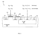
- FIG. 3 illustrates an exemplary cross section of a double-gate semiconductor device comprising a MOS gate and a junction gate and a single N+ region disposed between the MOS gate and the junction gate.
- Double-gate semiconductor device 300 may be formed from regions and/or layers of doped silicon, polysilicon, metal, and insulating layers using semiconductor fabrication techniques known in the art.
- Double-gate semiconductor device 300 comprises P- substrate 110, a N- well 120 formed in the P- substrate 110, N+ source 130, gate 140, oxide layer 150, N+ region 360, P+ gate 170, and N+ drain 180. As illustrated in FIG. 3 , N+ region 360 is disposed substantially in the N- well 120.
- electrical signals such as V g1 and control voltage V g2 may be coupled to gate 140 and P+ gate 170, respectively. Electrical signals may also be coupled to N+ source 130, N+ region 360 and N+ drain 180 using additional polysilicon layers (not shown) or metal layers (not shown) disposed on a surface of each of the N+ source 130, N+ region 360 and N+ drain 180 using semiconductor fabrication techniques known in the art.
- Double-gate semiconductor device 300 includes an N-type MOS gate formed by P- substrate 110, gate 140, and oxide layer 150.
- the double-gate semiconductor device 300 also includes an N-channel JFET formed by P- substrate 110, N- well 120, N+ region 360, P+ gate 170 and N+ drain 180.
- the N+ region 360 is a source of the N-channel JFET and abuts the N-type MOS gate, the N-type MOS gate comprising gate 140 and oxide layer 150.
- the double-gate semiconductor device 300 may be considered to operate analogously to the two modes as described herein with respect to FIGs. 1-2 .
- a first mode is indicated by V g1 > a threshold voltage V th and
- V g1 is applied to gate 140 that is greater than V th so that the MOS gate is "on.”
- a control voltage V g2 is applied to P+ gate 170 so that the junction gate is biased with a low potential difference between control voltage V g2 and a voltage V PI of the N+ region 360.
- the P+ gate 170 thus presents a low resistance, R on , to the current flow.
- the semiconductor device 300 conducts a current between N+ source 130 and N+ drain 180.
- the semiconductor device 300 does not conduct the current.
- the P+ gate 170 (the junction gate) may, therefore, be considered as behaving equivalently to a variable resistor with a high effective resistance, R off , that allows little or no current flow between N+ source 130 and N+ drain 180 when
- the double-gate-semiconductor device 300 may be considered to be a device with a double-gate in which the control voltage V g2 at P+ gate 170, the junction gate, may be a function of the voltage V g1 at gate 140.
- the MOS gate and the junction gate may both be dynamically biased in the "on" state or "off” state at the same time using a control circuitry described with reference to FIG. 5 .
- the control circuitry may comprise a capacitor (not shown) configured to couple a RF signal from gate 140 to P+ gate 170, as described with reference to FIG. 1 .
- the high effective resistance, R off allows the P+ gate 170 to sustain a high voltage and limits the voltage potential between gate 140 and N+ region 360 to less than the MOS gate breakdown voltage. Because the breakdown voltage of the double-gate semiconductor device 300 is the sum of the breakdown voltages of the MOS gate and the P+ gate 170, the intrinsically high breakdown voltage of the P+ gate 170 provides the high breakdown voltage of the double-gate semiconductor device 300.
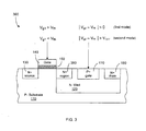
- FIG. 4 illustrates an exemplary cross section of the double-gate semiconductor device 300 of FIG. 3 in a second mode of operation.
- the description herein of the double gate semiconductor device 300 in a second mode of operation applies analogously to the second mode of operation of the double-gate semiconductor devices 100 and 200 described with reference to FIGs. 1-2 , respectively.
- the voltage V g1 applied to gate 140 is lower than the threshold voltage, V th , so that the MOS gate is "off."
- a control voltage V g2 is applied to the P+ gate 170 so that the junction gate is biased near the pinch-off voltage, V off, by using a high potential difference between V g2 and a voltage V PI of the N+ region 360.
- the P+ gate 170 thus presents a high effective resistance, R off , to the current flow in a drift region, such as drift region 420 illustrated in FIG. 4 .
- the high effective resistance, R off results from a depletion region extending under and around the P+ gate 170, such as depletion region 410 illustrated in FIG. 4 .
- the high effective resistance, R off in the second mode of operation allows the P+ gate 170 to sustain a high voltage and limits the voltage swing at gate 140 to less than the MOS gate breakdown voltage.
- the second mode of operation effectively protects the gate 140 from voltages greater than the breakdown voltage. Because the breakdown voltage of the double-gate semiconductor device 300 is the sum of the breakdown voltages of the MOS gate and the P+ gate 170, the intrinsically high breakdown voltage of the P+ gate 170 provides the high breakdown voltage of the double-gate semiconductor device 300.
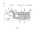
- FIG. 5 illustrates an exemplary circuit diagram of the double-gate semiconductor devices of FIGs. 1-2 .
- the circuit 500 comprises N-channel JFET 510, N-channel MOSFET 520, and control circuitry 530.
- the control circuitry 530 provides a control voltage V g2 to the gate of N-channel JFET 510 that may be a function of the voltage V g1 of the N-channel MOSFET 520.
- the control circuitry 530 functions to dynamically bias both the N-channel MOSFET 520 and N-channel JFET 510 in the "on" state or the "off” state at the same time.
- Control circuitry 530 may be a capacitor that may couple a RF signal from the gate of the N-channel MOSFET to the gate of the N-channel JFET.
- the control circuitry 530 provides the control voltage V g2 to bias N-channel JFET 510 so that the R off effective resistance is a maximum value when the N-channel MOSFET is "off" (i.e., V g1 ⁇ V th ).
- the control voltage V g2 biases N-channel JFET 510 close to the pinch-off voltage, V off .
- control circuitry 530 provides the control voltage V g2 to bias N-channel JFET 510 so that the R on effective resistance is minimal and the current flow is a maximum.
- the double-gate semiconductor devices described with reference to FIGs. 1-2 may also be represented by a circuit diagram similar to circuit 500 in which N-channel junction gate 510 may be substituted with a P-channel junction gate (not shown) and N-channel MOS gate 520 may be substituted with a P-channel MOS gate (not shown).
- FIG. 6 illustrates a cross section of a double-gate semiconductor device, according to an alternative embodiment of the invention.
- the double-gate semiconductor device 600 may be fabricated in a higher spatial density configuration than the embodiments described with reference to FIGs. 1-4 .
- double-gate semiconductor device 600 does not include a N+ region such as the N+ region 160, N+ region 162, N+ region 260, N+ region 262 and N+ region 360 described with reference to FIGs. 1-4 .
- the double-gate semiconductor device 600 is fabricated without the common implantation of an N+ region between the MOS gate and the junction gate.
- the principle of operation of the double-gate semiconductor device 600 is analogous to the principles of operation of the double-gate semiconductor devices 100, 200 and 300 described with reference to FIGs. 1-3 , including the description of the second mode of operation described with reference to FIG. 4 .
- Double-gate semiconductor device 600 may be formed from regions and/or layers of doped silicon, polysilicon, metal, and insulating layers using semiconductor fabrication techniques known in the art.
- the double-gate semiconductor device 600 comprises P- substrate 110, a N- well 120 formed in the P- substrate 110, N+ source 130, gate 140, oxide layer 150, P+ gate 170 and N+ drain 180.
- Electrical signals such as V g1 and control voltage V g2 , may be coupled to gate 140, and P+ gate 170, respectively. Electrical signals may be coupled to N+ source 130 and N+ drain 180 using additional polysilicon layers (not shown) or metal layers (not shown) disposed on a surface of each of the N+ source 130 and N+ drain 180 using semiconductor fabrication techniques known in the art.
- the double-gate semiconductor device 600 may be considered to operate analogously to the two modes of operation described with reference to FIGs. 1-4 .
- a current conducts between N+ source 130 and N+ drain 180.
- the current does not conduct.
- a voltage V g1 is applied to gate 140 that is greater than a threshold voltage V th (not shown).
- a control voltage V g2 is applied to the P+ gate 170, thus presenting a low effective resistance, R on , to the current flow.
- the voltage V g1 applied to gate 140 is lower than a threshold voltage, V th and a control voltage V g2 is applied P+ gate 170, thus presenting a high effective resistance, R off , to the current flow.
- the high effective resistance, R off results from a depletion region, similar to the depletion region 410 described with reference to FIG. 4 , that extends under and around P+ gate 170.
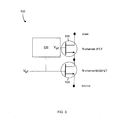
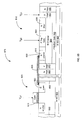
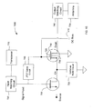
- FIG. 7 provides a circuit diagram for an exemplary electronic circuit 700 for amplifying an input signal such as an RF signal.
- the electronic circuit 700 comprises a MOSFET 705 and a dual-gate JFET 710 in a cascode configuration.
- the JFET 710 functions as a variable resistor.
- the MOSFET 705 and dual-gate JFET 710 are distinct transistors. As used herein, two transistors are defined as distinct unless the transistors share a common implantation region. As an example, N+ regions 260 and 262 ( FIG. 2 ) are drain and source, respectively, of distinct transistors. As another example, N+ regions 160 and 162 ( FIG. 1 ) are drain and source, respectively, of transistors that are not distinct since the two share a N+ implantation region.
- the MOSFET 705 includes a drain and a source, and in operation the source is coupled to a power supply such as V DD .
- the MOSFET 705 is controlled by a gate which, in operation, receives an input signal, for example an RF signal, from a signal source such as transceiver 715.
- Various embodiments of circuit 700 include an input matching circuit 720 between the transceiver 715 and the gate of the MOSFET 705 to match the impedances on either side thereof.
- An exemplary matching circuit 720 comprises a capacitor and an inductor where the capacitor is coupled between ground and a node between the transceiver 715 and the gate of the MOSFET 705, and the inductor is disposed in-line between the node and the gate of the MOSFET 705.
- the gate length of the MOSFET 705, i.e. the length of the gate implant located between the source and the drain, is less than one micron. It is noted that gate width is the dimension of the gate in the plane of the substrate measured perpendicular to the gate length.
- the MOSFET 705 can be a NMOSFET or a PMOSFET.
- the signal source such as transceiver 715, is disposed on the same substrate as the MOSFET 705 and the dual-gate JFET 710, in some embodiments.
- the signal source produces a signal with a frequency in the range of about 700MHz to about 2.5GHz.
- the signal source produces a signal with a frequency in the range of about 150MHz to about 6GHz.
- the dual-gate JFET 710 comprises a source and a drain electrically connected by a channel that is controlled by two gates, a top gate 725 and a bottom gate 730 disposed above and below the channel, respectively.
- the dual gate JFET 710 can be a NJFET or a PJFET.
- the dual-gate JFET 710 comprises a sub-micron gate length.
- the drain of the dual-gate JFET 710 is coupled to an antenna 735 or another device configured for signal transmission.
- the antenna 735 is coupled to the drain of the dual-gate JFET 710 by an output matching circuit 740 formed with passive networks, also provided to match impedances.
- the source of the dual-gate JFET 710 is coupled to the drain of the MOSFET 705. In some embodiments, the source of the dual-gate JFET 710 is directly coupled to the drain of the MOSFET 705. As used herein, “directly coupled” means that there are no active components in electrical communication between the coupled transistors. In some embodiments, the source of the dual-gate JFET 710 is coupled to the drain of the MOSFET 705 through vias and a trace such as conducting layer 265 ( FIG. 2 ). In some embodiments a point between the source of the dual-gate JFET 710 and the drain of the MOSFET 705 comprises a common node (CN) point. As shown in FIG. 7 , the electronic circuit 700 can also comprise, in some instances, an optional common node circuit 750 coupled between the common node point and ground.
- CN common node
- the JFET 710 is controlled by a top gate 725 and a bottom gate 730.
- the top and bottom gates 725, 730 are dependent (e.g. commonly controlled) or independent, and can be controlled by ground, a DC bias, the input signal applied to the gate of the MOSFET 705, or the input signal plus a DC bias.
- Various exemplary ways to control the top and bottom gates 725, 730 are discussed with reference to FIGs. 9-15 .
- the top and bottom gates 725, 730 are commonly controlled by the output of an optional JFET gates circuit 745 which is analogous to control circuit 530 ( FIG. 5 ).
- the JFET gates circuit 745 serves to improve the performance of embodiments of the invention that are used as a power amplifier.
- the bias of the bottom gate 730 determines the voltage of the top gate 725 to pinch off the JFET 710 where the pinch-off voltage of the JFET 710 is the limit value for the drain of the MOSFET 705.
- An appropriate value for the bottom gate 730 bias is one that allows that the pinch-off voltage of the JFET 710 to protect the MOSFET 705 in its reliable zone.
- the top gate 725 of the JFET 710 is maintained at 0V.
- the function of the JFET gate circuit 745 is to cancel these signals on the top gate 725 by applying an opposing signal.
- the electronic circuit 700 can also comprise, in some instances, an optional common node circuit 750 coupled between the common node point and ground.
- the common node circuit 750 also serves to improve the performance of embodiments of the invention that are used as a power amplifier.
- the common node circuit 750 compensates for the effect of the gate-to-drain capacitance of the MOSFET 705 and the gate-to-source capacitance of the JFET 710.
- the common node circuit 750 can be, in some embodiments, a single inductance or a serial inductor-capacitor (LC) network configured to resonate with the noted capacitances of the MOSFET 705 and the JFET 710 at the particular frequency.
- LC serial inductor-capacitor
- FIG. 8A provides a cross section of an exemplary electronic circuit 800 comprising a MOSFET 805 and a dual-gate JFET 810 where the MOSFET 805 and the JFET 810 comprise distinct transistors.
- the MOSFET 805 and the dual-gate JFET 810 can be formed from regions and/or layers of doped silicon, polysilicon, various metals, and various insulating layers using semiconductor fabrication techniques known in the art.
- a source 815 of the dual-gate JFET 810 is directly coupled to a drain 820 of the MOSFET 805 by a metal layer 825 and vias 830.
- the MOSFET 805 and a dual-gate JFET 810 can be implemented at different locations on the same substrate and with different dimensions, such as different widths.
- the JFET 810 additionally comprises a drain 835, a top gate 840, and a bottom gate 845.
- the top gate 840 and bottom gate 845 are disposed above and below an N channel 850 that couples the source 815 to the drain 820 of the JFET 810.
- the bottom gate 845 is bounded by two P wells 855 that provide an electrical connection to the bottom gate 845.
- the JFET 810 is disposed within an N well region that comprises two N wells 860 and an N isolation layer 865.
- the P wells 855 also serve to isolate the N channel 850 from the N wells 860 in these embodiments.
- a gate 870 of the MOSFET 805 is controlled by a signal V g1 .
- the top gate 840 and bottom gate 845 of the JFET 810 are controlled by signals V g2 and V g3 , respectively.
- the signal V g2 may be dependent upon, or independent of, the signal V g1 .
- the signal V g3 may be dependent upon, or independent of, the signal V g2 .
- FIG. 8B provides a cross section of another exemplary electronic circuit 877 comprising a MOSFET 805 and a dual-gate JFET 810 where the MOSFET 805 and the JFET 810 comprise distinct transistors.
- each of the MOSFET 805 and the dual-gate JFET 810 are disposed within separate N well regions.
- the N well region within which the MOSFET 805 is disposed is bounded by two N wells 880 and an N isolation layer 885.
- FIG. 9 provides a circuit diagram for an exemplary electronic circuit 900 that comprises the electronic circuit 700 and further comprises a DC bias source 910 coupled to the top and bottom gates 725, 730.
- a DC bias voltage is added to the input signal to control the top and bottom gates 725, 730.
- the DC bias voltage can be positive or negative, in various embodiments.
- a negative gate voltage can be applied on the top and bottom gates 725, 730 to decrease the common node voltage, ensuring in this way that the drain of the MOSFET 805 remains in its reliable zone.
- a positive voltage can be applied on the top and bottom gates 725, 730 to use the complete excursion of the reliable drain voltage to increase performance.
- the MOS and JFET gates circuit 745 and the common node circuit 750 are both optional.
- FIG. 10 provides a circuit diagram for an exemplary electronic circuit 1000 that comprises the electronic circuit 700 and further comprises a first DC bias source 1010 coupled to the top gate 725 and a second DC bias source 1020 coupled to the bottom gate 730.
- independent DC bias voltages are added to the input signal to independently control each of the top and bottom gates 725, 730.
- Each DC bias voltage can be positive or negative, in various embodiments.
- a capacitor 1030 is added between both top and bottom gates 725, 730 to allow a different DC bias to be applied to each, while applying the same RF coupling to each of the top and bottom gates 725, 730 as is applied to the gate of the MOSFET 705.
- FIG. 11 provides a circuit diagram for an exemplary electronic circuit 1100 that comprises the electronic circuit 700 but without the MOS and JFET gates circuit 745 and wherein the top gate 725 and the bottom gate 730 are both coupled to ground.
- FIG. 12 provides a circuit diagram for an exemplary electronic circuit 1200 that comprises the electronic circuit 700 but without the MOS and JFET gates circuit 745 and wherein the top gate 725 and the bottom gate 730 are both coupled to the DC bias source 910.
- the DC bias voltage can be positive or negative, in various embodiments.
- FIG. 13 provides a circuit diagram for an exemplary electronic circuit 1300 that comprises the electronic circuit 700 but without the MOS and JFET gates circuit 745. Additionally, as opposed to FIG. 7 , the first DC bias source 1010 is coupled to the top gate 725 and the second DC bias source 1020 is coupled to the bottom gate 730 rather than the top and bottom gates 725, 730 being dependent. Each DC bias voltage can be positive or negative, in various embodiments. In those embodiments illustrated by FIGs. 11-13 control of the top and bottom gates 725, 730 is independent of the input signal.
- FIG. 14 provides a circuit diagram for an exemplary electronic circuit 1400 that comprises the electronic circuit 1300 and further comprises the MOS and JFET gates circuit 745.
- FIG. 15 provides a circuit diagram for an exemplary electronic circuit 1500 that comprises the electronic circuit 700, modified such that the bottom gate 730 is independent of the top gate 725, and further comprising the DC bias source 910 coupled to the top gate 725 while the bottom gate 730 is coupled to ground. In those embodiments illustrated by FIGs. 14 and 15 control of the top gate 725 is dependent upon the input signal while control of the bottom gate 730 is independent of the input signal.
- An advantage to only applying the RF signal to the top gate 725 of the JFET 710 is that the capacitance between top gate 725 and drain or source terminals is smaller than the capacitances between the bottom gate 730 and the source or drain terminals, and that the top gate 725 is more efficient than the bottom gate 730 for controlling the channel current flow.
- FIG. 16 provides a flowchart representation of an exemplary method 1600 for amplifying a signal with a MOSFET 705 in a cascode configuration with a dual-gate JFET 710.
- the method comprises a step 1610 of controlling a gate of a MOSFET with a first signal, namely, the input signal to be amplified, a step 1620 of controlling a top gate of a JFET with a second signal, and a step 1630 of controlling a bottom gate of the JFET with a third signal. It will be appreciated that the steps illustrated by FIG. 16 are intended to be performed concurrently.
- the second signal is dependent upon the first signal and in some of these embodiments the two signals are the same, for example, where the gate of the MOSFET and the top gate of the JFET are capacitively coupled.
- the third signal is also dependent on the first and second signals, such as is illustrated by FIG. 7 , while in other embodiments the third signal is independent of the first and second signals, such as in FIGs. 14 and 15 .
- the second signal is independent of the first signal, such as is illustrated by FIGs. 11-13 .
- the third signal is dependent upon the second signal while in other embodiments the third signal is independent of the second signal.
- the first signal comprises the sum of the input signal and a DC bias.
- either or both of the second and third signals can be a fixed DC bias, either positive or negative, or ground.
Claims (15)
- Elektronische Schaltung, umfassend:einen MOSFET (705, 805), der eine Source (130), ein Drain (160, 260, 360, 820) und ein Gate (140, 870) aufweist; undeinen vom MOSFET gesonderten JFET (710, 810), der eine Source, ein Drain, ein oberes Gate (725, 840) und ein unteres Gate (730, 845) aufweist, wobei oberes und unteres Gate jeweils ober- und unterhalb eines Kanals des JFET angeordnet sind, wobei die Source des JFET unmittelbar an das Drain des MOSFET gekoppelt ist, dadurch gekennzeichnet, dass das obere Gate (725, 840) des JFET an das Gate des MOSFET gekoppelt ist.
- Elektronische Schaltung nach Anspruch 1, wobei sowohl das obere als auch das untere Gate (725, 730, 840, 845) des JFET an das Gate des MOSFET gekoppelt sind.
- Elektronische Schaltung nach einem der vorstehenden Ansprüche, wobei das obere und das untere Gate (725, 730, 840, 845) des JFET an eine DC-Biasquelle (910, 1010, 1020) gekoppelt sind.
- Elektronische Schaltung nach einem der vorstehenden Ansprüche, wobei das obere Gate des JFET über eine JFET-Gate-Schaltung (745) an das Gate des MOSFET gekoppelt ist.
- Elektronische Schaltung nach Anspruch 1, wobei das obere Gate (725, 840) des JFET an das Gate des MOSFET (705, 805) gekoppelt ist und das untere Gate (730, 845) des JFET unabhängig vom Gate des MOSFET ist.
- Elektronische Schaltung nach Anspruch 5, wobei das obere Gate (725, 840) des JFET an eine DC-Biasquelle (910, 1010) gekoppelt ist.
- Elektronische Schaltung nach Anspruch 5, wobei das untere Gate (730, 845) des JFET an eine DC-Biasquelle (910, 1020) oder die Erde gekoppelt ist.
- Elektronische Schaltung nach einem der vorstehenden Ansprüche, ferner umfassend eine zwischen der Erde und einem gemeinsamen Knoten zwischen dem Drain des MOSFET (705, 805) und der Source des JFET (710, 810) gekoppelte gemeinsame Knotenschaltung, wobei insbesondere das obere und untere Gate des JFET beide an die Erde gekoppelt sind.
- Elektronische Schaltung nach einem der vorstehenden Ansprüche, wobei die Gates des MOSFET (705, 805) und des JFET (710, 810) unterschiedliche Breiten aufweisen.
- Vorrichtung, umfassend:einen Sendeempfänger (715); undeine über eine Eingangsabgleichsschaltung (720) an den Sendeempfänger gekoppelte Endstufe, die eine elektronische Schaltung (100, 200, 300, 500, 600, 700, 800, 875, 900, 1000, 1100, 1200, 1300, 1400, 1500) nach einem der vorstehenden Ansprüche aufweist.
- Vorrichtung nach Anspruch 10, wobei der Sendeempfänger zur Erzeugung eines Signals mit einer Frequenz im Bereich von etwa 150 MHz bis etwa 6 GHz, insbesondere etwa 700 MHz bis etwa 2,5 GHz konfiguriert ist.
- Vorrichtung nach einem der Ansprüche 10 bis 11, wobei der Sendeempfänger (715) auf demselben Substrat wie der MOSFET (705, 805) und der JFET (710, 810) angeordnet ist.
- Vorrichtung nach einem der Ansprüche 10 bis 12, ferner umfassend eine an das Drain des JFET gekoppelte Ausgangsabgleichsschaltung.
- Verfahren, umfassend:Steuern (1610) eines Gate eines MOSFET mit einem ersten Signal;Steuern (1620) ein oberes Gate eines JFET mit einem zweiten Signal, wobei sich der JFET mit dem MOSFET in einer Kaskodenanordnung befindet undSteuern (1630) eines unteren Gates des JFET mit einem dritten Signal, wobei das obere und untere Gate jeweils ober- und unterhalb eines Kanals des JFET angeordnet sind, dadurch gekennzeichnet, dass das zweite Signal vom ersten Signal abhängig ist.
- Verfahren nach Anspruch 14, wobei das dritte Signal vom zweiten Signal abhängt.
Applications Claiming Priority (3)
| Application Number | Priority Date | Filing Date | Title |
|---|---|---|---|
| US17168909P | 2009-04-22 | 2009-04-22 | |
| US12/686,573 US7969243B2 (en) | 2009-04-22 | 2010-01-13 | Electronic circuits including a MOSFET and a dual-gate JFET |
| PCT/US2010/030770 WO2010123712A1 (en) | 2009-04-22 | 2010-04-12 | Electronic circuits including a mosfet and a dual-gate jfet |
Publications (3)
| Publication Number | Publication Date |
|---|---|
| EP2422447A1 EP2422447A1 (de) | 2012-02-29 |
| EP2422447A4 EP2422447A4 (de) | 2013-03-06 |
| EP2422447B1 true EP2422447B1 (de) | 2014-11-05 |
Family
ID=42991613
Family Applications (1)
| Application Number | Title | Priority Date | Filing Date |
|---|---|---|---|
| EP10767521.7A Active EP2422447B1 (de) | 2009-04-22 | 2010-04-12 | Elektronische schaltungen mit einem mosfet und einem dual-gate-jfet |
Country Status (7)
| Country | Link |
|---|---|
| US (3) | US7969243B2 (de) |
| EP (1) | EP2422447B1 (de) |
| JP (1) | JP5386034B2 (de) |
| KR (1) | KR101335202B1 (de) |
| CN (1) | CN102414984B (de) |
| TW (1) | TWI351100B (de) |
| WO (1) | WO2010123712A1 (de) |
Families Citing this family (38)
| Publication number | Priority date | Publication date | Assignee | Title |
|---|---|---|---|---|
| US8008731B2 (en) | 2005-10-12 | 2011-08-30 | Acco | IGFET device having a RF capability |
| WO2009082706A1 (en) | 2007-12-21 | 2009-07-02 | The Trustees Of Columbia University In The City Of New York | Active cmos sensor array for electrochemical biomolecular detection |
| US8928410B2 (en) | 2008-02-13 | 2015-01-06 | Acco Semiconductor, Inc. | Electronic circuits including a MOSFET and a dual-gate JFET |
| US7863645B2 (en) * | 2008-02-13 | 2011-01-04 | ACCO Semiconductor Inc. | High breakdown voltage double-gate semiconductor device |
| US9240402B2 (en) | 2008-02-13 | 2016-01-19 | Acco Semiconductor, Inc. | Electronic circuits including a MOSFET and a dual-gate JFET |
| US7969243B2 (en) * | 2009-04-22 | 2011-06-28 | Acco Semiconductor, Inc. | Electronic circuits including a MOSFET and a dual-gate JFET |
| US7952431B2 (en) * | 2009-08-28 | 2011-05-31 | Acco Semiconductor, Inc. | Linearization circuits and methods for power amplification |
| US8058674B2 (en) * | 2009-10-07 | 2011-11-15 | Moxtek, Inc. | Alternate 4-terminal JFET geometry to reduce gate to source capacitance |
| JP5012930B2 (ja) * | 2010-02-15 | 2012-08-29 | 株式会社デンソー | ハイブリッドパワーデバイス |
| US8532584B2 (en) | 2010-04-30 | 2013-09-10 | Acco Semiconductor, Inc. | RF switches |
| US8481380B2 (en) * | 2010-09-23 | 2013-07-09 | International Business Machines Corporation | Asymmetric wedge JFET, related method and design structure |
| CN102130053B (zh) * | 2010-12-03 | 2014-08-13 | 华东光电集成器件研究所 | 一种n沟道jfet集成放大器的制造方法 |
| US8797104B2 (en) * | 2012-04-13 | 2014-08-05 | Taiwan Semiconductor Manufacturing Co., Ltd. | Amplifier with floating well |
| US10269658B2 (en) | 2012-06-29 | 2019-04-23 | Taiwan Semiconductor Manufacturing Company, Ltd. | Integrated circuit devices with well regions and methods for forming the same |
| WO2014062936A1 (en) * | 2012-10-17 | 2014-04-24 | The Trustees Of Columbia University In The City Of New York | Cmos-integrated jfet for dense low-noise bioelectronic platforms |
| US9111765B2 (en) * | 2012-11-19 | 2015-08-18 | Taiwan Semiconductor Manufacturing Company Limited | Integrated circuit (IC) structure |
| US9780211B2 (en) | 2012-12-31 | 2017-10-03 | Taiwan Semiconductor Manufacturing Company, Ltd. | Power cell and power cell circuit for a power amplifier |
| US9490248B2 (en) * | 2012-12-31 | 2016-11-08 | Taiwan Semiconductor Manufacturing Company, Ltd. | Power cell, power cell circuit for a power amplifier and a method of making and using a power cell |
| US9882012B2 (en) | 2013-05-13 | 2018-01-30 | Taiwan Semiconductor Manufacturing Company, Ltd. | Junction gate field-effect transistor (JFET) having source/drain and gate isolation regions |
| US9287413B2 (en) | 2013-05-13 | 2016-03-15 | Taiwan Semiconductor Manufacturing Company, Ltd. | Junction gate field-effect transistor (JFET) and semiconductor device |
| US9318487B2 (en) * | 2013-07-09 | 2016-04-19 | Taiwan Semiconductor Manufacturing Co., Ltd. | High performance power cell for RF power amplifier |
| US9071203B2 (en) * | 2013-07-11 | 2015-06-30 | Taiwan Semiconductor Manufacturing Co., Ltd. | CMOS cascode power cells |
| JP6229369B2 (ja) * | 2013-08-21 | 2017-11-15 | 三菱電機株式会社 | 電力増幅器 |
| US9202934B2 (en) * | 2013-10-16 | 2015-12-01 | Analog Devices Global | Junction field effect transistor, and method of manufacture thereof |
| CN104766887B (zh) * | 2014-01-03 | 2019-05-17 | 艾壳 | 包括mosfet和双栅极jfet的电子电路 |
| US9543290B2 (en) * | 2014-01-23 | 2017-01-10 | International Business Machines Corporation | Normally-off junction field-effect transistors and application to complementary circuits |
| US9460926B2 (en) * | 2014-06-30 | 2016-10-04 | Alpha And Omega Semiconductor Incorporated | Forming JFET and LDMOS transistor in monolithic power integrated circuit using deep diffusion regions |
| CN104702226A (zh) * | 2015-03-31 | 2015-06-10 | 宜确半导体(苏州)有限公司 | 一种改进的共源共栅射频功率放大器 |
| KR102343894B1 (ko) | 2015-04-07 | 2021-12-27 | 삼성디스플레이 주식회사 | 표시 장치 |
| US9853103B2 (en) * | 2016-04-07 | 2017-12-26 | Cirrus Logic, Inc. | Pinched doped well for a junction field effect transistor (JFET) isolated from the substrate |
| US9853637B1 (en) * | 2016-06-24 | 2017-12-26 | Infineon Technologies Ag | Dual gate switch device |
| US10218350B2 (en) | 2016-07-20 | 2019-02-26 | Semiconductor Components Industries, Llc | Circuit with transistors having coupled gates |
| US9947654B2 (en) | 2016-09-08 | 2018-04-17 | Semiconductor Components Industries, Llc | Electronic device including a transistor and a field electrode |
| TWI615966B (zh) * | 2016-12-29 | 2018-02-21 | 新唐科技股份有限公司 | 半導體元件 |
| US9941356B1 (en) * | 2017-04-20 | 2018-04-10 | Vanguard International Semiconductor Corporation | JFET and method for fabricating the same |
| US20190131404A1 (en) * | 2017-10-30 | 2019-05-02 | Analog Devices Global Unlimited Company | Low gate current junction field effect transistor device architecture |
| US10826485B2 (en) | 2018-12-17 | 2020-11-03 | Analog Devices International Unlimited Company | Cascode compound switch slew rate control |
| US11271108B2 (en) | 2020-04-08 | 2022-03-08 | International Business Machines Corporation | Low-noise gate-all-around junction field effect transistor |
Citations (1)
| Publication number | Priority date | Publication date | Assignee | Title |
|---|---|---|---|---|
| JPH10107214A (ja) * | 1996-10-01 | 1998-04-24 | Masashi Mukogawa | 半導体装置 |
Family Cites Families (78)
| Publication number | Priority date | Publication date | Assignee | Title |
|---|---|---|---|---|
| US567927A (en) * | 1896-09-15 | Machine | ||
| IT1094069B (it) | 1978-04-18 | 1985-07-26 | Muriotto Angelo | Procedimento per la produzione di pannelli prefabbricati ed elementi tridimensionali e prodotti ottenuti con tale procedimento |
| US4228367A (en) * | 1978-08-07 | 1980-10-14 | Precision Monolithics, Inc. | High speed integrated switching circuit for analog signals |
| US4255714A (en) * | 1979-02-21 | 1981-03-10 | Rca Corporation | GaAs Dual-gate FET frequency discriminator |
| US4353036A (en) | 1980-08-29 | 1982-10-05 | Rca Corporation | Field effect transistor amplifier with variable gain control |
| US4523111A (en) * | 1983-03-07 | 1985-06-11 | General Electric Company | Normally-off, gate-controlled electrical circuit with low on-resistance |
| US4811075A (en) * | 1987-04-24 | 1989-03-07 | Power Integrations, Inc. | High voltage MOS transistors |
| US4864454A (en) * | 1988-04-21 | 1989-09-05 | Analog Devices, Incorporated | Means for reducing damage to JFETs from electrostatic discharge events |
| JPH0399466A (ja) * | 1989-09-12 | 1991-04-24 | Fujitsu Ltd | 半導体装置およびその製造方法 |
| US5061903A (en) * | 1990-02-27 | 1991-10-29 | Grumman Aerospace Corporation | High voltage modified cascode circuit |
| KR950006483B1 (ko) * | 1990-06-13 | 1995-06-15 | 가부시끼가이샤 도시바 | 종형 mos트랜지스터와 그 제조방법 |
| KR960006004A (ko) * | 1994-07-25 | 1996-02-23 | 김주용 | 반도체 소자 및 그 제조방법 |
| US5677927A (en) | 1994-09-20 | 1997-10-14 | Pulson Communications Corporation | Ultrawide-band communication system and method |
| US5537078A (en) * | 1995-03-31 | 1996-07-16 | Linear Technology Corporation | Operational amplifier with JFET inputs having low input bias current and methods for using same |
| US5543643A (en) * | 1995-07-13 | 1996-08-06 | Lsi Logic Corporation | Combined JFET and MOS transistor device, circuit |
| US5684080A (en) | 1995-11-15 | 1997-11-04 | Shell Oil Company | Aqueous polymer emulsion |
| US6088484A (en) * | 1996-11-08 | 2000-07-11 | Hughes Electronics Corporation | Downloading of personalization layers for symbolically compressed objects |
| US6091295A (en) * | 1997-06-27 | 2000-07-18 | The Whitaker Corporation | Predistortion to improve linearity of an amplifier |
| US5969582A (en) * | 1997-07-03 | 1999-10-19 | Ericsson Inc. | Impedance matching circuit for power amplifier |
| US5912490A (en) * | 1997-08-04 | 1999-06-15 | Spectrian | MOSFET having buried shield plate for reduced gate/drain capacitance |
| US5898198A (en) * | 1997-08-04 | 1999-04-27 | Spectrian | RF power device having voltage controlled linearity |
| US6061008A (en) * | 1997-12-19 | 2000-05-09 | Rockwell Science Center, Inc. | Sigma-delta-sigma modulator for high performance analog-to-digital and digital-to-analog conversion |
| GB2336485B (en) | 1998-04-14 | 2002-12-11 | Roke Manor Research | Monopulse generator |
| US5918137A (en) | 1998-04-27 | 1999-06-29 | Spectrian, Inc. | MOS transistor with shield coplanar with gate electrode |
| KR100296146B1 (ko) * | 1998-05-23 | 2001-08-07 | 오길록 | 소신호선형화장치 |
| IL125022A (en) | 1998-06-21 | 2001-09-13 | Israel Bar David | Methods and apparatus for adaptive adjustment of feed-forward linearized amplifiers |
| US6384688B1 (en) * | 1998-07-08 | 2002-05-07 | Hitachi, Ltd. | High-frequency power amplifier module |
| US6312997B1 (en) | 1998-08-12 | 2001-11-06 | Micron Technology, Inc. | Low voltage high performance semiconductor devices and methods |
| US6061555A (en) * | 1998-10-21 | 2000-05-09 | Parkervision, Inc. | Method and system for ensuring reception of a communications signal |
| DE19902520B4 (de) * | 1999-01-22 | 2005-10-06 | Siemens Ag | Hybrid-Leistungs-MOSFET |
| DE19902519C2 (de) * | 1999-01-22 | 2002-04-18 | Siemens Ag | Hybrid-Leistungs-MOSFET für hohe Stromtragfähigkeit |
| TW443039B (en) * | 1999-05-20 | 2001-06-23 | Ind Tech Res Inst | Sigma-delta modulator by using method of local nonlinear feedback loop |
| DE19926715C1 (de) * | 1999-06-11 | 2001-01-18 | Siemens Ag | Verfahren und Vorrichtung zum Abschalten einer Kaskodenschaltung mit spannungsgesteuerten Halbleiterschaltern |
| US6242978B1 (en) | 1999-06-30 | 2001-06-05 | Harris Corporation | Method and apparatus for linearizing an amplifier |
| US6584205B1 (en) * | 1999-08-26 | 2003-06-24 | American Technology Corporation | Modulator processing for a parametric speaker system |
| DE69938363T2 (de) | 1999-11-29 | 2008-06-26 | Multispectral Solutions, Inc. | Ultrabreitband-datenvermittlungssystem |
| US6300835B1 (en) * | 1999-12-10 | 2001-10-09 | Motorola, Inc. | Power amplifier core |
| CA2294404C (en) * | 2000-01-07 | 2004-11-02 | Tadeuse A. Kwasniewski | Delta-sigma modulator for fractional-n frequency synthesis |
| JP4018312B2 (ja) * | 2000-02-21 | 2007-12-05 | 株式会社ルネサステクノロジ | 無線通信装置 |
| EP1319252B1 (de) * | 2000-09-21 | 2012-02-15 | Cambridge Semiconductor Limited | Halbleiterbauelement und dessen herstellungsverfahren |
| WO2002056477A2 (en) * | 2001-01-12 | 2002-07-18 | Broadcom Corp | Gain scaling for higher signal-to-noise ratios in multistage, multi-bit delta sigma modulators |
| US6735419B2 (en) | 2001-01-18 | 2004-05-11 | Motorola, Inc. | High efficiency wideband linear wireless power amplifier |
| KR100487813B1 (ko) * | 2001-01-19 | 2005-05-10 | 인티그런트 테크놀로지즈(주) | 상보 소자를 이용한 싱글엔드형 차동 회로 |
| KR100489693B1 (ko) * | 2001-02-16 | 2005-05-17 | 인티그런트 테크놀로지즈(주) | 선형성이 향상된 증폭 회로 및 믹서 회로 |
| US6503782B2 (en) * | 2001-03-02 | 2003-01-07 | Mississippi State University Research And Technology Corporation (Rtc) | Complementary accumulation-mode JFET integrated circuit topology using wide (>2eV) bandgap semiconductors |
| US6600369B2 (en) | 2001-12-07 | 2003-07-29 | Motorola, Inc. | Wideband linear amplifier with predistortion error correction |
| US20030227320A1 (en) * | 2002-06-05 | 2003-12-11 | Intel Corporation | Buffer, buffer operation and method of manufacture |
| US7209715B2 (en) | 2002-07-30 | 2007-04-24 | Matsushita Electric Industrial Co., Ltd. | Power amplifying method, power amplifier, and communication apparatus |
| KR20040104177A (ko) * | 2003-06-03 | 2004-12-10 | 삼성전기주식회사 | 시분할방식 전력증폭모듈 |
| JP4262545B2 (ja) * | 2003-07-09 | 2009-05-13 | 三菱電機株式会社 | カスコード接続回路及びその集積回路 |
| US7049669B2 (en) * | 2003-09-15 | 2006-05-23 | Infineon Technologies Ag | LDMOS transistor |
| JP4868433B2 (ja) * | 2004-02-09 | 2012-02-01 | ソニー・エリクソン・モバイルコミュニケーションズ株式会社 | 歪み補償装置および歪み補償機能付き電力増幅装置 |
| TWI224869B (en) * | 2004-03-25 | 2004-12-01 | Richtek Techohnology Corp | Apparatus for driving depletion type junction field effect transistor |
| WO2005099098A1 (en) * | 2004-04-09 | 2005-10-20 | Audioasics A/S | Sigma delta modulator |
| JP2006013753A (ja) * | 2004-06-24 | 2006-01-12 | Renesas Technology Corp | 無線通信システムおよび半導体集積回路 |
| US7312481B2 (en) * | 2004-10-01 | 2007-12-25 | Texas Instruments Incorporated | Reliable high-voltage junction field effect transistor and method of manufacture therefor |
| US20080291973A1 (en) | 2004-11-16 | 2008-11-27 | Acco | Integrated Ultra-Wideband (Uwb) Pulse Generator |
| US7348826B1 (en) | 2005-03-18 | 2008-03-25 | Qspeed Semiconductor Inc. | Composite field effect transistor |
| US20060228850A1 (en) * | 2005-04-06 | 2006-10-12 | Pang-Yen Tsai | Pattern loading effect reduction for selective epitaxial growth |
| US7253758B2 (en) * | 2005-07-20 | 2007-08-07 | Industrial Technology Research Institute | Third order sigma-delta modulator |
| JP4821214B2 (ja) | 2005-08-26 | 2011-11-24 | 三菱電機株式会社 | カスコード接続回路 |
| US8008731B2 (en) | 2005-10-12 | 2011-08-30 | Acco | IGFET device having a RF capability |
| RU2316334C2 (ru) | 2005-12-19 | 2008-02-10 | Медитек Индастриз ЛЛС | Способ активации утраченных двигательных функций, а также определения эффективности их восстановления при повреждении центральной нервной системы |
| US7411231B2 (en) * | 2005-12-22 | 2008-08-12 | Analog Devices, Inc. | JFET with drain and/or source modification implant |
| US7634240B2 (en) | 2006-01-31 | 2009-12-15 | Motorola, Inc. | Method and apparatus for controlling a supply voltage to a power amplifier |
| KR20070079724A (ko) * | 2006-02-03 | 2007-08-08 | 고상원 | 전력 증폭기의 선형화를 위한 전치 보정회로 |
| US7554397B2 (en) * | 2006-05-22 | 2009-06-30 | Theta Microelectronics, Inc. | Highly linear low-noise amplifiers |
| US7894772B2 (en) * | 2006-08-04 | 2011-02-22 | Axiom Microdevices, Inc. | Low distortion radio frequency (RF) limiter |
| DE102006045312B3 (de) * | 2006-09-26 | 2008-05-21 | Siced Electronics Development Gmbh & Co. Kg | Halbleiteranordnung mit gekoppelten Sperrschicht-Feldeffekttransistoren |
| US7636056B2 (en) * | 2007-05-22 | 2009-12-22 | Panasonic Corporation | Delta sigma modulator operating with different power source voltages |
| US7679448B1 (en) * | 2007-08-30 | 2010-03-16 | Pmc-Sierra, Inc. | Continuous wave based bias method and apparatus for minimizing MOS transistor distortion |
| US7522079B1 (en) * | 2007-09-06 | 2009-04-21 | National Semiconductor Corporation | Sigma-delta modulator with DAC resolution less than ADC resolution and increased tolerance of non-ideal integrators |
| US7656229B2 (en) * | 2008-01-28 | 2010-02-02 | Qualcomm, Incorporated | Method and apparatus for reducing intermodulation distortion in an electronic device having an amplifier circuit |
| US7969243B2 (en) * | 2009-04-22 | 2011-06-28 | Acco Semiconductor, Inc. | Electronic circuits including a MOSFET and a dual-gate JFET |
| US7863645B2 (en) * | 2008-02-13 | 2011-01-04 | ACCO Semiconductor Inc. | High breakdown voltage double-gate semiconductor device |
| US8170505B2 (en) * | 2008-07-30 | 2012-05-01 | Qualcomm Incorporated | Driver amplifier having a programmable output impedance adjustment circuit |
| US7808415B1 (en) | 2009-03-25 | 2010-10-05 | Acco Semiconductor, Inc. | Sigma-delta modulator including truncation and applications thereof |
| US7952431B2 (en) | 2009-08-28 | 2011-05-31 | Acco Semiconductor, Inc. | Linearization circuits and methods for power amplification |
-
2010
- 2010-01-13 US US12/686,573 patent/US7969243B2/en active Active
- 2010-04-12 JP JP2012507253A patent/JP5386034B2/ja active Active
- 2010-04-12 EP EP10767521.7A patent/EP2422447B1/de active Active
- 2010-04-12 KR KR1020117027746A patent/KR101335202B1/ko active IP Right Grant
- 2010-04-12 WO PCT/US2010/030770 patent/WO2010123712A1/en active Application Filing
- 2010-04-12 CN CN201080017947.3A patent/CN102414984B/zh active Active
- 2010-04-22 TW TW099112711A patent/TWI351100B/zh active
-
2011
- 2011-05-13 US US13/107,411 patent/US8179197B2/en active Active
-
2012
- 2012-04-10 US US13/443,611 patent/US8400222B2/en active Active
Patent Citations (1)
| Publication number | Priority date | Publication date | Assignee | Title |
|---|---|---|---|---|
| JPH10107214A (ja) * | 1996-10-01 | 1998-04-24 | Masashi Mukogawa | 半導体装置 |
Also Published As
| Publication number | Publication date |
|---|---|
| JP2012525003A (ja) | 2012-10-18 |
| EP2422447A4 (de) | 2013-03-06 |
| JP5386034B2 (ja) | 2014-01-15 |
| US8179197B2 (en) | 2012-05-15 |
| US20100271133A1 (en) | 2010-10-28 |
| US20120205724A1 (en) | 2012-08-16 |
| US7969243B2 (en) | 2011-06-28 |
| CN102414984B (zh) | 2015-12-16 |
| CN102414984A (zh) | 2012-04-11 |
| KR20120030379A (ko) | 2012-03-28 |
| US8400222B2 (en) | 2013-03-19 |
| KR101335202B1 (ko) | 2013-11-29 |
| US20110215871A1 (en) | 2011-09-08 |
| TW201044558A (en) | 2010-12-16 |
| WO2010123712A1 (en) | 2010-10-28 |
| EP2422447A1 (de) | 2012-02-29 |
| TWI351100B (en) | 2011-10-21 |
Similar Documents
| Publication | Publication Date | Title |
|---|---|---|
| EP2422447B1 (de) | Elektronische schaltungen mit einem mosfet und einem dual-gate-jfet | |
| US9627374B2 (en) | Electronic circuits including a MOSFET and a dual-gate JFET | |
| US20200321467A1 (en) | Method and apparatus for use in improving linearity of mosfets using an accumulated charge sink-harmonic wrinkle reduction | |
| US7863645B2 (en) | High breakdown voltage double-gate semiconductor device | |
| US8928410B2 (en) | Electronic circuits including a MOSFET and a dual-gate JFET | |
| US7696572B2 (en) | Split source RF MOSFET device | |
| US10181478B2 (en) | Radio frequency switch having field effect transistor cells | |
| EP2248181B1 (de) | Doppelgate-halbleiteranordnung mit hoher durchschlagspannung | |
| CN104766887B (zh) | 包括mosfet和双栅极jfet的电子电路 | |
| EP2892079B1 (de) | Elektronische Schaltungen mit einem MOSFET und einem Dual-Gate-JFET | |
| CN107769742B (zh) | 具有放大器-mosfet的集成电路 | |
| CN102983169B (zh) | 高击穿电压的双栅极半导体器件 |
Legal Events
| Date | Code | Title | Description |
|---|---|---|---|
| PUAI | Public reference made under article 153(3) epc to a published international application that has entered the european phase |
Free format text: ORIGINAL CODE: 0009012 |
|
| 17P | Request for examination filed |
Effective date: 20111116 |
|
| AK | Designated contracting states |
Kind code of ref document: A1 Designated state(s): AT BE BG CH CY CZ DE DK EE ES FI FR GB GR HR HU IE IS IT LI LT LU LV MC MK MT NL NO PL PT RO SE SI SK SM TR |
|
| RIN1 | Information on inventor provided before grant (corrected) |
Inventor name: MASLIAH, DENIS Inventor name: BRACALE, ALEXANDRE |
|
| DAX | Request for extension of the european patent (deleted) | ||
| A4 | Supplementary search report drawn up and despatched |
Effective date: 20130206 |
|
| RIC1 | Information provided on ipc code assigned before grant |
Ipc: H03F 1/22 20060101ALI20130131BHEP Ipc: H03F 3/14 20060101AFI20130131BHEP Ipc: H01L 27/06 20060101ALI20130131BHEP Ipc: H03F 3/24 20060101ALI20130131BHEP Ipc: H03F 3/195 20060101ALI20130131BHEP |
|
| 17Q | First examination report despatched |
Effective date: 20131127 |
|
| GRAP | Despatch of communication of intention to grant a patent |
Free format text: ORIGINAL CODE: EPIDOSNIGR1 |
|
| INTG | Intention to grant announced |
Effective date: 20140731 |
|
| GRAS | Grant fee paid |
Free format text: ORIGINAL CODE: EPIDOSNIGR3 |
|
| GRAA | (expected) grant |
Free format text: ORIGINAL CODE: 0009210 |
|
| RIN1 | Information on inventor provided before grant (corrected) |
Inventor name: MASLIAH, DENIS Inventor name: BRACALE, ALEXANDRE |
|
| AK | Designated contracting states |
Kind code of ref document: B1 Designated state(s): AT BE BG CH CY CZ DE DK EE ES FI FR GB GR HR HU IE IS IT LI LT LU LV MC MK MT NL NO PL PT RO SE SI SK SM TR |
|
| REG | Reference to a national code |
Ref country code: GB Ref legal event code: FG4D |
|
| REG | Reference to a national code |
Ref country code: CH Ref legal event code: EP |
|
| REG | Reference to a national code |
Ref country code: AT Ref legal event code: REF Ref document number: 695052 Country of ref document: AT Kind code of ref document: T Effective date: 20141115 |
|
| REG | Reference to a national code |
Ref country code: IE Ref legal event code: FG4D |
|
| REG | Reference to a national code |
Ref country code: DE Ref legal event code: R096 Ref document number: 602010020001 Country of ref document: DE Effective date: 20141224 |
|
| REG | Reference to a national code |
Ref country code: FR Ref legal event code: PLFP Year of fee payment: 6 |
|
| REG | Reference to a national code |
Ref country code: AT Ref legal event code: MK05 Ref document number: 695052 Country of ref document: AT Kind code of ref document: T Effective date: 20141105 |
|
| REG | Reference to a national code |
Ref country code: NL Ref legal event code: VDEP Effective date: 20141105 |
|
| REG | Reference to a national code |
Ref country code: LT Ref legal event code: MG4D |
|
| PG25 | Lapsed in a contracting state [announced via postgrant information from national office to epo] |
Ref country code: PT Free format text: LAPSE BECAUSE OF FAILURE TO SUBMIT A TRANSLATION OF THE DESCRIPTION OR TO PAY THE FEE WITHIN THE PRESCRIBED TIME-LIMIT Effective date: 20150305 Ref country code: FI Free format text: LAPSE BECAUSE OF FAILURE TO SUBMIT A TRANSLATION OF THE DESCRIPTION OR TO PAY THE FEE WITHIN THE PRESCRIBED TIME-LIMIT Effective date: 20141105 Ref country code: IS Free format text: LAPSE BECAUSE OF FAILURE TO SUBMIT A TRANSLATION OF THE DESCRIPTION OR TO PAY THE FEE WITHIN THE PRESCRIBED TIME-LIMIT Effective date: 20150305 Ref country code: NL Free format text: LAPSE BECAUSE OF FAILURE TO SUBMIT A TRANSLATION OF THE DESCRIPTION OR TO PAY THE FEE WITHIN THE PRESCRIBED TIME-LIMIT Effective date: 20141105 Ref country code: NO Free format text: LAPSE BECAUSE OF FAILURE TO SUBMIT A TRANSLATION OF THE DESCRIPTION OR TO PAY THE FEE WITHIN THE PRESCRIBED TIME-LIMIT Effective date: 20150205 Ref country code: ES Free format text: LAPSE BECAUSE OF FAILURE TO SUBMIT A TRANSLATION OF THE DESCRIPTION OR TO PAY THE FEE WITHIN THE PRESCRIBED TIME-LIMIT Effective date: 20141105 Ref country code: LT Free format text: LAPSE BECAUSE OF FAILURE TO SUBMIT A TRANSLATION OF THE DESCRIPTION OR TO PAY THE FEE WITHIN THE PRESCRIBED TIME-LIMIT Effective date: 20141105 |
|
| PG25 | Lapsed in a contracting state [announced via postgrant information from national office to epo] |
Ref country code: LV Free format text: LAPSE BECAUSE OF FAILURE TO SUBMIT A TRANSLATION OF THE DESCRIPTION OR TO PAY THE FEE WITHIN THE PRESCRIBED TIME-LIMIT Effective date: 20141105 Ref country code: AT Free format text: LAPSE BECAUSE OF FAILURE TO SUBMIT A TRANSLATION OF THE DESCRIPTION OR TO PAY THE FEE WITHIN THE PRESCRIBED TIME-LIMIT Effective date: 20141105 Ref country code: GR Free format text: LAPSE BECAUSE OF FAILURE TO SUBMIT A TRANSLATION OF THE DESCRIPTION OR TO PAY THE FEE WITHIN THE PRESCRIBED TIME-LIMIT Effective date: 20150206 Ref country code: CY Free format text: LAPSE BECAUSE OF FAILURE TO SUBMIT A TRANSLATION OF THE DESCRIPTION OR TO PAY THE FEE WITHIN THE PRESCRIBED TIME-LIMIT Effective date: 20141105 Ref country code: SE Free format text: LAPSE BECAUSE OF FAILURE TO SUBMIT A TRANSLATION OF THE DESCRIPTION OR TO PAY THE FEE WITHIN THE PRESCRIBED TIME-LIMIT Effective date: 20141105 Ref country code: PL Free format text: LAPSE BECAUSE OF FAILURE TO SUBMIT A TRANSLATION OF THE DESCRIPTION OR TO PAY THE FEE WITHIN THE PRESCRIBED TIME-LIMIT Effective date: 20141105 Ref country code: HR Free format text: LAPSE BECAUSE OF FAILURE TO SUBMIT A TRANSLATION OF THE DESCRIPTION OR TO PAY THE FEE WITHIN THE PRESCRIBED TIME-LIMIT Effective date: 20141105 |
|
| PG25 | Lapsed in a contracting state [announced via postgrant information from national office to epo] |
Ref country code: CZ Free format text: LAPSE BECAUSE OF FAILURE TO SUBMIT A TRANSLATION OF THE DESCRIPTION OR TO PAY THE FEE WITHIN THE PRESCRIBED TIME-LIMIT Effective date: 20141105 Ref country code: SK Free format text: LAPSE BECAUSE OF FAILURE TO SUBMIT A TRANSLATION OF THE DESCRIPTION OR TO PAY THE FEE WITHIN THE PRESCRIBED TIME-LIMIT Effective date: 20141105 Ref country code: EE Free format text: LAPSE BECAUSE OF FAILURE TO SUBMIT A TRANSLATION OF THE DESCRIPTION OR TO PAY THE FEE WITHIN THE PRESCRIBED TIME-LIMIT Effective date: 20141105 Ref country code: DK Free format text: LAPSE BECAUSE OF FAILURE TO SUBMIT A TRANSLATION OF THE DESCRIPTION OR TO PAY THE FEE WITHIN THE PRESCRIBED TIME-LIMIT Effective date: 20141105 |
|
| REG | Reference to a national code |
Ref country code: DE Ref legal event code: R097 Ref document number: 602010020001 Country of ref document: DE |
|
| PLBE | No opposition filed within time limit |
Free format text: ORIGINAL CODE: 0009261 |
|
| STAA | Information on the status of an ep patent application or granted ep patent |
Free format text: STATUS: NO OPPOSITION FILED WITHIN TIME LIMIT |
|
| REG | Reference to a national code |
Ref country code: GB Ref legal event code: S117 Free format text: REQUEST FILED; REQUEST FOR CORRECTION UNDER SECTION 117 FILED ON 17 DECEMBER 2014 |
|
| 26N | No opposition filed |
Effective date: 20150806 |
|
| REG | Reference to a national code |
Ref country code: GB Ref legal event code: S117 Free format text: CORRECTIONS ALLOWED; REQUEST FOR CORRECTION UNDER SECTION 117 FILED ON 17 DECEMBER 2014, ALLOWED ON 15 SEPTEMBER 2015 |
|
| PG25 | Lapsed in a contracting state [announced via postgrant information from national office to epo] |
Ref country code: MC Free format text: LAPSE BECAUSE OF FAILURE TO SUBMIT A TRANSLATION OF THE DESCRIPTION OR TO PAY THE FEE WITHIN THE PRESCRIBED TIME-LIMIT Effective date: 20141105 Ref country code: LU Free format text: LAPSE BECAUSE OF FAILURE TO SUBMIT A TRANSLATION OF THE DESCRIPTION OR TO PAY THE FEE WITHIN THE PRESCRIBED TIME-LIMIT Effective date: 20150412 |
|
| REG | Reference to a national code |
Ref country code: CH Ref legal event code: PL |
|
| PG25 | Lapsed in a contracting state [announced via postgrant information from national office to epo] |
Ref country code: IT Free format text: LAPSE BECAUSE OF FAILURE TO SUBMIT A TRANSLATION OF THE DESCRIPTION OR TO PAY THE FEE WITHIN THE PRESCRIBED TIME-LIMIT Effective date: 20141105 |
|
| REG | Reference to a national code |
Ref country code: IE Ref legal event code: MM4A |
|
| PG25 | Lapsed in a contracting state [announced via postgrant information from national office to epo] |
Ref country code: LI Free format text: LAPSE BECAUSE OF NON-PAYMENT OF DUE FEES Effective date: 20150430 Ref country code: CH Free format text: LAPSE BECAUSE OF NON-PAYMENT OF DUE FEES Effective date: 20150430 |
|
| REG | Reference to a national code |
Ref country code: FR Ref legal event code: PLFP Year of fee payment: 7 |
|
| PG25 | Lapsed in a contracting state [announced via postgrant information from national office to epo] |
Ref country code: SI Free format text: LAPSE BECAUSE OF FAILURE TO SUBMIT A TRANSLATION OF THE DESCRIPTION OR TO PAY THE FEE WITHIN THE PRESCRIBED TIME-LIMIT Effective date: 20141105 |
|
| REG | Reference to a national code |
Ref country code: FR Ref legal event code: RM Effective date: 20160205 |
|
| PG25 | Lapsed in a contracting state [announced via postgrant information from national office to epo] |
Ref country code: IE Free format text: LAPSE BECAUSE OF NON-PAYMENT OF DUE FEES Effective date: 20150412 |
|
| REG | Reference to a national code |
Ref country code: DE Ref legal event code: R081 Ref document number: 602010020001 Country of ref document: DE Owner name: SOMOS SEMICONDUCTOR, FR Free format text: FORMER OWNER: ACCO SEMICONDUCTOR, INC., SUNNYVALE, CALIF., US Ref country code: DE Ref legal event code: R082 Ref document number: 602010020001 Country of ref document: DE Representative=s name: LAVOIX MUNICH, DE Ref country code: DE Ref legal event code: R081 Ref document number: 602010020001 Country of ref document: DE Owner name: ACCO, FR Free format text: FORMER OWNER: ACCO SEMICONDUCTOR, INC., SUNNYVALE, CALIF., US |
|
| PG25 | Lapsed in a contracting state [announced via postgrant information from national office to epo] |
Ref country code: RO Free format text: LAPSE BECAUSE OF FAILURE TO SUBMIT A TRANSLATION OF THE DESCRIPTION OR TO PAY THE FEE WITHIN THE PRESCRIBED TIME-LIMIT Effective date: 20141105 |
|
| REG | Reference to a national code |
Ref country code: FR Ref legal event code: TP Owner name: ACCO, FR Effective date: 20160622 |
|
| PG25 | Lapsed in a contracting state [announced via postgrant information from national office to epo] |
Ref country code: MT Free format text: LAPSE BECAUSE OF FAILURE TO SUBMIT A TRANSLATION OF THE DESCRIPTION OR TO PAY THE FEE WITHIN THE PRESCRIBED TIME-LIMIT Effective date: 20141105 |
|
| REG | Reference to a national code |
Ref country code: FR Ref legal event code: PLFP Year of fee payment: 8 |
|
| PG25 | Lapsed in a contracting state [announced via postgrant information from national office to epo] |
Ref country code: BG Free format text: LAPSE BECAUSE OF FAILURE TO SUBMIT A TRANSLATION OF THE DESCRIPTION OR TO PAY THE FEE WITHIN THE PRESCRIBED TIME-LIMIT Effective date: 20141105 Ref country code: SM Free format text: LAPSE BECAUSE OF FAILURE TO SUBMIT A TRANSLATION OF THE DESCRIPTION OR TO PAY THE FEE WITHIN THE PRESCRIBED TIME-LIMIT Effective date: 20141105 Ref country code: HU Free format text: LAPSE BECAUSE OF FAILURE TO SUBMIT A TRANSLATION OF THE DESCRIPTION OR TO PAY THE FEE WITHIN THE PRESCRIBED TIME-LIMIT; INVALID AB INITIO Effective date: 20100412 |
|
| PG25 | Lapsed in a contracting state [announced via postgrant information from national office to epo] |
Ref country code: TR Free format text: LAPSE BECAUSE OF FAILURE TO SUBMIT A TRANSLATION OF THE DESCRIPTION OR TO PAY THE FEE WITHIN THE PRESCRIBED TIME-LIMIT Effective date: 20141105 |
|
| PG25 | Lapsed in a contracting state [announced via postgrant information from national office to epo] |
Ref country code: BE Free format text: LAPSE BECAUSE OF FAILURE TO SUBMIT A TRANSLATION OF THE DESCRIPTION OR TO PAY THE FEE WITHIN THE PRESCRIBED TIME-LIMIT Effective date: 20141105 |
|
| REG | Reference to a national code |
Ref country code: FR Ref legal event code: PLFP Year of fee payment: 9 |
|
| PG25 | Lapsed in a contracting state [announced via postgrant information from national office to epo] |
Ref country code: MK Free format text: LAPSE BECAUSE OF FAILURE TO SUBMIT A TRANSLATION OF THE DESCRIPTION OR TO PAY THE FEE WITHIN THE PRESCRIBED TIME-LIMIT Effective date: 20141105 |
|
| REG | Reference to a national code |
Ref country code: DE Ref legal event code: R082 Ref document number: 602010020001 Country of ref document: DE Representative=s name: LAVOIX MUNICH, DE Ref country code: DE Ref legal event code: R081 Ref document number: 602010020001 Country of ref document: DE Owner name: SOMOS SEMICONDUCTOR, FR Free format text: FORMER OWNER: ACCO, LOUVECIENNES, FR |
|
| PGFP | Annual fee paid to national office [announced via postgrant information from national office to epo] |
Ref country code: FR Payment date: 20230321 Year of fee payment: 14 |
|
| PGFP | Annual fee paid to national office [announced via postgrant information from national office to epo] |
Ref country code: DE Payment date: 20230321 Year of fee payment: 14 |
|
| PGFP | Annual fee paid to national office [announced via postgrant information from national office to epo] |
Ref country code: GB Payment date: 20240321 Year of fee payment: 15 |