EP2416352A2 - Verfahren zur Herstellung von Grabenmetalloxid-Halbleiter-Feldeffekttransistoren - Google Patents
Verfahren zur Herstellung von Grabenmetalloxid-Halbleiter-Feldeffekttransistoren Download PDFInfo
- Publication number
- EP2416352A2 EP2416352A2 EP11172625A EP11172625A EP2416352A2 EP 2416352 A2 EP2416352 A2 EP 2416352A2 EP 11172625 A EP11172625 A EP 11172625A EP 11172625 A EP11172625 A EP 11172625A EP 2416352 A2 EP2416352 A2 EP 2416352A2
- Authority
- EP
- European Patent Office
- Prior art keywords
- layers
- layer
- epi
- oxide
- trench
- Prior art date
- Legal status (The legal status is an assumption and is not a legal conclusion. Google has not performed a legal analysis and makes no representation as to the accuracy of the status listed.)
- Withdrawn
Links
Images


Classifications
-
- H—ELECTRICITY
- H10—SEMICONDUCTOR DEVICES; ELECTRIC SOLID-STATE DEVICES NOT OTHERWISE PROVIDED FOR
- H10D—INORGANIC ELECTRIC SEMICONDUCTOR DEVICES
- H10D30/00—Field-effect transistors [FET]
- H10D30/01—Manufacture or treatment
- H10D30/021—Manufacture or treatment of FETs having insulated gates [IGFET]
- H10D30/028—Manufacture or treatment of FETs having insulated gates [IGFET] of double-diffused metal oxide semiconductor [DMOS] FETs
- H10D30/0291—Manufacture or treatment of FETs having insulated gates [IGFET] of double-diffused metal oxide semiconductor [DMOS] FETs of vertical DMOS [VDMOS] FETs
- H10D30/0297—Manufacture or treatment of FETs having insulated gates [IGFET] of double-diffused metal oxide semiconductor [DMOS] FETs of vertical DMOS [VDMOS] FETs using recessing of the gate electrodes, e.g. to form trench gate electrodes
-
- H—ELECTRICITY
- H01—ELECTRIC ELEMENTS
- H01L—SEMICONDUCTOR DEVICES NOT COVERED BY CLASS H10
- H01L21/00—Processes or apparatus adapted for the manufacture or treatment of semiconductor or solid state devices or of parts thereof
- H01L21/02—Manufacture or treatment of semiconductor devices or of parts thereof
- H01L21/02104—Forming layers
- H01L21/02365—Forming inorganic semiconducting materials on a substrate
- H01L21/02612—Formation types
- H01L21/02617—Deposition types
- H01L21/02636—Selective deposition, e.g. simultaneous growth of mono- and non-monocrystalline semiconductor materials
- H01L21/02639—Preparation of substrate for selective deposition
-
- H—ELECTRICITY
- H01—ELECTRIC ELEMENTS
- H01L—SEMICONDUCTOR DEVICES NOT COVERED BY CLASS H10
- H01L21/00—Processes or apparatus adapted for the manufacture or treatment of semiconductor or solid state devices or of parts thereof
- H01L21/02—Manufacture or treatment of semiconductor devices or of parts thereof
- H01L21/02104—Forming layers
- H01L21/02365—Forming inorganic semiconducting materials on a substrate
- H01L21/02612—Formation types
- H01L21/02617—Deposition types
- H01L21/02636—Selective deposition, e.g. simultaneous growth of mono- and non-monocrystalline semiconductor materials
- H01L21/02647—Lateral overgrowth
-
- H—ELECTRICITY
- H10—SEMICONDUCTOR DEVICES; ELECTRIC SOLID-STATE DEVICES NOT OTHERWISE PROVIDED FOR
- H10D—INORGANIC ELECTRIC SEMICONDUCTOR DEVICES
- H10D30/00—Field-effect transistors [FET]
- H10D30/60—Insulated-gate field-effect transistors [IGFET]
- H10D30/64—Double-diffused metal-oxide semiconductor [DMOS] FETs
- H10D30/66—Vertical DMOS [VDMOS] FETs
- H10D30/668—Vertical DMOS [VDMOS] FETs having trench gate electrodes, e.g. UMOS transistors
-
- H—ELECTRICITY
- H10—SEMICONDUCTOR DEVICES; ELECTRIC SOLID-STATE DEVICES NOT OTHERWISE PROVIDED FOR
- H10D—INORGANIC ELECTRIC SEMICONDUCTOR DEVICES
- H10D62/00—Semiconductor bodies, or regions thereof, of devices having potential barriers
- H10D62/10—Shapes, relative sizes or dispositions of the regions of the semiconductor bodies; Shapes of the semiconductor bodies
- H10D62/13—Semiconductor regions connected to electrodes carrying current to be rectified, amplified or switched, e.g. source or drain regions
- H10D62/149—Source or drain regions of field-effect devices
- H10D62/151—Source or drain regions of field-effect devices of IGFETs
- H10D62/156—Drain regions of DMOS transistors
- H10D62/157—Impurity concentrations or distributions
-
- H—ELECTRICITY
- H10—SEMICONDUCTOR DEVICES; ELECTRIC SOLID-STATE DEVICES NOT OTHERWISE PROVIDED FOR
- H10D—INORGANIC ELECTRIC SEMICONDUCTOR DEVICES
- H10D64/00—Electrodes of devices having potential barriers
- H10D64/20—Electrodes characterised by their shapes, relative sizes or dispositions
- H10D64/27—Electrodes not carrying the current to be rectified, amplified, oscillated or switched, e.g. gates
- H10D64/311—Gate electrodes for field-effect devices
- H10D64/411—Gate electrodes for field-effect devices for FETs
- H10D64/511—Gate electrodes for field-effect devices for FETs for IGFETs
- H10D64/514—Gate electrodes for field-effect devices for FETs for IGFETs characterised by the insulating layers
- H10D64/516—Gate electrodes for field-effect devices for FETs for IGFETs characterised by the insulating layers the thicknesses being non-uniform
-
- H10P14/271—
-
- H10P14/276—
Definitions
- MOSFETs power metal oxide semiconductor field effect transistors
- Planar MOSFETs became available in the mid-1970s.
- trench MOSFETs started penetrating power MOSFET markets utilizing dynamic random access memory (DRAM) trench technology, which has improved the specific on-resistance between drain and source (RDSON).
- DRAM dynamic random access memory
- the trench MOSFET has a major advantage over the planar MOSFET in terms of current densities due to the benefits of a vertical channel for better cell pitch.
- the trench MOSFET suffers from high gate drain charges Q GD .
- the high Q GD can limit the power supply ability of the trench MOSFET.
- MOSFET W-gated trench MOSFET
- a trench bottom oxide (TBO) structure can be achieved by conventional local oxidation of silicon (LOCOS) technology to reduce the Q GD of the WMOSFET.
- LOCOS local oxidation of silicon
- the stress ofTBO in the WMOSFET created from the LOCOS technology including the known bird's beak effect, introduces a long-term reliability problem.
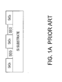
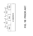
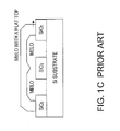
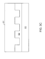
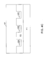
- FIGs. 1A-1C illustrate cross-sectional views of structure diagrams of epitaxial (epi) options over patterned oxide atop substrates for conventional MOSFETs.
- SEG selective epitaxial growth
- ELO epitaxial lateral overgrowth
- MELO merged epitaxial lateral overgrowth
- a trench metal oxide semiconductor field effect transistor is fabricated in an upward direction.
- a trench bottom doping (TBD) process and/or a trench bottom oxide (TBO) process are performed after formation of a substrate and a first epitaxial (epi) layer.
- Poly seal is performed after the formation of TBO layers and before a merged epitaxial lateral overgrowth (MELO) step to improve quality and purity of a second epi layer formed in the MELO step.
- Plasma dry etching with an end point mode is performed according to the locations of TBO layers to improve the uniformity of trench depth.
- FIGs. 1A-1C illustrate cross-sectional views of structure diagrams of epitaxial options over patterned oxide atop substrates for conventional metal oxide semiconductor field effect transistors (MOSFETs).
- MOSFETs metal oxide semiconductor field effect transistors
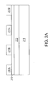
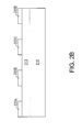
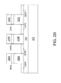
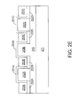
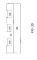
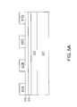
- FIGs. 2 ,A-2F illustrate cross-sectional views of a fabrication sequence of a trench MOSFET, in accordance with one embodiment of the present invention.
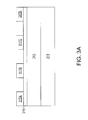
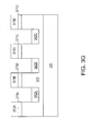
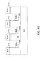
- FIGs. 3A-3I illustrate cross-sectional views of a fabrication sequence of a trench MOSFET, in accordance with another embodiment of the present invention.
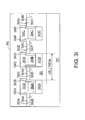
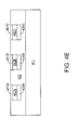
- FIGs. 4A-4I illustrate cross-sectional views of a fabrication sequence of a trench MOSFET, in accordance with yet another embodiment of the present invention.
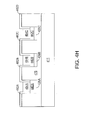
- FIGs. 5A-5F illustrate cross-sectional views of a fabrication sequence of a trench MOSFET, in accordance with yet another embodiment of the present invention.
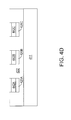
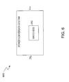
- FIG. 6 illustrates a block diagram of a power conversion system, in accordance with one embodiment of the invention.
- Embodiments according to the present invention provide methods for fabricating a trench metal oxide semiconductor field effect transistor (MOSFET) in an upward direction relative to the substrate.
- the upward technology makes parameters of each layer easier to control without extra fabrication steps.
- a trench bottom doping (TBD) process and/or a trench bottom oxide (TBO) process are performed on a partial thickness of an epitaxial (epi) layer atop a substrate.
- a merged epitaxial lateral overgrowth (MELO) step is performed to grow the rest of the epi thickness.
- FIGs. 2A-2F illustrate cross-sectional views of a fabrication sequence of a trench metal oxide semiconductor field effect transistor (MOSFET), in accordance with one embodiment of the present invention.
- MOSFET trench metal oxide semiconductor field effect transistor
- epitaxial (epi) deposition is performed to form an epi layer on the top of a semiconductor substrate 211 of a wafer.
- the thickness of the epi layer is approximately two (2) ⁇ m.
- the semiconductor substrate 211 as a bottom layer can constitute a drain region of the trench MOSFET.
- a partial thickness of the epi layer is oxidized to produce a predetermined TBO thickness, e.g., 1000-5000A.
- a first photoresist is deposited to form photoresist regions 217A-217D.
- the photoresist regions 217A-217D act as soft masks to pattern trench areas for the trench MOSFET, e.g., the locations for the trenches of the trench MOSFET.
- oxide windows e.g., part of the oxide layer 215
- oxide layers 222A-222D are etched away to form oxide layers 222A-222D, and then the first photoresist is removed. Consequently, a trench bottom oxide (TBO) process is performed in FIG. 2A and FIG. 2B .
- TBO trench bottom oxide
- a merged epitaxial lateral overgrowth (MELO) step is performed to grow the rest of the epi thickness of the trench MOSFET.
- MELO merged epitaxial lateral overgrowth
- an epi layer 231 is formed to surround the oxide layers 222A-222D as Si seeds.
- the epi thickness is grown to thicker than five (5) ⁇ m until the total epi thickness can grow to about seven (7) ⁇ m to meet a thickness that can sustain a breakdown voltage (BV) of the trench MOSFET.
- BV breakdown voltage
- hard mask oxidation is performed on the top of the epi layer 213 to form an oxide layer which is grown to about 200-1000A.
- a second photoresist is deposited to pattern the oxide layer, and photoresist regions 246A-246C are formed atop the oxide layer and pattern the locations for the trenches of the trench MOSFET.
- the edges of the photoresist regions 246A-246C are aligned to the edges of the oxide layers 222A-222D.
- Plasma dry etching with an end point mode is performed to remove the silicon and the oxide from part of the epi layer 231 and from part of the oxide layer to form epi layers 242A-242C and oxide layers 244A-244C.
- end points for the trench etching are preset according to the locations of TBO layers, e.g., the oxide layers 222A-222C.
- an intelligent sensor (not shown) detects that the etching location reaches the end points, the plasma dry etching is stopped.
- the trenches of the trench MOSFET are formed.
- variations in the uniformity of trench depth across the wafer will be significantly reduced to less than ( ⁇ ) 1 % compared with variations of greater than (>) 10% experienced with a conventional timed trench etching mode.
- a sacrificial oxide layer is grown thermally on the top of the oxide layers 222A-222D and 244A-244C. Then the sacrificial oxide layer and the oxide layers 244A-244C are stripped away by wet buffered oxide etching (BOE) to remove surface defects and smooth surface roughness.
- BOE wet buffered oxide etching
- Gate oxidation is performed surrounding the epi layers 242A-242C to form gate oxide layers 251A-251C with a predetermined thickness.
- poly film is deposited with doping in-situ or ex-situ to form polysilicon layers. The polysilicon layers are etched back with an end point mode. Hence, slight poly recess etching is performed to form polysilicon layers 253A-253D. As a result, the trenches are filled with the polysilicon layers 253A-253D with a predetermined thickness.
- P-type dopants or N-type dopants for the channel body are implanted and driven in the epi-layers 242A-242C to form P-wells or N-wells 261A-261C.
- the P-wells or N-wells 261A-261C can form body regions of the trenches.
- N-type dopants are implanted and driven in to form N-type heavily doped (N+) layers 262A-262F.
- Borophosphorosilicate glass (BPSG) is deposited to form BPSG layers 263A-263D atop the gate oxide layers 260A-260F.
- an implantation of P-type dopants followed by a drive-in step, an etching step, and an anneal step is performed to form P-type heavily doped (P+) layers 264A-264C adjacent to the N+ layers 262A-262F.
- the N+ layers 262A-262F can form source regions of the trench MOSFET.
- Metallization is performed to separate gate and source metal connections.
- the entire trench MOSFET can be metalized by a metal layer 265.
- passivation is performed to isolate the trench MOSFET from the external environment.
- the fabrication processes of the trench MOSFET are performed upward, and hence it is easier to control the implant profile, shape, and thickness of each layer of the trench MOSFET.
- repetitive processes to achieve the predetermined profile, shape, and thickness of each layer can be avoided, and the simpler processes can reduce the cost of fabricating the trench MOSFET.
- the quality and purity of each layer can be also improved.
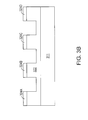
- FIGs. 3A-3I illustrate cross-sectional views of a fabrication sequence of a trench MOSFET, in accordance with another embodiment of the present invention.
- epitaxial (epi) deposition is performed to form an epi layer on the top of a semiconductor substrate 311 of a wafer.
- the semiconductor substrate 311 as a bottom layer can constitute a drain region of the trench MOSFET.
- a partial thickness of the epi layer is oxidized, e.g., the oxide thickness can be 200-1000A.
- an oxide layer 315 is formed atop an epi layer 313.
- a first photoresist is deposited to form photoresist regions 317A-317D.
- the photoresist regions 317A-317D act as soft masks to pattern trench areas for the trench MOSFET, e.g., the locations for the trenches of the trench MOSFET.
- oxide windows e.g., part of the oxide layers 315
- silicon trenches e.g., part of the epi layer 313
- oxide layers 324A-324D are etched away to form oxide layers 324A-324D and an epi layer 322. Then the first photoresist is removed.
- CVD chemical vapor deposition
- TEOS tetraethylorthosilicate
- the oxide layer 331 is etched back with an end point mode. Hence, trench recess etching is performed to form oxide layers 342A-342C. Consequently, a trench bottom oxide (TBO) process is performed in FIG. 3C-FIG. 3D .
- TBO trench bottom oxide
- poly film is deposited and etched back to form polysilicon layers 351A-351C in the trench areas of the trench MOSFET.
- a MELO step is performed to achieve the rest of the epi thickness of the trench MOSFET.
- the predetermined epi thickness for the trench MOSFET is easier to achieve to sustain a BV of the trench MOSFET.
- An epi layer 362 is formed atop the polysilicon layers 351A-351C.
- the polysilicon layers 351A-351C act as caps atop the oxide layers 342A-342C to seal out oxygen gas in the MELO step, which will reduce the number of oxygen atoms incorporated into the Si epi process and improve the quality of the epi layer 362.
- hard mask oxidation is performed on the top of the epi layer 362 to form an oxide layer which is grown to about 200-1000A as a hard mask oxide.
- a second photoresist is deposited to pattern the oxide layer, and photoresist regions 373A-373D are formed atop the oxide layer and pattern the locations for the trenches of the trench MOSFET.
- the edges of the photoresist regions 373A-373D are aligned to the edges of the oxide layers 342A-342D.
- Plasma dry etching with an end point mode is performed to remove the hard mask oxide and the silicon from part of the oxide layer and from part of the epi layer 362 to construct stacks of an epi layer 375 and oxide layers 371A-371D.
- the polysilicon layers 351A-351C are etched away.
- the trenches for the trench MOSFET are formed.
- variations in the uniformity of trench depth across the wafer can be reduced to, e.g., less than 1%.
- a sacrificial oxide layer is grown thermally on the top of the oxide layers 342A-342C and 371A-371D. Then the sacrificial oxide layer and the oxide layers 371A-371D are stripped away by wet buffered oxide etching (BOE) to remove surface defects and smooth surface roughness. Gate oxidation is performed surrounding the epi layer 375 to form gate oxide layers 382A-382D with a predetermined thickness. Then, poly film is deposited with doping in-situ or ex-situ to form polysilicon layers. The polysilicon layers are etched back with an end point mode. Hence, slightly poly recess etching is performed to form polysilicon layers 384A-384C. As a result, the trenches are filled with the polysilicon layers 384A-384C with a predetermined thickness.
- BOE wet buffered oxide etching
- P-type dopants or N-type dopants for the channel body are implanted and driven in the epi-layer 375 to form a P-well or N-well 391.
- the P-well or N-well 391 can form a body region of the trenches.
- N-type dopants are implanted and driven in to form N+ layers 392A-392H.
- BPSG is deposited to form BPSG layers 393A-393C atop gate oxide layers 390A-390F.
- an implantation of P-type dopants followed by a drive-in step, an etching step, and an anneal step is performed to form P+ layers 394A-394D adjacent to the N+ layers 392A-392H.
- the N+ layers 392A-392H can form source regions of the trench MOSFET.
- Metallization is performed to separate gate and source metal connections.
- the entire trench MOSFET can be metalized by a metal layer 395.
- passivation is performed to isolate the trench MOSFET from the external environment.
- the upward fabrication processes of the trench MOSFET make the parameters, e.g., the implant profile, shape and thickness, of each layer easier to control. Hence, extra fabrication steps are avoided, the cost of fabricating the trench MOSFET is reduced, and the quality and purity of each layer are improved.
- FIGs. 4A-4I illustrate cross-sectional views of a fabrication sequence of a trench MOSFET, in accordance with yet another embodiment of the present invention.
- epitaxial (epi) deposition is performed to form an epi layer on the top of a semiconductor substrate 411 of a wafer.
- the semiconductor substrate 411 as a bottom layer can constitute a drain region of the trench MOSFET.
- Partial thickness of the epi layer is oxidized, e.g., the oxide thickness can be 200-1000A.
- an oxide layer 415 is formed atop an epi layer 413.
- a first photoresist is deposited to form photoresist regions 417A-417D.
- the photoresist regions 417A-417D act as soft masks to pattern trench areas for the trench MOSFET, e.g., the locations for the trenches of the trench MOSFET.
- oxide windows e.g., part of the oxide layers 415
- silicon trenches e.g., part of the epi layer 413
- oxide layers 424A-424D and an epi layer 422.
- the first photoresist is removed.
- N+ doping materials e.g., polysilicon or spin-on phosphorus glass
- TCD trench bottom doping
- CVD chemical vapor deposition
- TEOS tetraethylorthosilicate
- the oxide layer 431 is etched back with an end point mode. Hence, trench recess etching is performed to form oxide layers 442A-442C. Consequently, a trench bottom oxide (TBO) process is performed in FIG. 4C-FIG. 4D .
- TBO trench bottom oxide
- poly film is deposited and etched back to form polysilicon layers 451A-451C in the trench areas of the trench MOSFET.
- a MELO step is performed to achieve the rest of the epi thickness of the trench MOSFET.
- the predetermined epi thickness for the trench MOSFET is easier to achieve to sustain a BV of the trench MOSFET.
- An epi layer 462 is formed atop the polysilicon layers 451A-451C.
- the polysilicon layers 451A-451C act as caps atop the oxide layers 442-442C to seal out oxygen gas in the MELO step.
- the quality of the epi layer 462 is improved.
- hard mask oxidation is performed on the top of the epi layer 462 to form an oxide layer which is grown to about 200-1000A as hard mask oxide.
- a second photoresist is deposited to pattern the oxide layer, and photoresist regions 473A-473D are formed atop the oxide layer and pattern the locations for the trenches of the trench MOSFET.
- the edges of the photoresist regions 473A-473D are aligned to the edges of the oxide layers 442A-442D.
- Plasma dry etching with an end point mode is performed to remove the hard mask oxide and the silicon from part of the oxide layer and from part of the epi layer 462 to construct stacks of an epi layer 475 and oxide layers 471A-471D.
- the polysilicon layers 451A-451C are etched away. Hence, the trenches for the trench MOSFET are formed.
- a sacrificial oxide layer is grown thermally on the top of the oxide layers 442A-442C and 471A-471D. Then, the sacrificial oxide layer and the oxide layers 471A-471D are stripped away by wet buffered oxide etching (BOE) to remove surface defects and smooth surface roughness. Gate oxidation is performed surrounding the epi layer 475 to form gate oxide layers 482A-482D with a predetermined thickness. Then, poly film is deposited with doping in-situ or ex-situ to form polysilicon layers. The polysilicon layers are etched back with an end point mode. Hence, slight poly recess etching is performed to form polysilicon layers 484A-484C. As a result, the trenches are filled with the polysilicon layers 484A-484C with a predetermined thickness.
- BOE wet buffered oxide etching
- P-type dopants or N-type dopants for the channel body are implanted and driven in the epi-layer 475 to form a P-well or N-well 491.
- the P-well or N-well 491 can form a body region of the trenches.
- N-type dopants are implanted and driven in to form N+ layers 492A-492H.
- BPSG is deposited to form BPSG layers 493A-493C atop gate oxide layers 490A-490F.
- an implantation of P-type dopants followed by a drive-in step, an etching step, and an anneal step is performed to form P+ layers 494A-494D adjacent to the N+ layers 492A-492H.
- the N+ layers 492A-492H can form source regions of the trench MOSFET.
- Metallization is performed to separate gate and source metal connections.
- the entire trench MOSFET can be metalized by a metal layer 495.
- passivation is performed to isolate the trench MOSFET from the external environment.
- the parameters, e.g., the implant profile, shape and thickness, of each layer are easier to control during the upward fabrication processes of the trench MOSFET.
- the uniformity of trench depth etched by dry plasma with end point mode is improved because the TBO process is performed in the middle of the epi steps and before the trench etching step. Hence, extra fabrication steps are avoided, the cost of fabricating the trench MOSFET is reduced, and the quality and purity of each layer are improved.
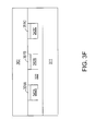
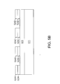
- FIGs. 5A-5F illustrate cross-sectional views of a fabrication sequence of a trench MOSFET, in accordance with yet another embodiment of the present invention.
- epitaxial (epi) deposition is performed to form an epi layer 513 on the top of a semiconductor substrate 511 of a wafer.
- the semiconductor substrate 511 as a bottom layer can constitute a drain region of the trench MOSFET.
- the N-type heavily epi deposition or implantation is performed to form an N+ epi layer atop the epi layer 513.
- a partial thickness of the N+ epi layer is oxidized for a predetermined TBO thickness, e.g., 200-1000A.
- an oxide layer 515 is formed atop an N+ epi layer 514.
- a first photoresist is deposited to form photoresist regions 517A-517D.
- the photoresist regions 517A-517D act as soft masks to pattern trench areas for the trench MOSFET, e.g., the locations for the trenches of the trench MOSFET.
- oxide windows e.g., part of the oxide layers 515
- silicon trenches e.g., part of the N+ epi layer 514
- oxide layers 524A-524D and N+ epi layers 522A-522D are etched away.
- the first photoresist is stripped away. Consequently, a TBD process and TBO process are performed in FIG. 5A-FIG. 5B .
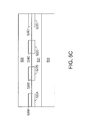
- a MELO step is performed to achieve the rest of the epi thickness of the trench MOSFET.
- the predetermined epi thickness for the trench MOSFET is easier to achieve to sustain a BV of the trench MOSFET.
- Epi layers 531 and 533 are formed to surround the N+ epi layers 522A-522D and the oxide layers 524A-524D.
- hard mask oxidation is performed on the top of the epi layer 533 to form an oxide layer which is grown to about 200-1000A as hard mask oxide.
- a second photoresist is deposited to pattern the oxide layer, and photoresist regions 546A-546C are formed atop the oxide layer and pattern the locations for the trenches of the trench MOSFET.
- the edges of the photoresist regions 546A-546C are aligned to the edges of the oxide layers 524A-524D.
- Plasma dry etching with an end point mode is performed to remove the hard mask oxide and the silicon from part of the oxide layer and from part of the epi layer 533 to construct stacks of epi layers 542A-542C and oxide layers 544A-544C. Hence, the trenches for the trench MOSFET are formed.
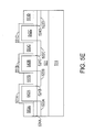
- a sacrificial oxide layer is grown thermally on the top of the oxide layers 524A-524D and 544A-544C. Then the sacrificial oxide layer and the oxide layers 544A-544C are stripped away by wet buffered oxide etching (BOE) to remove surface defects and smooth surface roughness.
- BOE wet buffered oxide etching
- Gate oxidation is performed surrounding the epi layers 542A-542C to form gate oxide layers 551A-551C with a predetermined thickness.
- poly film is deposited with doping in-situ or ex-situ to form polysilicon layers. The polysilicon layers are etched back with an end point mode. Hence, slightlypoly recess etching is performed to form polysilicon layers 553A-553D. As a result, the trenches are filled with polysilicon layers 553A-553D with a predetermined thickness.
- P-type dopants or N-type dopants for the channel body are implanted and driven in the epi layers 542A-542C to form P-wells or N-wells 561A-561C.
- the P-wells or N-wells 561A-561C can form body regions of the trenches.
- N-type heavily dopants are implanted and driven in to form N+ layers 562A-562F.
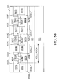
- BPSG is deposited to form BPSG layers 563A-563D atop gate oxide layers 560A-560F.
- an implantation of P-type dopants followed by a drive-in step, an etching step, and an anneal step is performed to form P+ layers 564A-564C adjacent to the N+ layers 562A-562F.
- the N+ layers 562A-562F can form source regions of the trench MOSFET.
- Metallization is performed to separate gate and source metal connections.
- the entire trench MOSFET can be metalized by a metal layer 565.
- passivation is performed to isolate the trench MOSFET from the external environment.
- the upward fabrication processes of the trench MOSFET make the parameters of each layer easier to control.
- the uniformity of trench depth etched by dry plasma with end point mode is improved because the TBO process is performed in the middle of the epi steps and before the trench etching step.
- extra fabrication steps are avoided, the cost of fabricating the trench MOSFET is reduced, and the quality and purity of each layer are improved.
- FIG. 6 illustrates a diagram of a power conversion system 600, in accordance with one embodiment of the invention.
- the power conversion system 600 can converter an input voltage to an output voltage.
- the power conversion system 600 can be a DC-DC converter, an AC-DC converter, or a DC-AC converter.
- the power conversion system 600 can include one or more switches 610.
- the switch 610 can be, but is not limited to, a trench MOSFET fabricated by the fabrication processes shown in FIGs. 2A-2F , FIGs. 3A-3I , FIGs. 4A-4I or FIG. 5A-5F .
- the switch 610 can be used as a high-side power switch or a low-side power switch in the power conversion system 600. Due to the improved uniformity and Si epi purity, and the reduced fabrication processes of the trench MOSFET, the switch 610 has relatively higher quality and lower cost. Switches fabricated by the above-mentioned processes will be in great demand for products such as notepads and smartphones for battery power management, DC-DC conversion, and so on.
- a trench bottom doping (TBD) process and/or a trench bottom oxide (TBO) process are performed after formation of a substrate 211, 311, 411 or 511 and an epi layer 213, 313, 413 or 513.
- the substrate 211, 311, 411 or 511 constitutes a drain region of the trench MOSFET.
- a first photoresist is deposited and photoresist regions 217A-217D, 317A-317D, 417A-417D or 517A-517D are formed to act as soft masks to pattern the trench areas of the trench MOSFET.
- N+ dopants are deposited into the trenches to form TBD layers, e.g., the N+ layers 426A-426C.
- Chemical vapor deposition (CVD) oxide or tetraethylorthosilicate (TEOS) is deposited and etched back to form the oxide layers 442A-442C atop the N+ layer 426A-426C.
- N+ dopants are implanted to form the N+ epi layer, and a partial thickness of the N+ epi layer is oxidized to form the oxide layer 515 atop the N+ layer 514.
- the N+ epi layer 514 and the oxide layer 515 are etched to form TBD layers, e.g., the N+ epi layers 522A-522D, and the oxide layers 524A-524D.
- a partial thickness of the epi layer is oxidized to form an oxide layer 215 atop the epi layer 213, and the oxide layer 215 is etched to form oxide layers 222A-222D.
- a partial thickness of the epi layer is oxidized to form the oxide layer 315 atop the epi layer 313, and etching of the oxide layer 315 is performed.
- CVD oxide or TEOS is deposited and etched back to form the oxide layers 342A-342C.
- the TBO thickness can be increased without stress compared to that fabricated by the conventional LOCOS technology.
- TBO layers e.g., the oxide layers 222A-222D, 342A-342D, 442A-442C or 524A-524D can grow to greater than 5000A, while the TBO thickness is less than 3000A in the conventional LOCOS application.
- a merged epitaxial lateral overgrowth (MELO) step is performed to grow the rest of the epi thickness of the trench MOSFET.
- MELO merged epitaxial lateral overgrowth
- BV breakdown voltage
- a poly seal step in FIG. 3E or in FIG. 4E is performed before the MELO step in FIG. 3F or FIG. 4F to improve the epi quality.
- Trench etching is performed by plasma dry etching with an end point mode. More specifically, end points for plasma dry etching are preset according to the location of the TBO layers, e.g., the oxide layers 222A-222D, 342A-342C, 442A-442C or 524A-524D.
- the plasma dry etching is stopped when the etching location reaches the location of the TBO layers.
- the trench depth uniformity is improved by using the end point mode. Hence, silicon at the locations of the trenches is etched away and the trenches of the trench MOSFET are formed.
- a sacrificial oxidation is grown thermally, and sacrificial etching is performed to remove surface defects and smooth surface roughness.
- the oxide layers fabricated by the TBO process have better purity and better quality.
- gate oxidization is performed.
- the thickness of the gate oxide in the lower part of the trenches is greater than 3000A, and the thickness of the gate oxide in the upper part of the trenches is between about 200A and 1000A.
- poly film is deposited and etched back to achieve slight poly recession.
- P-wells or N-wells for channel body are formed and constitute body regions of the trenches.
- N+ layers are formed and constitute source regions of the trench MOSFET.
- Borophosphosilicate glass (BPSG) layers are formed atop the gate oxide layers.
- P+ layers are formed adjacent to the N+ layers.
- Metallization is performed to separate gate and source metal connections, and passivation is performed to isolate the trench MOSFET from the external environment.
Landscapes
- Metal-Oxide And Bipolar Metal-Oxide Semiconductor Integrated Circuits (AREA)
- Element Separation (AREA)
- Recrystallisation Techniques (AREA)
- Insulated Gate Type Field-Effect Transistor (AREA)
- Electrodes Of Semiconductors (AREA)
Applications Claiming Priority (2)
| Application Number | Priority Date | Filing Date | Title |
|---|---|---|---|
| US36996110P | 2010-08-02 | 2010-08-02 | |
| US13/170,023 US20120028425A1 (en) | 2010-08-02 | 2011-06-27 | Methods for fabricating trench metal oxide semiconductor field effect transistors |
Publications (2)
| Publication Number | Publication Date |
|---|---|
| EP2416352A2 true EP2416352A2 (de) | 2012-02-08 |
| EP2416352A3 EP2416352A3 (de) | 2013-06-19 |
Family
ID=44735795
Family Applications (1)
| Application Number | Title | Priority Date | Filing Date |
|---|---|---|---|
| EP11172625.3A Withdrawn EP2416352A3 (de) | 2010-08-02 | 2011-07-05 | Verfahren zur Herstellung von Grabenmetalloxid-Halbleiter-Feldeffekttransistoren |
Country Status (5)
| Country | Link |
|---|---|
| US (1) | US20120028425A1 (de) |
| EP (1) | EP2416352A3 (de) |
| JP (1) | JP2012033937A (de) |
| CN (1) | CN102347278B (de) |
| TW (1) | TWI460823B (de) |
Families Citing this family (3)
| Publication number | Priority date | Publication date | Assignee | Title |
|---|---|---|---|---|
| US8796751B2 (en) | 2012-11-20 | 2014-08-05 | Micron Technology, Inc. | Transistors, memory cells and semiconductor constructions |
| US10324985B2 (en) * | 2014-12-19 | 2019-06-18 | Samsung Electronics Co., Ltd. | Device-specific search results |
| CN112051450B (zh) * | 2020-08-31 | 2023-09-12 | 华虹半导体(无锡)有限公司 | 获取晶圆边缘的导通电阻的方法 |
Family Cites Families (19)
| Publication number | Priority date | Publication date | Assignee | Title |
|---|---|---|---|---|
| JPS6276716A (ja) * | 1985-09-30 | 1987-04-08 | Nec Corp | 半導体装置の製造方法 |
| JPH05198503A (ja) * | 1992-01-23 | 1993-08-06 | Seiko Epson Corp | 半導体装置の製造方法 |
| US5721162A (en) * | 1995-11-03 | 1998-02-24 | Delco Electronics Corporation | All-silicon monolithic motion sensor with integrated conditioning circuit |
| US6391699B1 (en) * | 2000-06-05 | 2002-05-21 | Fairchild Semiconductor Corporation | Method of manufacturing a trench MOSFET using selective growth epitaxy |
| US6635534B2 (en) * | 2000-06-05 | 2003-10-21 | Fairchild Semiconductor Corporation | Method of manufacturing a trench MOSFET using selective growth epitaxy |
| US6444528B1 (en) * | 2000-08-16 | 2002-09-03 | Fairchild Semiconductor Corporation | Selective oxide deposition in the bottom of a trench |
| US6882000B2 (en) * | 2001-08-10 | 2005-04-19 | Siliconix Incorporated | Trench MIS device with reduced gate-to-drain capacitance |
| AU2002355547A1 (en) * | 2001-08-10 | 2003-02-24 | Siliconix Incorporated | Mis device having a trench gate electrode and method of making the same |
| ITVA20020005A1 (it) * | 2002-01-25 | 2003-07-25 | St Microelectronics Srl | Flusso di processo per la realizzazione di un transitore mos di potenza a trench di gate con canale di dimensioni scalate |
| JP3713498B2 (ja) * | 2003-03-28 | 2005-11-09 | 株式会社東芝 | 半導体装置及びその製造方法 |
| TWI222685B (en) * | 2003-12-18 | 2004-10-21 | Episil Technologies Inc | Metal oxide semiconductor device and fabricating method thereof |
| JP2006019518A (ja) * | 2004-07-01 | 2006-01-19 | Seiko Instruments Inc | 横型トレンチmosfet |
| JP2006156461A (ja) * | 2004-11-25 | 2006-06-15 | Shindengen Electric Mfg Co Ltd | 半導体装置及びその製造方法 |
| WO2006126998A1 (en) * | 2005-05-24 | 2006-11-30 | Vishay-Siliconix | Trench metal oxide semiconductor field effect transistor |
| JP4979309B2 (ja) * | 2006-08-29 | 2012-07-18 | 三菱電機株式会社 | 電力用半導体装置 |
| JP5200373B2 (ja) * | 2006-12-15 | 2013-06-05 | トヨタ自動車株式会社 | 半導体装置 |
| US8384152B2 (en) * | 2007-09-20 | 2013-02-26 | Rohm Co., Ltd. | Semiconductor device having trench gate VDMOSFET and method of manufacturing the same |
| JP2009076761A (ja) * | 2007-09-21 | 2009-04-09 | Sanyo Electric Co Ltd | 半導体装置およびその製造方法 |
| US7777295B2 (en) * | 2007-12-11 | 2010-08-17 | Hvvi Semiconductors, Inc. | Semiconductor structure and method of manufacture |
-
2011
- 2011-06-27 US US13/170,023 patent/US20120028425A1/en not_active Abandoned
- 2011-07-05 EP EP11172625.3A patent/EP2416352A3/de not_active Withdrawn
- 2011-07-22 CN CN2011102072867A patent/CN102347278B/zh active Active
- 2011-07-28 TW TW100126693A patent/TWI460823B/zh active
- 2011-08-01 JP JP2011168241A patent/JP2012033937A/ja active Pending
Also Published As
| Publication number | Publication date |
|---|---|
| EP2416352A3 (de) | 2013-06-19 |
| JP2012033937A (ja) | 2012-02-16 |
| CN102347278A (zh) | 2012-02-08 |
| CN102347278B (zh) | 2013-07-10 |
| TW201250924A (en) | 2012-12-16 |
| US20120028425A1 (en) | 2012-02-02 |
| TWI460823B (zh) | 2014-11-11 |
Similar Documents
| Publication | Publication Date | Title |
|---|---|---|
| JP7279277B2 (ja) | 複数遮蔽トレンチゲートfet | |
| US6773995B2 (en) | Double diffused MOS transistor and method for manufacturing same | |
| US6974750B2 (en) | Process for forming a trench power MOS device suitable for large diameter wafers | |
| US20120018800A1 (en) | Trench Superjunction MOSFET with Thin EPI Process | |
| US7705396B2 (en) | Trench type MOSFET and method of fabricating the same | |
| US20110198689A1 (en) | Semiconductor devices containing trench mosfets with superjunctions | |
| US20130087852A1 (en) | Edge termination structure for power semiconductor devices | |
| US20240105767A1 (en) | Method of fabricating super-junction based vertical gallium nitride jfet and mosfet power devices | |
| US20170194485A1 (en) | Split-gate superjunction power transistor | |
| EP1868239A1 (de) | Halbleiterbauelement mit einem Isolationsgraben und Verfahren zur Herstellung von Isolationsgraben in einer Halbleiterscheibe | |
| US8017494B2 (en) | Termination trench structure for mosgated device and process for its manufacture | |
| US7601568B2 (en) | MOS transistor and method for producing a MOS transistor structure | |
| US6599810B1 (en) | Shallow trench isolation formation with ion implantation | |
| US7524726B2 (en) | Method for fabricating a semiconductor device | |
| CN113257889B (zh) | Ldmos器件和形成ldmos器件的方法 | |
| EP2416352A2 (de) | Verfahren zur Herstellung von Grabenmetalloxid-Halbleiter-Feldeffekttransistoren | |
| US8207031B2 (en) | Mask-saving production of complementary lateral high-voltage transistors with a RESURF structure | |
| CN114744027A (zh) | 碳化硅ldmosfet器件制造方法及碳化硅ldmosfet器件 | |
| US20110108912A1 (en) | Methods for fabricating trench metal oxide semiconductor field effect transistors | |
| CN106298868B (zh) | 一种超结mosfet结构及其制备方法 | |
| CN108922851B (zh) | 一种带有超结结构的沟槽型vdmos器件及其制作方法 | |
| KR20190035331A (ko) | 둥근 트렌치 코너를 갖는 트렌치 게이트형 모스펫 제조방법 |
Legal Events
| Date | Code | Title | Description |
|---|---|---|---|
| AK | Designated contracting states |
Kind code of ref document: A2 Designated state(s): AL AT BE BG CH CY CZ DE DK EE ES FI FR GB GR HR HU IE IS IT LI LT LU LV MC MK MT NL NO PL PT RO RS SE SI SK SM TR |
|
| AX | Request for extension of the european patent |
Extension state: BA ME |
|
| PUAI | Public reference made under article 153(3) epc to a published international application that has entered the european phase |
Free format text: ORIGINAL CODE: 0009012 |
|
| PUAL | Search report despatched |
Free format text: ORIGINAL CODE: 0009013 |
|
| AK | Designated contracting states |
Kind code of ref document: A3 Designated state(s): AL AT BE BG CH CY CZ DE DK EE ES FI FR GB GR HR HU IE IS IT LI LT LU LV MC MK MT NL NO PL PT RO RS SE SI SK SM TR |
|
| AX | Request for extension of the european patent |
Extension state: BA ME |
|
| RIC1 | Information provided on ipc code assigned before grant |
Ipc: H01L 29/423 20060101ALI20130516BHEP Ipc: H01L 21/336 20060101AFI20130516BHEP Ipc: H01L 21/02 20060101ALI20130516BHEP Ipc: H01L 29/78 20060101ALI20130516BHEP |
|
| 17P | Request for examination filed |
Effective date: 20131219 |
|
| RBV | Designated contracting states (corrected) |
Designated state(s): AL AT BE BG CH CY CZ DE DK EE ES FI FR GB GR HR HU IE IS IT LI LT LU LV MC MK MT NL NO PL PT RO RS SE SI SK SM TR |
|
| STAA | Information on the status of an ep patent application or granted ep patent |
Free format text: STATUS: THE APPLICATION IS DEEMED TO BE WITHDRAWN |
|
| 18D | Application deemed to be withdrawn |
Effective date: 20170201 |