EP2408030A2 - Electrode configuration for a light emitting device - Google Patents
Electrode configuration for a light emitting device Download PDFInfo
- Publication number
- EP2408030A2 EP2408030A2 EP11173499A EP11173499A EP2408030A2 EP 2408030 A2 EP2408030 A2 EP 2408030A2 EP 11173499 A EP11173499 A EP 11173499A EP 11173499 A EP11173499 A EP 11173499A EP 2408030 A2 EP2408030 A2 EP 2408030A2
- Authority
- EP
- European Patent Office
- Prior art keywords
- layer
- conductive
- light emitting
- semiconductor layer
- emitting device
- Prior art date
- Legal status (The legal status is an assumption and is not a legal conclusion. Google has not performed a legal analysis and makes no representation as to the accuracy of the status listed.)
- Granted
Links
- 239000004065 semiconductor Substances 0.000 claims abstract description 164
- 230000003746 surface roughness Effects 0.000 claims abstract description 36
- 238000009413 insulation Methods 0.000 claims abstract description 28
- 229910052697 platinum Inorganic materials 0.000 claims description 22
- 229910052782 aluminium Inorganic materials 0.000 claims description 20
- 229910052737 gold Inorganic materials 0.000 claims description 17
- 229910052759 nickel Inorganic materials 0.000 claims description 13
- 238000002161 passivation Methods 0.000 claims description 13
- 229910052709 silver Inorganic materials 0.000 claims description 10
- 229910052741 iridium Inorganic materials 0.000 claims description 9
- 229910052763 palladium Inorganic materials 0.000 claims description 9
- 239000000463 material Substances 0.000 description 23
- VYPSYNLAJGMNEJ-UHFFFAOYSA-N Silicium dioxide Chemical compound O=[Si]=O VYPSYNLAJGMNEJ-UHFFFAOYSA-N 0.000 description 14
- 229910052814 silicon oxide Inorganic materials 0.000 description 14
- 238000005530 etching Methods 0.000 description 9
- 238000000605 extraction Methods 0.000 description 8
- 229910052721 tungsten Inorganic materials 0.000 description 8
- KRHYYFGTRYWZRS-UHFFFAOYSA-M Fluoride anion Chemical compound [F-] KRHYYFGTRYWZRS-UHFFFAOYSA-M 0.000 description 7
- 229910052581 Si3N4 Inorganic materials 0.000 description 7
- 229910020286 SiOxNy Inorganic materials 0.000 description 7
- 229910020776 SixNy Inorganic materials 0.000 description 7
- PNEYBMLMFCGWSK-UHFFFAOYSA-N aluminium oxide Inorganic materials [O-2].[O-2].[O-2].[Al+3].[Al+3] PNEYBMLMFCGWSK-UHFFFAOYSA-N 0.000 description 7
- 150000001875 compounds Chemical class 0.000 description 7
- 229910052593 corundum Inorganic materials 0.000 description 7
- 229910044991 metal oxide Inorganic materials 0.000 description 7
- 150000004706 metal oxides Chemical class 0.000 description 7
- HQVNEWCFYHHQES-UHFFFAOYSA-N silicon nitride Chemical compound N12[Si]34N5[Si]62N3[Si]51N64 HQVNEWCFYHHQES-UHFFFAOYSA-N 0.000 description 7
- 229910001845 yogo sapphire Inorganic materials 0.000 description 7
- 229910052710 silicon Inorganic materials 0.000 description 5
- 229910002704 AlGaN Inorganic materials 0.000 description 4
- 229910001218 Gallium arsenide Inorganic materials 0.000 description 4
- 230000004888 barrier function Effects 0.000 description 4
- 230000008859 change Effects 0.000 description 4
- 229910052804 chromium Inorganic materials 0.000 description 4
- 229910052802 copper Inorganic materials 0.000 description 4
- 239000002019 doping agent Substances 0.000 description 4
- 229910052719 titanium Inorganic materials 0.000 description 4
- 239000000945 filler Substances 0.000 description 3
- 229910001092 metal group alloy Inorganic materials 0.000 description 3
- 238000012986 modification Methods 0.000 description 3
- 230000004048 modification Effects 0.000 description 3
- 230000003287 optical effect Effects 0.000 description 3
- 238000005215 recombination Methods 0.000 description 3
- 230000006798 recombination Effects 0.000 description 3
- 239000000758 substrate Substances 0.000 description 3
- 229910052732 germanium Inorganic materials 0.000 description 2
- 239000007769 metal material Substances 0.000 description 2
- 238000000034 method Methods 0.000 description 2
- 229910052718 tin Inorganic materials 0.000 description 2
- 229910052725 zinc Inorganic materials 0.000 description 2
- 239000000919 ceramic Substances 0.000 description 1
- 238000009792 diffusion process Methods 0.000 description 1
- 239000004973 liquid crystal related substance Substances 0.000 description 1
- 239000011159 matrix material Substances 0.000 description 1
- 229910052751 metal Inorganic materials 0.000 description 1
- 239000002184 metal Substances 0.000 description 1
- 230000008569 process Effects 0.000 description 1
- 239000002096 quantum dot Substances 0.000 description 1
- 238000009877 rendering Methods 0.000 description 1
- 229920005989 resin Polymers 0.000 description 1
- 239000011347 resin Substances 0.000 description 1
- 230000004044 response Effects 0.000 description 1
- 229910052594 sapphire Inorganic materials 0.000 description 1
- 239000010980 sapphire Substances 0.000 description 1
- 239000002210 silicon-based material Substances 0.000 description 1
- 239000004332 silver Substances 0.000 description 1
- 238000006467 substitution reaction Methods 0.000 description 1
- 229920003002 synthetic resin Polymers 0.000 description 1
- 239000000057 synthetic resin Substances 0.000 description 1
Images


Classifications
-
- H—ELECTRICITY
- H01—ELECTRIC ELEMENTS
- H01L—SEMICONDUCTOR DEVICES NOT COVERED BY CLASS H10
- H01L33/00—Semiconductor devices with at least one potential-jump barrier or surface barrier specially adapted for light emission; Processes or apparatus specially adapted for the manufacture or treatment thereof or of parts thereof; Details thereof
- H01L33/48—Semiconductor devices with at least one potential-jump barrier or surface barrier specially adapted for light emission; Processes or apparatus specially adapted for the manufacture or treatment thereof or of parts thereof; Details thereof characterised by the semiconductor body packages
- H01L33/58—Optical field-shaping elements
- H01L33/60—Reflective elements
-
- H—ELECTRICITY
- H01—ELECTRIC ELEMENTS
- H01L—SEMICONDUCTOR DEVICES NOT COVERED BY CLASS H10
- H01L33/00—Semiconductor devices with at least one potential-jump barrier or surface barrier specially adapted for light emission; Processes or apparatus specially adapted for the manufacture or treatment thereof or of parts thereof; Details thereof
- H01L33/36—Semiconductor devices with at least one potential-jump barrier or surface barrier specially adapted for light emission; Processes or apparatus specially adapted for the manufacture or treatment thereof or of parts thereof; Details thereof characterised by the electrodes
- H01L33/38—Semiconductor devices with at least one potential-jump barrier or surface barrier specially adapted for light emission; Processes or apparatus specially adapted for the manufacture or treatment thereof or of parts thereof; Details thereof characterised by the electrodes with a particular shape
- H01L33/382—Semiconductor devices with at least one potential-jump barrier or surface barrier specially adapted for light emission; Processes or apparatus specially adapted for the manufacture or treatment thereof or of parts thereof; Details thereof characterised by the electrodes with a particular shape the electrode extending partially in or entirely through the semiconductor body
-
- H—ELECTRICITY
- H01—ELECTRIC ELEMENTS
- H01L—SEMICONDUCTOR DEVICES NOT COVERED BY CLASS H10
- H01L33/00—Semiconductor devices with at least one potential-jump barrier or surface barrier specially adapted for light emission; Processes or apparatus specially adapted for the manufacture or treatment thereof or of parts thereof; Details thereof
- H01L33/02—Semiconductor devices with at least one potential-jump barrier or surface barrier specially adapted for light emission; Processes or apparatus specially adapted for the manufacture or treatment thereof or of parts thereof; Details thereof characterised by the semiconductor bodies
- H01L33/10—Semiconductor devices with at least one potential-jump barrier or surface barrier specially adapted for light emission; Processes or apparatus specially adapted for the manufacture or treatment thereof or of parts thereof; Details thereof characterised by the semiconductor bodies with a light reflecting structure, e.g. semiconductor Bragg reflector
-
- H—ELECTRICITY
- H01—ELECTRIC ELEMENTS
- H01L—SEMICONDUCTOR DEVICES NOT COVERED BY CLASS H10
- H01L33/00—Semiconductor devices with at least one potential-jump barrier or surface barrier specially adapted for light emission; Processes or apparatus specially adapted for the manufacture or treatment thereof or of parts thereof; Details thereof
- H01L33/36—Semiconductor devices with at least one potential-jump barrier or surface barrier specially adapted for light emission; Processes or apparatus specially adapted for the manufacture or treatment thereof or of parts thereof; Details thereof characterised by the electrodes
- H01L33/40—Materials therefor
- H01L33/405—Reflective materials
-
- H—ELECTRICITY
- H01—ELECTRIC ELEMENTS
- H01L—SEMICONDUCTOR DEVICES NOT COVERED BY CLASS H10
- H01L33/00—Semiconductor devices with at least one potential-jump barrier or surface barrier specially adapted for light emission; Processes or apparatus specially adapted for the manufacture or treatment thereof or of parts thereof; Details thereof
- H01L33/36—Semiconductor devices with at least one potential-jump barrier or surface barrier specially adapted for light emission; Processes or apparatus specially adapted for the manufacture or treatment thereof or of parts thereof; Details thereof characterised by the electrodes
- H01L33/40—Materials therefor
- H01L33/42—Transparent materials
-
- H—ELECTRICITY
- H01—ELECTRIC ELEMENTS
- H01L—SEMICONDUCTOR DEVICES NOT COVERED BY CLASS H10
- H01L33/00—Semiconductor devices with at least one potential-jump barrier or surface barrier specially adapted for light emission; Processes or apparatus specially adapted for the manufacture or treatment thereof or of parts thereof; Details thereof
- H01L33/44—Semiconductor devices with at least one potential-jump barrier or surface barrier specially adapted for light emission; Processes or apparatus specially adapted for the manufacture or treatment thereof or of parts thereof; Details thereof characterised by the coatings, e.g. passivation layer or anti-reflective coating
-
- H—ELECTRICITY
- H01—ELECTRIC ELEMENTS
- H01L—SEMICONDUCTOR DEVICES NOT COVERED BY CLASS H10
- H01L33/00—Semiconductor devices with at least one potential-jump barrier or surface barrier specially adapted for light emission; Processes or apparatus specially adapted for the manufacture or treatment thereof or of parts thereof; Details thereof
- H01L33/48—Semiconductor devices with at least one potential-jump barrier or surface barrier specially adapted for light emission; Processes or apparatus specially adapted for the manufacture or treatment thereof or of parts thereof; Details thereof characterised by the semiconductor body packages
- H01L33/62—Arrangements for conducting electric current to or from the semiconductor body, e.g. lead-frames, wire-bonds or solder balls
-
- H—ELECTRICITY
- H01—ELECTRIC ELEMENTS
- H01L—SEMICONDUCTOR DEVICES NOT COVERED BY CLASS H10
- H01L33/00—Semiconductor devices with at least one potential-jump barrier or surface barrier specially adapted for light emission; Processes or apparatus specially adapted for the manufacture or treatment thereof or of parts thereof; Details thereof
- H01L33/48—Semiconductor devices with at least one potential-jump barrier or surface barrier specially adapted for light emission; Processes or apparatus specially adapted for the manufacture or treatment thereof or of parts thereof; Details thereof characterised by the semiconductor body packages
- H01L33/64—Heat extraction or cooling elements
-
- H—ELECTRICITY
- H01—ELECTRIC ELEMENTS
- H01L—SEMICONDUCTOR DEVICES NOT COVERED BY CLASS H10
- H01L2224/00—Indexing scheme for arrangements for connecting or disconnecting semiconductor or solid-state bodies and methods related thereto as covered by H01L24/00
- H01L2224/01—Means for bonding being attached to, or being formed on, the surface to be connected, e.g. chip-to-package, die-attach, "first-level" interconnects; Manufacturing methods related thereto
- H01L2224/42—Wire connectors; Manufacturing methods related thereto
- H01L2224/47—Structure, shape, material or disposition of the wire connectors after the connecting process
- H01L2224/48—Structure, shape, material or disposition of the wire connectors after the connecting process of an individual wire connector
- H01L2224/4805—Shape
- H01L2224/4809—Loop shape
- H01L2224/48091—Arched
-
- H—ELECTRICITY
- H01—ELECTRIC ELEMENTS
- H01L—SEMICONDUCTOR DEVICES NOT COVERED BY CLASS H10
- H01L2224/00—Indexing scheme for arrangements for connecting or disconnecting semiconductor or solid-state bodies and methods related thereto as covered by H01L24/00
- H01L2224/01—Means for bonding being attached to, or being formed on, the surface to be connected, e.g. chip-to-package, die-attach, "first-level" interconnects; Manufacturing methods related thereto
- H01L2224/42—Wire connectors; Manufacturing methods related thereto
- H01L2224/47—Structure, shape, material or disposition of the wire connectors after the connecting process
- H01L2224/48—Structure, shape, material or disposition of the wire connectors after the connecting process of an individual wire connector
- H01L2224/481—Disposition
- H01L2224/48151—Connecting between a semiconductor or solid-state body and an item not being a semiconductor or solid-state body, e.g. chip-to-substrate, chip-to-passive
- H01L2224/48221—Connecting between a semiconductor or solid-state body and an item not being a semiconductor or solid-state body, e.g. chip-to-substrate, chip-to-passive the body and the item being stacked
- H01L2224/48245—Connecting between a semiconductor or solid-state body and an item not being a semiconductor or solid-state body, e.g. chip-to-substrate, chip-to-passive the body and the item being stacked the item being metallic
- H01L2224/48247—Connecting between a semiconductor or solid-state body and an item not being a semiconductor or solid-state body, e.g. chip-to-substrate, chip-to-passive the body and the item being stacked the item being metallic connecting the wire to a bond pad of the item
-
- H—ELECTRICITY
- H01—ELECTRIC ELEMENTS
- H01L—SEMICONDUCTOR DEVICES NOT COVERED BY CLASS H10
- H01L2933/00—Details relating to devices covered by the group H01L33/00 but not provided for in its subgroups
- H01L2933/0008—Processes
- H01L2933/0016—Processes relating to electrodes
-
- H—ELECTRICITY
- H01—ELECTRIC ELEMENTS
- H01L—SEMICONDUCTOR DEVICES NOT COVERED BY CLASS H10
- H01L33/00—Semiconductor devices with at least one potential-jump barrier or surface barrier specially adapted for light emission; Processes or apparatus specially adapted for the manufacture or treatment thereof or of parts thereof; Details thereof
- H01L33/02—Semiconductor devices with at least one potential-jump barrier or surface barrier specially adapted for light emission; Processes or apparatus specially adapted for the manufacture or treatment thereof or of parts thereof; Details thereof characterised by the semiconductor bodies
- H01L33/20—Semiconductor devices with at least one potential-jump barrier or surface barrier specially adapted for light emission; Processes or apparatus specially adapted for the manufacture or treatment thereof or of parts thereof; Details thereof characterised by the semiconductor bodies with a particular shape, e.g. curved or truncated substrate
- H01L33/22—Roughened surfaces, e.g. at the interface between epitaxial layers
Definitions
- Embodiments may relate to a light emitting device.
- a light emitting diode is a semiconductor element for converting electric energy into light.
- the LED may have advantages of low power consumption, a semi-permanent span of life, a rapid response speed, safety and/or an environmental-friendliness. Research may be devoted to substitution of existing light sources with the LED.
- the LED may be used as a light source for lighting devices, for example, various lamps used interiorly and exteriorly, a liquid crystal display device, an electric sign and a street lamp and/or the like.
- a vertical LED device may be developed that is different from previous LED devices and may have upper and lower electrodes formed therein.
- the electric current may be uniformly injected and distributed throughout an entire area of the device. Therefore, the vertical LED device may have a low operating voltage and an excellent current uniformity in an active area.
- the vertical LED device When the vertical LED device is applied to a high-power application such as a display, an inner/outer lighting module and a lighting and the like, thermal properties may be improved and a design suitable for the thermal properties may be developed.
- the vertical LED device may have advantages of removing a sapphire substrate having a low thermal conductivity, of improving thermal resistance by inserting a metallic electrode, and/or of increasing product life span.
- FIG. 1A shows a top surface of a light emitting device according to a first embodiment
- FIG. 1B is a cross-sectional view of the light emitting device taken along a line a-a' shown in FIG. 1A ;
- FIG. 1C is an electron microscope photograph enlarging the ⁇ B1' area shown in FIG. 1B ;
- FIG. 1D is a view enlarging the AA' area shown in FIG. 1B ;
- FIG. 2A shows a top surface of a light emitting device according to a second embodiment
- FIG. 2B shows cross-sections of the light emitting device taken along lines a-a' and b-b' shown in FIG. 2A ;
- FIG. 3A shows a top surface of a light emitting device according to a third embodiment
- FIG. 3B shows cross-sections of the light emitting device taken along lines a-a' and b-b' shown in FIG. 3A ;
- FIG. 3C is a view enlarging the CC' area shown in FIG. 3B ;
- FIG. 4 shows a light emitting device package
- FIG. 5 is a view showing a lighting system including the light emitting device package.
- a thickness or a size of each layer may be magnified, omitted or schematically shown for the purpose of convenience and clearness of description.
- the size of each component does not necessarily mean its actual size.
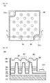
- FIG. 1A shows a top surface of a light emitting device 100 according to a first embodiment.
- FIG. 1B is a cross-sectional view of the light emitting device 100 taken along a line a-a' shown in FIG. 1A .
- FIG. 1C is an electron microscope photograph enlarging the ⁇ B1' area shown in FIG. 1B .
- FIG. 1D is a view enlarging the AA' area shown in FIG. 1B .
- Other embodiments and configurations may also be provided.
- the light emitting device 100 may include a conductive support member 110, a first conductive layer 120, a second conductive layer 130, an insulation layer 170 disposed between the first conductive layer 10 and the second conductive layer 130, and a light emitting structure.
- the conductive support member 110 may include at least one of Au, Ni, Al, Cu, W, Si, Se or GaAs.
- the conductive support member 110 may be made of a metal alloy of Si and Al.
- the light emitting structure may include a first semiconductor layer 140, a second semiconductor layer 150 and an active layer 160 disposed between the first semiconductor layer 140 and the second semiconductor layer 150.
- the first conductive layer 120 is an n-type conductive layer
- the second conductive layer 130 is a p-type conductive layer
- the first semiconductor layer 140 is an n-type semiconductor layer
- the second semiconductor layer 150 is a p-type semiconductor layer.
- the n-type conductive layer 120 may be formed on the conductive support member 110 and may include at least one conductive via 120a that has an inclined slope.
- the n-type conductive layer 120 may include at least one of Al, Au, Pt, Ti, Cr or W.
- the conductive via 120a may pass (or penetrate) through the p-type conductive layer 130, the p-type semiconductor layer 150 and the active layer 160 from the n-type conductive layer 120, and pass (or project) into the n-type semiconductor layer 140. That is, the n-type conductive layer 120 may pass (or penetrate) through the p-type conductive layer 130, the p-type semiconductor layer 150 and the active layer 160 and may include the conductive via 120a disposed in the n-type semiconductor layer 140. A top surface (or first surface) of the conductive via 120a may contact the n-type semiconductor layer 140.
- the conductive support member 110 may be electrically connected to the n-type semiconductor layer 140 through the conductive via 120a of the n-type conductive layer 120. Since the n-type conductive layer 120 is electrically connected to the conductive support member 110 and the n-type semiconductor layer 140, the n-type conductive layer 120 may be constituted by a material having a minimum contact resistance with the conductive support member 110 and the n-type semiconductor layer 140.
- the top surface B 1 of the n-type semiconductor layer 140 and at least a portion of the top surface B2 of the conductive via 120a contacting directly with the n-type semiconductor layer 140 may respectively have a surface roughness.
- the surface roughness may have a cycle in a micro unit. However, the cycle is not limited to this.
- the surface roughness may be non-uniformly formed. Since the top surface B2 of the conductive via 120a is formed to have the surface roughness, an ohmic contact surface of the n-type semiconductor layer 140 may have the surface roughness.
- the contact resistance may be reduced due to the surface area increase caused by the surface roughness of the ohmic contact surface and the surface roughness of the top surface B2 of the conductive via 120a. Therefore, the ohmic contact characteristics of the light emitting device 100 may be improved.
- the roughness of the surface may change a critical angle of light and allow the light to be easily extracted so that the light-extraction efficiency of the light emitting device 100 may be improved.
- a reflective layer 175 may be provided on an inner surface of the conductive via 120a in such a manner as to surround the conductive via 120a.
- the reflective layer 175 may be formed by including at least one of Ag, Al, Pt, Ni, Pt, Pd, Au, Ir or a transparent conductive oxide.
- the transparent conductive oxide may include ITO and GZO.
- the reflective layer 175 may be formed on a lateral surface of the conductive via 120a, and may then improve the light-extraction efficiency of an electrode of the conductive via 120a.
- the insulation layer 170 may be formed such that the n-type conductive layer 120 is electrically insulated from layers other than the conductive support member 110 and the n-type semiconductor layer 140. More specifically, the insulation layer 170 is formed between the n-type conductive layer 120 and the p-type conductive layer 130 and on the reflective layer 175, so that the n-type conductive layer 120 is electrically insulated from the p-type conductive layer 130, the p-type semiconductor layer 150 and the active layer 160. That is, the insulation layer 170 between the n-type conductive layer 120 and the p-type conductive layer 130 may be formed extending to the side wall of the conductive via 120a.
- the insulation layer 170 may be formed to include at least one of silicon oxide (SiO 2 ), silicon nitride (SiO x N y , Si x N y ), metal oxide (Al 2 O 3 ) or fluoride based compound.
- the p-type conductive layer 130 is formed on the insulation layer 170.
- the p-type conductive layer 130 may not be present in some areas through which the via electrode area B1 penetrates.
- the p-type conductive layer 130 may be formed to include at least one of Ag, Al, Pt, Ni, Pt, Pd, Au, Ir or a transparent conductive oxide (ITO and GZO).
- ITO and GZO transparent conductive oxide
- the p-type conductive layer 130 may include at least one exposed area of the interface on which the p-type conductive layer 130 contacts the p-type semiconductor layer 150.
- P-type electrode pads 131a and 131b may be formed on the exposed area in order to connect an external power supply to the p-type conductive layer 130.
- the p-type semiconductor layer 150, the active layer 160 and the n-type semiconductor layer 140 may not be formed on the exposed area.
- the p-type electrode pads 131a and 131b may be formed in a corner of the light emitting device 100, so that the light emitting area of the light emitting device 100 can be maximized.
- the active layer 160 exposed outward may function as a current leakage path during operation of the light emitting device 100. Such a problem may be prevented by forming a passivation layer 180 on a side wall of the light emitting structure.
- the passivation layer 180 may protect the light emitting structure, especially the active layer 160 from the outside and prevent a leakage current from flowing.
- the passivation layer 180 may be formed to include at least one of silicon oxide (SiO 2 ), silicon nitride (SiO x N y , Si x N y ), metal oxide (Al 2 O 3 ) or fluoride based compound.
- the p-type semiconductor layer 150 is formed on the p-type conductive layer 130.
- the active layer 160 is formed on the p-type semiconductor layer 150.
- the n-type semiconductor layer 140 is formed on the active layer 160.
- the n-type semiconductor layer 140 is formed of a semiconductor material having an empirical formula of In x Al y Ga 1-x-y N (0 ⁇ x ⁇ 1, 0 ⁇ y ⁇ 1, 0 ⁇ x+y ⁇ 1), for example, InAlGaN, GaN, AlGaN, InGaN, AlInN, AIN and InN and the like.
- An n-type dopant such as Si, Ge and Sn and/or the like may be doped on the n-type semiconductor layer 140.
- the p-type semiconductor layer 150 may be formed of a semiconductor material having an empirical formula of In x Al y Ga 1-x-y N (0 ⁇ x ⁇ 1, 0 ⁇ y ⁇ 1, 0 ⁇ x+y ⁇ 1), for example, InAlGaN, GaN, AlGaN, InGaN, AlInN, AIN and InN and/or the like.
- a p-type dopant such as Mg and Zn and/or the like may be doped on the p-type semiconductor layer 150.
- the active layer 160 is formed of a semiconductor material having an empirical formula of In x Al y Ga 1-x-y N (0 ⁇ x ⁇ 1, 0 ⁇ y ⁇ 1, 0 ⁇ x+y ⁇ 1).
- the active layer 160 may be formed by stacking a plurality of well layers and a plurality of barrier layers, for example, at a cycle of InGaN well layer/GaN barrier layer.
- the active layer 160 may be formed of another material in accordance with the material constituting the n-type semiconductor layer 140 and the p-type semiconductor layer 150. In other words, the active layer 160 may convert energy by recombination of electrons and holes into light. Therefore, the active layer 160 may be formed of a material having an energy band gap smaller than those of the n-type semiconductor layer 140 and the p-type semiconductor layer 150.
- FIG. 2A shows a top surface of a light emitting device 200 according to a second embodiment.
- FIG. 2B shows cross-sections of the light emitting device 200 that are taken along lines a-a' and b-b' shown in FIG. 2A .
- FIG. 2B shows not only the sectional structure of the light emitting device 200 taken along the line a-a' but also the sectional structure of a recess Bb1 (or etching hole) taken along the line b-b'.
- the light emitting device 200 may include a conductive support member 210, a first conductive layer 220, a second conductive layer 230, an insulation layer 270 between the first conductive layer 220 and the second conductive layer 230, and a light emitting structure.
- the conductive support member 210 may be formed to include at least one of Au, Ni, Al, Cu, W, Si, Se or GaAs.
- the conductive support member 210 may be made of a metal alloy of Si or Al.
- the light emitting structure may include a first semiconductor layer 240, a second semiconductor layer 250 and an active layer 260 between the first semiconductor layer 240 and the second semiconductor layer 250.
- the first conductive layer 220 is an n-type conductive layer
- the second conductive layer 230 is a p-type conductive layer
- the first semiconductor layer 240 is an n-type semiconductor layer
- the second semiconductor layer 250 is a p-type semiconductor layer.
- the n-type conductive layer 220 may be formed on the conductive support member 210 and may include at least one conductive via 220a.
- the n-type conductive layer 220 may be formed to include at least one of Al, Au, Pt, Ti, Cr or W.
- the conductive via 220a may pass (or penetrate) through the p-type conductive layer 230, the p-type semiconductor layer 250 and the active layer 260 from the n-type conductive layer 220, and pass (or project) into a certain area of the n-type semiconductor layer 240. That is, the n-type conductive layer 220 may pass (or penetrate) through the p-type conductive layer 230, the p-type semiconductor layer 250 and the active layer 260 and may include the conductive via 220a disposed in the n-type semiconductor layer 240. A top surface (or first surface) of the conductive via 220a may contact the n-type semiconductor layer 240.
- the conductive via 220a may have inclined side walls.
- the conductive support member 210 may be electrically connected to the n-type semiconductor layer 240 through the n-type conductive layer 220. Since the n-type conductive layer 220 may be electrically connected to the conductive support member 210 and the n-type semiconductor layer 240, the n-type conductive layer 220 may be constituted by a material having a minimum contact resistance with the conductive support member 210 and the n-type semiconductor layer 240. As described in the first embodiment, a reflective layer may be provided on an inner surface of the conductive via 220a so as to surround the conductive via 220a.
- the insulation layer 270 may be formed such that the n-type conductive layer 220 may be electrically insulated from layers other than the conductive support member 210 and the n-type semiconductor layer 240. More specifically, the insulation layer 270 may be formed between the n-type conductive layer 220 and the p-type conductive layer 230 and on the side wall of the conductive via 220a, so that the n-type conductive layer 220 is electrically insulated from the p-type conductive layer 230, the p-type semiconductor layer 250 and the active layer 260. That is, the insulation layer 270 provided between the n-type conductive layer 220 and the p-type conductive layer 230 may extend to the side wall of the conductive via 220a.
- the insulation layer 270 may be formed to include at least one of silicon oxide (SiO 2 ), silicon nitride (SiO x N y , Si x N y ), metal oxide (Al 2 O 3 ) or fluoride based compound.
- the insulation layer 170 may substantially surround a side wall of the conductive via 220a.
- the p-type conductive layer 230 may be formed on the insulation layer 270.
- the p-type conductive layer 230 may not be present in some areas through which the conductive via 220a passes (or penetrates).
- the p-type conductive layer 230 may be formed to include at least one of Ag, Al, Pt, Ni, Pt, Pd, Au, Ir or a transparent conductive oxide (ITO and GZO). Since the p-type conductive layer 230 electrically contacts with the p-type semiconductor layer 250, not only the contact resistance of the p-type semiconductor layer 250 is minimized but also light emission efficiency may be improved by reflecting outwardly light generated from the active layer 260.
- the p-type conductive layer 230 may include at least one exposed area of the interface on which the p-type conductive layer 230 contacts the p-type semiconductor layer 250.
- P-type electrode pads 231a and 231b may be formed on the exposed area in order to connect an external power supply to the p-type conductive layer 230.
- the p-type semiconductor layer 250, the active layer 260 and the n-type semiconductor layer 240 are not formed on the exposed area.
- the p-type electrode pads 231a and 231b can be formed in a corner of the light emitting device 200, so that the light emitting area of the light emitting device 200 can be maximized.
- the active layer 260 exposed outward may function as a current leakage path during operation of the light emitting device 200. Such a problem may be prevented by forming a passivation layer 280 on the side wall of the light emitting structure.
- the passivation layer 280 may protect the light emitting structure, and especially the active layer 260, from the outside and prevent a leakage current from flowing.
- the passivation layer 280 may be formed to include at least any one of silicon oxide (SiO 2 ), silicon nitride (SiO x N y , Si x N y ), metal oxide (Al 2 O 3 ) or fluoride based compound.
- At least a portion of the top surface Ba1 of the n-type semiconductor layer 240 may have a surface roughness in a micro unit. At least a part of the upper portion of the n-type semiconductor layer 240 may include at least one recess Bb1 (or etching hole) formed therein. The bottom surface of the recess Bb1 may have the surface roughness in a micro unit. As shown in FIG. 2A , the recess Bb1 may be provided between a conductive via electrode BB' and an electrode. The surface roughness may be a roughness structure. The roughness structure may be provided on at least a portion of the top surface of the first semiconductor layer and the bottom surface of the recess Bb1.
- a top surface of the semiconductor layer 240 may include a first surface area and a second surface area each having a surface roughness.
- a recess may be provided between the first surface area and the second surface area, and may have a bottom surface that has a surface roughness.
- the surface roughness of the top surface Ba1 of the n-type semiconductor layer 240, the surface roughness of the bottom surface Bb1 of the recess Bb1, and the structure itself of the recess Bb1 may change the critical angle of light and allow the light to be easily extracted, so that the light-extraction efficiency of the light emitting device 200 may be improved.
- the recess Bb1 may be uniformly arranged between the conductive via electrodes BB' and electrodes, and then light may be more uniformly emitted.
- the p-type semiconductor layer 250 is formed on the p-type conductive layer 230.
- the active layer 260 is formed on the p-type semiconductor layer 250.
- the n-type semiconductor layer 240 is formed on the active layer 260.
- the n-type semiconductor layer 240 is formed of a semiconductor material having an empirical formula of In x Al y Ga 1-x-y N (0 ⁇ x ⁇ 1, 0 ⁇ y ⁇ 1, 0 ⁇ x+y ⁇ 1), for example, InAlGaN, GaN, AlGaN, InGaN, AlInN, AIN and InN and/or the like.
- An n-type dopant such as Si, Ge and Sn and/or the like may be doped on the n-type semiconductor layer 240.
- the p-type semiconductor layer 250 may be formed of a semiconductor material having an empirical formula of In x Al y Ga 1-x-y N (0 ⁇ x ⁇ 1, 0 ⁇ y ⁇ 1, 0 ⁇ x+y ⁇ 1), for example, InAlGaN, GaN, AlGaN, InGaN, AlInN, AIN and InN and/or the like.
- a p-type dopant such as Mg and Zn and/or the like may be doped on the p-type semiconductor layer 250.
- the active layer 260 may be formed in any one of a single quantum well structure, a multiple quantum well (MQW) structure, a quantum wire structure and/or a quantum dot structure.
- the structure of the active layer 260 is not limited to this.
- the active layer 260 may be formed of a semiconductor material having an empirical formula of In x Al y Ga 1-x-y N (0 ⁇ x ⁇ 1, 0 ⁇ y ⁇ 1, 0 ⁇ x+y ⁇ 1).
- the active layer 260 is formed in the multiple quantum well (MQW) structure, the active layer 260 is formed by stacking a plurality of well layers and a plurality of barrier layers, for example, at a cycle of InGaN well layer/GaN barrier layer.
- the active layer 260 may be formed of another material in accordance with the material constituting the n-type semiconductor layer 240 and the p-type semiconductor layer 250. In other words, the active layer 260 may convert energy by recombination of electrons and holes into light. Therefore, the active layer 260 may be formed of a material having an energy band gap smaller than those of the n-type semiconductor layer 240 and the p-type semiconductor layer 250.
- FIG. 3A shows a top surface of a light emitting device 300 according to a third embodiment.
- FIG. 3B shows cross-sections of the light emitting device 300 taken along lines a-a' and b-b' shown in FIG. 3A .
- FIG. 3B shows not only the sectional structure of the light emitting device 300 taken along the line a-a' but also the sectional structure of a recess Bb2 taken along the line b-b'.
- FIG. 3C is a view enlarging the CC' area shown in FIG. 3B .
- Other embodiments and configurations may also be provided.
- the light emitting device 300 may include a conductive support member 310, a first conductive layer 320, a second conductive layer 330, an insulation layer 370 disposed between the first conductive layer 320 and the second conductive layer 330, and a light emitting structure.
- the conductive support member 310 may be formed to include at least one of Au, Ni, Al, Cu, W, Si, Se or GaAs.
- the conductive support member 310 may be made of a metal alloy of Si and Al.
- the light emitting structure may include a first semiconductor layer 340, a second semiconductor layer 350 and an active layer 360 between the first semiconductor layer 340 and the second semiconductor layer 350.
- first conductive layer 320 is an n-type conductive layer
- second conductive layer 330 is a p-type conductive layer
- first semiconductor layer 340 is an n-type semiconductor layer
- second semiconductor layer 350 is a p-type semiconductor layer.
- the n-type conductive layer 320 may be formed on the conductive support member 310 and may include at least one conductive via 320a that has an inclined slope.
- the n-type conductive layer 320 may be formed to include at least one of Al, Au, Pt, Ti, Cr or W.
- the conductive via 320a may pass (or penetrate) through the p-type conductive layer 330, the p-type semiconductor layer 350 and the active layer 360 from the n-type conductive layer 320, and may pass (or project) into the certain area of the n-type semiconductor layer 340. That is, the n-type conductive layer 320 may pass through the p-type conductive layer 330, the p-type semiconductor layer 350 and the active layer 360 and may include the conductive via 320a disposed in the n-type semiconductor layer 340. A top surface (or first surface) of the conductive via 320a may contact the n-type semiconductor layer 340.
- the conductive support member 310 may be electrically connected to the n-type semiconductor layer 340 through the n-type conductive layer 320. Since the n-type conductive layer 320 is electrically connected to the conductive support member 310 and the n-type semiconductor layer 340, the n-type conductive layer 320 may be constituted by a material having a minimum contact resistance with the conductive support member 310 and the n-type semiconductor layer 340.
- a portion of the top surface Ba2 of the conductive via 320a directly contacting with the n-type semiconductor layer 340 may have a surface roughness in a micro unit. Since the portion of the top surface B2 of the conductive via 320a is formed to have the surface roughness, an ohmic contact surface of the n-type semiconductor layer 340 may have the surface roughness.
- the contact resistance may be reduced due to the surface area increase caused by the surface roughness of the ohmic contact surface and the surface roughness of the top surface B2 of the conductive via 320a. Therefore, the ohmic contact characteristics of the light emitting device 300 may be improved.
- a first surface area and a second surface area of the top surface Ba1 of the n-type semiconductor layer 340 may have a surface roughness in a micro unit.
- the upper portion of the n-type semiconductor layer 340 may include at least recess Bb1 (or etching hole) formed therein.
- the recess Bb1 may be provided between the first surface area and the second surface area.
- the bottom surface of the recess Bb1 may also have the surface roughness in a micro unit. As shown in FIG. 3A , the recess Bb1 is provided between a conductive via electrode CC' and an electrode.
- the surface roughness of the top surface Ba1 of the n-type semiconductor layer 340, the surface roughness of the bottom surface of the recess Bb1, the surface roughness of the top surface B2 of the conductive via 320a, and the structure itself of the recess Bb1 may change the critical angle of light and allow the light to be easily extracted, so that the light-extraction efficiency of the light emitting device 300 can be improved.
- the recesses Bb1 may be uniformly arranged between the conductive via electrodes CC' and electrodes, and then light may be more uniformly emitted.
- a reflective layer 375 may be provided on the inner surface of the conductive via 320a in such a manner as to surround the conductive via 320a.
- the reflective layer 375 may be formed to include at least one of Ag, Al, Pt, Ni, Pt, Pd, Au, Ir or a transparent conductive oxide.
- the transparent conductive oxide may include ITO and GZO.
- the reflective layer 375 may be formed on a lateral surface of the conductive via 320a, and may then improve the light-extraction efficiency of an electrode of the conductive via 320a.
- the insulation layer 370 may be formed such that the n-type conductive layer 320 is electrically insulated from layers other than the conductive support member 310 and the n-type semiconductor layer 340. More specifically, the insulation layer 370 may be formed between the n-type conductive layer 320 and the p-type conductive layer 330 and on the reflective layer 375 so that the n-type conductive layer 320 is electrically insulated from the p-type conductive layer 330, the p-type semiconductor layer 350 and the active layer 360. That is, the insulation layer 370 between the n-type conductive layer 320 and the p-type conductive layer 330 may be formed extending to the side wall of the conductive via 320a.
- Such an insulation layer 370 may be formed to include at least any one of silicon oxide (SiO 2 ), silicon nitride (SiO x N y , Si x N y ), metal oxide (Al 2 O 3 ) or fluoride based compound.
- the p-type conductive layer 330 is formed on the insulation layer 370.
- the p-type conductive layer 330 may not be present in some areas through which the via electrode area B1 passes.
- the p-type conductive layer 330 may be formed to include at least one of Ag, Al, Pt, Ni, Pt, Pd, Au, Ir or a transparent conductive oxide (ITO and GZO). Since the p-type conductive layer 330 electrically contacts the p-type semiconductor layer 350, not only the contact resistance of the p-type semiconductor layer 350 is minimized but also light emission efficiency is improved by reflecting outwardly light generated from the active layer 360.
- the p-type conductive layer 330 may include at least one exposed area of the interface on which the p-type conductive layer 330 contacts the p-type semiconductor layer 350.
- P-type electrode pads 331a and 331b may be formed on the exposed area in order to connect an external power supply to the p-type conductive layer 330.
- the p-type semiconductor layer 350, the active layer 360 and the n-type semiconductor layer 340 are not formed on the exposed area.
- the p-type electrode pads 331a and 331b may be formed in a corner of the light emitting device 300, so that the light emitting area of the light emitting device 300 may be maximized.
- the active layer 360 may be exposed outward to function as a current leakage path during operation of the light emitting device 300. Such a problem may be prevented by forming a passivation layer 380 on the side wall of the light emitting structure.
- the passivation layer 380 may protect the light emitting structure, and especially the active layer 360, from the outside, and may prevent a leakage current from flowing.
- the passivation layer 380 may be formed to include at least one of silicon oxide (SiO 2 ), silicon nitride (SiO x N y , Si x N y ), metal oxide (Al 2 O 3 ) or fluoride based compound.
- the p-type semiconductor layer 350 is formed on the p-type conductive layer 330.
- the active layer 360 is formed on the p-type semiconductor layer 350.
- the n-type semiconductor layer 340 is formed on the active layer 160.
- the active layer 360 may be formed of another material in accordance with the material constituting the n-type semiconductor layer 340 and the p-type semiconductor layer 350.
- the active layer 360 may convert energy by recombination of electrons and holes into light. Therefore, the active layer 360 may be formed of a material having an energy band gap smaller than those of the n-type semiconductor layer 340 and the p-type semiconductor layer 350.
- the light-extraction efficiency by photon scattering may be improved.
- the size and the depth of the recess Bb1 may be variously determined according to arrangement of the conductive via 320a and thickness of the n-type semiconductor layer 340.
- the diameter of the bottom surface of the recess Bb1 may be formed to be equal to or larger than 5 um and equal to or less than 50 ⁇ m.
- the depth of the recess Bb1 may be formed to be 1/3 to 1/2 of a thickness of the n-type semiconductor layer 340.
- the thickness of the n-type semiconductor layer 340 may be measured in a portion (i.e., the first surface area or the second surface area) having no recess (or etching hole) formed therein and may extend from the surface of the active layer 360 to the surface of the n-type semiconductor layer 340.
- the reflective layer formed on a lateral surface of the conductive via 320a may improve the light-extraction efficiency.
- the ohmic contact characteristics may be more improved due to the surface area increase caused by the surface roughness of the ohmic contact surface and the surface roughness of the top surface of the conductive via 320a.
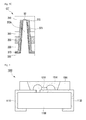
- FIG. 4 shows a light emitting device package 1000.
- the light emitting device package 1000 may include a package body 1100, a first electrode 1110, a second electrode 1120, a light emitting device 1200 and a filler 1300.
- the package body 1100 may be formed to include a silicon material, a synthetic resin material or a metallic material. Inclined surfaces may be formed around the light emitting device 1200, thereby improving the light-extraction efficiency.
- the first electrode 1110 and the second electrode 1120 may be provided in the package body 1100.
- the first electrode 1110 and the second electrode 1120 may be electrically isolated from each other and may supply electric power to the light emitting device 1200.
- the first electrode 1110 and the second electrode 1120 may reflect light generated from the light emitting device 1200 and increase luminous efficiency.
- the first electrode 1110 and the second electrode 1120 may also exhaust heat generated from the light emitting device 1200.
- the light emitting device 1200 may be electrically connected to the first electrode1110 and the second electrode 1120.
- the light emitting device 1200 may be provided on the package body 1100 or may be provided on either the first electrode 1110 or the second electrode 1120.
- the light emitting device 1200 may also be electrically connected to the first electrode 1110 and the second electrode 1120 in a wire bonding manner or in a flip-chip manner and in a die-bonding process.
- the filler 1300 may be formed to surround and protect the light emitting device 1200.
- the filler 1300 may include a fluorescent material and may change the wavelength of light emitted from the light emitting device 1200.
- the light emitting device package 1000 may be equipped with one or a plurality of the light emitting devices disclosed in the above embodiments. There is no limited to the number of the light emitting devices.
- a plurality of the light emitting device packages 1000 may be arrayed on the support member.
- An optical member (such as a light guide plate, a prism sheet and a diffusion sheet and/or the like) may be provided on the optical path of the light emitting device package 1000.
- Such a light emitting device package 1000, the support member and the optical member may function as a light unit.
- Another embodiment may be implemented by a display device, a pointing device, a backlight unit, a lighting device and/or the like, all of which may include the semiconductor light emitting device or the light emitting device package that has been described in the aforementioned embodiments.
- the lighting device may include a lamp and a street lamp.
- FIG. 5 is a view showing a lighting system 1500 that includes the light emitting device package according to the aforementioned embodiment.
- the lighting system 1500 may include a case 1510, a light emitting module 1530 disposed in the case 1510, and a connection terminal 1520 disposed in the case 1510 and supplied with an electric power from an external power supply.
- the case 1510 may be formed of a material having an excellent heat radiating characteristic, for example, a metal material or a resin material.
- the light emitting module 1530 may include a board 1532 and at least one light emitting device package 30 that is based on an above embodiment and is mounted on the board 1532.
- the light emitting device package 30 may include a plurality of light emitting devices that are arranged apart from each other at a predetermined interval in the form of a matrix.
- the board 1532 may be an insulating substrate on which a circuit pattern has been printed, and may include, for example, a printed circuit board (PCB), a metal core PCB, a flexible PCB, a ceramic PCB, an FR-4 substrate, etc.
- PCB printed circuit board
- metal core PCB metal core PCB
- flexible PCB flexible PCB
- ceramic PCB ceramic PCB
- FR-4 substrate etc.
- the board 1532 may be formed of a material capable of efficiently reflecting light.
- the surface of the board 1532 may have a color capable of efficiently reflecting light, such as white or silver.
- the at least one light emitting device package 30 may be provided on the board 1532.
- Each of the light emitting device packages 30 may include at least one light emitting diode (LED) chip.
- the LED chip may include both a LED emitting red, green, blue or white light and a UV LED emitting ultraviolet (UV).
- the light emitting module 1530 may have various combinations of the light emitting device packages so as to obtain desired color and luminance.
- the light emitting module 1530 may have a combination of a white LED, a red LED and a green LED in order to obtain a high color rendering index (CRI).
- CRI color rendering index
- connection terminal 1520 may be electrically connected to the light emitting module 1530 in order to supply power.
- the connection terminal 1520 may be screwed and connected to an external power in the form of a socket.
- the connection terminal 1520 may be made in the form of a pin and inserted into the external power, and/or may be connected to the external power through a power line.
- a light emitting device may include: a conductive support member; a first conductive layer disposed on the conductive support member; a second conductive layer disposed on the first conductive layer; an insulation layer disposed between the first conductive layer and the second conductive layer; and a light emitting structure being disposed on the second conductive layer, and including a second semiconductor layer, a first semiconductor layer disposed on the second semiconductor layer, and an active layer disposed between the first semiconductor layer and the second semiconductor layer.
- the first conductive layer may include at least one conductive via that penetrates through the second conductive layer, the second semiconductor layer and the active layer, and is disposed in the first semiconductor layer.
- the insulation layer may be formed to extend to the side wall of the conductive via.
- At least one recess may be formed in the upper portion of the first semiconductor layer. At least a portion of the top surface of the first semiconductor layer and the bottom surface of the recess may have a surface roughness.
- a light emitting device package may include: a package body; a first electrode layer and a second electrode layer disposed on the package body; and a light emitting device electrically connected to the first electrode layer and the second electrode layer.
- a lighting apparatus may include the light emitting device package.
- the light emitting device may further include a reflective layer located between the side wall of the conductive via and the insulation layer formed on the side wall of the conductive via.
- the reflective layer may include at least one of Ag, Al, Pt, Ni, Pt, Pd, Au, Ir or a transparent conductive oxide, and wherein the transparent conductive oxide includes at least one of ITO and/or GZO.
- the top surface of the conductive via may have an area greater than that of the bottom surface of the conductive via.
- the second conductive layer may include at least one exposed area of surface forming an interface with the second semiconductor layer, and wherein the light emitting device may further include an electrode pad formed on the exposed area of the second conductive layer. The electrode pad may be formed in the corner of the light emitting device.
- the light emitting device may further include a passivation layer formed on the side wall of the light emitting structure, in order to prevent a leakage current from flowing through the active layer.
- the insulation layer and the passivation layer are respectively formed including at least one of silicon oxide (SiO2), silicon nitride (SiOxNy, SixNy), metal oxide (Al2O3) or fluoride based compound.
- the conductive support member may include at least one of Au, Ni, Al, Cu, W, Si, Se or GaAs.
- the first conductive layer may include at least one of Al, Au, Pt, Ti, Cr or W.
- the second conductive layer reflects light generated from the active layer.
- the second conductive layer may include at least one of Ag, Al, Pt, Ni, Pt, Pd, Au, Ir or a transparent conductive oxide, and wherein the transparent conductive oxide includes at least one of ITO and/or GZO.
- the recess or etching hole is disposed between the conductive vias.
- the at least a portion of the top surface of the conductive via contacting with the first semiconductor layer has a roughness surface.
- the distance between the conductive vias may be equal to or larger than 5 ⁇ m and equal to or less than 50 ⁇ m.
- the distance from the bottom surface of the first semiconductor layer to the bottom surface of the etching hole may be 1/2 to 2/3 of a thickness of the first semiconductor layer.
- the diameter of the bottom surface of the recess or the etching hole may be equal to or larger than 5 ⁇ m and equal to or less than 50 ⁇ m.
- the depth of the recess or the etching hole may be 1/3 to 1/2 of a thickness of the first semiconductor layer.
- any reference in this specification to "one embodiment,” “an embodiment,” “example embodiment,” etc. means that a particular feature, structure, or characteristic described in connection with the embodiment is included in at least one embodiment of the invention.
- the appearances of such phrases in various places in the specification are not necessarily all referring to the same embodiment.
Abstract
Description
- Embodiments may relate to a light emitting device.
- A light emitting diode (LED) is a semiconductor element for converting electric energy into light. As compared with existing light sources such as a fluorescent lamp and an incandescent electric lamp, the LED may have advantages of low power consumption, a semi-permanent span of life, a rapid response speed, safety and/or an environmental-friendliness. Research may be devoted to substitution of existing light sources with the LED. The LED may be used as a light source for lighting devices, for example, various lamps used interiorly and exteriorly, a liquid crystal display device, an electric sign and a street lamp and/or the like.
- A vertical LED device may be developed that is different from previous LED devices and may have upper and lower electrodes formed therein. In the vertical LED device, since electric current flows from top to bottom, the electric current may be uniformly injected and distributed throughout an entire area of the device. Therefore, the vertical LED device may have a low operating voltage and an excellent current uniformity in an active area.
- When the vertical LED device is applied to a high-power application such as a display, an inner/outer lighting module and a lighting and the like, thermal properties may be improved and a design suitable for the thermal properties may be developed. The vertical LED device may have advantages of removing a sapphire substrate having a low thermal conductivity, of improving thermal resistance by inserting a metallic electrode, and/or of increasing product life span.
- Arrangements and embodiments may be described in detail with reference to the following drawings in which like reference numerals refer to like elements and wherein:
-
FIG. 1A shows a top surface of a light emitting device according to a first embodiment; -
FIG. 1B is a cross-sectional view of the light emitting device taken along a line a-a' shown inFIG. 1A ; -
FIG. 1C is an electron microscope photograph enlarging the `B1' area shown inFIG. 1B ; -
FIG. 1D is a view enlarging the AA' area shown inFIG. 1B ; -
FIG. 2A shows a top surface of a light emitting device according to a second embodiment; -
FIG. 2B shows cross-sections of the light emitting device taken along lines a-a' and b-b' shown inFIG. 2A ; -
FIG. 3A shows a top surface of a light emitting device according to a third embodiment; -
FIG. 3B shows cross-sections of the light emitting device taken along lines a-a' and b-b' shown inFIG. 3A ; -
FIG. 3C is a view enlarging the CC' area shown inFIG. 3B ; -
FIG. 4 shows a light emitting device package; and -
FIG. 5 is a view showing a lighting system including the light emitting device package. - Embodiments may be described in detail with reference to accompanying drawings. However, the accompanied drawings are provided only for more easily describing the embodiments. It may be understood by those skilled in the art that the spirit and scope of embodiments is not limited to the scope of the accompanied drawings.
- A thickness or a size of each layer may be magnified, omitted or schematically shown for the purpose of convenience and clearness of description. The size of each component does not necessarily mean its actual size.
- It will be understood that when an element is referred to as being 'on' or 'under' another element, it may be directly on/under the element, and one or more intervening elements may also be present. When an element is referred to as being `on' or 'under', 'under the element' as well as 'on the element' may be included based on the element.
- An embodiment may be described in detail with reference to the accompanying drawings.
- First embodiment
-
FIG. 1A shows a top surface of alight emitting device 100 according to a first embodiment.FIG. 1B is a cross-sectional view of thelight emitting device 100 taken along a line a-a' shown inFIG. 1A .FIG. 1C is an electron microscope photograph enlarging the `B1' area shown inFIG. 1B .FIG. 1D is a view enlarging the AA' area shown inFIG. 1B . Other embodiments and configurations may also be provided. - Referring to
FIGs. 1A, 1B and1D , thelight emitting device 100 according may include aconductive support member 110, a firstconductive layer 120, a secondconductive layer 130, aninsulation layer 170 disposed between the first conductive layer 10 and the secondconductive layer 130, and a light emitting structure. - The
conductive support member 110 may include at least one of Au, Ni, Al, Cu, W, Si, Se or GaAs. For example, theconductive support member 110 may be made of a metal alloy of Si and Al. - The light emitting structure may include a
first semiconductor layer 140, asecond semiconductor layer 150 and anactive layer 160 disposed between thefirst semiconductor layer 140 and thesecond semiconductor layer 150. - For ease of convenience, it is assumed that the first
conductive layer 120 is an n-type conductive layer, the secondconductive layer 130 is a p-type conductive layer, thefirst semiconductor layer 140 is an n-type semiconductor layer, and thesecond semiconductor layer 150 is a p-type semiconductor layer. - The n-type
conductive layer 120 may be formed on theconductive support member 110 and may include at least one conductive via 120a that has an inclined slope. The n-typeconductive layer 120 may include at least one of Al, Au, Pt, Ti, Cr or W. - The conductive via 120a may pass (or penetrate) through the p-type
conductive layer 130, the p-type semiconductor layer 150 and theactive layer 160 from the n-typeconductive layer 120, and pass (or project) into the n-type semiconductor layer 140. That is, the n-typeconductive layer 120 may pass (or penetrate) through the p-typeconductive layer 130, the p-type semiconductor layer 150 and theactive layer 160 and may include the conductive via 120a disposed in the n-type semiconductor layer 140. A top surface (or first surface) of the conductive via 120a may contact the n-type semiconductor layer 140. Accordingly, theconductive support member 110 may be electrically connected to the n-type semiconductor layer 140 through the conductive via 120a of the n-typeconductive layer 120. Since the n-typeconductive layer 120 is electrically connected to theconductive support member 110 and the n-type semiconductor layer 140, the n-typeconductive layer 120 may be constituted by a material having a minimum contact resistance with theconductive support member 110 and the n-type semiconductor layer 140. - As shown in
FIG. 1C , the top surface B 1 of the n-type semiconductor layer 140 and at least a portion of the top surface B2 of the conductive via 120a contacting directly with the n-type semiconductor layer 140 may respectively have a surface roughness. The surface roughness may have a cycle in a micro unit. However, the cycle is not limited to this. The surface roughness may be non-uniformly formed. Since the top surface B2 of the conductive via 120a is formed to have the surface roughness, an ohmic contact surface of the n-type semiconductor layer 140 may have the surface roughness. - As such, the contact resistance may be reduced due to the surface area increase caused by the surface roughness of the ohmic contact surface and the surface roughness of the top surface B2 of the conductive via 120a. Therefore, the ohmic contact characteristics of the
light emitting device 100 may be improved. - In the surface roughness of the top surface B1 of the n-
type semiconductor layer 140 and the surface roughness of the top surface B2 of the conductive via 120a, the roughness of the surface may change a critical angle of light and allow the light to be easily extracted so that the light-extraction efficiency of thelight emitting device 100 may be improved. - A
reflective layer 175 may be provided on an inner surface of the conductive via 120a in such a manner as to surround the conductive via 120a. Thereflective layer 175 may be formed by including at least one of Ag, Al, Pt, Ni, Pt, Pd, Au, Ir or a transparent conductive oxide. The transparent conductive oxide may include ITO and GZO. Thereflective layer 175 may be formed on a lateral surface of the conductive via 120a, and may then improve the light-extraction efficiency of an electrode of the conductive via 120a. - The
insulation layer 170 may be formed such that the n-typeconductive layer 120 is electrically insulated from layers other than theconductive support member 110 and the n-type semiconductor layer 140. More specifically, theinsulation layer 170 is formed between the n-typeconductive layer 120 and the p-typeconductive layer 130 and on thereflective layer 175, so that the n-typeconductive layer 120 is electrically insulated from the p-typeconductive layer 130, the p-type semiconductor layer 150 and theactive layer 160. That is, theinsulation layer 170 between the n-typeconductive layer 120 and the p-typeconductive layer 130 may be formed extending to the side wall of the conductive via 120a. Theinsulation layer 170 may be formed to include at least one of silicon oxide (SiO2), silicon nitride (SiOxNy, SixNy), metal oxide (Al2O3) or fluoride based compound. - The p-type
conductive layer 130 is formed on theinsulation layer 170. The p-typeconductive layer 130 may not be present in some areas through which the via electrode area B1 penetrates. The p-typeconductive layer 130 may be formed to include at least one of Ag, Al, Pt, Ni, Pt, Pd, Au, Ir or a transparent conductive oxide (ITO and GZO). Through this, since the p-typeconductive layer 130 electrically contacts with the p-type semiconductor layer 150, not only the contact resistance of the p-type semiconductor layer 150 is minimized but also light emission efficiency is improved by reflecting outwardly light generated from theactive layer 160. - The p-type
conductive layer 130 may include at least one exposed area of the interface on which the p-typeconductive layer 130 contacts the p-type semiconductor layer 150. P-type electrode pads conductive layer 130. The p-type semiconductor layer 150, theactive layer 160 and the n-type semiconductor layer 140 may not be formed on the exposed area. The p-type electrode pads light emitting device 100, so that the light emitting area of thelight emitting device 100 can be maximized. - The
active layer 160 exposed outward may function as a current leakage path during operation of thelight emitting device 100. Such a problem may be prevented by forming apassivation layer 180 on a side wall of the light emitting structure. Thepassivation layer 180 may protect the light emitting structure, especially theactive layer 160 from the outside and prevent a leakage current from flowing. Thepassivation layer 180 may be formed to include at least one of silicon oxide (SiO2), silicon nitride (SiOxNy, SixNy), metal oxide (Al2O3) or fluoride based compound. - The p-
type semiconductor layer 150 is formed on the p-typeconductive layer 130. Theactive layer 160 is formed on the p-type semiconductor layer 150. The n-type semiconductor layer 140 is formed on theactive layer 160. - The n-
type semiconductor layer 140 is formed of a semiconductor material having an empirical formula of InxAlyGa1-x-yN (0≤x≤1, 0 ≤y≤1, 0≤x+y≤1), for example, InAlGaN, GaN, AlGaN, InGaN, AlInN, AIN and InN and the like. An n-type dopant such as Si, Ge and Sn and/or the like may be doped on the n-type semiconductor layer 140. - The p-
type semiconductor layer 150 may be formed of a semiconductor material having an empirical formula of InxAlyGa1-x-yN (0≤x≤1, 0 ≤y≤1, 0≤x+y≤1), for example, InAlGaN, GaN, AlGaN, InGaN, AlInN, AIN and InN and/or the like. A p-type dopant such as Mg and Zn and/or the like may be doped on the p-type semiconductor layer 150. - The
active layer 160 is formed of a semiconductor material having an empirical formula of InxAlyGa1-x-yN (0≤x≤1, 0 ≤y≤1, 0≤x+y≤1). When theactive layer 160 is formed in a multiple quantum well (MQW) structure, theactive layer 160 may be formed by stacking a plurality of well layers and a plurality of barrier layers, for example, at a cycle of InGaN well layer/GaN barrier layer. - The
active layer 160 may be formed of another material in accordance with the material constituting the n-type semiconductor layer 140 and the p-type semiconductor layer 150. In other words, theactive layer 160 may convert energy by recombination of electrons and holes into light. Therefore, theactive layer 160 may be formed of a material having an energy band gap smaller than those of the n-type semiconductor layer 140 and the p-type semiconductor layer 150. - Second embodiment
-
FIG. 2A shows a top surface of alight emitting device 200 according to a second embodiment.FIG. 2B shows cross-sections of thelight emitting device 200 that are taken along lines a-a' and b-b' shown inFIG. 2A . For the purpose of understanding the sectional structure of thelight emitting device 200,FIG. 2B shows not only the sectional structure of thelight emitting device 200 taken along the line a-a' but also the sectional structure of a recess Bb1 (or etching hole) taken along the line b-b'. - Referring to
FIGs. 2A and 2B , thelight emitting device 200 may include aconductive support member 210, a first conductive layer 220, a secondconductive layer 230, an insulation layer 270 between the first conductive layer 220 and the secondconductive layer 230, and a light emitting structure. - The
conductive support member 210 may be formed to include at least one of Au, Ni, Al, Cu, W, Si, Se or GaAs. For example, theconductive support member 210 may be made of a metal alloy of Si or Al. - The light emitting structure may include a
first semiconductor layer 240, a second semiconductor layer 250 and anactive layer 260 between thefirst semiconductor layer 240 and the second semiconductor layer 250. - For ease of description, it is assumed that the first conductive layer 220 is an n-type conductive layer, the second
conductive layer 230 is a p-type conductive layer, thefirst semiconductor layer 240 is an n-type semiconductor layer, and the second semiconductor layer 250 is a p-type semiconductor layer. - The n-type conductive layer 220 may be formed on the
conductive support member 210 and may include at least one conductive via 220a. The n-type conductive layer 220 may be formed to include at least one of Al, Au, Pt, Ti, Cr or W. - The conductive via 220a may pass (or penetrate) through the p-type
conductive layer 230, the p-type semiconductor layer 250 and theactive layer 260 from the n-type conductive layer 220, and pass (or project) into a certain area of the n-type semiconductor layer 240. That is, the n-type conductive layer 220 may pass (or penetrate) through the p-typeconductive layer 230, the p-type semiconductor layer 250 and theactive layer 260 and may include the conductive via 220a disposed in the n-type semiconductor layer 240. A top surface (or first surface) of the conductive via 220a may contact the n-type semiconductor layer 240. The conductive via 220a may have inclined side walls. Accordingly, theconductive support member 210 may be electrically connected to the n-type semiconductor layer 240 through the n-type conductive layer 220. Since the n-type conductive layer 220 may be electrically connected to theconductive support member 210 and the n-type semiconductor layer 240, the n-type conductive layer 220 may be constituted by a material having a minimum contact resistance with theconductive support member 210 and the n-type semiconductor layer 240. As described in the first embodiment, a reflective layer may be provided on an inner surface of the conductive via 220a so as to surround the conductive via 220a. - The insulation layer 270 may be formed such that the n-type conductive layer 220 may be electrically insulated from layers other than the
conductive support member 210 and the n-type semiconductor layer 240. More specifically, the insulation layer 270 may be formed between the n-type conductive layer 220 and the p-typeconductive layer 230 and on the side wall of the conductive via 220a, so that the n-type conductive layer 220 is electrically insulated from the p-typeconductive layer 230, the p-type semiconductor layer 250 and theactive layer 260. That is, the insulation layer 270 provided between the n-type conductive layer 220 and the p-typeconductive layer 230 may extend to the side wall of the conductive via 220a. The insulation layer 270 may be formed to include at least one of silicon oxide (SiO2), silicon nitride (SiOxNy, SixNy), metal oxide (Al2O3) or fluoride based compound. Theinsulation layer 170 may substantially surround a side wall of the conductive via 220a. - The p-type
conductive layer 230 may be formed on the insulation layer 270. The p-typeconductive layer 230 may not be present in some areas through which the conductive via 220a passes (or penetrates). The p-typeconductive layer 230 may be formed to include at least one of Ag, Al, Pt, Ni, Pt, Pd, Au, Ir or a transparent conductive oxide (ITO and GZO). Since the p-typeconductive layer 230 electrically contacts with the p-type semiconductor layer 250, not only the contact resistance of the p-type semiconductor layer 250 is minimized but also light emission efficiency may be improved by reflecting outwardly light generated from theactive layer 260. - The p-type
conductive layer 230 may include at least one exposed area of the interface on which the p-typeconductive layer 230 contacts the p-type semiconductor layer 250. P-type electrode pads conductive layer 230. The p-type semiconductor layer 250, theactive layer 260 and the n-type semiconductor layer 240 are not formed on the exposed area. The p-type electrode pads light emitting device 200, so that the light emitting area of thelight emitting device 200 can be maximized. - The
active layer 260 exposed outward may function as a current leakage path during operation of thelight emitting device 200. Such a problem may be prevented by forming apassivation layer 280 on the side wall of the light emitting structure. Thepassivation layer 280 may protect the light emitting structure, and especially theactive layer 260, from the outside and prevent a leakage current from flowing. Thepassivation layer 280 may be formed to include at least any one of silicon oxide (SiO2), silicon nitride (SiOxNy, SixNy), metal oxide (Al2O3) or fluoride based compound. - At least a portion of the top surface Ba1 of the n-
type semiconductor layer 240 may have a surface roughness in a micro unit. At least a part of the upper portion of the n-type semiconductor layer 240 may include at least one recess Bb1 (or etching hole) formed therein. The bottom surface of the recess Bb1 may have the surface roughness in a micro unit. As shown inFIG. 2A , the recess Bb1 may be provided between a conductive via electrode BB' and an electrode. The surface roughness may be a roughness structure. The roughness structure may be provided on at least a portion of the top surface of the first semiconductor layer and the bottom surface of the recess Bb1. - A top surface of the
semiconductor layer 240 may include a first surface area and a second surface area each having a surface roughness. A recess may be provided between the first surface area and the second surface area, and may have a bottom surface that has a surface roughness. - The surface roughness of the top surface Ba1 of the n-
type semiconductor layer 240, the surface roughness of the bottom surface Bb1 of the recess Bb1, and the structure itself of the recess Bb1 may change the critical angle of light and allow the light to be easily extracted, so that the light-extraction efficiency of thelight emitting device 200 may be improved. The recess Bb1 may be uniformly arranged between the conductive via electrodes BB' and electrodes, and then light may be more uniformly emitted. - The p-type semiconductor layer 250 is formed on the p-type
conductive layer 230. Theactive layer 260 is formed on the p-type semiconductor layer 250. The n-type semiconductor layer 240 is formed on theactive layer 260. - The n-
type semiconductor layer 240 is formed of a semiconductor material having an empirical formula of InxAlyGa1-x-yN (0≤x≤1, 0 ≤y≤1, 0≤x+y≤1), for example, InAlGaN, GaN, AlGaN, InGaN, AlInN, AIN and InN and/or the like. An n-type dopant such as Si, Ge and Sn and/or the like may be doped on the n-type semiconductor layer 240. - The p-type semiconductor layer 250 may be formed of a semiconductor material having an empirical formula of InxAlyGa1-x-yN (0≤x≤1, 0≤y≤1, 0≤x+y≤1), for example, InAlGaN, GaN, AlGaN, InGaN, AlInN, AIN and InN and/or the like. A p-type dopant such as Mg and Zn and/or the like may be doped on the p-type semiconductor layer 250.
- The
active layer 260 may be formed in any one of a single quantum well structure, a multiple quantum well (MQW) structure, a quantum wire structure and/or a quantum dot structure. The structure of theactive layer 260 is not limited to this. - The
active layer 260 may be formed of a semiconductor material having an empirical formula of InxAlyGa1-x-yN (0≤x≤1, 0 ≤y≤1, 0≤x+y≤1). When theactive layer 260 is formed in the multiple quantum well (MQW) structure, theactive layer 260 is formed by stacking a plurality of well layers and a plurality of barrier layers, for example, at a cycle of InGaN well layer/GaN barrier layer. - The
active layer 260 may be formed of another material in accordance with the material constituting the n-type semiconductor layer 240 and the p-type semiconductor layer 250. In other words, theactive layer 260 may convert energy by recombination of electrons and holes into light. Therefore, theactive layer 260 may be formed of a material having an energy band gap smaller than those of the n-type semiconductor layer 240 and the p-type semiconductor layer 250. - Third embodiment
-
FIG. 3A shows a top surface of alight emitting device 300 according to a third embodiment.FIG. 3B shows cross-sections of thelight emitting device 300 taken along lines a-a' and b-b' shown inFIG. 3A . For the purpose of understanding the sectional structure of thelight emitting device 300,FIG. 3B shows not only the sectional structure of thelight emitting device 300 taken along the line a-a' but also the sectional structure of a recess Bb2 taken along the line b-b'.FIG. 3C is a view enlarging the CC' area shown inFIG. 3B . Other embodiments and configurations may also be provided. - Referring to
FIGs. 3A, 3B and3C , thelight emitting device 300 may include aconductive support member 310, a firstconductive layer 320, a secondconductive layer 330, aninsulation layer 370 disposed between the firstconductive layer 320 and the secondconductive layer 330, and a light emitting structure. - The
conductive support member 310 may be formed to include at least one of Au, Ni, Al, Cu, W, Si, Se or GaAs. For example, theconductive support member 310 may be made of a metal alloy of Si and Al. - The light emitting structure may include a
first semiconductor layer 340, asecond semiconductor layer 350 and anactive layer 360 between thefirst semiconductor layer 340 and thesecond semiconductor layer 350. For ease of description, it is assumed that the firstconductive layer 320 is an n-type conductive layer, the secondconductive layer 330 is a p-type conductive layer, thefirst semiconductor layer 340 is an n-type semiconductor layer, and thesecond semiconductor layer 350 is a p-type semiconductor layer. - The n-type
conductive layer 320 may be formed on theconductive support member 310 and may include at least one conductive via 320a that has an inclined slope. The n-typeconductive layer 320 may be formed to include at least one of Al, Au, Pt, Ti, Cr or W. - The conductive via 320a may pass (or penetrate) through the p-type
conductive layer 330, the p-type semiconductor layer 350 and theactive layer 360 from the n-typeconductive layer 320, and may pass (or project) into the certain area of the n-type semiconductor layer 340. That is, the n-typeconductive layer 320 may pass through the p-typeconductive layer 330, the p-type semiconductor layer 350 and theactive layer 360 and may include the conductive via 320a disposed in the n-type semiconductor layer 340. A top surface (or first surface) of the conductive via 320a may contact the n-type semiconductor layer 340. Accordingly, theconductive support member 310 may be electrically connected to the n-type semiconductor layer 340 through the n-typeconductive layer 320. Since the n-typeconductive layer 320 is electrically connected to theconductive support member 310 and the n-type semiconductor layer 340, the n-typeconductive layer 320 may be constituted by a material having a minimum contact resistance with theconductive support member 310 and the n-type semiconductor layer 340. - A portion of the top surface Ba2 of the conductive via 320a directly contacting with the n-
type semiconductor layer 340 may have a surface roughness in a micro unit. Since the portion of the top surface B2 of the conductive via 320a is formed to have the surface roughness, an ohmic contact surface of the n-type semiconductor layer 340 may have the surface roughness. - The contact resistance may be reduced due to the surface area increase caused by the surface roughness of the ohmic contact surface and the surface roughness of the top surface B2 of the conductive via 320a. Therefore, the ohmic contact characteristics of the
light emitting device 300 may be improved. - A first surface area and a second surface area of the top surface Ba1 of the n-
type semiconductor layer 340 may have a surface roughness in a micro unit. The upper portion of the n-type semiconductor layer 340 may include at least recess Bb1 (or etching hole) formed therein. The recess Bb1 may be provided between the first surface area and the second surface area. The bottom surface of the recess Bb1 may also have the surface roughness in a micro unit. As shown inFIG. 3A , the recess Bb1 is provided between a conductive via electrode CC' and an electrode. - The surface roughness of the top surface Ba1 of the n-
type semiconductor layer 340, the surface roughness of the bottom surface of the recess Bb1, the surface roughness of the top surface B2 of the conductive via 320a, and the structure itself of the recess Bb1 may change the critical angle of light and allow the light to be easily extracted, so that the light-extraction efficiency of thelight emitting device 300 can be improved. The recesses Bb1 may be uniformly arranged between the conductive via electrodes CC' and electrodes, and then light may be more uniformly emitted. - A
reflective layer 375 may be provided on the inner surface of the conductive via 320a in such a manner as to surround the conductive via 320a. Thereflective layer 375 may be formed to include at least one of Ag, Al, Pt, Ni, Pt, Pd, Au, Ir or a transparent conductive oxide. The transparent conductive oxide may include ITO and GZO. Thereflective layer 375 may be formed on a lateral surface of the conductive via 320a, and may then improve the light-extraction efficiency of an electrode of the conductive via 320a. - The
insulation layer 370 may be formed such that the n-typeconductive layer 320 is electrically insulated from layers other than theconductive support member 310 and the n-type semiconductor layer 340. More specifically, theinsulation layer 370 may be formed between the n-typeconductive layer 320 and the p-typeconductive layer 330 and on thereflective layer 375 so that the n-typeconductive layer 320 is electrically insulated from the p-typeconductive layer 330, the p-type semiconductor layer 350 and theactive layer 360. That is, theinsulation layer 370 between the n-typeconductive layer 320 and the p-typeconductive layer 330 may be formed extending to the side wall of the conductive via 320a. Such aninsulation layer 370 may be formed to include at least any one of silicon oxide (SiO2), silicon nitride (SiOxNy, SixNy), metal oxide (Al2O3) or fluoride based compound. - The p-type
conductive layer 330 is formed on theinsulation layer 370. The p-typeconductive layer 330 may not be present in some areas through which the via electrode area B1 passes. The p-typeconductive layer 330 may be formed to include at least one of Ag, Al, Pt, Ni, Pt, Pd, Au, Ir or a transparent conductive oxide (ITO and GZO). Since the p-typeconductive layer 330 electrically contacts the p-type semiconductor layer 350, not only the contact resistance of the p-type semiconductor layer 350 is minimized but also light emission efficiency is improved by reflecting outwardly light generated from theactive layer 360. - The p-type
conductive layer 330 may include at least one exposed area of the interface on which the p-typeconductive layer 330 contacts the p-type semiconductor layer 350. P-type electrode pads conductive layer 330. The p-type semiconductor layer 350, theactive layer 360 and the n-type semiconductor layer 340 are not formed on the exposed area. The p-type electrode pads light emitting device 300, so that the light emitting area of thelight emitting device 300 may be maximized. - The
active layer 360 may be exposed outward to function as a current leakage path during operation of thelight emitting device 300. Such a problem may be prevented by forming apassivation layer 380 on the side wall of the light emitting structure. Thepassivation layer 380 may protect the light emitting structure, and especially theactive layer 360, from the outside, and may prevent a leakage current from flowing. Thepassivation layer 380 may be formed to include at least one of silicon oxide (SiO2), silicon nitride (SiOxNy, SixNy), metal oxide (Al2O3) or fluoride based compound. - The p-
type semiconductor layer 350 is formed on the p-typeconductive layer 330. Theactive layer 360 is formed on the p-type semiconductor layer 350. The n-type semiconductor layer 340 is formed on theactive layer 160. - The
active layer 360 may be formed of another material in accordance with the material constituting the n-type semiconductor layer 340 and the p-type semiconductor layer 350. Theactive layer 360 may convert energy by recombination of electrons and holes into light. Therefore, theactive layer 360 may be formed of a material having an energy band gap smaller than those of the n-type semiconductor layer 340 and the p-type semiconductor layer 350. - According to the embodiment, due to the surface roughness of the top surface of the n-
type semiconductor layer 340, the surface roughness of the bottom surface of the recess Bb1, the surface roughness of the top surface of the conductive via 320a, the light-extraction efficiency by photon scattering may be improved. - The size and the depth of the recess Bb1 may be variously determined according to arrangement of the conductive via 320a and thickness of the n-
type semiconductor layer 340. The diameter of the bottom surface of the recess Bb1 may be formed to be equal to or larger than 5 um and equal to or less than 50 µm. The depth of the recess Bb1 may be formed to be 1/3 to 1/2 of a thickness of the n-type semiconductor layer 340. The thickness of the n-type semiconductor layer 340 may be measured in a portion (i.e., the first surface area or the second surface area) having no recess (or etching hole) formed therein and may extend from the surface of theactive layer 360 to the surface of the n-type semiconductor layer 340. The reflective layer formed on a lateral surface of the conductive via 320a may improve the light-extraction efficiency. - The ohmic contact characteristics may be more improved due to the surface area increase caused by the surface roughness of the ohmic contact surface and the surface roughness of the top surface of the conductive via 320a.
- Light emitting device package
- A light emitting device package according to an embodiment may be described with reference to
FIG. 4. FIG. 4 shows a light emittingdevice package 1000. - As shown in
FIG. 4 , the light emittingdevice package 1000 may include apackage body 1100, afirst electrode 1110, asecond electrode 1120, alight emitting device 1200 and afiller 1300. - The
package body 1100 may be formed to include a silicon material, a synthetic resin material or a metallic material. Inclined surfaces may be formed around thelight emitting device 1200, thereby improving the light-extraction efficiency. - The
first electrode 1110 and thesecond electrode 1120 may be provided in thepackage body 1100. Thefirst electrode 1110 and thesecond electrode 1120 may be electrically isolated from each other and may supply electric power to thelight emitting device 1200. Thefirst electrode 1110 and thesecond electrode 1120 may reflect light generated from thelight emitting device 1200 and increase luminous efficiency. Thefirst electrode 1110 and thesecond electrode 1120 may also exhaust heat generated from thelight emitting device 1200. - The
light emitting device 1200 may be electrically connected to the first electrode1110 and thesecond electrode 1120. Thelight emitting device 1200 may be provided on thepackage body 1100 or may be provided on either thefirst electrode 1110 or thesecond electrode 1120. - The
light emitting device 1200 may also be electrically connected to thefirst electrode 1110 and thesecond electrode 1120 in a wire bonding manner or in a flip-chip manner and in a die-bonding process. - The
filler 1300 may be formed to surround and protect thelight emitting device 1200. Thefiller 1300 may include a fluorescent material and may change the wavelength of light emitted from thelight emitting device 1200. - The light emitting
device package 1000 may be equipped with one or a plurality of the light emitting devices disclosed in the above embodiments. There is no limited to the number of the light emitting devices. - A plurality of the light emitting
device packages 1000 may be arrayed on the support member. An optical member (such as a light guide plate, a prism sheet and a diffusion sheet and/or the like) may be provided on the optical path of the light emittingdevice package 1000. Such a light emittingdevice package 1000, the support member and the optical member may function as a light unit. - Another embodiment may be implemented by a display device, a pointing device, a backlight unit, a lighting device and/or the like, all of which may include the semiconductor light emitting device or the light emitting device package that has been described in the aforementioned embodiments. For example, the lighting device may include a lamp and a street lamp.
- Lighting device
-
FIG. 5 is a view showing alighting system 1500 that includes the light emitting device package according to the aforementioned embodiment. - Referring to
FIG. 5 , thelighting system 1500 may include acase 1510, alight emitting module 1530 disposed in thecase 1510, and aconnection terminal 1520 disposed in thecase 1510 and supplied with an electric power from an external power supply. - The
case 1510 may be formed of a material having an excellent heat radiating characteristic, for example, a metal material or a resin material. - The
light emitting module 1530 may include aboard 1532 and at least one light emittingdevice package 30 that is based on an above embodiment and is mounted on theboard 1532. The light emittingdevice package 30 may include a plurality of light emitting devices that are arranged apart from each other at a predetermined interval in the form of a matrix. - The
board 1532 may be an insulating substrate on which a circuit pattern has been printed, and may include, for example, a printed circuit board (PCB), a metal core PCB, a flexible PCB, a ceramic PCB, an FR-4 substrate, etc. - The
board 1532 may be formed of a material capable of efficiently reflecting light. The surface of theboard 1532 may have a color capable of efficiently reflecting light, such as white or silver. - The at least one light emitting
device package 30 may be provided on theboard 1532. Each of the light emitting device packages 30 may include at least one light emitting diode (LED) chip. The LED chip may include both a LED emitting red, green, blue or white light and a UV LED emitting ultraviolet (UV). - The
light emitting module 1530 may have various combinations of the light emitting device packages so as to obtain desired color and luminance. For example, thelight emitting module 1530 may have a combination of a white LED, a red LED and a green LED in order to obtain a high color rendering index (CRI). - The
connection terminal 1520 may be electrically connected to thelight emitting module 1530 in order to supply power. Theconnection terminal 1520 may be screwed and connected to an external power in the form of a socket. However, there is no limit to the method for connecting theconnection terminal 1520 to an external power. For example, theconnection terminal 1520 may be made in the form of a pin and inserted into the external power, and/or may be connected to the external power through a power line. - A light emitting device may include: a conductive support member; a first conductive layer disposed on the conductive support member; a second conductive layer disposed on the first conductive layer; an insulation layer disposed between the first conductive layer and the second conductive layer; and a light emitting structure being disposed on the second conductive layer, and including a second semiconductor layer, a first semiconductor layer disposed on the second semiconductor layer, and an active layer disposed between the first semiconductor layer and the second semiconductor layer.
- The first conductive layer may include at least one conductive via that penetrates through the second conductive layer, the second semiconductor layer and the active layer, and is disposed in the first semiconductor layer. The insulation layer may be formed to extend to the side wall of the conductive via.
- At least one recess (or etching hole) may be formed in the upper portion of the first semiconductor layer. At least a portion of the top surface of the first semiconductor layer and the bottom surface of the recess may have a surface roughness.
- A light emitting device package may include: a package body; a first electrode layer and a second electrode layer disposed on the package body; and a light emitting device electrically connected to the first electrode layer and the second electrode layer.
- A lighting apparatus may include the light emitting device package.
- The light emitting device may further include a reflective layer located between the side wall of the conductive via and the insulation layer formed on the side wall of the conductive via. The reflective layer may include at least one of Ag, Al, Pt, Ni, Pt, Pd, Au, Ir or a transparent conductive oxide, and wherein the transparent conductive oxide includes at least one of ITO and/or GZO. The top surface of the conductive via may have an area greater than that of the bottom surface of the conductive via. The second conductive layer may include at least one exposed area of surface forming an interface with the second semiconductor layer, and wherein the light emitting device may further include an electrode pad formed on the exposed area of the second conductive layer. The electrode pad may be formed in the corner of the light emitting device.
- The light emitting device may further include a passivation layer formed on the side wall of the light emitting structure, in order to prevent a leakage current from flowing through the active layer. The insulation layer and the passivation layer are respectively formed including at least one of silicon oxide (SiO2), silicon nitride (SiOxNy, SixNy), metal oxide (Al2O3) or fluoride based compound. The conductive support member may include at least one of Au, Ni, Al, Cu, W, Si, Se or GaAs. The first conductive layer may include at least one of Al, Au, Pt, Ti, Cr or W. The second conductive layer reflects light generated from the active layer. The second conductive layer may include at least one of Ag, Al, Pt, Ni, Pt, Pd, Au, Ir or a transparent conductive oxide, and wherein the transparent conductive oxide includes at least one of ITO and/or GZO. The recess or etching hole is disposed between the conductive vias. The at least a portion of the top surface of the conductive via contacting with the first semiconductor layer has a roughness surface. The distance between the conductive vias may be equal to or larger than 5 µm and equal to or less than 50 µm. The distance from the bottom surface of the first semiconductor layer to the bottom surface of the etching hole may be 1/2 to 2/3 of a thickness of the first semiconductor layer. The diameter of the bottom surface of the recess or the etching hole may be equal to or larger than 5 µm and equal to or less than 50 µm. The depth of the recess or the etching hole may be 1/3 to 1/2 of a thickness of the first semiconductor layer.
- Any reference in this specification to "one embodiment," "an embodiment," "example embodiment," etc., means that a particular feature, structure, or characteristic described in connection with the embodiment is included in at least one embodiment of the invention. The appearances of such phrases in various places in the specification are not necessarily all referring to the same embodiment. Further, when a particular feature, structure, or characteristic is described in connection with any embodiment, it is submitted that it is within the purview of one skilled in the art to affect such feature, structure, or characteristic in connection with other ones of the embodiments.
- Although embodiments have been described with reference to a number of illustrative embodiments thereof, it should be understood that numerous other modifications and embodiments can be devised by those skilled in the art that will fall within the spirit and scope of the principles of this disclosure. More particularly, various variations and modifications are possible in the component parts and/or arrangements of the subject combination arrangement within the scope of the disclosure, the drawings and the appended claims. In addition to variations and modifications in the component parts and/or arrangements, alternative uses will also be apparent to those skilled in the art.
Claims (15)
- A light emitting device comprising:a conductive support member;a first conductive layer on the conductive support member;a second conductive layer on the first conductive layer;an insulation layer between the first conductive layer and the second conductive layer; anda light emitting structure that includes a second semiconductor layer on the second conductive layer, a first semiconductor layer, and an active layer between the first semiconductor layer and the second semiconductor layer, the first semiconductor layer having a first surface area and a second surface area,wherein the first conductive layer includes at least one conductive via that passes through the second conductive layer, the second semiconductor layer and the active layer, and a first surface of the at least one conductive via is provided into the first semiconductor layer,wherein the insulation layer substantially surrounds a side wall of the conductive via,wherein the first surface of the first semiconductor layer includes a first surface area, a second surface area and a recess provided between the first surface area and the second surface area, the recess having a bottom surface, wherein the recess is aligned with the second surface of the first semiconductor layer, and the first surface of the at least one conductive via is aligned with the first surface area of the first semiconductor layer, andwherein the first surface area of the first semiconductor layer has a surface roughness and the bottom surface of the recess has a surface roughness.
- The light emitting device of claim 1, wherein the conductive via has an inclined surface.
- The light emitting device of claim 1, further comprising a reflective layer located between the side wall of the conductive via and the insulation layer formed on the side wall of the conductive via.
- The light emitting device of claim 3, wherein the reflective layer includes at least one of Ag, Al, Pt, Ni, Pt, Pd, Au, Ir or a transparent conductive oxide, and wherein the transparent conductive oxide includes at least one of ITO or GZO.
- The light emitting device of any one of the preceding claims, wherein the first surface of the conductive via provided into the first semiconductor layer has an area greater than a bottom surface of the conductive via.
- The light emitting device of claim 1, wherein the second conductive layer includes at least one exposed area to form an interface with the second semiconductor layer, and wherein the light emitting device further comprises an electrode pad on the exposed area of the second conductive layer.
- The light emitting device of claim 6, wherein the electrode pad is provided in a corner of the light emitting device.
- The light emitting device of any one of the preceding claims, further comprising a passivation layer formed on a side wall of the light emitting structure, the passivation layer to prevent a leakage of current.
- The light emitting device of any one of the preceding claims, wherein the second conductive layer reflects light from the active layer.
- The light emitting device of any one of the preceding claims, wherein the second conductive layer includes at least one of Ag, Al, Pt, Ni, Pt, Pd, Au, Ir or a transparent conductive oxide, and wherein the transparent conductive oxide includes at least one of ITO or GZO.
- The light emitting device of any one of the preceding claims, wherein a portion of the first surface of the conductive via has a surface roughness.
- The light emitting device of any one of the preceding claims, wherein the at least one conductive via includes a first conductive via and a second conductive via, and a distance between the first conductive via and the second conductive via is 5 µm to 50 µm.
- The light emitting device of any one of the preceding claims, wherein a distance from the second surface of the first semiconductor layer to the bottom surface of the recess is 1/2 to 2/3 of a thickness of the first semiconductor layer.
- The light emitting device of any one of the preceding claims, wherein a diameter of the bottom surface of the recess is 5 µm to 50 µm.
- The light emitting device of any one of the preceding claims, wherein a depth of the recess is 1/3 to 1/2 of a thickness of the first semiconductor layer.
Applications Claiming Priority (1)
| Application Number | Priority Date | Filing Date | Title |
|---|---|---|---|
| KR1020100067114A KR101761385B1 (en) | 2010-07-12 | 2010-07-12 | Light emitting device |
Publications (3)
| Publication Number | Publication Date |
|---|---|
| EP2408030A2 true EP2408030A2 (en) | 2012-01-18 |
| EP2408030A3 EP2408030A3 (en) | 2014-10-01 |
| EP2408030B1 EP2408030B1 (en) | 2017-09-27 |
Family
ID=44834958
Family Applications (1)
| Application Number | Title | Priority Date | Filing Date |
|---|---|---|---|
| EP11173499.2A Active EP2408030B1 (en) | 2010-07-12 | 2011-07-11 | Light emitting diode |
Country Status (4)
| Country | Link |
|---|---|
| US (3) | US8643042B2 (en) |
| EP (1) | EP2408030B1 (en) |
| KR (1) | KR101761385B1 (en) |
| CN (1) | CN102332512B (en) |
Cited By (7)
| Publication number | Priority date | Publication date | Assignee | Title |
|---|---|---|---|---|
| JP2014195055A (en) * | 2013-02-28 | 2014-10-09 | Nichia Chem Ind Ltd | Semiconductor light-emitting element |
| EP2851968A4 (en) * | 2012-05-16 | 2015-10-07 | Lg Innotek Co Ltd | Light-emitting device, light-emitting device package, and light unit |
| WO2015177164A1 (en) * | 2014-05-20 | 2015-11-26 | Osram Opto Semiconductors Gmbh | Method for producing an optoelectronic semiconductor chip, and an optoelectronic semiconductor chip |
| EP2581952A3 (en) * | 2011-10-10 | 2016-03-09 | LG Innotek Co., Ltd. | Light emitting diode, light emitting diode package and lighting apparatus including the same |
| WO2017005829A1 (en) * | 2015-07-08 | 2017-01-12 | Osram Opto Semiconductors Gmbh | Optoelectronic semiconductor chip |
| KR20170052105A (en) * | 2015-11-03 | 2017-05-12 | 엘지이노텍 주식회사 | Light emitting device and light emitting device package |
| JP2018078342A (en) * | 2013-02-28 | 2018-05-17 | 日亜化学工業株式会社 | Semiconductor light-emitting device |
Families Citing this family (49)
| Publication number | Priority date | Publication date | Assignee | Title |
|---|---|---|---|---|
| KR101761385B1 (en) * | 2010-07-12 | 2017-08-04 | 엘지이노텍 주식회사 | Light emitting device |
| TWI495156B (en) * | 2010-07-30 | 2015-08-01 | Epistar Corp | A semiconductor light-emitting device and the manufacturing method thereof |
| DE102010045784B4 (en) * | 2010-09-17 | 2022-01-20 | OSRAM Opto Semiconductors Gesellschaft mit beschränkter Haftung | Optoelectronic semiconductor chip |
| US9419182B2 (en) | 2012-01-05 | 2016-08-16 | Micron Technology, Inc. | Solid-state radiation transducer devices having at least partially transparent buried-contact elements, and associated systems and methods |
| JP5953155B2 (en) * | 2012-02-24 | 2016-07-20 | スタンレー電気株式会社 | Semiconductor light emitting device |
| KR20130104612A (en) * | 2012-03-14 | 2013-09-25 | 서울바이오시스 주식회사 | Light emitting diode and method of fabricating the same |
| KR101414651B1 (en) * | 2012-05-14 | 2014-08-06 | 엘지전자 주식회사 | Nitride semiconductor light emitting device |
| US9450152B2 (en) | 2012-05-29 | 2016-09-20 | Micron Technology, Inc. | Solid state transducer dies having reflective features over contacts and associated systems and methods |
| KR101941033B1 (en) * | 2012-07-05 | 2019-01-22 | 엘지이노텍 주식회사 | Light emitting device |
| JP6052962B2 (en) * | 2012-08-03 | 2016-12-27 | スタンレー電気株式会社 | Semiconductor light emitting device |
| DE102012108879B4 (en) * | 2012-09-20 | 2024-03-28 | OSRAM Opto Semiconductors Gesellschaft mit beschränkter Haftung | Optoelectronic semiconductor chip with several active areas arranged next to one another |
| KR20140098564A (en) * | 2013-01-31 | 2014-08-08 | 삼성전자주식회사 | Semiconductor light emitting device |
| KR102056618B1 (en) * | 2013-02-01 | 2019-12-17 | 삼성전자주식회사 | Semiconductor light emitting device |
| US9640680B1 (en) * | 2013-02-19 | 2017-05-02 | Hrl Laboratories, Llc | Wide-band transparent electrical contacts and interconnects for FPAS and a method of making the same |
| US9548415B1 (en) | 2013-02-19 | 2017-01-17 | Hrl Laboratories, Llc | All-wavelength (VIS-LWIR) transparent electrical contacts and interconnects and methods of making them |
| KR20140116574A (en) * | 2013-03-25 | 2014-10-06 | 인텔렉추얼디스커버리 주식회사 | Light generating device and method of manufacturing the same |
| DE102013103079A1 (en) * | 2013-03-26 | 2014-10-02 | Osram Opto Semiconductors Gmbh | Optoelectronic semiconductor chip and method for producing an optoelectronic semiconductor chip |
| WO2014158187A1 (en) * | 2013-03-29 | 2014-10-02 | Applied Materials, Inc. | Substrate imprinted with a pattern for forming isolated device regions |
| JP6209387B2 (en) * | 2013-08-02 | 2017-10-04 | 株式会社小糸製作所 | Vehicle lighting |
| KR102061563B1 (en) * | 2013-08-06 | 2020-01-02 | 삼성전자주식회사 | Semiconductor light emitting device |
| TWI597863B (en) * | 2013-10-22 | 2017-09-01 | 晶元光電股份有限公司 | Light-emitting device and manufacturing method thereof |
| CN104681672B (en) * | 2013-12-03 | 2018-02-16 | 上海蓝光科技有限公司 | A kind of manufacture method of light emitting diode |
| DE102014101896A1 (en) * | 2014-02-14 | 2015-08-20 | Osram Opto Semiconductors Gmbh | Method for producing an optoelectronic semiconductor component and optoelectronic semiconductor component |
| DE102014102029A1 (en) * | 2014-02-18 | 2015-08-20 | Osram Opto Semiconductors Gmbh | Process for the production of semiconductor devices and semiconductor device |
| JP6302303B2 (en) * | 2014-03-17 | 2018-03-28 | 株式会社東芝 | Semiconductor light emitting device |
| KR20150139194A (en) * | 2014-06-03 | 2015-12-11 | 서울바이오시스 주식회사 | Light emitting diode and method of fabricating the same |
| KR102252477B1 (en) * | 2014-08-05 | 2021-05-17 | 엘지이노텍 주식회사 | Light emittimng device and light emitting device including the same |
| KR20160017849A (en) * | 2014-08-06 | 2016-02-17 | 서울바이오시스 주식회사 | High power light emitting device and method of making the same |
| KR102323686B1 (en) * | 2014-10-21 | 2021-11-11 | 서울바이오시스 주식회사 | Light emitting device and method of fabricating the same |
| KR102388284B1 (en) * | 2015-05-26 | 2022-04-19 | 쑤저우 레킨 세미컨덕터 컴퍼니 리미티드 | Light emitting device |
| KR20160143983A (en) * | 2015-06-05 | 2016-12-15 | 삼성전자주식회사 | Semiconductor light emitting device |
| KR102410788B1 (en) * | 2015-06-30 | 2022-06-21 | 쑤저우 레킨 세미컨덕터 컴퍼니 리미티드 | Light emitting device |
| KR102554702B1 (en) * | 2015-08-25 | 2023-07-13 | 쑤저우 레킨 세미컨덕터 컴퍼니 리미티드 | Light emittimng device and light emitting device including the same |
| KR102378952B1 (en) * | 2015-08-27 | 2022-03-25 | 쑤저우 레킨 세미컨덕터 컴퍼니 리미티드 | Light emitting device and light emitting device including the same |
| KR102412409B1 (en) * | 2015-10-26 | 2022-06-23 | 엘지전자 주식회사 | Display device using semiconductor light emitting device and method for manufacturing the same |
| CN105470359B (en) * | 2015-12-31 | 2018-05-08 | 天津三安光电有限公司 | High power LED structure with embedded electrode structure and preparation method thereof |
| CN105789397A (en) * | 2016-04-07 | 2016-07-20 | 厦门乾照光电股份有限公司 | Face-up GaN LED chip and manufacturing method thereof |
| DE102016106831A1 (en) * | 2016-04-13 | 2017-10-19 | Osram Opto Semiconductors Gmbh | Optoelectronic semiconductor chip |
| CN105789421B (en) * | 2016-04-28 | 2018-01-26 | 厦门乾照光电股份有限公司 | A kind of micro wire LED production method with inverted trapezoidal round estrade |
| KR102521625B1 (en) * | 2016-06-30 | 2023-04-13 | 쑤저우 레킨 세미컨덕터 컴퍼니 리미티드 | Semiconductor device |
| WO2017213455A1 (en) * | 2016-06-10 | 2017-12-14 | 엘지이노텍 주식회사 | Semiconductor device |
| KR102510596B1 (en) * | 2016-06-20 | 2023-03-16 | 쑤저우 레킨 세미컨덕터 컴퍼니 리미티드 | Semiconductor device |
| KR102577859B1 (en) * | 2016-09-08 | 2023-09-14 | 쑤저우 레킨 세미컨덕터 컴퍼니 리미티드 | Semiconductor device and semiconductor device package including the same |
| WO2017222341A1 (en) * | 2016-06-24 | 2017-12-28 | 엘지이노텍 주식회사 | Semiconductor device and semiconductor device package comprising same |
| KR102551894B1 (en) * | 2016-07-27 | 2023-07-06 | 쑤저우 레킨 세미컨덕터 컴퍼니 리미티드 | Semiconductor device |
| KR102568298B1 (en) * | 2016-07-20 | 2023-08-18 | 쑤저우 레킨 세미컨덕터 컴퍼니 리미티드 | Semiconductor device |
| US9935051B2 (en) * | 2016-08-18 | 2018-04-03 | International Business Machines Corporation | Multi-level metallization interconnect structure |
| KR102513082B1 (en) | 2017-12-19 | 2023-03-23 | 삼성전자주식회사 | Light emitting device |
| CN109524526B (en) * | 2018-11-19 | 2020-07-31 | 华中科技大学鄂州工业技术研究院 | Deep ultraviolet light-emitting diode chip and preparation method thereof |
Family Cites Families (16)
| Publication number | Priority date | Publication date | Assignee | Title |
|---|---|---|---|---|
| US6611002B2 (en) | 2001-02-23 | 2003-08-26 | Nitronex Corporation | Gallium nitride material devices and methods including backside vias |
| KR20030052060A (en) * | 2001-12-20 | 2003-06-26 | 엘지전자 주식회사 | light emitting device and method for manufacturing the same |
| US7563625B2 (en) * | 2005-01-11 | 2009-07-21 | SemiLEDs Optoelectronics Co., Ltd. | Method of making light-emitting diodes (LEDs) with improved light extraction by roughening |
| JP4777757B2 (en) * | 2005-12-01 | 2011-09-21 | スタンレー電気株式会社 | Semiconductor light emitting device and manufacturing method thereof |
| KR100816841B1 (en) * | 2006-08-14 | 2008-03-26 | 삼성전기주식회사 | VERTICALLY STRUCTURED GaN TYPE LED DEVICE AND METHOD OF MANUFACTURING THE SAME |
| US7842963B2 (en) | 2006-10-18 | 2010-11-30 | Koninklijke Philips Electronics N.V. | Electrical contacts for a semiconductor light emitting apparatus |
| DE102007022947B4 (en) | 2007-04-26 | 2022-05-05 | OSRAM Opto Semiconductors Gesellschaft mit beschränkter Haftung | Optoelectronic semiconductor body and method for producing such |
| KR100891761B1 (en) * | 2007-10-19 | 2009-04-07 | 삼성전기주식회사 | Semiconductor light emitting device, manufacturing method thereof and semiconductor light emitting device package using the same |
| US7985979B2 (en) * | 2007-12-19 | 2011-07-26 | Koninklijke Philips Electronics, N.V. | Semiconductor light emitting device with light extraction structures |
| JP2009194109A (en) | 2008-02-13 | 2009-08-27 | Seiko Instruments Inc | Semiconductor light-emitting element, manufacturing method thereof and illumination apparatus |
| DE102008011848A1 (en) * | 2008-02-29 | 2009-09-03 | Osram Opto Semiconductors Gmbh | Optoelectronic semiconductor body and method for producing such |
| DE102008030584A1 (en) * | 2008-06-27 | 2009-12-31 | Osram Opto Semiconductors Gmbh | Method for producing an optoelectronic component and optoelectronic component |
| JP5282503B2 (en) | 2008-09-19 | 2013-09-04 | 日亜化学工業株式会社 | Semiconductor light emitting device |
| US8008683B2 (en) * | 2008-10-22 | 2011-08-30 | Samsung Led Co., Ltd. | Semiconductor light emitting device |
| KR101601621B1 (en) | 2008-11-14 | 2016-03-17 | 삼성전자주식회사 | Semiconductor Light Emitting Device |
| KR101761385B1 (en) * | 2010-07-12 | 2017-08-04 | 엘지이노텍 주식회사 | Light emitting device |
-
2010
- 2010-07-12 KR KR1020100067114A patent/KR101761385B1/en active IP Right Grant
-
2011
- 2011-07-08 US US13/178,975 patent/US8643042B2/en active Active
- 2011-07-11 EP EP11173499.2A patent/EP2408030B1/en active Active
- 2011-07-12 CN CN201110201150.5A patent/CN102332512B/en active Active
-
2014
- 2014-01-08 US US14/150,373 patent/US9117986B2/en active Active
- 2014-01-08 US US14/150,318 patent/US8866178B2/en active Active
Non-Patent Citations (1)
| Title |
|---|
| None |
Cited By (11)
| Publication number | Priority date | Publication date | Assignee | Title |
|---|---|---|---|---|
| EP2581952A3 (en) * | 2011-10-10 | 2016-03-09 | LG Innotek Co., Ltd. | Light emitting diode, light emitting diode package and lighting apparatus including the same |
| US9356007B2 (en) | 2011-10-10 | 2016-05-31 | Lg Innotek Co., Ltd. | Light emitting device and lighting apparatus including the same |
| EP2851968A4 (en) * | 2012-05-16 | 2015-10-07 | Lg Innotek Co Ltd | Light-emitting device, light-emitting device package, and light unit |
| US9478710B2 (en) | 2012-05-16 | 2016-10-25 | Lg Innotek Co., Ltd. | Light-emitting device, light-emitting device package, and light unit |
| JP2014195055A (en) * | 2013-02-28 | 2014-10-09 | Nichia Chem Ind Ltd | Semiconductor light-emitting element |
| EP2772949A3 (en) * | 2013-02-28 | 2016-05-25 | Nichia Corporation | Semiconductor light emitting element |
| JP2018078342A (en) * | 2013-02-28 | 2018-05-17 | 日亜化学工業株式会社 | Semiconductor light-emitting device |
| WO2015177164A1 (en) * | 2014-05-20 | 2015-11-26 | Osram Opto Semiconductors Gmbh | Method for producing an optoelectronic semiconductor chip, and an optoelectronic semiconductor chip |
| US9806225B2 (en) | 2014-05-20 | 2017-10-31 | Osram Opto Semiconductors Gmbh | Method of producing an optoelectronic semiconductor chip and an optoelectronic semiconductor chip |
| WO2017005829A1 (en) * | 2015-07-08 | 2017-01-12 | Osram Opto Semiconductors Gmbh | Optoelectronic semiconductor chip |
| KR20170052105A (en) * | 2015-11-03 | 2017-05-12 | 엘지이노텍 주식회사 | Light emitting device and light emitting device package |
Also Published As
| Publication number | Publication date |
|---|---|
| CN102332512B (en) | 2016-05-04 |
| KR20120006409A (en) | 2012-01-18 |
| KR101761385B1 (en) | 2017-08-04 |
| US8866178B2 (en) | 2014-10-21 |
| US9117986B2 (en) | 2015-08-25 |
| US8643042B2 (en) | 2014-02-04 |
| EP2408030B1 (en) | 2017-09-27 |
| CN102332512A (en) | 2012-01-25 |
| US20120007118A1 (en) | 2012-01-12 |
| EP2408030A3 (en) | 2014-10-01 |
| US20140117400A1 (en) | 2014-05-01 |
| US20140117399A1 (en) | 2014-05-01 |
Similar Documents
| Publication | Publication Date | Title |
|---|---|---|
| US8866178B2 (en) | Light emitting device | |
| US10559734B2 (en) | Light emitting device package and light unit including the same | |
| US8723213B2 (en) | Light emitting device and light emitting device package | |
| US9252345B2 (en) | Light emitting device and lighting system | |
| US8536591B2 (en) | Light emitting device and lighting system | |
| US9252340B2 (en) | Phosphor and light emitting device package including the same | |
| EP2333851B1 (en) | Light emitting device, light emitting device package, and lighting system | |
| US8637893B2 (en) | Light emitting device package, method of manufacturing the same, and lighting system | |
| EP3343644B1 (en) | Light-emitting device and light-emitting device package comprising same | |
| EP2439794B1 (en) | Light emitting device | |
| KR102131309B1 (en) | Phosphor and light emitting device package including the same | |
| KR102127440B1 (en) | Light Emitting Device Package | |
| KR20120133768A (en) | Light emitting device | |
| KR20120008958A (en) | Light emitting device |
Legal Events
| Date | Code | Title | Description |
|---|---|---|---|
| AK | Designated contracting states |
Kind code of ref document: A2 Designated state(s): AL AT BE BG CH CY CZ DE DK EE ES FI FR GB GR HR HU IE IS IT LI LT LU LV MC MK MT NL NO PL PT RO RS SE SI SK SM TR |
|
| AX | Request for extension of the european patent |
Extension state: BA ME |
|
| PUAI | Public reference made under article 153(3) epc to a published international application that has entered the european phase |
Free format text: ORIGINAL CODE: 0009012 |
|
| 17P | Request for examination filed |
Effective date: 20140331 |
|
| RAP1 | Party data changed (applicant data changed or rights of an application transferred) |
Owner name: LG INNOTEK CO., LTD. |
|
| PUAL | Search report despatched |
Free format text: ORIGINAL CODE: 0009013 |
|
| AK | Designated contracting states |
Kind code of ref document: A3 Designated state(s): AL AT BE BG CH CY CZ DE DK EE ES FI FR GB GR HR HU IE IS IT LI LT LU LV MC MK MT NL NO PL PT RO RS SE SI SK SM TR |
|
| AX | Request for extension of the european patent |
Extension state: BA ME |
|
| RIC1 | Information provided on ipc code assigned before grant |
Ipc: H01L 33/22 20100101ALN20140825BHEP Ipc: H01L 33/20 20100101ALN20140825BHEP Ipc: H01L 33/38 20100101AFI20140825BHEP |
|
| RBV | Designated contracting states (corrected) |
Designated state(s): AL AT BE BG CH CY CZ DE DK EE ES FI FR GB GR HR HU IE IS IT LI LT LU LV MC MK MT NL NO PL PT RO RS SE SI SK SM TR |
|
| 17Q | First examination report despatched |
Effective date: 20151014 |
|
| GRAP | Despatch of communication of intention to grant a patent |
Free format text: ORIGINAL CODE: EPIDOSNIGR1 |
|
| RIC1 | Information provided on ipc code assigned before grant |
Ipc: H01L 33/20 20100101ALN20170315BHEP Ipc: H01L 33/38 20100101AFI20170315BHEP Ipc: H01L 33/44 20100101ALN20170315BHEP Ipc: H01L 33/10 20100101ALI20170315BHEP Ipc: H01L 33/22 20100101ALN20170315BHEP |
|
| RIC1 | Information provided on ipc code assigned before grant |
Ipc: H01L 33/10 20100101ALI20170321BHEP Ipc: H01L 33/20 20100101ALN20170321BHEP Ipc: H01L 33/44 20100101ALN20170321BHEP Ipc: H01L 33/22 20100101ALN20170321BHEP Ipc: H01L 33/38 20100101AFI20170321BHEP |
|
| INTG | Intention to grant announced |
Effective date: 20170412 |
|
| RAP1 | Party data changed (applicant data changed or rights of an application transferred) |
Owner name: LG INNOTEK CO., LTD. |
|
| GRAS | Grant fee paid |
Free format text: ORIGINAL CODE: EPIDOSNIGR3 |
|
| GRAA | (expected) grant |
Free format text: ORIGINAL CODE: 0009210 |
|
| AK | Designated contracting states |
Kind code of ref document: B1 Designated state(s): AL AT BE BG CH CY CZ DE DK EE ES FI FR GB GR HR HU IE IS IT LI LT LU LV MC MK MT NL NO PL PT RO RS SE SI SK SM TR |
|
| REG | Reference to a national code |
Ref country code: GB Ref legal event code: FG4D |
|
| REG | Reference to a national code |
Ref country code: CH Ref legal event code: EP |
|
| REG | Reference to a national code |
Ref country code: AT Ref legal event code: REF Ref document number: 932751 Country of ref document: AT Kind code of ref document: T Effective date: 20171015 |
|
| REG | Reference to a national code |
Ref country code: IE Ref legal event code: FG4D |
|
| REG | Reference to a national code |
Ref country code: DE Ref legal event code: R096 Ref document number: 602011041850 Country of ref document: DE |
|
| PG25 | Lapsed in a contracting state [announced via postgrant information from national office to epo] |
Ref country code: NO Free format text: LAPSE BECAUSE OF FAILURE TO SUBMIT A TRANSLATION OF THE DESCRIPTION OR TO PAY THE FEE WITHIN THE PRESCRIBED TIME-LIMIT Effective date: 20171227 Ref country code: SE Free format text: LAPSE BECAUSE OF FAILURE TO SUBMIT A TRANSLATION OF THE DESCRIPTION OR TO PAY THE FEE WITHIN THE PRESCRIBED TIME-LIMIT Effective date: 20170927 Ref country code: HR Free format text: LAPSE BECAUSE OF FAILURE TO SUBMIT A TRANSLATION OF THE DESCRIPTION OR TO PAY THE FEE WITHIN THE PRESCRIBED TIME-LIMIT Effective date: 20170927 Ref country code: FI Free format text: LAPSE BECAUSE OF FAILURE TO SUBMIT A TRANSLATION OF THE DESCRIPTION OR TO PAY THE FEE WITHIN THE PRESCRIBED TIME-LIMIT Effective date: 20170927 Ref country code: LT Free format text: LAPSE BECAUSE OF FAILURE TO SUBMIT A TRANSLATION OF THE DESCRIPTION OR TO PAY THE FEE WITHIN THE PRESCRIBED TIME-LIMIT Effective date: 20170927 |
|
| REG | Reference to a national code |
Ref country code: NL Ref legal event code: MP Effective date: 20170927 |
|
| REG | Reference to a national code |
Ref country code: LT Ref legal event code: MG4D |
|
| REG | Reference to a national code |
Ref country code: AT Ref legal event code: MK05 Ref document number: 932751 Country of ref document: AT Kind code of ref document: T Effective date: 20170927 |
|
| PG25 | Lapsed in a contracting state [announced via postgrant information from national office to epo] |
Ref country code: RS Free format text: LAPSE BECAUSE OF FAILURE TO SUBMIT A TRANSLATION OF THE DESCRIPTION OR TO PAY THE FEE WITHIN THE PRESCRIBED TIME-LIMIT Effective date: 20170927 Ref country code: LV Free format text: LAPSE BECAUSE OF FAILURE TO SUBMIT A TRANSLATION OF THE DESCRIPTION OR TO PAY THE FEE WITHIN THE PRESCRIBED TIME-LIMIT Effective date: 20170927 Ref country code: BG Free format text: LAPSE BECAUSE OF FAILURE TO SUBMIT A TRANSLATION OF THE DESCRIPTION OR TO PAY THE FEE WITHIN THE PRESCRIBED TIME-LIMIT Effective date: 20171227 Ref country code: GR Free format text: LAPSE BECAUSE OF FAILURE TO SUBMIT A TRANSLATION OF THE DESCRIPTION OR TO PAY THE FEE WITHIN THE PRESCRIBED TIME-LIMIT Effective date: 20171228 |
|
| PG25 | Lapsed in a contracting state [announced via postgrant information from national office to epo] |
Ref country code: NL Free format text: LAPSE BECAUSE OF FAILURE TO SUBMIT A TRANSLATION OF THE DESCRIPTION OR TO PAY THE FEE WITHIN THE PRESCRIBED TIME-LIMIT Effective date: 20170927 |
|
| PG25 | Lapsed in a contracting state [announced via postgrant information from national office to epo] |
Ref country code: RO Free format text: LAPSE BECAUSE OF FAILURE TO SUBMIT A TRANSLATION OF THE DESCRIPTION OR TO PAY THE FEE WITHIN THE PRESCRIBED TIME-LIMIT Effective date: 20170927 Ref country code: CZ Free format text: LAPSE BECAUSE OF FAILURE TO SUBMIT A TRANSLATION OF THE DESCRIPTION OR TO PAY THE FEE WITHIN THE PRESCRIBED TIME-LIMIT Effective date: 20170927 Ref country code: ES Free format text: LAPSE BECAUSE OF FAILURE TO SUBMIT A TRANSLATION OF THE DESCRIPTION OR TO PAY THE FEE WITHIN THE PRESCRIBED TIME-LIMIT Effective date: 20170927 |
|
| PG25 | Lapsed in a contracting state [announced via postgrant information from national office to epo] |
Ref country code: SM Free format text: LAPSE BECAUSE OF FAILURE TO SUBMIT A TRANSLATION OF THE DESCRIPTION OR TO PAY THE FEE WITHIN THE PRESCRIBED TIME-LIMIT Effective date: 20170927 Ref country code: AT Free format text: LAPSE BECAUSE OF FAILURE TO SUBMIT A TRANSLATION OF THE DESCRIPTION OR TO PAY THE FEE WITHIN THE PRESCRIBED TIME-LIMIT Effective date: 20170927 Ref country code: IS Free format text: LAPSE BECAUSE OF FAILURE TO SUBMIT A TRANSLATION OF THE DESCRIPTION OR TO PAY THE FEE WITHIN THE PRESCRIBED TIME-LIMIT Effective date: 20180127 Ref country code: IT Free format text: LAPSE BECAUSE OF FAILURE TO SUBMIT A TRANSLATION OF THE DESCRIPTION OR TO PAY THE FEE WITHIN THE PRESCRIBED TIME-LIMIT Effective date: 20170927 Ref country code: EE Free format text: LAPSE BECAUSE OF FAILURE TO SUBMIT A TRANSLATION OF THE DESCRIPTION OR TO PAY THE FEE WITHIN THE PRESCRIBED TIME-LIMIT Effective date: 20170927 Ref country code: SK Free format text: LAPSE BECAUSE OF FAILURE TO SUBMIT A TRANSLATION OF THE DESCRIPTION OR TO PAY THE FEE WITHIN THE PRESCRIBED TIME-LIMIT Effective date: 20170927 |
|
| REG | Reference to a national code |
Ref country code: DE Ref legal event code: R097 Ref document number: 602011041850 Country of ref document: DE |
|
| PG25 | Lapsed in a contracting state [announced via postgrant information from national office to epo] |
Ref country code: DK Free format text: LAPSE BECAUSE OF FAILURE TO SUBMIT A TRANSLATION OF THE DESCRIPTION OR TO PAY THE FEE WITHIN THE PRESCRIBED TIME-LIMIT Effective date: 20170927 |
|
| PLBE | No opposition filed within time limit |
Free format text: ORIGINAL CODE: 0009261 |
|
| STAA | Information on the status of an ep patent application or granted ep patent |
Free format text: STATUS: NO OPPOSITION FILED WITHIN TIME LIMIT |
|
| PG25 | Lapsed in a contracting state [announced via postgrant information from national office to epo] |
Ref country code: PL Free format text: LAPSE BECAUSE OF FAILURE TO SUBMIT A TRANSLATION OF THE DESCRIPTION OR TO PAY THE FEE WITHIN THE PRESCRIBED TIME-LIMIT Effective date: 20170927 |
|
| 26N | No opposition filed |
Effective date: 20180628 |
|
| PG25 | Lapsed in a contracting state [announced via postgrant information from national office to epo] |
Ref country code: SI Free format text: LAPSE BECAUSE OF FAILURE TO SUBMIT A TRANSLATION OF THE DESCRIPTION OR TO PAY THE FEE WITHIN THE PRESCRIBED TIME-LIMIT Effective date: 20170927 |
|
| REG | Reference to a national code |
Ref country code: CH Ref legal event code: PL |
|
| GBPC | Gb: european patent ceased through non-payment of renewal fee |
Effective date: 20180711 |
|
| PG25 | Lapsed in a contracting state [announced via postgrant information from national office to epo] |
Ref country code: LU Free format text: LAPSE BECAUSE OF NON-PAYMENT OF DUE FEES Effective date: 20180711 Ref country code: MC Free format text: LAPSE BECAUSE OF FAILURE TO SUBMIT A TRANSLATION OF THE DESCRIPTION OR TO PAY THE FEE WITHIN THE PRESCRIBED TIME-LIMIT Effective date: 20170927 |
|
| REG | Reference to a national code |
Ref country code: BE Ref legal event code: MM Effective date: 20180731 |
|
| REG | Reference to a national code |
Ref country code: IE Ref legal event code: MM4A |
|
| PG25 | Lapsed in a contracting state [announced via postgrant information from national office to epo] |
Ref country code: GB Free format text: LAPSE BECAUSE OF NON-PAYMENT OF DUE FEES Effective date: 20180711 Ref country code: IE Free format text: LAPSE BECAUSE OF NON-PAYMENT OF DUE FEES Effective date: 20180711 Ref country code: LI Free format text: LAPSE BECAUSE OF NON-PAYMENT OF DUE FEES Effective date: 20180731 Ref country code: CH Free format text: LAPSE BECAUSE OF NON-PAYMENT OF DUE FEES Effective date: 20180731 Ref country code: FR Free format text: LAPSE BECAUSE OF NON-PAYMENT OF DUE FEES Effective date: 20180731 |
|
| PG25 | Lapsed in a contracting state [announced via postgrant information from national office to epo] |
Ref country code: BE Free format text: LAPSE BECAUSE OF NON-PAYMENT OF DUE FEES Effective date: 20180731 |
|
| PG25 | Lapsed in a contracting state [announced via postgrant information from national office to epo] |
Ref country code: MT Free format text: LAPSE BECAUSE OF NON-PAYMENT OF DUE FEES Effective date: 20180711 |
|
| PG25 | Lapsed in a contracting state [announced via postgrant information from national office to epo] |
Ref country code: TR Free format text: LAPSE BECAUSE OF FAILURE TO SUBMIT A TRANSLATION OF THE DESCRIPTION OR TO PAY THE FEE WITHIN THE PRESCRIBED TIME-LIMIT Effective date: 20170927 |
|
| PG25 | Lapsed in a contracting state [announced via postgrant information from national office to epo] |
Ref country code: PT Free format text: LAPSE BECAUSE OF FAILURE TO SUBMIT A TRANSLATION OF THE DESCRIPTION OR TO PAY THE FEE WITHIN THE PRESCRIBED TIME-LIMIT Effective date: 20170927 Ref country code: HU Free format text: LAPSE BECAUSE OF FAILURE TO SUBMIT A TRANSLATION OF THE DESCRIPTION OR TO PAY THE FEE WITHIN THE PRESCRIBED TIME-LIMIT; INVALID AB INITIO Effective date: 20110711 |
|
| PG25 | Lapsed in a contracting state [announced via postgrant information from national office to epo] |
Ref country code: CY Free format text: LAPSE BECAUSE OF FAILURE TO SUBMIT A TRANSLATION OF THE DESCRIPTION OR TO PAY THE FEE WITHIN THE PRESCRIBED TIME-LIMIT Effective date: 20170927 Ref country code: MK Free format text: LAPSE BECAUSE OF NON-PAYMENT OF DUE FEES Effective date: 20170927 |
|
| PG25 | Lapsed in a contracting state [announced via postgrant information from national office to epo] |
Ref country code: AL Free format text: LAPSE BECAUSE OF FAILURE TO SUBMIT A TRANSLATION OF THE DESCRIPTION OR TO PAY THE FEE WITHIN THE PRESCRIBED TIME-LIMIT Effective date: 20170927 |
|
| REG | Reference to a national code |
Ref country code: DE Ref legal event code: R081 Ref document number: 602011041850 Country of ref document: DE Owner name: SUZHOU LEKIN SEMICONDUCTOR CO. LTD., TAICANG, CN Free format text: FORMER OWNER: LG INNOTEK CO., LTD., SEOUL, KR |
|
| PGFP | Annual fee paid to national office [announced via postgrant information from national office to epo] |
Ref country code: DE Payment date: 20230607 Year of fee payment: 13 |