EP2406810B1 - Structure de lentille électrostatique - Google Patents
Structure de lentille électrostatique Download PDFInfo
- Publication number
- EP2406810B1 EP2406810B1 EP09783661.3A EP09783661A EP2406810B1 EP 2406810 B1 EP2406810 B1 EP 2406810B1 EP 09783661 A EP09783661 A EP 09783661A EP 2406810 B1 EP2406810 B1 EP 2406810B1
- Authority
- EP
- European Patent Office
- Prior art keywords
- conductive plate
- insulating structure
- electrostatic lens
- apertures
- electrostatic
- Prior art date
- Legal status (The legal status is an assumption and is not a legal conclusion. Google has not performed a legal analysis and makes no representation as to the accuracy of the status listed.)
- Active
Links
- 230000005684 electric field Effects 0.000 claims description 46
- 239000002245 particle Substances 0.000 claims description 22
- 238000001459 lithography Methods 0.000 claims description 14
- VYZAMTAEIAYCRO-UHFFFAOYSA-N Chromium Chemical compound [Cr] VYZAMTAEIAYCRO-UHFFFAOYSA-N 0.000 claims description 3
- 230000005540 biological transmission Effects 0.000 claims description 3
- 229910052804 chromium Inorganic materials 0.000 claims description 3
- 239000011651 chromium Substances 0.000 claims description 3
- 229910052715 tantalum Inorganic materials 0.000 claims description 3
- GUVRBAGPIYLISA-UHFFFAOYSA-N tantalum atom Chemical compound [Ta] GUVRBAGPIYLISA-UHFFFAOYSA-N 0.000 claims description 3
- 238000000151 deposition Methods 0.000 claims description 2
- 230000003750 conditioning effect Effects 0.000 claims 2
- 239000011800 void material Substances 0.000 description 21
- 238000000034 method Methods 0.000 description 12
- 239000000463 material Substances 0.000 description 11
- 239000012212 insulator Substances 0.000 description 10
- 238000004519 manufacturing process Methods 0.000 description 10
- 239000000758 substrate Substances 0.000 description 8
- 230000015556 catabolic process Effects 0.000 description 7
- 238000010894 electron beam technology Methods 0.000 description 7
- 230000005686 electrostatic field Effects 0.000 description 7
- 238000005530 etching Methods 0.000 description 6
- 239000011810 insulating material Substances 0.000 description 6
- 230000000694 effects Effects 0.000 description 5
- 230000009467 reduction Effects 0.000 description 5
- 125000006850 spacer group Chemical group 0.000 description 5
- XUIMIQQOPSSXEZ-UHFFFAOYSA-N Silicon Chemical compound [Si] XUIMIQQOPSSXEZ-UHFFFAOYSA-N 0.000 description 4
- 230000004075 alteration Effects 0.000 description 4
- 230000008901 benefit Effects 0.000 description 4
- 239000005388 borosilicate glass Substances 0.000 description 4
- 230000008569 process Effects 0.000 description 4
- 239000004065 semiconductor Substances 0.000 description 4
- 229910052710 silicon Inorganic materials 0.000 description 4
- 239000010703 silicon Substances 0.000 description 4
- 238000013461 design Methods 0.000 description 3
- 239000011521 glass Substances 0.000 description 3
- 230000003287 optical effect Effects 0.000 description 3
- 230000004888 barrier function Effects 0.000 description 2
- 239000004020 conductor Substances 0.000 description 2
- 238000010276 construction Methods 0.000 description 2
- 230000001627 detrimental effect Effects 0.000 description 2
- 238000000605 extraction Methods 0.000 description 2
- 239000007787 solid Substances 0.000 description 2
- 230000007704 transition Effects 0.000 description 2
- 238000011144 upstream manufacturing Methods 0.000 description 2
- RZVAJINKPMORJF-UHFFFAOYSA-N Acetaminophen Chemical compound CC(=O)NC1=CC=C(O)C=C1 RZVAJINKPMORJF-UHFFFAOYSA-N 0.000 description 1
- ZOKXTWBITQBERF-UHFFFAOYSA-N Molybdenum Chemical compound [Mo] ZOKXTWBITQBERF-UHFFFAOYSA-N 0.000 description 1
- 230000001133 acceleration Effects 0.000 description 1
- 230000003321 amplification Effects 0.000 description 1
- 238000013459 approach Methods 0.000 description 1
- 238000003491 array Methods 0.000 description 1
- 230000009286 beneficial effect Effects 0.000 description 1
- 230000015572 biosynthetic process Effects 0.000 description 1
- 238000005422 blasting Methods 0.000 description 1
- 239000011248 coating agent Substances 0.000 description 1
- 238000000576 coating method Methods 0.000 description 1
- 238000012937 correction Methods 0.000 description 1
- 238000005336 cracking Methods 0.000 description 1
- 230000001419 dependent effect Effects 0.000 description 1
- 230000006866 deterioration Effects 0.000 description 1
- 238000010586 diagram Methods 0.000 description 1
- 238000009826 distribution Methods 0.000 description 1
- 239000012799 electrically-conductive coating Substances 0.000 description 1
- 238000000609 electron-beam lithography Methods 0.000 description 1
- 230000009931 harmful effect Effects 0.000 description 1
- 229910052751 metal Inorganic materials 0.000 description 1
- 239000002184 metal Substances 0.000 description 1
- 238000012986 modification Methods 0.000 description 1
- 230000004048 modification Effects 0.000 description 1
- 229910052750 molybdenum Inorganic materials 0.000 description 1
- 239000011733 molybdenum Substances 0.000 description 1
- 238000003199 nucleic acid amplification method Methods 0.000 description 1
- 238000012545 processing Methods 0.000 description 1
- 239000005297 pyrex Substances 0.000 description 1
- 238000000926 separation method Methods 0.000 description 1
- 238000004544 sputter deposition Methods 0.000 description 1
- 229910052720 vanadium Inorganic materials 0.000 description 1
Images


Classifications
-
- H—ELECTRICITY
- H01—ELECTRIC ELEMENTS
- H01J—ELECTRIC DISCHARGE TUBES OR DISCHARGE LAMPS
- H01J37/00—Discharge tubes with provision for introducing objects or material to be exposed to the discharge, e.g. for the purpose of examination or processing thereof
- H01J37/02—Details
- H01J37/04—Arrangements of electrodes and associated parts for generating or controlling the discharge, e.g. electron-optical arrangement, ion-optical arrangement
- H01J37/10—Lenses
- H01J37/12—Lenses electrostatic
-
- B—PERFORMING OPERATIONS; TRANSPORTING
- B82—NANOTECHNOLOGY
- B82Y—SPECIFIC USES OR APPLICATIONS OF NANOSTRUCTURES; MEASUREMENT OR ANALYSIS OF NANOSTRUCTURES; MANUFACTURE OR TREATMENT OF NANOSTRUCTURES
- B82Y10/00—Nanotechnology for information processing, storage or transmission, e.g. quantum computing or single electron logic
-
- B—PERFORMING OPERATIONS; TRANSPORTING
- B82—NANOTECHNOLOGY
- B82Y—SPECIFIC USES OR APPLICATIONS OF NANOSTRUCTURES; MEASUREMENT OR ANALYSIS OF NANOSTRUCTURES; MANUFACTURE OR TREATMENT OF NANOSTRUCTURES
- B82Y40/00—Manufacture or treatment of nanostructures
-
- H—ELECTRICITY
- H01—ELECTRIC ELEMENTS
- H01J—ELECTRIC DISCHARGE TUBES OR DISCHARGE LAMPS
- H01J37/00—Discharge tubes with provision for introducing objects or material to be exposed to the discharge, e.g. for the purpose of examination or processing thereof
- H01J37/30—Electron-beam or ion-beam tubes for localised treatment of objects
- H01J37/317—Electron-beam or ion-beam tubes for localised treatment of objects for changing properties of the objects or for applying thin layers thereon, e.g. for ion implantation
- H01J37/3174—Particle-beam lithography, e.g. electron beam lithography
- H01J37/3177—Multi-beam, e.g. fly's eye, comb probe
-
- H—ELECTRICITY
- H01—ELECTRIC ELEMENTS
- H01J—ELECTRIC DISCHARGE TUBES OR DISCHARGE LAMPS
- H01J2237/00—Discharge tubes exposing object to beam, e.g. for analysis treatment, etching, imaging
- H01J2237/004—Charge control of objects or beams
-
- H—ELECTRICITY
- H01—ELECTRIC ELEMENTS
- H01J—ELECTRIC DISCHARGE TUBES OR DISCHARGE LAMPS
- H01J2237/00—Discharge tubes exposing object to beam, e.g. for analysis treatment, etching, imaging
- H01J2237/02—Details
- H01J2237/0203—Protection arrangements
-
- H—ELECTRICITY
- H01—ELECTRIC ELEMENTS
- H01J—ELECTRIC DISCHARGE TUBES OR DISCHARGE LAMPS
- H01J2237/00—Discharge tubes exposing object to beam, e.g. for analysis treatment, etching, imaging
- H01J2237/03—Mounting, supporting, spacing or insulating electrodes
-
- H—ELECTRICITY
- H01—ELECTRIC ELEMENTS
- H01J—ELECTRIC DISCHARGE TUBES OR DISCHARGE LAMPS
- H01J2237/00—Discharge tubes exposing object to beam, e.g. for analysis treatment, etching, imaging
- H01J2237/04—Means for controlling the discharge
- H01J2237/049—Focusing means
- H01J2237/0492—Lens systems
- H01J2237/04924—Lens systems electrostatic
-
- Y—GENERAL TAGGING OF NEW TECHNOLOGICAL DEVELOPMENTS; GENERAL TAGGING OF CROSS-SECTIONAL TECHNOLOGIES SPANNING OVER SEVERAL SECTIONS OF THE IPC; TECHNICAL SUBJECTS COVERED BY FORMER USPC CROSS-REFERENCE ART COLLECTIONS [XRACs] AND DIGESTS
- Y10—TECHNICAL SUBJECTS COVERED BY FORMER USPC
- Y10T—TECHNICAL SUBJECTS COVERED BY FORMER US CLASSIFICATION
- Y10T29/00—Metal working
- Y10T29/49—Method of mechanical manufacture
Definitions
- the invention relates to an electrostatic lens or an electrostatic lens array. Furthermore, the invention relates to a charged particle lithography system comprising such an electrostatic lens or electrostatic lens array. Additionally, the invention relates to a method of manufacturing an insulating structure for use in an electrostatic lens.
- Electrostatic lenses are used in charged particle beam columns for use in applications like scanning electron microscopes and lithography apparatus.
- An electrostatic lens typically consists of conductive plates, generally silicon plates provided with a conductive layer, piled in a direction of the charged particle beam.
- the conductive plates may be separated by electrically isolating spacers, e.g. made of glass or other suitable insulating materials.
- the plates and spacers have aligned apertures enabling a charged particle beam to pass through the plates along a charged particle transmission path.
- the plates may be charged to enable actions such as focusing, blanking and steering of the charged particle beam.
- the electric field that can be applied between the plates depends on the plate material properties and the positioning of the plates with respect to each other. Furthermore, the properties and structure of the insulating barrier between the plates, e.g. electrically isolating spacers made of glass or vacuum, are of importance. If the insulating barrier is stressed beyond its dielectric strength, a sudden transition from an insulating state to a highly conductive state takes place. Such a transition may be in the form of an electric discharge or flashover.
- the surface of a solid insulator will often provide a path for such an electrical discharge. If such a discharge occurs in a solid dielectric, typically occurring along a surface of the insulator between the plates, changes along a discharge path caused by the discharge can result in a permanent reduction in the dielectric strength of the insulator. As a result, the insulator is degraded and a high electric field cannot be maintained by the electrostatic lens, reducing the performance of the lens.
- insulating structure for an electrostatic lens system is known from Document US 7,045,794 B1 .
- the therein disclosed insulating structure comprises an overhanging portion in contact with a first electrode and an indented portion in contact with a second electrode such that a gap is formed between the overhanging portion and the second electrode.
- the insight behind the invention includes that the flashover occurs, or at least starts, by the extraction and emission of electrons from one of the conductive (electrode) plates, caused by the electric field. Furthermore, the extraction of electrons will be higher at a negative electrode than at a positive electrode, and thus the electric field should be kept low particularly at the negative electrode.
- triple point occurs adjacent to a more negative or lower voltage conductive element.
- Such voids at triple points may occur in practice due to chipping or cracking at the edge of the insulator or as a result of manufacturing errors or tolerances causing surface irregularities during fabrication of the conductive plates or insulating structures.
- the invention seeks to provide measures to limit the electric field enhancement, particularly at triple points, and particularly adjacent to a more negative or lower voltage electrode in a electrostatic lens or electrostatic lens array, to permit the lens or lens array to withstand high electric fields while reducing the occurrence of electrical discharges. These measures may be used to avoid the necessity of adopting path elongation measures.
- an electrostatic lens according to claim 1 is provided.
- any electric field enhancement in a void at the edge of the insulating structure between the first portion and the first conductive plate can be reduced.
- This field enhancement will be distributed over the small void and the larger gap below the overhanging portion of the insulating material where the void occurs. Since the void is typically very small and the gap is typically much larger, the field enhancement will be considerably reduced in the void than when the field was concentrated solely therein.
- the location of the (large) gap structure at the positive or higher voltage electrode further increases the beneficial effect, because in this way the harmful effects are reduced of any voids at the negative or lower voltage electrode that can most easily result in a flashover.
- FIG. 1 schematically shows a simplified schematic drawing of an example of a charged particle multi-beamlet lithography system based upon an electron beam optical system without a common crossover of all the electron beamlets.
- Such lithography systems are described for example in U.S. Patent Nos. 6,897,458 , 6,958,804 , 7,084,414 , and 7,129,502 , assigned to the owner if the present invention.
- the lithography system comprises an electron source 1 for producing a homogeneous, expending electron beam 20.
- Beam energy is preferably maintained relatively low in the range of about 1 to 10 keV.
- the acceleration voltage is preferably low, the electron source preferably kept at between about -1 to -10 kV with respect to the target at ground potential, although other settings may also be used.
- the electron beam 20 from the electron source 1 passes a double octopole 2 and subsequently a collimator lens 3 for collimating the electron beam 20. Subsequently, the electron beam 20 impinges on an aperture array 4, which blocks part of the beam and allows a plurality of beamlets 21 to pass through the aperture array 4.
- the aperture array preferably comprises a plate having through holes. Thus, a plurality of parallel electron beamlets 21 is produced.
- the system generates a large number of beamlets 21, preferably about 10,000 to 1,000,000 beamlets, although it is of course possible to use more or less beamlets. Note that other known methods may also be used to generate collimated beamlets.
- the plurality of electron beamlets 21 pass through a condenser lens array 5 which focuses each of the electron beamlets 21 in the plane of a beam blanker array 6.
- This beamlet blanker array 6 preferably comprises a plurality of blankers which are each capable of deflecting one or more of the electron beamlets 21.
- the end module 7 is provided with a plurality of openings to accommodate the plurality of electron beamlets 21.
- each beamlet 21 passes through its own opening, while in another embodiment a group of beamlets 21, converging near an opening, will pass through that opening.
- the end module 7 is preferably constructed as an insertable, replaceable unit which comprises various components.
- the end module 7 comprises a beam stop array 8, a beam deflector array 9, and a projection lens arrangement 10, although not all of these need be included in the end module 7 and they may be arranged differently.
- the end module 7 will, amongst other functions, provide a demagnification of about 50 to 500 times.
- the beamlets 21 After leaving the end module 7, the beamlets 21 impinge on a surface of a target 11 positioned at a target plane.
- the target usually comprises a wafer provided with a charged-particle sensitive layer or resist layer.
- the electron beamlets 21 first pass beam stop array 8.
- This beam stop array 8 largely determines the opening angle of the beamlets.
- the beam stop array in its basic form, comprises a substrate provided with through holes for allowing beamlets to pass through.
- the beamlet blanker array 6 and beam stop array 8 operate together to block or let pass the beamlets 21.
- the passages of the beam stop array 8 may be aligned with the elements of the beam blanker array 6. In such a case, if beamlet blanker array 6 deflects a beamlet, the beamlet will not pass through the corresponding aperture in beam stop array 8, but instead will be blocked. On the other hand, if beamlet blanker array 6 does not deflect a beamlet, the beamlet will pass through the corresponding aperture in beam stop array 8 and will then be projected as a spot on the surface of target 11.
- the beamlets pass through a beam deflector array 9 which provides for deflection of each beamlet 21 in the X and/or Y direction, substantially perpendicular to the direction of the undeflected beamlets 21.
- the beamlets 21 pass through projection lens arrangement 10 and are projected onto a target 11, typically a wafer, in a target plane.
- the diameter of the apertures in beam stop array 8 are preferably smaller than the diameter of the beamlets when they reach the beam stop array.
- the diameter of the apertures in beam stop plate 8 in the present example limit the cross section of a beamlet. In this way, only a central part of a beamlet is allowed to pass through beam stop plate 8 for projection onto target 11. This central part of a beamlet has a relatively uniform charge density. Furthermore, if the apertures in beam stop array 8 are round, the beamlets passing through the beam stop plate 8 will have a generally uniform opening angle.
- FIG. 2 shows an embodiment of end module 7 in more detail, showing the beam stop array 8, the deflection array 9, and the projection lens arrangement 10, projecting an electron beamlet onto a target 11.
- the beamlets 21 are projected onto target 11, preferably resulting in a geometric spot size of about 10 to 30 nanometers in diameter.
- the projection lens arrangement 10 in such a design preferably provides a demagnification of about 100 to 500 times.
- the projection lens arrangement 10, in the embodiment shown in FIG. 2 has three plates 12,13 and 14 arranged in sequence, used to form an array of electrostatic lenses.
- the plates 12,13, and 14 preferably comprise substrates with apertures formed in them.
- the apertures are preferably formed as round holes though the substrate, although other shapes can also be used.
- the substrates may be formed of silicon or another semiconductor processed using process steps well-known in the semiconductor chip industry.
- the apertures can be conveniently formed in the substrates using lithography and etching techniques known in the semiconductor manufacturing industry, for example.
- the lithography and etching techniques used are preferably controlled sufficiently precisely to ensure uniformity in the position, size, and shape of the apertures.
- apertures in plates 12, 13, and 14, if they are made of silicon may be formed by using a so-called Bosch etching process.
- the Bosch etching process is a method for anisotropically etching silicon. More details with respect to such a Bosch etching process may be found in European patent 0 625 285 assigned to Robert Bosch GmbH.
- a uniform distance (pitch) between the apertures and uniform arrangement of the apertures over the surface of the substrate permits the construction of a system with densely packed beamlets which generate a uniform grid pattern on the target.
- the pitch between the apertures may be in the range 50 to 500 microns with a deviation in the pitch of preferably 100 nanometers or less.
- the corresponding apertures in each plate are aligned. Misalignment in the apertures between plates may cause a difference in focal length along different axes.
- the size of the apertures may be in the range of 50 to 150 microns with a deviation in the size of preferably 100 nanometers or less.
- Uniformity in the shape of the apertures is also preferred. Where round holes are used, uniformity in the roundness of the holes results in the focal length of the resulting lens being the same all round.
- the substrates may be coated in an electrically conductive coating to form electrodes.
- the conductive coating preferably forms a single electrode on each substrate covering both surfaces of the plate around the apertures and inside the holes.
- a metal with a conductive native oxide is preferably used for the electrode, such as molybdenum, deposited onto the plate using techniques well known in the semiconductor manufacturing industry, for example.
- An electrical voltage is applied to each electrode to control the shape of the electrostatic lenses formed at the location of each aperture.
- Each electrode is preferably controlled by a single control voltage for the complete array. Thus, in the embodiment shown in FIG. 2 with three electrodes lens there will be only three voltages for all the thousands of lenses.
- the plates 12,13, and 14 have electric voltages V1, V2 and V3 respectively applied to their electrodes.
- the voltage differences between the electrodes of plates 12 and 13, and between plates 13 and 14, create electrostatic lenses at the location of each aperture in the plates.
- This generates a "vertical" set of electrostatic lenses at each position in the array of apertures, mutually aligned, creating an array of projection lens systems.
- Each projection lens system comprises a set of electrostatic lenses formed at corresponding points of the arrays of apertures of each plate.
- Each set of electrostatic lenses forming a projection lens system can be considered as a single effective projection lens, which focuses and demagnifies one or more beamlets, and has an effective focal length and an effective demagnification.
- a single voltage may be used in conjunction with a ground plane, such that electrostatic lenses are formed at the location of each aperture in the plate.
- Variation in the uniformity of the apertures will result in variation in the electrostatic lenses forming at the locations of the apertures.
- the uniformity of the apertures results in uniform electrostatic lenses.
- the three control voltages V1, V2, and V3 create an array of uniform electrostatic lenses which focus and demagnify the large number of electron beamlets 21.
- the characteristics of the electrostatic lenses are controlled by the three control voltages, so that the amount of focusing and demagnification of all of the beamlets can be controlled by controlling these three voltages.
- a single common control signal can be used to control a whole array of electrostatic lenses for demagnifying and focusing a very large number of electron beamlets.
- a common control signal may be provided for each plate or as a voltage difference between two or more plates.
- the number of plates used in different projection lens arrangements may vary, and the number of common control signals may also vary. Where the apertures have sufficiently uniform placement and dimensions, this enables the focusing of the electron beamlets, and demagnification of the beamlets, using one or more common control signals.
- three common signals comprising the three control voltages V1, V2, and V3 are thus used to focus and demagnify all of the beamlets 21.
- the projection lens arrangement preferably forms all of the focusing means for focusing the beamlets onto the target surface. This is made possible by the uniformity of the projection lenses, which provide sufficiently uniform focusing and demagnification of the beamlets so that no correction of the focus and/or path of individual electron beamlets is required. This considerably reduces the cost and complexity of the overall system, by simplifying construction of the system, simplifying control and adjustment of the system, and greatly reducing the size of the system.
- the placement and dimensions of the apertures where the projection lenses are formed are controlled within a tolerance sufficient to enable focusing of the electron beamlets using one or more common control signals to achieve a focal length uniformity better than 0.05%.
- the projection lens systems are spaced apart at a nominal pitch, and each electron beamlet is focused to form a spot on the surface of the target.
- the placement and dimensions of the apertures in the plates are preferably controlled within a tolerance sufficient to achieve a variation in spatial distribution of the spots on the surface of the target of less than 0.2% of the nominal pitch.
- the projection lens arrangement 10 may be compact with the plates 12, 13, 14 being located close to each other, so that despite the relatively low voltages used on the electrodes (in comparison to voltages typically used in electron beam optics), it can produce very high electrical fields. These high electrical fields generate electrostatic projection lenses which have a small focal distance, since for electrostatic lenses the focal length can be estimated as proportional to beam energy divided by electrostatic field strength between the electrodes. In this respect, where previously 10 kV/mm could be realized, potential differences of over 10 kV/mm, or even in the range 25 to 50 kV/mm may be provided between the second plate 13 and third plate 14.
- These voltages V1, V2, and V3 are preferably set so that the difference in voltage between the second and third plates (13 and 14) is greater than the difference in voltage between first and second plates (12 and 13). This results in stronger lenses being formed between plates 13 and 14 so that the effective lens plane of each projection lens system is located between plates 13 and 14, as indicated in FIG. 2 by the curved dashed lines between plates 13 and 14 in the lens opening. This places the effective lens plane closer to the target and enables the projection lens systems to have a shorter focal length. It is further noted that, for simplicity, the beamlet in FIG. 2 is shown focused as from the deflector 9.
- the electrode voltages V1, V2, and V3 are preferably set so that voltage V2 is closer to the voltage of the electron source 1 than is voltage V1, causing a deceleration of the charged particles in beamlet 21.
- voltage V1 may be about - 4kV
- voltage V2 may be about -4.3 kV.
- Voltage V3 then may be at about 0V relative to the target, which avoids a strong electric field between plate 14 and the target 11. Such a strong electric field can cause disturbances in the beamlets if the topology of the target is not flat.
- the distances between the plates (and other components of the projection system) are preferably small.
- FIG. 2 also illustrates deflection of a beamlet 21 by deflection array 9 in the Y-direction, illustrated in FIG. 2 as a deflection of the beamlet from left to right.
- an aperture in deflection array 9 is shown for one or more beamlets to pass through, and electrodes are provided on opposite sides of the aperture, the electrodes provided with a voltage +V and-V. Providing a potential difference over the electrodes causes a deflection of the beamlet or beamlets passing though the aperture. Dynamically changing the voltages (or the sign of the voltages) will allow the beamlet(s) to be swept in a scanning fashion, here in the Y-direction.
- the arrangement of the deflectors and lenses of the end module 7 with respect to one another as described differs from what has generally been expected in the art of particle optics.
- a deflector is located after a projection lens, so that the focusing is accomplished first and then the focused beamlet is deflected.
- First deflecting a beamlet and then focusing it, as in the system in FIG. 2 results in the beamlet entering the projection lens off axis and at an angle with respect to the optical axis of the projection lens. It is evident to the person skilled in the art that the latter arrangement may give rise to off-axis aberrations in the deflected beamlet.
- a beamlet In the lithography applications, a beamlet should be focused and positioned at ultra high precision, with spot sizes of tens of nanometers, with an accuracy in size of nanometers, and a position accuracy in the order of nanometers.
- the inventors realized that deflecting a focused beamlet, for example several hundreds of nanometers away from the optical axis of a beamlet, would easily result in an out-of-focus beamlet. In order to meet the accuracy requirements, this would severely limit the amount of deflection or the beamlet would rapidly become out of focus at the surface of target 11.
- the effective focal length of the projection lens systems is short, and the lens plane of the projection lens systems is positioned very close to the target plane.
- the focal length should be of such limited magnitude that any deflector or deflector system should be located before the projection lens despite the evident occurrence of off-axis aberrations with such an arrangement.
- each projection lens system focuses only one beamlet (or a small number of beamlets).
- each projection lens system provides demagnification of at least about 25 times, and preferably about 50 times.
- This high demagnification has another advantage in that requirements as to the precision of the apertures and lenses before (upstream of) the projection lens arrangement 10 are much reduced.
- Another advantage of this arrangement is that the column length (height) of the overall system can be greatly reduced.
- This design with a short column makes the lithography system easier to mount and house, and it also reduces the effect of drift of the separate beamlets due to the limited column height and shorter beamlet path. This arrangement, however, puts additional demands on the various components of the end module.
- the main lens plane of the projection lens system 10 is preferably located between the two plates 13 and 14.
- the overall energy of the charged particles in the system according to the embodiments described above is kept relatively low, as mentioned previously.
- the energy is preferably in the range of up to about 10keV. In this way, generation of heat at the target is reduced.
- chromatic aberration in the system increases.
- the already mentioned relatively high electrostatic field in the projection lens arrangement 10 may counteract this detrimental effect.
- a high electrostatic field results in forming electrostatic lenses having a low focal length, so that the lenses have low chromatic aberration.
- the final plate 14 of the lens system 10 according to the present invention may be made very thin to enable a small focal length without the focal plane being inside the lens.
- the thickness of plate 14 is preferably within the range of about 50 to 200 ⁇ m.
- electrostatic lenses used as the projection lens systems discussed with reference to FIGS 1 and 2 have to function in high electric fields. As mentioned before, this requires well defined plate processing provided with uniformly sized, uniformly pitched and uniformly shaped apertures as well as well defined alignment between plates. A person skilled in the art will readily understand that a risk associated with such electrostatic lenses is an elevated chance of electrostatic discharges.
- Electrostatic discharges occur across exposed surfaces located in the apertures and at the edges of the apertures. Generally, such discharges occur in areas of local electrostatic field enhancement where the electrostatic field strength is increased, often where there is large variation in permittivity ⁇ . These areas of higher electrostatic field can result sudden electrical discharges or "flashovers" resulting in local breakdown of insulating materials and distortion and deterioration of the electrostatic lens.
- FIGS. 3A-3C schematically depict three situations where such local electrostatic field enhancement and increased risk of flashovers may occur. All figures schematically show a side view of a portion of an electrostatic lens comprising a first electrode 31 and a second electrode 32. A voltage difference between the electrodes 31,32 is such that field lines 33 of a generated electric field run substantially parallel to the surfaces of the electrodes 31, 32 that face each other.
- the second electrode 32 comprises a sharp protrusion 35.
- field lines 33 are bent resulting in an elevated electric field around the protrusion 35, i.e. field lines 33 are located closer to each other, particularly at the sharp corners of the protrusion, indicating a higher electric field strength.
- These higher electric fields increase the chance of electrostatic discharges if the potential of the second electrode 32 is below the potential of the first electrode 31, i.e. electrode 31 is negative with respect to electrode 32. This occurs when the electric field is high enough to pull electrons from the second electrode 32 and start a flow of electrons that will create a flashover.
- the first electrode 31 and the second electrode 32 are separated from each other by means of an insulating structure 37, e.g. a spacer made of an insulating material. Due to an imperfection, the first electrode 31 and the insulating structure 37 are not entirely in contact with each other along the upper surface of the insulating structure 37. This may be caused by manufacturing errors or tolerances, irregularities in the surface of the insulating structure or electrode, or chipping or rounding of the edge of the insulating structure. As a result, a small void 38 (shown larger in the drawing for clarity) is present between the insulating structure 37 and the first electrode 37, at the edge of the insulating structure.
- an insulating structure 37 e.g. a spacer made of an insulating material. Due to an imperfection, the first electrode 31 and the insulating structure 37 are not entirely in contact with each other along the upper surface of the insulating structure 37. This may be caused by manufacturing errors or tolerances, irregularities in the surface of the insulating structure or electrode,
- the electric field in the void 38 may be considerably higher than in other areas between the two electrodes.
- the average electric field in a gap between electrodes is the potential difference divided by the minimum electrode separation. Where the electrodes are separated by insulating regions or materials having two different dielectric constants, the electric field will be concentrated in the region or material with the lower dielectric constant. The electric field is enhanced in this region or material, i.e. greater than the average electric field between the electrodes.
- the dielectric constant/permittivity of the void is lower than the insulating structure, the electric field is enhanced in the void.
- the imperfection schematically shown in FIG. 3B may be caused by edge chipping of other manufacturing problems.
- the first electrode 31 and the second electrode 32 are separated from each other by means of an insulating structure 37.
- imperfections in the connection between the first electrode 31 and the insulating structure 37 caused for example by irregularities in the surface of the insulating structure or the electrode.
- the internal voids 39 can create the same problem as the edge voids 38, resulting in locally enhanced electric fields in the voids which may result in an elevated chance of electrostatic discharges if the potential of the first electrode 31 is below the potential of the second electrode 32.
- triple points i.e. a point at which there is a boundary between air/vacuum, conductor and insulator, particularly where the triple point occurs adjacent to a more negative or lower voltage conductive element.
- triple points are present in the arrangements schematically shown in FIGS 3A-C .
- the electrostatic lens or electrostatic lens array is suited to accommodate a field strength of over 10 V/ ⁇ m up to 25 V/ ⁇ m, or in a higher range 25 - 50 V/ ⁇ m.
- FIG. 4 schematically shows a side view of a portion of an electrostatic lens array 40 according to a first aspect.
- the electrostatic lens array 40 comprises a first conductive plate 41 and a second conductive plate 42.
- the distance between the first conductive plate 41 and the second conductive plate 42 may lie in a range from about 100 to 200 ⁇ m.
- the first conductive plate 41 is arranged to be electrically charged with a potential lower than the potential of the second conductive plate 42.
- the first conductive plate 41 is provided with a plurality of first apertures 43.
- the second conductive plate 42 is provided with a plurality of second apertures 44.
- the plurality of second apertures 44 are substantially aligned with the plurality of first apertures 43.
- the edges of the first apertures 43 facing the second apertures 44 are rounded.
- edges facing the second apertures 44 are rounded. Such an embodiment may be easier to manufacture.
- an insulating structure 47 has been arranged between the first conductive plate 41 and the second conductive plate 42.
- the insulating structure 47 is formed such that it enables transmission of charged particle beamlets through the plurality of first apertures 43 and the plurality of second apertures 44.
- the insulating structure 47 may be used to enhance the structural integrity of the electrostatic lens array.
- the insulating structure 47 may serve the purpose of positioning the first conductive plate 41 and second conductive plate 42 with respect to each other, acting as a spacer to control the distance between the two plates.
- FIG. 5 schematically shows a side view of a portion of an electrostatic lens or electrostatic lens array according to a second aspect.
- the electrostatic lens comprises a first conductive plate 51 and a second conductive plate 52.
- the two conductive plates 51, 52 are separated by means of an insulating structure 57.
- the insulating structure 57 may have a thickness of about 100 - 200 ⁇ m.
- the conductive plates 51, 52 are each provided with one or more apertures (not shown), the one or more apertures of the first conductive plate 51 being substantially aligned with corresponding one or more apertures in the second conductive plate 52.
- the first conductive plate 51 is arranged to be provided with a potential that is lower than or more negative with respect to the potential provided to the second conductive plate 52, as indicated in the diagram by the "-" sign next to plate 51 and the "+” sign next to plate 52.
- the insulating structure 57 includes a first portion 57A and a second portion 57B.
- the first portion 57A is in contact with the first conductive plate 51, while the second portion 57B is in contact with the second conductive plate 52.
- the portions 57A, 57B of the insulating structure 57 are arranged such that the first portion includes an overhanging portion 57C and the second portion has an indented or recessed portion 58 formed in the wall of the insulator 57, forming a gap between the overhanging portion 57C and the second conductive plate 52.
- the difference in permittivity between the insulating structure 57 and the permittivity in the gap or indented portion 58 will result in a proportionally higher electric field developing across the gap than across first portion 57A.
- a permittivity of the insulating structure 57 of two times or more than in the gap 58 is preferred, and of approximately four times or more is more preferred.
- the insulator may be constructed to glass with a permittivity approximately 4.7 times the permittivity of a vacuum which occupies the gap 58.
- a field reduction occurs adjacent the more negative plate 51 and a field enhancement occurs in the gap between the first portion 57A and the more positive plate 52.
- This field enhancement is relatively small and does not cause a problem because the second conductive plate 52 is more positive with respect to the first conductive plate 51.
- the slightly higher field in the gap will not be sufficient to pull electrons out of the insulator 57 to initiate current flow in a flashover.
- the lower field adjacent to the more negative plate 51 further reduces the chance of electrons being pulled out of the conductive plate 51 to begin a flashover.
- the electric field in the void will be increased to a much lesser degree than would be the case with an ordinary shaped insulating structure, e.g. a structure as shown in FIG. 3B .
- the presence of a recessed portion creating a gap adjacent to plate 52 as shown in FIG. 5 will result in only a lesser field enhancement occurring in both the gap and the void.
- This lower electric field adjacent to the more negative plate 51 further reduces the chance of an electrostatic discharge. Note that voids may also occur due to surface imperfections in the plate 51, and the gap will similarly address this problem.
- forming a recessed portion between the second portion 57B and the first conductive plate 51 is a less preferred solution. Even though such a measure helps to elongate the surface breakdown path, it does not help to lower the electric field at the triple point near the more negative electrode where an edge chipping void may form. On the contrary, such a recessed portion would have a similar effect as the voids in FIG. 3C , i.e. an electric field amplification where an attenuation is desired. Furthermore, forming a recessed portion on both sides of an overhanging portion of the insulating structure so that gaps are formed against both first and second conductive plates 51 and 52 is also a less preferred solution, for the same reason.
- the height d r and/or width W r of the gap may be varied in view of the requirements of the electrostatic lens (array).
- the height d r of the gap 58 is half the distance D between the first conductive plate 51 and the second conductive plate 52.
- the distance D may lie in a range from about 100 to 200 ⁇ m, although other gap heights d r are also possible, e.g. a height between 0.3 - 0.7 times the distance D between the plates.
- the height d r of the gap is as large as possible. The higher the proportion of the electric field that develops in the gap, the less likely it is that electrons from the more negative plate 51 will cause a flashover.
- the gap height d r may be limited by the need to maintain structural integrity of the remaining rim, i.e. the first portion 57A.
- the gap may be located so that it is not adjacent to either of plates 51 or 52, with a rim formed on either side of the gap adjacent to the plates.
- maintaining a rim on both sides of the gap reduces the height of the gap, and the height is again further liited by the need to maintain the structural integrity of the rims of the insulating structure.
- FIG. 6A schematically illustrates a side view of a portion of an electrostatic lens or electrostatic lens array according to a third aspect.
- the electrostatic lens comprises a first conductive plate 61 and a second conductive plate 62.
- the two conductive plates 61, 62 are separated by means of an insulating structure 67.
- the conductive plates 61, 62 are each provided with one or more apertures (not shown), the one or more apertures of the first conductive plate 61 being substantially aligned with corresponding one or more apertures in the second conductive plate 62.
- the first conductive plate 61 is arranged to be provided with a potential that is lower than the potential provided to the second conductive plate 62.
- a surface of the insulating structure 67 i.e. the surface facing the first conductive plate 61, is provided with a conductive layer 66. Because the conductive layer 66 is in contact with the first conductive plate 61, it will be have essentially the same electrical potential. If voids 69 are present between the insulating structure 67 and the first conductive plate 61 as described in FIG. 3C , the conductive layer 66 will be formed on the top surface of the insulating structure 67 over the voids as shown in the magnified view of the electrostatic lens schematically depicted in FIG. 6B .
- the conductive layer 66 may also fill the voids, depending on the size of the voids, the thickness of the conductive layer 66, and process used to form the conductive layer.
- the conductive layer 66 now forms the interface between the conductive plate 61 and the insulating structure 67, and any voids 69 between the conductive layer 66 and conductive plate 61 and there will be essentially no electric field present in these voids. Hence, flashover due to void-related effects will be minimized. Note that the voids may also occur due to surface imperfections in the first conductive plate 61, and the conductive layer 66 will similarly address this problem.
- the conductive layer may be deposited onto the surface of the insulating structure 67 by a suitable depositing technique such as sputtering.
- the conductive layer may comprise chromium or tantalum or other suitable materials.
- the insulating structure may comprise a borosilicate glass, e.g. Pyrex, or suitable insulating materials.
- a borosilicate glass is able to withstand high electric fields, and chromium and tantalum adhere easily to a borosilicate glass, which makes such a combination of materials advantageous.
- Borosilicate glass is also a suitable insulating material because it can be shaped into a desired format, e.g. by means of a method of manufacturing that will be discussed later, and through holes can be manufactured relatively easy in a plate comprising such a material, e.g. by means of power blasting.
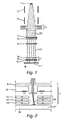
- FIG. 7 schematically shows a side view of a portion of an electrostatic lens array according to the invention, which combines different aspects.
- the insulating structure comprises portions forming a gap 78 as discussed with reference to FIG. 5 , and a surface of the insulating structure facing the first conductive plate 71 is provided with a conductive layer 76.
- An insulating structure as discussed with reference to FIG. 4 may be manufactured as follows. First, a first insulating plate is provided. In the first insulating plate, at least one first through hole is manufactured. The first through hole has a first diameter. Then, a second insulating plate is provided. In the second insulating plate at least one second through hole is manufactured, with a second diameter larger than the first diameter. Finally, the first insulating plate and the second insulating plate are combined to form an insulating structure with the apertures aligned such that the insulating structure has at least one aperture formed by the first and second through holes.
- the second insulating plate may be of a different material than the first insulating plate.
- the second insulating plate may be of the same material as the first insulating plate.
- the insulating plates being of the same material has the advantage that discontinuities in electrical and other properties at the boundary surface between the first and second insulating plates will be minimized.
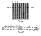
- FIG. 8A schematically shows a top view of an electrostatic lens array according to an embodiment of the invention.
- FIG. 8B schematically shows a side view of a portion of the electrostatic lens array of FIG. 8A .
- an insulating structure 97 arranged between a first conductive plate 91 provided with a plurality of first apertures 93 and a second conductive plate 92 provided with a plurality of second apertures 94 takes the form of a plurality of elongate bars or struts. The bars are arranged such that multiple openings formed by the plurality of first apertures 93 and the plurality of second apertures 94 are present between successive bars.
- the bars are represented by the black areas 83.
- Areas 81,82 correspond with areas provided with openings.
- area 82 in FIG. 8a represented by the widely spaced dashed areas, is provided with openings that are not used for providing a path for a charged particle beam.
- area 81 in FIG. 8B represented by the densely dashed areas, provides openings that serve the purpose of providing a path for a charged particle beam.
- the openings in area 82 are present to prevent side and/or edge effects. Due to the presence of the openings in area 82, the openings in area 81 experience a substantially identical electrical environment.
- FIG. 8B shows an embodiment in which edges of first apertures 93 in the first conductive plate 91 are rounded, a gap 98 is provided between a portion of the insulating structure 97 and the second conductive plate 92, and the insulating structure 97 is provided with a conductive layer 96 at a surface facing the first conductive plate 91.
Landscapes
- Chemical & Material Sciences (AREA)
- Engineering & Computer Science (AREA)
- Analytical Chemistry (AREA)
- Nanotechnology (AREA)
- Crystallography & Structural Chemistry (AREA)
- Physics & Mathematics (AREA)
- Mathematical Physics (AREA)
- Theoretical Computer Science (AREA)
- Manufacturing & Machinery (AREA)
- General Physics & Mathematics (AREA)
- Condensed Matter Physics & Semiconductors (AREA)
- Electron Beam Exposure (AREA)
- Shutters For Cameras (AREA)
Claims (16)
- Lentille électrostatique (10) comprenant :une première plaque conductrice (91) pourvue d'une première ouverture (93) ;une deuxième plaque conductrice (92) pourvue d'une deuxième ouverture (94), la deuxième ouverture (94) étant sensiblement alignée avec la première ouverture (93) ;une alimentation en tension pour fournir, pendant le fonctionnement, une première tension à la première plaque conductrice (91) et une deuxième tension à la deuxième plaque conductrice (92), la deuxième tension étant supérieure à la première tension ; etune structure isolante (97) pour séparer la première plaque conductrice (91) de la deuxième plaque conductrice (92) ;dans laquelle la structure isolante (97) comprend une première partie en contact avec la première plaque conductrice (91) et une deuxième partie en contact avec la deuxième plaque conductrice (92), la deuxième partie étant plus petite que la première partie de sorte que la première partie comprend une partie surplombante en contact avec la première plaque conductrice (91) et un espace (98) est formé entre la partie surplombante et la deuxième plaque conductrice (92), l'espace (98) étant situé du côté de la structure isolante (97) le plus proche de la deuxième ouverture (94) ; caractérisée en ce qu'une surface de la structure isolante (97) faisant face à la première plaque conductrice (91) est pourvue d'une couche conductrice (96) en contact électrique avec la première plaque conductrice (91).
- Lentille électrostatique (10) selon la revendication 1, dans laquelle la permittivité de l'espace (98) est inférieure à la permittivité de la structure isolante (97).
- Lentille électrostatique (10) selon la revendication 2, dans laquelle la permittivité de l'espace (98) est au moins quatre fois plus faible que la permittivité de la structure isolante (97).
- Lentille électrostatique (10) selon l'une quelconque des revendications précédentes, dans laquelle, en fonctionnement, l'intensité du champ électrique dans l'espace (98) entre la partie surplombante de la structure isolante (97) et la deuxième plaque conductrice (92) est supérieure à l'intensité du champ électrique à travers la deuxième partie de la structure isolante (97).
- Lentille électrostatique (10) selon l'une quelconque des revendications précédentes, dans laquelle la première partie et la deuxième partie de la structure isolante (97) ont la même épaisseur.
- Lentille électrostatique (10) selon l'une quelconque des revendications précédentes, dans laquelle la première partie et la deuxième partie de la structure isolante (97) comprennent des structures séparées qui sont liées les unes aux autres.
- Lentille électrostatique (10) selon l'une quelconque des revendications précédentes, dans laquelle la couche conductrice (96) est déposée sur une surface de la structure isolante (97) en utilisant une technique de dépôt.
- Lentille électrostatique (10) selon l'une quelconque des revendications précédentes, dans laquelle ladite couche conductrice (96) comprend du chrome ou du tantale.
- Lentille électrostatique (10) selon l'une quelconque des revendications précédentes, dans laquelle une distance entre la première plaque conductrice (91) et la deuxième plaque conductrice (92) se trouve dans une plage d'environ 100 à environ 200 µm.
- Lentille électrostatique (10) selon l'une quelconque des revendications précédentes, dans laquelle la lentille (10) est capable de résister à une intensité de champ supérieure à 10 V/µm sans décharge disruptive, et plus préférablement dans une plage de 25 à 50 V/µm sans décharge disruptive.
- Réseau de lentilles électrostatiques comprenant une pluralité de lentilles électrostatiques (10) selon l'une quelconque des revendications précédentes.
- Réseau de lentilles électrostatiques selon la revendication 11, dans lequel la structure isolante (97) prend la forme d'une plaque isolante pourvue d'au moins une troisième ouverture, ladite au moins une troisième ouverture étant agencée de sorte qu'une projection de ses parois latérales circonscrive de multiples premières ouvertures (93) et de multiples deuxièmes ouvertures (94).
- Réseau de lentilles électrostatiques selon la revendication 11, dans lequel la structure isolante (97) prend la forme d'une pluralité de barres allongées, de sorte que, entre les barres successives, de multiples trajets de transmission formés par des premières ouvertures et des deuxièmes ouvertures soient présents.
- Réseau de lentilles électrostatiques selon la revendication 11, dans lequel la structure isolante (97) prend la forme d'une pluralité de barres ou de montants allongés.
- Réseau de lentilles électrostatiques selon la revendication 14, dans lequel les barres ou les montants sont agencés de sorte que les multiples ouvertures formées par la pluralité de premières ouvertures (93) de la première plaque conductrice (91) et la pluralité de deuxièmes ouvertures (94) de la deuxième plaque conductrice (92) soient présentes entre les barres ou les montants successifs.
- Système de lithographie par petits faisceaux de particules chargées comprenant :une source (1) de particules chargées pour produire un faisceau (20) de particules chargées ;un réseau d'ouvertures (4) pour produire une pluralité de petits faisceaux (21) à partir du faisceau de particules chargées (20) ;un système de conditionnement de petits faisceaux pour conditionner la pluralité de petits faisceaux (21) selon un motif ; etle réseau de lentilles électrostatiques selon l'une quelconque des revendications 11 à 15 pour focaliser la pluralité de petits faisceaux (21).
Applications Claiming Priority (2)
| Application Number | Priority Date | Filing Date | Title |
|---|---|---|---|
| US10168208P | 2008-10-01 | 2008-10-01 | |
| PCT/EP2009/062788 WO2010037832A2 (fr) | 2008-10-01 | 2009-10-01 | Structure de lentille électrostatique |
Publications (2)
| Publication Number | Publication Date |
|---|---|
| EP2406810A2 EP2406810A2 (fr) | 2012-01-18 |
| EP2406810B1 true EP2406810B1 (fr) | 2014-09-17 |
Family
ID=41466906
Family Applications (1)
| Application Number | Title | Priority Date | Filing Date |
|---|---|---|---|
| EP09783661.3A Active EP2406810B1 (fr) | 2008-10-01 | 2009-10-01 | Structure de lentille électrostatique |
Country Status (7)
| Country | Link |
|---|---|
| US (3) | US8198602B2 (fr) |
| EP (1) | EP2406810B1 (fr) |
| JP (1) | JP5420670B2 (fr) |
| KR (1) | KR101649106B1 (fr) |
| CN (1) | CN102232237B (fr) |
| TW (1) | TWI479530B (fr) |
| WO (1) | WO2010037832A2 (fr) |
Families Citing this family (33)
| Publication number | Priority date | Publication date | Assignee | Title |
|---|---|---|---|---|
| CN102232237B (zh) * | 2008-10-01 | 2014-09-24 | 迈普尔平版印刷Ip有限公司 | 静电透镜构件 |
| CN102460633B (zh) | 2009-05-20 | 2014-12-17 | 迈普尔平版印刷Ip有限公司 | 用于光刻系统的图案数据转换器 |
| EP3144955A1 (fr) | 2009-05-20 | 2017-03-22 | Mapper Lithography IP B.V. | Procédé d'exposition d'une plaquette |
| JP2012033297A (ja) * | 2010-07-29 | 2012-02-16 | Hitachi High-Technologies Corp | 電子銃 |
| WO2012062854A1 (fr) | 2010-11-13 | 2012-05-18 | Mapper Lithography Ip B.V. | Système de lithographie et procédé de réfraction |
| US8884255B2 (en) | 2010-11-13 | 2014-11-11 | Mapper Lithography Ip B.V. | Data path for lithography apparatus |
| US9305747B2 (en) | 2010-11-13 | 2016-04-05 | Mapper Lithography Ip B.V. | Data path for lithography apparatus |
| JP5669636B2 (ja) * | 2011-03-15 | 2015-02-12 | キヤノン株式会社 | 荷電粒子線レンズおよびそれを用いた露光装置 |
| JP2012195096A (ja) * | 2011-03-15 | 2012-10-11 | Canon Inc | 荷電粒子線レンズおよびそれを用いた露光装置 |
| EP2700081B1 (fr) | 2011-04-22 | 2022-11-02 | ASML Netherlands B.V. | Architecture de réseau et protocole pour un cluster des appareils lithographiques |
| NL2007604C2 (en) * | 2011-10-14 | 2013-05-01 | Mapper Lithography Ip Bv | Charged particle system comprising a manipulator device for manipulation of one or more charged particle beams. |
| TWI514089B (zh) | 2011-04-28 | 2015-12-21 | Mapper Lithography Ip Bv | 在微影系統中用於轉移基板的設備 |
| NL2006868C2 (en) * | 2011-05-30 | 2012-12-03 | Mapper Lithography Ip Bv | Charged particle multi-beamlet apparatus. |
| WO2013045643A2 (fr) | 2011-09-28 | 2013-04-04 | Mapper Lithography Ip B.V. | Générateur de plasma |
| JP2013168396A (ja) * | 2012-02-14 | 2013-08-29 | Canon Inc | 静電型の荷電粒子線レンズ及び荷電粒子線装置 |
| WO2013142068A1 (fr) * | 2012-03-19 | 2013-09-26 | Kla-Tencor Corporation | Matrice de microlentilles électroniques supportée par des piliers |
| TW201401330A (zh) | 2012-05-14 | 2014-01-01 | Mapper Lithography Ip Bv | 帶電粒子微影系統和射束產生器 |
| US11348756B2 (en) | 2012-05-14 | 2022-05-31 | Asml Netherlands B.V. | Aberration correction in charged particle system |
| US10586625B2 (en) | 2012-05-14 | 2020-03-10 | Asml Netherlands B.V. | Vacuum chamber arrangement for charged particle beam generator |
| JP2014063866A (ja) * | 2012-09-21 | 2014-04-10 | Canon Inc | シリコン基板の加工方法及び荷電粒子線レンズの製造方法 |
| US8890092B2 (en) * | 2013-01-28 | 2014-11-18 | Industry—University Cooperation Foundation Sunmoon University | Multi-particle beam column having an electrode layer including an eccentric aperture |
| WO2015024956A1 (fr) | 2013-08-23 | 2015-02-26 | Mapper Lithography Ip B.V. | Dispositif de séchage destiné à être utilisé dans un système de lithographie |
| WO2016076722A2 (fr) | 2014-11-14 | 2016-05-19 | Mapper Lithography Ip B.V. | Système de verrouillage de charge et procédé de transfert de substrats dans un système de lithographie |
| US9691588B2 (en) | 2015-03-10 | 2017-06-27 | Hermes Microvision, Inc. | Apparatus of plural charged-particle beams |
| US10096450B2 (en) | 2015-12-28 | 2018-10-09 | Mapper Lithography Ip B.V. | Control system and method for lithography apparatus |
| EP3268979A4 (fr) * | 2016-04-13 | 2019-05-08 | Hermes Microvision Inc. | Appareil ayant plusieurs faisceaux de particules chargées |
| JP7232935B2 (ja) * | 2019-04-10 | 2023-03-03 | エーエスエムエル ネザーランズ ビー.ブイ. | 粒子ビーム装置に適したステージ装置 |
| EP4020517A1 (fr) * | 2020-12-23 | 2022-06-29 | ASML Netherlands B.V. | Dispositif optique à électrons |
| JP2024501655A (ja) * | 2020-12-23 | 2024-01-15 | エーエスエムエル ネザーランズ ビー.ブイ. | 電子レンズ |
| IL303983A (en) * | 2020-12-23 | 2023-08-01 | Asml Netherlands Bv | Charged particle optical device |
| EP4020516A1 (fr) | 2020-12-23 | 2022-06-29 | ASML Netherlands B.V. | Dispositif optique à particules chargées, ensemble lentilles d'objectif, détecteur, réseau de détecteurs et procédés |
| EP4092712A1 (fr) | 2021-05-18 | 2022-11-23 | ASML Netherlands B.V. | Dispositif optique à particules chargées et méthode utilisant un tel dispositif |
| IL310510A (en) * | 2021-08-08 | 2024-03-01 | Viamems Tech Inc | Electrostatic devices for effecting electroless particle beams |
Citations (1)
| Publication number | Priority date | Publication date | Assignee | Title |
|---|---|---|---|---|
| EP1505629A2 (fr) * | 2003-08-06 | 2005-02-09 | Canon Kabushiki Kaisha | Lentille à apertures multiples pour faisceaux de particules chargées et appareil utilisant une telle lentille |
Family Cites Families (24)
| Publication number | Priority date | Publication date | Assignee | Title |
|---|---|---|---|---|
| US4207656A (en) * | 1976-01-16 | 1980-06-17 | U.S. Philips Corporation | Color television display tube and method of manufacturing same |
| US4196373A (en) | 1978-04-10 | 1980-04-01 | General Electric Company | Electron optics apparatus |
| US4200794A (en) | 1978-11-08 | 1980-04-29 | Control Data Corporation | Micro lens array and micro deflector assembly for fly's eye electron beam tubes using silicon components and techniques of fabrication and assembly |
| JPS59211945A (ja) * | 1983-05-18 | 1984-11-30 | Hitachi Ltd | カラ−受像管用電子銃 |
| JPS63170818A (ja) * | 1987-01-09 | 1988-07-14 | 富士電機株式会社 | 直流高電圧用樹脂モ−ルド絶縁体 |
| JPS63278318A (ja) * | 1987-05-11 | 1988-11-16 | Matsushita Electric Ind Co Ltd | 電極支持体 |
| TW253971B (en) * | 1994-02-21 | 1995-08-11 | Futaba Denshi Kogyo Kk | Method for driving electron gun and cathode ray tube |
| JPH1040844A (ja) * | 1996-07-26 | 1998-02-13 | Shinko Pantec Co Ltd | 高耐圧無放電対電極 |
| JP3103800B2 (ja) | 1999-03-11 | 2000-10-30 | 科学技術振興事業団 | 高電圧絶縁部材 |
| JP3763446B2 (ja) * | 1999-10-18 | 2006-04-05 | キヤノン株式会社 | 静電レンズ、電子ビーム描画装置、荷電ビーム応用装置、および、デバイス製造方法 |
| JP4036417B2 (ja) * | 2000-02-03 | 2008-01-23 | キヤノン株式会社 | 画像形成装置 |
| JP2001283756A (ja) * | 2000-03-31 | 2001-10-12 | Canon Inc | 電子光学系アレイ、これを用いた荷電粒子線露光装置ならびにデバイス製造方法 |
| JP2002134051A (ja) * | 2000-10-20 | 2002-05-10 | Seiko Instruments Inc | 電磁界重畳型レンズ及びこれを用いた電子線装置 |
| EP2434522B8 (fr) * | 2002-07-16 | 2014-07-23 | Canon Kabushiki Kaisha | Lentille à faisceaux multiples de particules chargées, appareil d'exposition aux faisceaux de particules chargées utilisant la même lentille, et la méthode correspondante de fabrication. |
| EP2579273B8 (fr) * | 2003-09-05 | 2019-05-22 | Carl Zeiss Microscopy GmbH | Systemes et dispositifs d'optique particulaire et composants d'optique particulaire pour de tels systemes et dispositifs |
| KR100496643B1 (ko) * | 2003-10-25 | 2005-06-20 | 한국전자통신연구원 | 마이크로칼럼 전자빔 장치의 자체정렬 적층 금속 박막전자빔 렌즈 및 그 제작방법 |
| JP4124131B2 (ja) * | 2004-02-02 | 2008-07-23 | 株式会社Nhvコーポレーション | 電子線加速器用加速管 |
| US7045794B1 (en) | 2004-06-18 | 2006-05-16 | Novelx, Inc. | Stacked lens structure and method of use thereof for preventing electrical breakdown |
| TWI415162B (zh) * | 2005-03-03 | 2013-11-11 | Toshiba Kk | 映像投影型電子線裝置及使用該裝置之缺陷檢查系統 |
| JP2007173069A (ja) * | 2005-12-22 | 2007-07-05 | Japan Atomic Energy Agency | 超低エネルギーイオン源用電極 |
| US8134135B2 (en) * | 2006-07-25 | 2012-03-13 | Mapper Lithography Ip B.V. | Multiple beam charged particle optical system |
| KR20090052350A (ko) | 2006-09-11 | 2009-05-25 | 전자빔기술센터 주식회사 | 전자 칼럼용 렌즈 조립체 |
| US7576337B2 (en) | 2007-01-05 | 2009-08-18 | Varian Semiconductor Equipment Associates, Inc. | Power supply for an ion implantation system |
| CN102232237B (zh) * | 2008-10-01 | 2014-09-24 | 迈普尔平版印刷Ip有限公司 | 静电透镜构件 |
-
2009
- 2009-10-01 CN CN200980148233.3A patent/CN102232237B/zh active Active
- 2009-10-01 TW TW098133357A patent/TWI479530B/zh active
- 2009-10-01 EP EP09783661.3A patent/EP2406810B1/fr active Active
- 2009-10-01 KR KR1020117009983A patent/KR101649106B1/ko active IP Right Grant
- 2009-10-01 WO PCT/EP2009/062788 patent/WO2010037832A2/fr active Application Filing
- 2009-10-01 JP JP2011529560A patent/JP5420670B2/ja active Active
-
2011
- 2011-03-31 US US13/076,540 patent/US8198602B2/en not_active Ceased
-
2014
- 2014-06-12 US US14/302,522 patent/USRE46452E1/en active Active
-
2017
- 2017-06-26 US US15/632,477 patent/US20170309438A1/en not_active Abandoned
Patent Citations (1)
| Publication number | Priority date | Publication date | Assignee | Title |
|---|---|---|---|---|
| EP1505629A2 (fr) * | 2003-08-06 | 2005-02-09 | Canon Kabushiki Kaisha | Lentille à apertures multiples pour faisceaux de particules chargées et appareil utilisant une telle lentille |
Also Published As
| Publication number | Publication date |
|---|---|
| US20170309438A1 (en) | 2017-10-26 |
| KR101649106B1 (ko) | 2016-08-19 |
| TWI479530B (zh) | 2015-04-01 |
| EP2406810A2 (fr) | 2012-01-18 |
| KR20110081253A (ko) | 2011-07-13 |
| WO2010037832A3 (fr) | 2010-06-10 |
| USRE46452E1 (en) | 2017-06-27 |
| WO2010037832A4 (fr) | 2010-08-12 |
| CN102232237B (zh) | 2014-09-24 |
| CN102232237A (zh) | 2011-11-02 |
| TW201032258A (en) | 2010-09-01 |
| US8198602B2 (en) | 2012-06-12 |
| JP2012504843A (ja) | 2012-02-23 |
| JP5420670B2 (ja) | 2014-02-19 |
| WO2010037832A2 (fr) | 2010-04-08 |
| US20110216299A1 (en) | 2011-09-08 |
Similar Documents
| Publication | Publication Date | Title |
|---|---|---|
| EP2406810B1 (fr) | Structure de lentille électrostatique | |
| EP2260499B1 (fr) | Configuration de lentilles de projection | |
| KR101481950B1 (ko) | 투사 렌즈 배열체 | |
| US8618496B2 (en) | Charged particle system comprising a manipulator device for manipulation of one or more charged particle beams | |
| TWI691998B (zh) | 靜電多極元件、靜電多極裝置及製造靜電多極元件的方法 | |
| US8502176B2 (en) | Imaging system | |
| JP2023517626A (ja) | マルチビーム発生ユニットおよびマルチビーム偏向ユニットの特定の改善 | |
| JP4541798B2 (ja) | 荷電粒子線レンズアレイ、及び該荷電粒子線レンズアレイを用いた荷電粒子線露光装置 | |
| JP2006049703A (ja) | 荷電粒子線レンズアレイ、及び該荷電粒子線レンズアレイを用いた荷電粒子線露光装置 | |
| JP4402077B2 (ja) | 荷電粒子線レンズアレイ、露光装置及びデバイス製造方法 | |
| JP2013030567A (ja) | 荷電粒子線レンズアレイ |
Legal Events
| Date | Code | Title | Description |
|---|---|---|---|
| PUAI | Public reference made under article 153(3) epc to a published international application that has entered the european phase |
Free format text: ORIGINAL CODE: 0009012 |
|
| 17P | Request for examination filed |
Effective date: 20110429 |
|
| AK | Designated contracting states |
Kind code of ref document: A2 Designated state(s): AT BE BG CH CY CZ DE DK EE ES FI FR GB GR HR HU IE IS IT LI LT LU LV MC MK MT NL NO PL PT RO SE SI SK SM TR |
|
| RIN1 | Information on inventor provided before grant (corrected) |
Inventor name: STEENBRINK, STIJN WILLEM HERMAN KAREL Inventor name: VELTMAN, PETER Inventor name: KONING, JOHAN JOOST |
|
| 17Q | First examination report despatched |
Effective date: 20120309 |
|
| GRAP | Despatch of communication of intention to grant a patent |
Free format text: ORIGINAL CODE: EPIDOSNIGR1 |
|
| RIC1 | Information provided on ipc code assigned before grant |
Ipc: B82Y 10/00 20110101ALI20130723BHEP Ipc: H01J 37/04 20060101AFI20130723BHEP Ipc: H01J 37/317 20060101ALI20130723BHEP Ipc: B82Y 40/00 20110101ALI20130723BHEP Ipc: H01J 37/12 20060101ALI20130723BHEP |
|
| INTG | Intention to grant announced |
Effective date: 20130827 |
|
| GRAP | Despatch of communication of intention to grant a patent |
Free format text: ORIGINAL CODE: EPIDOSNIGR1 |
|
| INTG | Intention to grant announced |
Effective date: 20140403 |
|
| INTG | Intention to grant announced |
Effective date: 20140409 |
|
| GRAS | Grant fee paid |
Free format text: ORIGINAL CODE: EPIDOSNIGR3 |
|
| GRAA | (expected) grant |
Free format text: ORIGINAL CODE: 0009210 |
|
| AK | Designated contracting states |
Kind code of ref document: B1 Designated state(s): AT BE BG CH CY CZ DE DK EE ES FI FR GB GR HR HU IE IS IT LI LT LU LV MC MK MT NL NO PL PT RO SE SI SK SM TR |
|
| REG | Reference to a national code |
Ref country code: GB Ref legal event code: FG4D |
|
| REG | Reference to a national code |
Ref country code: CH Ref legal event code: EP |
|
| REG | Reference to a national code |
Ref country code: IE Ref legal event code: FG4D |
|
| REG | Reference to a national code |
Ref country code: AT Ref legal event code: REF Ref document number: 688022 Country of ref document: AT Kind code of ref document: T Effective date: 20141015 |
|
| REG | Reference to a national code |
Ref country code: DE Ref legal event code: R096 Ref document number: 602009026753 Country of ref document: DE Effective date: 20141030 |
|
| REG | Reference to a national code |
Ref country code: NL Ref legal event code: T3 |
|
| PG25 | Lapsed in a contracting state [announced via postgrant information from national office to epo] |
Ref country code: SE Free format text: LAPSE BECAUSE OF FAILURE TO SUBMIT A TRANSLATION OF THE DESCRIPTION OR TO PAY THE FEE WITHIN THE PRESCRIBED TIME-LIMIT Effective date: 20140917 Ref country code: GR Free format text: LAPSE BECAUSE OF FAILURE TO SUBMIT A TRANSLATION OF THE DESCRIPTION OR TO PAY THE FEE WITHIN THE PRESCRIBED TIME-LIMIT Effective date: 20141218 Ref country code: FI Free format text: LAPSE BECAUSE OF FAILURE TO SUBMIT A TRANSLATION OF THE DESCRIPTION OR TO PAY THE FEE WITHIN THE PRESCRIBED TIME-LIMIT Effective date: 20140917 Ref country code: NO Free format text: LAPSE BECAUSE OF FAILURE TO SUBMIT A TRANSLATION OF THE DESCRIPTION OR TO PAY THE FEE WITHIN THE PRESCRIBED TIME-LIMIT Effective date: 20141217 Ref country code: LT Free format text: LAPSE BECAUSE OF FAILURE TO SUBMIT A TRANSLATION OF THE DESCRIPTION OR TO PAY THE FEE WITHIN THE PRESCRIBED TIME-LIMIT Effective date: 20140917 |
|
| REG | Reference to a national code |
Ref country code: LT Ref legal event code: MG4D |
|
| PG25 | Lapsed in a contracting state [announced via postgrant information from national office to epo] |
Ref country code: HR Free format text: LAPSE BECAUSE OF FAILURE TO SUBMIT A TRANSLATION OF THE DESCRIPTION OR TO PAY THE FEE WITHIN THE PRESCRIBED TIME-LIMIT Effective date: 20140917 Ref country code: LV Free format text: LAPSE BECAUSE OF FAILURE TO SUBMIT A TRANSLATION OF THE DESCRIPTION OR TO PAY THE FEE WITHIN THE PRESCRIBED TIME-LIMIT Effective date: 20140917 Ref country code: CY Free format text: LAPSE BECAUSE OF FAILURE TO SUBMIT A TRANSLATION OF THE DESCRIPTION OR TO PAY THE FEE WITHIN THE PRESCRIBED TIME-LIMIT Effective date: 20140917 |
|
| PG25 | Lapsed in a contracting state [announced via postgrant information from national office to epo] |
Ref country code: PT Free format text: LAPSE BECAUSE OF FAILURE TO SUBMIT A TRANSLATION OF THE DESCRIPTION OR TO PAY THE FEE WITHIN THE PRESCRIBED TIME-LIMIT Effective date: 20150119 Ref country code: IS Free format text: LAPSE BECAUSE OF FAILURE TO SUBMIT A TRANSLATION OF THE DESCRIPTION OR TO PAY THE FEE WITHIN THE PRESCRIBED TIME-LIMIT Effective date: 20150117 Ref country code: RO Free format text: LAPSE BECAUSE OF FAILURE TO SUBMIT A TRANSLATION OF THE DESCRIPTION OR TO PAY THE FEE WITHIN THE PRESCRIBED TIME-LIMIT Effective date: 20140917 Ref country code: ES Free format text: LAPSE BECAUSE OF FAILURE TO SUBMIT A TRANSLATION OF THE DESCRIPTION OR TO PAY THE FEE WITHIN THE PRESCRIBED TIME-LIMIT Effective date: 20140917 Ref country code: SK Free format text: LAPSE BECAUSE OF FAILURE TO SUBMIT A TRANSLATION OF THE DESCRIPTION OR TO PAY THE FEE WITHIN THE PRESCRIBED TIME-LIMIT Effective date: 20140917 Ref country code: CZ Free format text: LAPSE BECAUSE OF FAILURE TO SUBMIT A TRANSLATION OF THE DESCRIPTION OR TO PAY THE FEE WITHIN THE PRESCRIBED TIME-LIMIT Effective date: 20140917 Ref country code: EE Free format text: LAPSE BECAUSE OF FAILURE TO SUBMIT A TRANSLATION OF THE DESCRIPTION OR TO PAY THE FEE WITHIN THE PRESCRIBED TIME-LIMIT Effective date: 20140917 |
|
| PG25 | Lapsed in a contracting state [announced via postgrant information from national office to epo] |
Ref country code: PL Free format text: LAPSE BECAUSE OF FAILURE TO SUBMIT A TRANSLATION OF THE DESCRIPTION OR TO PAY THE FEE WITHIN THE PRESCRIBED TIME-LIMIT Effective date: 20140917 |
|
| REG | Reference to a national code |
Ref country code: CH Ref legal event code: PL |
|
| REG | Reference to a national code |
Ref country code: DE Ref legal event code: R097 Ref document number: 602009026753 Country of ref document: DE |
|
| PG25 | Lapsed in a contracting state [announced via postgrant information from national office to epo] |
Ref country code: BE Free format text: LAPSE BECAUSE OF NON-PAYMENT OF DUE FEES Effective date: 20141031 Ref country code: MC Free format text: LAPSE BECAUSE OF FAILURE TO SUBMIT A TRANSLATION OF THE DESCRIPTION OR TO PAY THE FEE WITHIN THE PRESCRIBED TIME-LIMIT Effective date: 20140917 |
|
| PLBE | No opposition filed within time limit |
Free format text: ORIGINAL CODE: 0009261 |
|
| STAA | Information on the status of an ep patent application or granted ep patent |
Free format text: STATUS: NO OPPOSITION FILED WITHIN TIME LIMIT |
|
| PG25 | Lapsed in a contracting state [announced via postgrant information from national office to epo] |
Ref country code: DK Free format text: LAPSE BECAUSE OF FAILURE TO SUBMIT A TRANSLATION OF THE DESCRIPTION OR TO PAY THE FEE WITHIN THE PRESCRIBED TIME-LIMIT Effective date: 20140917 Ref country code: CH Free format text: LAPSE BECAUSE OF NON-PAYMENT OF DUE FEES Effective date: 20141031 Ref country code: LI Free format text: LAPSE BECAUSE OF NON-PAYMENT OF DUE FEES Effective date: 20141031 |
|
| 26N | No opposition filed |
Effective date: 20150618 |
|
| PG25 | Lapsed in a contracting state [announced via postgrant information from national office to epo] |
Ref country code: IT Free format text: LAPSE BECAUSE OF FAILURE TO SUBMIT A TRANSLATION OF THE DESCRIPTION OR TO PAY THE FEE WITHIN THE PRESCRIBED TIME-LIMIT Effective date: 20140917 |
|
| REG | Reference to a national code |
Ref country code: FR Ref legal event code: PLFP Year of fee payment: 7 |
|
| PG25 | Lapsed in a contracting state [announced via postgrant information from national office to epo] |
Ref country code: SI Free format text: LAPSE BECAUSE OF FAILURE TO SUBMIT A TRANSLATION OF THE DESCRIPTION OR TO PAY THE FEE WITHIN THE PRESCRIBED TIME-LIMIT Effective date: 20140917 |
|
| PG25 | Lapsed in a contracting state [announced via postgrant information from national office to epo] |
Ref country code: SM Free format text: LAPSE BECAUSE OF FAILURE TO SUBMIT A TRANSLATION OF THE DESCRIPTION OR TO PAY THE FEE WITHIN THE PRESCRIBED TIME-LIMIT Effective date: 20140917 |
|
| PG25 | Lapsed in a contracting state [announced via postgrant information from national office to epo] |
Ref country code: BG Free format text: LAPSE BECAUSE OF FAILURE TO SUBMIT A TRANSLATION OF THE DESCRIPTION OR TO PAY THE FEE WITHIN THE PRESCRIBED TIME-LIMIT Effective date: 20140917 |
|
| PG25 | Lapsed in a contracting state [announced via postgrant information from national office to epo] |
Ref country code: LU Free format text: LAPSE BECAUSE OF NON-PAYMENT OF DUE FEES Effective date: 20141001 Ref country code: TR Free format text: LAPSE BECAUSE OF FAILURE TO SUBMIT A TRANSLATION OF THE DESCRIPTION OR TO PAY THE FEE WITHIN THE PRESCRIBED TIME-LIMIT Effective date: 20140917 Ref country code: MT Free format text: LAPSE BECAUSE OF FAILURE TO SUBMIT A TRANSLATION OF THE DESCRIPTION OR TO PAY THE FEE WITHIN THE PRESCRIBED TIME-LIMIT Effective date: 20140917 Ref country code: HU Free format text: LAPSE BECAUSE OF FAILURE TO SUBMIT A TRANSLATION OF THE DESCRIPTION OR TO PAY THE FEE WITHIN THE PRESCRIBED TIME-LIMIT; INVALID AB INITIO Effective date: 20091001 |
|
| REG | Reference to a national code |
Ref country code: FR Ref legal event code: PLFP Year of fee payment: 8 |
|
| REG | Reference to a national code |
Ref country code: FR Ref legal event code: PLFP Year of fee payment: 9 |
|
| PG25 | Lapsed in a contracting state [announced via postgrant information from national office to epo] |
Ref country code: MK Free format text: LAPSE BECAUSE OF FAILURE TO SUBMIT A TRANSLATION OF THE DESCRIPTION OR TO PAY THE FEE WITHIN THE PRESCRIBED TIME-LIMIT Effective date: 20140917 |
|
| REG | Reference to a national code |
Ref country code: FR Ref legal event code: PLFP Year of fee payment: 10 |
|
| REG | Reference to a national code |
Ref country code: NL Ref legal event code: PD Owner name: ASML NETHERLANDS B.V.; NL Free format text: DETAILS ASSIGNMENT: CHANGE OF OWNER(S), ASSIGNMENT; FORMER OWNER NAME: MAPPER LITHOGRAPHY IP B.V. Effective date: 20190425 |
|
| PGFP | Annual fee paid to national office [announced via postgrant information from national office to epo] |
Ref country code: GB Payment date: 20221018 Year of fee payment: 14 |
|
| P01 | Opt-out of the competence of the unified patent court (upc) registered |
Effective date: 20230403 |
|
| PGFP | Annual fee paid to national office [announced via postgrant information from national office to epo] |
Ref country code: NL Payment date: 20231026 Year of fee payment: 15 |
|
| PGFP | Annual fee paid to national office [announced via postgrant information from national office to epo] |
Ref country code: IE Payment date: 20231018 Year of fee payment: 15 Ref country code: FR Payment date: 20231026 Year of fee payment: 15 Ref country code: DE Payment date: 20231027 Year of fee payment: 15 Ref country code: AT Payment date: 20231018 Year of fee payment: 15 |