EP2405575B1 - Unmittelbare Aktualisatierung von Pulsbreitmodulationswerten - Google Patents
Unmittelbare Aktualisatierung von Pulsbreitmodulationswerten Download PDFInfo
- Publication number
- EP2405575B1 EP2405575B1 EP11184051.8A EP11184051A EP2405575B1 EP 2405575 B1 EP2405575 B1 EP 2405575B1 EP 11184051 A EP11184051 A EP 11184051A EP 2405575 B1 EP2405575 B1 EP 2405575B1
- Authority
- EP
- European Patent Office
- Prior art keywords
- duty cycle
- pwm
- period
- register
- counter
- Prior art date
- Legal status (The legal status is an assumption and is not a legal conclusion. Google has not performed a legal analysis and makes no representation as to the accuracy of the status listed.)
- Active
Links
Images


Classifications
-
- H—ELECTRICITY
- H03—ELECTRONIC CIRCUITRY
- H03K—PULSE TECHNIQUE
- H03K7/00—Modulating pulses with a continuously-variable modulating signal
- H03K7/08—Duration or width modulation ; Duty cycle modulation
-
- H—ELECTRICITY
- H03—ELECTRONIC CIRCUITRY
- H03K—PULSE TECHNIQUE
- H03K7/00—Modulating pulses with a continuously-variable modulating signal
Definitions
- the present disclosure relates to digital devices having digital pulse width modulation (PWM) capabilities, and more particularly, to a digital device allowing immediate update of changes in PWM duty cycle and/or period values.
- PWM pulse width modulation
- a typical conventional pulse width modulation circuit is known from WO 2006/023427 , for example as shown in Fig. 11.
- SMPS Switch Mode Power Supplies
- the ability to provide immediate (asynchronous) update of PWM duty cycle values is very important in Switch Mode Power Supplies (SMPS) because the control loop stability and performance is inversely proportional to the control loop "lag.”
- the "lag" is the time from the acquisition of the feedback information until new stimulus is provided to the system.
- Present technology PWM generators may incur a delay from the calculation of new stimulus value (duty cycle or period) till the PWM can be updated at the next PWM boundary (synchronous update). This delay may be caused (1) if a new smaller duty cycle value or period value is programmed into the PWM generator, (2) if the PWM cycle counter has advanced beyond the new duty cycle or period value, and (3) if an EQUAL comparison is made between the duty cycle or period value and the PWM cycle count value.
- a PWM cycle counter may "MISS" the maximum duty cycle or period value and remain “ON” until the PWM counter reaches its hardware limitation and “rolls over” from a maximum count to a zero count, thus beginning the next PWM cycle.
- This "roll over” time may be multiples of the desired PWM cycle duration and may cause serious functional problems when controlling a SMPS.
- SMPS Switch Mode Power Supply
- an apparatus for generating pulse width modulation may comprise: a timer/counter; a period register; a duty cycle register; a first comparator having a first input coupled to the period register, a second input coupled to the timer/counter and an output coupled to a reset of the timer/counter such that a count value of the timer/counter resets when the count value is equal to or greater than a period value stored in the period register; and a second comparator having a first input coupled to the duty cycle register, a second input coupled to the timer/counter and an output generating a PWM signal, wherein the PWM signal is at a first logic level when the count value is less than a duty cycle value stored in the duty cycle register, otherwise the PWM signal at the output of the second comparator is at a second logic level.
- PWM pulse width modulation
- a method for generating pulse width modulation may comprise the steps of: providing a period value; providing a duty cycle value; incrementing a time count value; comparing the time count value with the period value such that when the time count value is equal to or greater than the period value the time count value is reset to a first time count value; and comparing the time count value with the duty cycle value such that when the time count value is less than the duty cycle value then a PWM signal is at a first logic level, otherwise the PWM signal is at a second logic level.
- a prior technology PWM generator may comprise a period register 102, a timer/counter 104, a duty cycle register 106, a timer/period comparator 108, a duty cycle update register 110, a duty cycle/timer comparator 112, and a PWM flip-flop 118.
- the period register 102 may be loaded with the desired period and the duty cycle register 106 may be loaded with the desired duty cycle for the PWM signal 114 (see Figures 3 and 5 ).
- the timer/counter 104 incrementally counts until its count value is equal to the period value stored in the period register 102.
- the PWM flip-flop 118 When both are equal, the PWM flip-flop 118 is set (Q-output goes high or logic "1"), then timer/counter 104 is reset back to zero and begins incrementally counting up again until its count and the period value are equal as determined by the comparator 108. Whenever the count value from the timer counter 104 is equal to the period value stored in the period register 102, the duty cycle update register 110 will be loaded with the desired duty cycle value stored in the duty cycle register 106.
- the duty cycle/timer comparator 112 determines when the count from the timer/counter 104 equals the PWM duty cycle value stored in the duty cycle update register 110, and when equal an output 114 from the duty cycle update register 110 clears the PWM flip-flop 118 (Q-output goes low or logic "0") thereby generating a PWM signal at output 120 of the PWM flip-flop 118.
- the comparator 112 and the flip-flop 118 are used to force duty cycle updates and PWM cycle boundaries (completed periods) to avoid potential errors in the PWM signal.
- a PWM generator may comprise a period register 102, a timer/counter 104, a duty cycle register 106, a timer/period comparator 208, and a duty cycle/timer comparator 212.
- the period register 102 may be loaded with the desired period and the duty cycle register 106 may be loaded with a desired duty cycle for the PWM signal 214 (see Figures 4 and 6 ).
- the timer/counter 104 incrementally counts until its count value is equal to or greater than the period value stored in the period register 102, then the timer/counter 104 resets back to zero and begins incrementally counting up again.
- a PWM period change may be immediately updated and not have to wait for completion of a present PWM period. This is especially important when the PWM period is shortened.
- the duty cycle/timer comparator 212 generates the PWM signal at its output 214 whenever the value from the timer/counter 104 is less than the value in the duty cycle register 106.
- This feature allows an immediate duty cycle update (asynchronous updating) to the new PWM duty cycle values instead of waiting until the end of a PWM period to accept the new duty cycle values. This reduces the latency in a control loop when responding to changing system status, e.g., changes in PWM duty cycle, and prevents PWM "run away" (e.g., missing a PWM cycle) if the PWM duty cycle timer/counter 104 has advanced beyond the updated duty-cycle maximum value.
- a duty cycle update register register 110 of Figure 1
- logic of a digital device 702 may be used to write and/or read duty cycle values to/from the duty cycle register 106, and to write and/or read period values to/from the period register 102.
- the PWM generator 200 may also be part of (integral with) the logic circuits of the digital device 702.
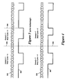
- FIG. 3 depicted is a schematic timing diagram of a PWM signal from the PWM generator illustrated in Figure 1 .
- Clock waveforms 320 generally represent the PWM generator clocks used in determining the PWM periods and duty cycles.
- FIG. 4 depicted is a schematic timing diagram of a PWM signal from the specific exemplary embodiment of the PWM generator illustrated in Figure 2 , according to the specific example embodiment of this disclosure.
- the PWM signal waveform 402 immediately assumes the new duty cycle of 5.
- FIG. 5 depicted is another schematic timing diagram of a PWM signal from the PWM generator illustrated in Figure 1 .
- the PWM duty cycle counter 106 has "MISSED" the maximum duty cycle value and remains “ON” until the counter 106 reaches its hardware limitation and "rolls over” from, e . g., FFFF to a zero count beginning at the next PWM period. This "roll over" time may be multiple desired PWM duty cycles and may cause serious functional control problems.
- a PWM duty cycle 508 was lost (indicated by dashed lines between times 504 and 506.
- FIG. 6 depicted is another schematic timing diagram of a PWM signal from the specific exemplary embodiment of the PWM generator illustrated in Figure 2 , according to the specific example embodiment of this disclosure.
- the duty cycle is changed (decreased) to 3 and the PWM signal waveform 502 assumes the new duty cycle of 3 immediately.
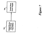
- a digital device 702 e.g., microprocessor, microcontroller, digital signal processor (DSP), programmable logic array (PLA), application specific integrated circuit (ASIC) and the like, may be coupled to a switch mode power supply 704, or any other system using PWM for control thereof.
- the duty cycle register 106 and/or the period register 102 ( Figure 2 ) may be loaded (and/or read) by the digital device 702.
Landscapes
- Dc-Dc Converters (AREA)
- Pulse Circuits (AREA)
- Feedback Control In General (AREA)
Claims (9)
- Vorrichtung zum Erzeugen von Pulsdauermodulation (PWM), die aufweist:einen Taktgeber/Zähler (104);ein Periodendauerregister (102);ein Tastverhältnisregister (106);einen ersten Komparator (108), der einen ersten mit dem Periodendauerregister (102) gekoppelten Eingang, einen zweiten mit dem Taktgeber/Zähler (104) gekoppelten Eingang und einen mit einem Reset des Taktgeber/Zähler (104) gekoppelten Ausgang (116) aufweist; undeinen zweiten Komparator, der einen ersten mit dem Tastverhältnisregister (106) gekoppelten Eingang, einen zweiten mit dem Taktgeber/Zähler (104) gekoppelten Eingang und einen Ausgang (114) aufweist, der ein PWM Signal erzeugt, wobei das PWM Signal einen ersten logischen Pegel aufweist, wenn der Zählerwert kleiner ist als ein in dem Tastverhältnisregister (106) gespeicherter Tastverhältniswert, andernfalls das PWM Signal an dem Ausgang des zweiten Komparators (114) einen zweiten logischen Pegel aufweist,dadurch gekennzeichnet, dassder erste Komparator derart eingerichtet ist, dass ein Zählerwert des Taktgeber/Zähler (104) zurückgesetzt wird, wenn der Zählerwert gleich oder größer ist als ein in dem Periodendauerregister (102) gespeicherter Periodendauerwert.
- Vorrichtung gemäß Anspruch 1, die weiterhin eine mit dem Periodendauerregister (102) und dem Tastverhältnisregister (106) gekoppelte digitale Anordnung aufweist.
- Vorrichtung gemäß Anspruch 2, wobei die digitale Anordnung ausgewählt ist aus der Gruppe die besteht aus einem Mikroprozessor, einem Mikrocontroller, einem digitalen Signalprozessor (DSP), einem Application Specific Integrated Circuit (ASIC) und einem programmierbaren Logikarray (PLA).
- Vorrichtung gemäß Anspruch 2 oder 3, wobei die digitale Anordnung betreibbar ist, um den Periodendauerwert in das Periodendauerregister (102) zu schreiben.
- Vorrichtung gemäß einem der vorherigen Ansprüche 2 bis 4, wobei die digitale Anordnung betreibbar ist, um den Tastverhältniswert in das Tastverhältnisregister (106) zu schreiben.
- Vorrichtung gemäß einem der vorherigen Ansprüche 2 bis 5, wobei die digitale Anordnung betreibbar ist, um den Periodendauerwert aus dem Periodendauerregister (102) zu lesen.
- Vorrichtung gemäß einem der vorherigen Ansprüche 2 bis 6, wobei die digitale Anordnung betreibbar ist, um den Tastverhältniswert aus dem Tastverhältnisregister (106) zu lesen.
- Vorrichtung gemäß einem der vorherigen Ansprüche, wobei der erste logische Pegel eine logische "1" ist und der zweite logische Pegel eine logische "0" ist.
- Vorrichtung gemäß einem der vorherigen Ansprüche 1 bis 7, wobei der erste logische Pegel eine logische "0" ist und der zweite logische Pegel eine logische "1" ist.
Applications Claiming Priority (3)
| Application Number | Priority Date | Filing Date | Title |
|---|---|---|---|
| US78896406P | 2006-04-04 | 2006-04-04 | |
| US11/620,499 US7646808B2 (en) | 2006-04-04 | 2007-01-05 | Allowing immediate update of pulse width modulation values |
| EP07759942A EP2005589B1 (de) | 2006-04-04 | 2007-04-02 | Unmittelbare aktualisierung von pulsbreitenmodulationswerten |
Related Parent Applications (1)
| Application Number | Title | Priority Date | Filing Date |
|---|---|---|---|
| EP07759942.1 Division | 2007-04-02 |
Publications (2)
| Publication Number | Publication Date |
|---|---|
| EP2405575A1 EP2405575A1 (de) | 2012-01-11 |
| EP2405575B1 true EP2405575B1 (de) | 2013-06-19 |
Family
ID=38556293
Family Applications (2)
| Application Number | Title | Priority Date | Filing Date |
|---|---|---|---|
| EP11184051.8A Active EP2405575B1 (de) | 2006-04-04 | 2007-04-02 | Unmittelbare Aktualisatierung von Pulsbreitmodulationswerten |
| EP07759942A Active EP2005589B1 (de) | 2006-04-04 | 2007-04-02 | Unmittelbare aktualisierung von pulsbreitenmodulationswerten |
Family Applications After (1)
| Application Number | Title | Priority Date | Filing Date |
|---|---|---|---|
| EP07759942A Active EP2005589B1 (de) | 2006-04-04 | 2007-04-02 | Unmittelbare aktualisierung von pulsbreitenmodulationswerten |
Country Status (7)
| Country | Link |
|---|---|
| US (1) | US7646808B2 (de) |
| EP (2) | EP2405575B1 (de) |
| KR (1) | KR101158531B1 (de) |
| CN (2) | CN102769448B (de) |
| AT (1) | ATE540476T1 (de) |
| TW (1) | TWI440311B (de) |
| WO (1) | WO2007115250A2 (de) |
Families Citing this family (23)
| Publication number | Priority date | Publication date | Assignee | Title |
|---|---|---|---|---|
| JP4198639B2 (ja) * | 2004-05-27 | 2008-12-17 | Necエレクトロニクス株式会社 | 割り込み発生回路 |
| US20090114526A1 (en) * | 2006-12-11 | 2009-05-07 | Huping Hu | Method and apparatus for producing non-local physical, chemical and biological effects |
| JP5319986B2 (ja) * | 2008-08-26 | 2013-10-16 | ルネサスエレクトロニクス株式会社 | パルス生成装置 |
| GB2470591A (en) * | 2009-05-29 | 2010-12-01 | Powervation Ltd | Pulse width modulation synchronisation of switched mode power converters |
| TWM380664U (en) * | 2010-01-08 | 2010-05-11 | Ta-I Liu | Digital pulse width modulating device |
| CN101820280B (zh) * | 2010-05-18 | 2011-11-23 | 中国航天科技集团公司第九研究院第七七一研究所 | 用于脉宽调制器异相驱动的检相纠相电路 |
| CN101820279B (zh) * | 2010-05-18 | 2012-05-23 | 中国航天科技集团公司第九研究院第七七一研究所 | 用于多个脉宽调制器同步的电路 |
| EP2432124B1 (de) * | 2010-09-21 | 2016-05-11 | Harman Becker Automotive Systems GmbH | Pulsweitenmodulator |
| US8432208B2 (en) * | 2011-09-28 | 2013-04-30 | Microchip Technology Incorporated | Maintaining pulse width modulation data-set coherency |
| US8362819B1 (en) | 2011-09-29 | 2013-01-29 | Microchip Technology Incorporated | Synchronizing multi-frequency pulse width modulation generators |
| US8558632B2 (en) * | 2011-09-29 | 2013-10-15 | Microchip Technology Incorporated | Repetitive single cycle pulse width modulation generation |
| US8472213B2 (en) * | 2011-09-29 | 2013-06-25 | Microchip Technology Incorporated | Extending pulse width modulation phase offset |
| FR3007906B1 (fr) * | 2013-06-27 | 2015-06-19 | Valeo Systemes Thermiques | Module de commande mli, notamment pour la commande d'un moteur electrique de climatisation |
| US9323302B2 (en) * | 2013-12-19 | 2016-04-26 | International Business Machines Corporation | Rotating voltage control |
| KR102193883B1 (ko) | 2014-10-08 | 2020-12-22 | 삼성전자주식회사 | 클럭 신호 처리기 및 이를 포함하는 비휘발성 메모리 장치 |
| TWI551053B (zh) * | 2015-01-14 | 2016-09-21 | 新唐科技股份有限公司 | 脈寬調變訊號產生電路與方法 |
| KR101768603B1 (ko) | 2017-04-25 | 2017-08-17 | 주식회사 지니틱스 | 주파수와 듀티가 변화하는 인버터 제어용 pwm 신호 발생기 |
| KR102644538B1 (ko) * | 2018-05-17 | 2024-03-06 | 현대자동차주식회사 | 모터 제어를 위한 pwm 듀티의 연산 수행을 감시하는 시스템 |
| CN111082645B (zh) * | 2020-01-19 | 2022-12-13 | 杭州禾迈电力电子技术有限公司 | 变频pwm控制开关参数更新方法、pwm控制方法及控制装置 |
| IT202100005354A1 (it) | 2021-03-08 | 2022-09-08 | Stmicroelectronics Application Gmbh | Circuito microcontrollore, dispositivo, sistema e procedimento di funzionamento corrispondenti |
| CN114443536A (zh) * | 2022-01-26 | 2022-05-06 | 西安凯锐测控科技有限公司 | 一种信号发生器变更设置参数的方法 |
| US12191760B2 (en) * | 2022-10-17 | 2025-01-07 | Texas Instruments Incorporated | Pulse width modulation circuit |
| CN118033383A (zh) * | 2024-04-11 | 2024-05-14 | 杭州芯云半导体技术有限公司 | Pwm波形的测试方法、装置及测试机 |
Family Cites Families (6)
| Publication number | Priority date | Publication date | Assignee | Title |
|---|---|---|---|---|
| US6487246B1 (en) * | 1999-04-08 | 2002-11-26 | National Semiconductor Corporation | Method and apparatus for programmable pulse width modulated signal generation with period and duty cycle values updated with controlled relative timing |
| JP3843880B2 (ja) * | 2001-05-31 | 2006-11-08 | 株式会社デンソー | ガス濃度センサのヒータ制御装置 |
| US6937084B2 (en) * | 2001-06-01 | 2005-08-30 | Microchip Technology Incorporated | Processor with dual-deadtime pulse width modulation generator |
| US6545882B2 (en) * | 2001-08-15 | 2003-04-08 | System General Corp. | PWM controller having off-time modulation for power converter |
| US7362152B2 (en) | 2004-03-24 | 2008-04-22 | Texas Instruments Incorporated | Apparatus and method for digital phase control of a pulse width modulation generator for microprocessor/DSP in integrated circuits |
| US7376182B2 (en) | 2004-08-23 | 2008-05-20 | Microchip Technology Incorporated | Digital processor with pulse width modulation module having dynamically adjustable phase offset capability, high speed operation and simultaneous update of multiple pulse width modulation duty cycle registers |
-
2007
- 2007-01-05 US US11/620,499 patent/US7646808B2/en active Active
- 2007-04-02 CN CN201210226656.6A patent/CN102769448B/zh active Active
- 2007-04-02 CN CN2007800116241A patent/CN101416390B/zh active Active
- 2007-04-02 AT AT07759942T patent/ATE540476T1/de active
- 2007-04-02 KR KR1020087022388A patent/KR101158531B1/ko active Active
- 2007-04-02 WO PCT/US2007/065766 patent/WO2007115250A2/en not_active Ceased
- 2007-04-02 EP EP11184051.8A patent/EP2405575B1/de active Active
- 2007-04-02 EP EP07759942A patent/EP2005589B1/de active Active
- 2007-04-04 TW TW096112193A patent/TWI440311B/zh active
Also Published As
| Publication number | Publication date |
|---|---|
| CN101416390B (zh) | 2012-08-22 |
| WO2007115250A3 (en) | 2007-12-13 |
| EP2005589B1 (de) | 2012-01-04 |
| US7646808B2 (en) | 2010-01-12 |
| CN102769448A (zh) | 2012-11-07 |
| US20070230559A1 (en) | 2007-10-04 |
| WO2007115250A2 (en) | 2007-10-11 |
| EP2005589A2 (de) | 2008-12-24 |
| CN102769448B (zh) | 2016-03-02 |
| CN101416390A (zh) | 2009-04-22 |
| KR101158531B1 (ko) | 2012-06-20 |
| ATE540476T1 (de) | 2012-01-15 |
| TWI440311B (zh) | 2014-06-01 |
| TW200820621A (en) | 2008-05-01 |
| KR20090003221A (ko) | 2009-01-09 |
| EP2405575A1 (de) | 2012-01-11 |
Similar Documents
| Publication | Publication Date | Title |
|---|---|---|
| EP2405575B1 (de) | Unmittelbare Aktualisatierung von Pulsbreitmodulationswerten | |
| US8279917B2 (en) | Pulse width modulation controller and pulse waveform control method | |
| CN102025276B (zh) | 一种数字控制开关电源跨时钟域控制器及其控制方法 | |
| CN101777893B (zh) | 具有脉宽调制模块的数字处理器及其方法 | |
| EP2761755B1 (de) | System, verfahren und vorrichtung mit verlängerter pulsweitenmodulations-phasenverschiebung | |
| EP2761752B1 (de) | Aufrechterhaltung der datensatzkohärenz von pulsweitenmodulation | |
| US9448581B2 (en) | Timer unit circuit having plurality of output modes and method of using the same | |
| US20110158054A1 (en) | Stepping motor control circuit and analogue electronic watch | |
| KR20140122732A (ko) | 타임베이스 주변기기 | |
| US9356579B2 (en) | Waveform generation | |
| JP4051682B2 (ja) | クロック制御回路と集積回路 | |
| KR100594315B1 (ko) | 다중 펄스 생성 장치 | |
| US7327300B1 (en) | System and method for generating a pulse width modulated signal having variable duty cycle resolution | |
| KR0179998B1 (ko) | 클록 신호 생성 장치 |
Legal Events
| Date | Code | Title | Description |
|---|---|---|---|
| 17P | Request for examination filed |
Effective date: 20111005 |
|
| AC | Divisional application: reference to earlier application |
Ref document number: 2005589 Country of ref document: EP Kind code of ref document: P |
|
| AK | Designated contracting states |
Kind code of ref document: A1 Designated state(s): AT BE BG CH CY CZ DE DK EE ES FI FR GB GR HU IE IS IT LI LT LU LV MC MT NL PL PT RO SE SI SK TR |
|
| PUAI | Public reference made under article 153(3) epc to a published international application that has entered the european phase |
Free format text: ORIGINAL CODE: 0009012 |
|
| GRAP | Despatch of communication of intention to grant a patent |
Free format text: ORIGINAL CODE: EPIDOSNIGR1 |
|
| RIC1 | Information provided on ipc code assigned before grant |
Ipc: H03K 7/08 20060101AFI20121130BHEP Ipc: G06F 1/025 20060101ALN20121130BHEP |
|
| GRAS | Grant fee paid |
Free format text: ORIGINAL CODE: EPIDOSNIGR3 |
|
| GRAA | (expected) grant |
Free format text: ORIGINAL CODE: 0009210 |
|
| AC | Divisional application: reference to earlier application |
Ref document number: 2005589 Country of ref document: EP Kind code of ref document: P |
|
| AK | Designated contracting states |
Kind code of ref document: B1 Designated state(s): AT BE BG CH CY CZ DE DK EE ES FI FR GB GR HU IE IS IT LI LT LU LV MC MT NL PL PT RO SE SI SK TR |
|
| REG | Reference to a national code |
Ref country code: GB Ref legal event code: FG4D |
|
| REG | Reference to a national code |
Ref country code: CH Ref legal event code: EP |
|
| REG | Reference to a national code |
Ref country code: AT Ref legal event code: REF Ref document number: 618126 Country of ref document: AT Kind code of ref document: T Effective date: 20130715 |
|
| REG | Reference to a national code |
Ref country code: IE Ref legal event code: FG4D |
|
| REG | Reference to a national code |
Ref country code: DE Ref legal event code: R096 Ref document number: 602007031211 Country of ref document: DE Effective date: 20130814 |
|
| REG | Reference to a national code |
Ref country code: NL Ref legal event code: T3 |
|
| PG25 | Lapsed in a contracting state [announced via postgrant information from national office to epo] |
Ref country code: SE Free format text: LAPSE BECAUSE OF FAILURE TO SUBMIT A TRANSLATION OF THE DESCRIPTION OR TO PAY THE FEE WITHIN THE PRESCRIBED TIME-LIMIT Effective date: 20130619 Ref country code: ES Free format text: LAPSE BECAUSE OF FAILURE TO SUBMIT A TRANSLATION OF THE DESCRIPTION OR TO PAY THE FEE WITHIN THE PRESCRIBED TIME-LIMIT Effective date: 20130930 Ref country code: GR Free format text: LAPSE BECAUSE OF FAILURE TO SUBMIT A TRANSLATION OF THE DESCRIPTION OR TO PAY THE FEE WITHIN THE PRESCRIBED TIME-LIMIT Effective date: 20130920 Ref country code: FI Free format text: LAPSE BECAUSE OF FAILURE TO SUBMIT A TRANSLATION OF THE DESCRIPTION OR TO PAY THE FEE WITHIN THE PRESCRIBED TIME-LIMIT Effective date: 20130619 Ref country code: LT Free format text: LAPSE BECAUSE OF FAILURE TO SUBMIT A TRANSLATION OF THE DESCRIPTION OR TO PAY THE FEE WITHIN THE PRESCRIBED TIME-LIMIT Effective date: 20130619 Ref country code: SI Free format text: LAPSE BECAUSE OF FAILURE TO SUBMIT A TRANSLATION OF THE DESCRIPTION OR TO PAY THE FEE WITHIN THE PRESCRIBED TIME-LIMIT Effective date: 20130619 |
|
| REG | Reference to a national code |
Ref country code: AT Ref legal event code: MK05 Ref document number: 618126 Country of ref document: AT Kind code of ref document: T Effective date: 20130619 |
|
| REG | Reference to a national code |
Ref country code: LT Ref legal event code: MG4D |
|
| PG25 | Lapsed in a contracting state [announced via postgrant information from national office to epo] |
Ref country code: BG Free format text: LAPSE BECAUSE OF FAILURE TO SUBMIT A TRANSLATION OF THE DESCRIPTION OR TO PAY THE FEE WITHIN THE PRESCRIBED TIME-LIMIT Effective date: 20130919 |
|
| PG25 | Lapsed in a contracting state [announced via postgrant information from national office to epo] |
Ref country code: LV Free format text: LAPSE BECAUSE OF FAILURE TO SUBMIT A TRANSLATION OF THE DESCRIPTION OR TO PAY THE FEE WITHIN THE PRESCRIBED TIME-LIMIT Effective date: 20130619 |
|
| PG25 | Lapsed in a contracting state [announced via postgrant information from national office to epo] |
Ref country code: PT Free format text: LAPSE BECAUSE OF FAILURE TO SUBMIT A TRANSLATION OF THE DESCRIPTION OR TO PAY THE FEE WITHIN THE PRESCRIBED TIME-LIMIT Effective date: 20131021 Ref country code: AT Free format text: LAPSE BECAUSE OF FAILURE TO SUBMIT A TRANSLATION OF THE DESCRIPTION OR TO PAY THE FEE WITHIN THE PRESCRIBED TIME-LIMIT Effective date: 20130619 Ref country code: BE Free format text: LAPSE BECAUSE OF FAILURE TO SUBMIT A TRANSLATION OF THE DESCRIPTION OR TO PAY THE FEE WITHIN THE PRESCRIBED TIME-LIMIT Effective date: 20130619 Ref country code: SK Free format text: LAPSE BECAUSE OF FAILURE TO SUBMIT A TRANSLATION OF THE DESCRIPTION OR TO PAY THE FEE WITHIN THE PRESCRIBED TIME-LIMIT Effective date: 20130619 Ref country code: IS Free format text: LAPSE BECAUSE OF FAILURE TO SUBMIT A TRANSLATION OF THE DESCRIPTION OR TO PAY THE FEE WITHIN THE PRESCRIBED TIME-LIMIT Effective date: 20131019 Ref country code: CZ Free format text: LAPSE BECAUSE OF FAILURE TO SUBMIT A TRANSLATION OF THE DESCRIPTION OR TO PAY THE FEE WITHIN THE PRESCRIBED TIME-LIMIT Effective date: 20130619 Ref country code: EE Free format text: LAPSE BECAUSE OF FAILURE TO SUBMIT A TRANSLATION OF THE DESCRIPTION OR TO PAY THE FEE WITHIN THE PRESCRIBED TIME-LIMIT Effective date: 20130619 Ref country code: CY Free format text: LAPSE BECAUSE OF FAILURE TO SUBMIT A TRANSLATION OF THE DESCRIPTION OR TO PAY THE FEE WITHIN THE PRESCRIBED TIME-LIMIT Effective date: 20130807 |
|
| PG25 | Lapsed in a contracting state [announced via postgrant information from national office to epo] |
Ref country code: RO Free format text: LAPSE BECAUSE OF FAILURE TO SUBMIT A TRANSLATION OF THE DESCRIPTION OR TO PAY THE FEE WITHIN THE PRESCRIBED TIME-LIMIT Effective date: 20130619 Ref country code: PL Free format text: LAPSE BECAUSE OF FAILURE TO SUBMIT A TRANSLATION OF THE DESCRIPTION OR TO PAY THE FEE WITHIN THE PRESCRIBED TIME-LIMIT Effective date: 20130619 |
|
| PG25 | Lapsed in a contracting state [announced via postgrant information from national office to epo] |
Ref country code: CY Free format text: LAPSE BECAUSE OF FAILURE TO SUBMIT A TRANSLATION OF THE DESCRIPTION OR TO PAY THE FEE WITHIN THE PRESCRIBED TIME-LIMIT Effective date: 20130619 |
|
| PLBE | No opposition filed within time limit |
Free format text: ORIGINAL CODE: 0009261 |
|
| STAA | Information on the status of an ep patent application or granted ep patent |
Free format text: STATUS: NO OPPOSITION FILED WITHIN TIME LIMIT |
|
| PG25 | Lapsed in a contracting state [announced via postgrant information from national office to epo] |
Ref country code: DK Free format text: LAPSE BECAUSE OF FAILURE TO SUBMIT A TRANSLATION OF THE DESCRIPTION OR TO PAY THE FEE WITHIN THE PRESCRIBED TIME-LIMIT Effective date: 20130619 |
|
| 26N | No opposition filed |
Effective date: 20140320 |
|
| PG25 | Lapsed in a contracting state [announced via postgrant information from national office to epo] |
Ref country code: IT Free format text: LAPSE BECAUSE OF FAILURE TO SUBMIT A TRANSLATION OF THE DESCRIPTION OR TO PAY THE FEE WITHIN THE PRESCRIBED TIME-LIMIT Effective date: 20130619 |
|
| REG | Reference to a national code |
Ref country code: DE Ref legal event code: R097 Ref document number: 602007031211 Country of ref document: DE Effective date: 20140320 |
|
| PG25 | Lapsed in a contracting state [announced via postgrant information from national office to epo] |
Ref country code: LU Free format text: LAPSE BECAUSE OF FAILURE TO SUBMIT A TRANSLATION OF THE DESCRIPTION OR TO PAY THE FEE WITHIN THE PRESCRIBED TIME-LIMIT Effective date: 20140402 Ref country code: MC Free format text: LAPSE BECAUSE OF FAILURE TO SUBMIT A TRANSLATION OF THE DESCRIPTION OR TO PAY THE FEE WITHIN THE PRESCRIBED TIME-LIMIT Effective date: 20130619 |
|
| REG | Reference to a national code |
Ref country code: CH Ref legal event code: PL |
|
| GBPC | Gb: european patent ceased through non-payment of renewal fee |
Effective date: 20140402 |
|
| REG | Reference to a national code |
Ref country code: IE Ref legal event code: MM4A |
|
| PG25 | Lapsed in a contracting state [announced via postgrant information from national office to epo] |
Ref country code: CH Free format text: LAPSE BECAUSE OF NON-PAYMENT OF DUE FEES Effective date: 20140430 Ref country code: LI Free format text: LAPSE BECAUSE OF NON-PAYMENT OF DUE FEES Effective date: 20140430 Ref country code: GB Free format text: LAPSE BECAUSE OF NON-PAYMENT OF DUE FEES Effective date: 20140402 |
|
| PG25 | Lapsed in a contracting state [announced via postgrant information from national office to epo] |
Ref country code: IE Free format text: LAPSE BECAUSE OF NON-PAYMENT OF DUE FEES Effective date: 20140402 |
|
| PG25 | Lapsed in a contracting state [announced via postgrant information from national office to epo] |
Ref country code: MT Free format text: LAPSE BECAUSE OF FAILURE TO SUBMIT A TRANSLATION OF THE DESCRIPTION OR TO PAY THE FEE WITHIN THE PRESCRIBED TIME-LIMIT Effective date: 20130619 |
|
| REG | Reference to a national code |
Ref country code: FR Ref legal event code: PLFP Year of fee payment: 10 |
|
| PG25 | Lapsed in a contracting state [announced via postgrant information from national office to epo] |
Ref country code: TR Free format text: LAPSE BECAUSE OF FAILURE TO SUBMIT A TRANSLATION OF THE DESCRIPTION OR TO PAY THE FEE WITHIN THE PRESCRIBED TIME-LIMIT Effective date: 20130619 Ref country code: HU Free format text: LAPSE BECAUSE OF FAILURE TO SUBMIT A TRANSLATION OF THE DESCRIPTION OR TO PAY THE FEE WITHIN THE PRESCRIBED TIME-LIMIT; INVALID AB INITIO Effective date: 20070402 |
|
| REG | Reference to a national code |
Ref country code: FR Ref legal event code: PLFP Year of fee payment: 11 |
|
| REG | Reference to a national code |
Ref country code: FR Ref legal event code: PLFP Year of fee payment: 12 |
|
| P01 | Opt-out of the competence of the unified patent court (upc) registered |
Effective date: 20230528 |
|
| PGFP | Annual fee paid to national office [announced via postgrant information from national office to epo] |
Ref country code: DE Payment date: 20250319 Year of fee payment: 19 |
|
| PGFP | Annual fee paid to national office [announced via postgrant information from national office to epo] |
Ref country code: NL Payment date: 20260319 Year of fee payment: 20 |
|
| PGFP | Annual fee paid to national office [announced via postgrant information from national office to epo] |
Ref country code: FR Payment date: 20260319 Year of fee payment: 20 |