EP2403142A2 - Signalüberwachungssysteme - Google Patents
Signalüberwachungssysteme Download PDFInfo
- Publication number
- EP2403142A2 EP2403142A2 EP11167313A EP11167313A EP2403142A2 EP 2403142 A2 EP2403142 A2 EP 2403142A2 EP 11167313 A EP11167313 A EP 11167313A EP 11167313 A EP11167313 A EP 11167313A EP 2403142 A2 EP2403142 A2 EP 2403142A2
- Authority
- EP
- European Patent Office
- Prior art keywords
- signal
- filter
- input signal
- inp
- input
- Prior art date
- Legal status (The legal status is an assumption and is not a legal conclusion. Google has not performed a legal analysis and makes no representation as to the accuracy of the status listed.)
- Withdrawn
Links
Images


Classifications
-
- G—PHYSICS
- G01—MEASURING; TESTING
- G01R—MEASURING ELECTRIC VARIABLES; MEASURING MAGNETIC VARIABLES
- G01R31/00—Arrangements for testing electric properties; Arrangements for locating electric faults; Arrangements for electrical testing characterised by what is being tested not provided for elsewhere
- G01R31/36—Arrangements for testing, measuring or monitoring the electrical condition of accumulators or electric batteries, e.g. capacity or state of charge [SoC]
- G01R31/382—Arrangements for monitoring battery or accumulator variables, e.g. SoC
- G01R31/3835—Arrangements for monitoring battery or accumulator variables, e.g. SoC involving only voltage measurements
-
- G—PHYSICS
- G01—MEASURING; TESTING
- G01R—MEASURING ELECTRIC VARIABLES; MEASURING MAGNETIC VARIABLES
- G01R31/00—Arrangements for testing electric properties; Arrangements for locating electric faults; Arrangements for electrical testing characterised by what is being tested not provided for elsewhere
- G01R31/36—Arrangements for testing, measuring or monitoring the electrical condition of accumulators or electric batteries, e.g. capacity or state of charge [SoC]
- G01R31/396—Acquisition or processing of data for testing or for monitoring individual cells or groups of cells within a battery
-
- H—ELECTRICITY
- H03—ELECTRONIC CIRCUITRY
- H03H—IMPEDANCE NETWORKS, e.g. RESONANT CIRCUITS; RESONATORS
- H03H19/00—Networks using time-varying elements, e.g. N-path filters
- H03H19/004—Switched capacitor networks
Definitions
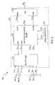
- FIG. 1 illustrates a conventional signal monitoring system 100.
- the signal monitoring system 100 includes a differential resistor-capacitor (RC) low-pass filter (LPF) 102 and a differential analog-to-digital converter (ADC) 104.
- the differential ADC 104 includes input terminals INP and INN coupled to the differential RC LPF 102.
- the RC LPF 102 receives an input signal V IN , blocks or attenuates high-frequency noises mixed in the input signal V IN , and passes a low-frequency portion V' IN of the input signal V IN to the ADC 104.
- the bandwidth of the RC LPF 102 needs to increase.
- the larger the bandwidth of the RC LPF 102 the more the noise mixed in the input signal V IN can be passed to the ADC 104.
- increasing the bandwidth of the RC LPF 102 filter can decrease the monitoring accuracy of the signal monitoring system 100.
- the bandwidth of the RC LPF 102 needs to decrease.
- the narrower the bandwidth of the RC LPF 102 the slower the response speed of the RC LPF 102.
- a signal filter includes a node, a first terminal, a second terminal, and energy storage circuitry coupled to the node and the first and second terminals.
- the node receives an input signal and a reference signal selectively.
- the first terminal provides an output signal determined by the input signal and the reference signal.
- the second terminal receives a feedback signal indicative of the output signal.
- the energy storage circuitry generates the output signal at the first terminal according to the input signal and the reference signal.
- the energy storage circuitry also receives the input signal via the node and the feedback signal via the second terminal in alternating fashion.
- a dominant pole of the signal filter is controlled by the frequency at which the input signal and the feedback signal alternate.
- a method for filtering a first input signal using a signal filter comprises: receiving, at energy storage circuitry, said first input signal and a first reference signal selectively; generating a first output signal according to said first input signal and said first reference signal; receiving, at said energy storage circuitry, a feedback signal indicative of said first output signal, wherein said first input signal and said feedback signal are received at said energy storage circuitry in alternating fashion; and controlling a dominant pole of said signal filter by controlling the frequency at which said first input signal and said feedback signal are received at said energy storage circuitry.
- a signal monitoring system comprises a signal filter operable for generating a first output signal according to a first input signal and a first reference signal and receiving a feedback signal indicative of said first output signal, said signal filter comprising a plurality of switches to deliver said first input signal and said reference signal to energy storage circuitry in said signal filter selectively, and deliver said first input signal and said feedback signal to said energy storage circuitry selectively; said signal monitoring system further comprising a signal generator coupled to said signal filter and operable for generating a control signal to control said plurality of switches, and controlling a frequency of said control signal to control a dominant pole of said signal filter.
- said signal monitoring system may further comprise an analog-to-digital converter coupled to said signal filter and operable for generating a digital signal indicative of a difference between said first output signal and a second output signal of said signal filter.
- said energy storage circuitry may comprise switched-capacitor circuitry.
- said control signal may control said switches so that, in a first time interval, a capacitor receives said first input signal via a first end of said capacitor and may receive a second reference signal via a second end of said capacitor, and wherein in a second time interval, said capacitor may receive said first reference signal via said first end and may provide said first output signal via said second end.
- a difference between said first output signal and a second output signal of said signal filter may be indicative of a difference between said first input signal and a second input signal of said signal filter minus a predetermined level that is within a range of said difference between said first and second input signals.
- said signal monitoring system may further comprise a multiplexer to select said first input signal from a plurality of signals.
- said signal generator may control said control signal to have a first frequency when said first input signal is switched from a first signal of said plurality of signals to a second signal of said plurality of signals, and may control said control signal to have a second frequency that is less than said first frequency when a time interval expires.
- FIG. 1 illustrates a conventional signal monitoring system.
- FIG. 2 illustrates a block diagram of an example of a battery monitoring system, in accordance with one embodiment of the present invention.
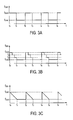
- FIGs. 3A to 3C illustrate frequency diagrams of examples of a clock signal, in accordance with embodiments of the present invention.
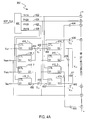
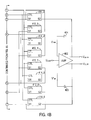
- FIGs. 4A and 4B illustrate a circuit diagram of an example of a switched-capacitor filter, in accordance with one embodiment of the present invention.
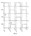
- FIG. 5 illustrates waveform diagrams of examples of clock signals. in accordance with one embodiment of the present invention.
- FIGs. 6A and 6B illustrate diagrams of examples of equivalent circuits of the switched-capacitor filter in FIGs. 4A and 4B , in accordance with one embodiment of the present invention.
- FIG. 7 illustrates a flowchart of examples of operations performed by a signal monitoring system, in accordance with one embodiment of the present invention.
- the present invention provides a signal monitoring system that includes a differential filter and a differential conversion circuit, e.g., an analog-to-digital converter (ADC).
- the signal monitoring system controls a dominant pole of the filter so as to control a bandwidth of the filter.
- the filter can control the level of a differential input signal of the ADC, such that the differential input range of the ADC is fully utilized.
- the differential input range of the ADC can also be reduced to enhance the measurement precision of the ADC.
- FIG. 2 illustrates a block diagram of an example of a battery monitoring system 200, in accordance with one embodiment of the present invention.
- the battery monitoring system 200 includes a set of cells 240_1, 240_2,..., 240_N, e.g., Lithium-lon battery cells or lead-acid battery cells.
- the battery monitoring system 200 further includes a signal monitoring system 250 operable for monitoring cell voltages of the cells 240_1-240_N.
- the signal monitoring system 250 includes a multiplexer 210, a signal filter 202, e.g., a switched-capacitor (SC) filter, an ADC 220, e.g., a differential ADC, and a signal generator 230.
- the signal filter 202 is a differential switched-capacitor low-pass filter.
- the multiplexer 210 receives a set of signals V IN(1) , V IN(2) , ..., V IN(N) , and a signal reference V REF0 , and provides input signals V INN and V INP to the signal filter 202.
- the signal reference V REF0 is used as the common ground for the signals V IN(1) , V IN(2) , ..., V IN(N) .
- the signal reference V REF0 can be grounded or provided by a voltage reference source (not shown in FIG. 2 ).
- the input signals V IN(1) , V IN(2) , ...,V IN(N) are terminal voltages at the positive terminals of the cells 240_1-240_N, respectively, and the signal reference V REF0 is grounded.
- the input signal V INN can be grounded.
- the signal filter 202 receives a single-ended signal, e.g., the input signal V INP , and generates a differential output signal to the ADC 220.
- the input signal V INP can be selected from cell voltages V 1 , V 2 , ..., V N of the cells 240_1, 240_2,..., 240_N.
- the multiplexer 210 receives the terminal voltages V IN(1) , V IN(2) , ..., V IN(N) and the signal reference V REF0 , and generates the cell voltages V 1 , V 2 , ..., V N that are respectively equal to the differences V IN(1) ⁇ V REF0 , V IN(2) ⁇ V IN(1) ,...,V IN(N) -V IN(N-1) .
- the multiplexer 210 further selects the input signal V INP from the cell voltages V 1 , V 2 , ..., V N and delivers the input signal V INP to the signal filter 202.
- the input signals V INN and V INP are selected from the signals V IN(1) , V IN(2) , ..., V IN(N) and V REF0 .
- the multiplexer 210 includes a set of switching channels to deliver two signals selected from the signals V IN(1) , V IN(2) , ..., V IN(N) and V REF0 to the signal filter 202.
- the set of switching channels can have various structures.
- the multiplexer 210 turns on two switching channels to deliver the signals V IN(1) and V REF0 to the signal filter 202, such that the signal filter 202 receives a differential input signal V IN(1) ⁇ V REF0 , e.g., the cell voltage V 1 .
- the multiplexer 210 can turn on the switching channels sequentially, such that the signal filter 202 can receive the cells voltages V 1 , V 2 , ..., V N sequentially.
- the signal filter 202 includes an input terminal INP1 to receive a first input signal V INP , an input terminal INN1 to receive a second input signal V INN , an output terminal OUTN1 to provide an output signal V OUTN , and an output terminal OUTP1 to provide an output signal V OUTP .
- the signal filter 202 receives a differential input signal that is equal to the difference between the input signals V INN and V INP , and generates a differential output signal that is equal to the difference between the output signals V OUTN and V OUTP .
- the differential output signal V OUTP -V OUTN indicates the differential input signal V INP ⁇ V INN , e.g., the difference V OUTP -V OUTN is proportional to the difference V INP ⁇ V INN .
- the ADC 220 receives the differential output signal V OUTP ⁇ V OUTN and generates a digital signal 226 indicative of the differential output signal V OUTP ⁇ V OUTN , which also indicates the differential input signal V INP ⁇ V INN.
- the signal generator 230 can be a clock signal generator that includes one or more oscillators to generate control signals such as clock signals CLK1 and CLK2 to control the signal filter 202.
- the clock signals CLK1 and CLK2 control a dominant pole (or a first pole) f p0 of the signal filter 202 according to a status of the differential input signal V INP ⁇ V INN .
- the signal generator 230 is arranged outside of the signal filter 202. However, the signal generator 230 can instead be arranged inside the signal filter 202.
- a differential output range of the signal filter 202 can be controlled such that the signal monitoring system 250 can fully utilize a differential input range of the ADC 220 and decrease the differential input range of the ADC 220, so as to enhance the measurement precision of the ADC 220.
- the response speed of the signal monitoring system 250 e.g., the speed at which the output signals V OUTN and V OUTP vary in response to variations in the input signals V INN and V INP .
- the monitoring accuracy of the signal monitoring system 250 e.g., the accuracy of the digital signal 226 indicating the difference between the input signals V INN and V INP , is also improved.
- the signal filter 202 receives the first and second input signals V INP and V INN , and generates a first output signal V [NN and a second output signal V' INP (not shown in FIG. 2 ) according to the input signals V INN and V INP and according to a reference signal V REFH and a reference signal V REFL .
- the reference signals V REFH and V REFL can be provided by reference signal sources (not shown in FIG. 2 ) implemented inside or outside of the signal filter 202.
- the signal filter 202 controls a voltage level of the output signal V INN and a voltage level of the output signal V' INP , such that the difference between the output signals V' INN and V' INP is equal to the difference between the input signals V INN and V INP minus the difference between the reference signals V REFH and V REFL .
- the signal filter 202 receives a differential input signal V INP -V INN , transforms the differential input signal V INP -V INN into a differential signal V' INP -V' INN , and generates a differential output signal V OUTP -V OUTN that is equal to the differential signal V' INP -V' INN multiplied by a gain g 202 of the signal filter 202.
- the reference signals V REFH and V REFL are set such that the difference V REFH ⁇ V REFL is within the range of the differential input signal V INP ⁇ V INN .
- the maximum absolute value of the difference V' INP ⁇ V' INN e.g., the maximum of the level
- the differential input range of the ADC 220 can be reduced.
- the differential input signal V INP ⁇ V INN ranges from 0V to a maximum level V MAX .
- V OUTP - V OUTN V INP - V INN - V MAX / 2 * g 202 . Since the differential input signal V INP ⁇ V INN ranges from 0V to the maximum level V MAX , the differential output signal V OUTP ⁇ V OUTN can range from the level -(V MAX /2) * g 202 to the level (V MAX /2)*g 202 .
- the ADC 220 generates a digital signal DIG IN representative of the differential output signal V OUTP ⁇ V OUTN , and generates the digital signal 226 that is equal to the digital signal DIG IN plus a reference digital signal DIG REF .
- the reference digital signal DIG REF represents the difference V REFH ⁇ V REFL .
- the digital signal 226 represents the differential input signal V INP ⁇ V INN .
- the signal filter 202 includes a switched-capacitor circuit.
- a control signal SCF_CLK selected from the clock signals CLK1 and CLK2 controls, e.g., alternately turns on and off, switches in the switched-capacitor circuit, so as to provide an equivalent resistance R sc .
- the signal filter 202 is a low-pass filter.
- the equivalent resistance R EQV of the signal filter 202 is provided by the switched-capacitor circuit, and therefore is equal to the equivalent resistance R SC of the switched-capacitor circuit.
- f p ⁇ 0 f CLK * C SC / 2 ⁇ ⁇ * C EQV .
- the signal generator 230 can increase the frequency F CLK of the control signal SCF_CLK to increase the dominant pole f p0 of the signal filter 202, and therefore to increase the bandwidth of the signal filter 202.
- the signal generator 230 can also decrease the frequency f CLK to decrease the dominant pole f p0 , and therefore to decrease the bandwidth of the signal filter 202.
- FIG. 3A illustrates a frequency diagram of an example of the control signal SCF_CLK that controls the switches in the signal filter 202, in accordance with one embodiment of the present invention.
- FIG. 3A is described in combination with FIG. 2 .
- the frequency f CLK of the control signal SCF_CLK can have a frequency f CLK1 and a frequency f CLK2 that is less than the frequency f CLK1 .
- the signal generator 230 selects the control signal SCF_CLK from the clock signals CLK1 and CLK2 to control the dominant pole f p0 of the signal filter 202 according to the status of the differential input signal V INP ⁇ V INN .
- the clock signal CLK1 has the frequency f CLK1
- the clock signal CLK2 has the frequency f CLK2 .
- the multiplexer 210 can select and deliver a cell voltage from the cell voltages V 1 , V 2 , ..., V N to the signal filter 202 sequentially, such that the signal monitoring system 250 can monitor each of the cell voltages V 1 , V 2 , ..., V N .
- the signal generator 230 selects the clock signal CLK1 that has the frequency f CLK1 to control the signal filter 202.
- the signal generator 230 can include a timer to count time.
- the signal generator 230 selects the clock signal CLK2 that has the frequency f CLK2 to control the signal filter 202.
- the differential input signal V INP -V INN can be switched from the second signal (e.g., the cell voltage V 2 ) to a third signal (e.g., the cell voltage V 3 ).
- the signal generator 230 selects the clock signal CLK1 to control the signal filter 202 again.
- the signal filter 202 can increase its bandwidth to increase the response speed.
- the signal filter 202 can decrease its bandwidth to enhance the accuracy of the ADC 220.
- the signal generator 230 selects the control signal SCF_CLK from the clock signals CLK1 and CLK2 to control the signal filter 202.
- the invention is not so limited.
- FIG. 3B and FIG. 3C illustrate frequency diagrams of other examples of the control signal SCF_CLK, in accordance with embodiments of the present invention.
- FIG. 3B and FIG. 3C are described in combination with FIG. 2 .
- the signal generator 230 selects the control signal SCF_CLK from three or more clock signals that have different frequencies, e.g., f CLK1 , f 1 , f 2 , and f CLK2 , to control the signal filter 202.
- the signal generator 230 controls the control signal SCF_CLK to have a higher frequency f CLK1 when the differential input signal V INP -V INN is switched from one signal to another signal, e.g., at time to, t 2 , t 4 , etc., and then decreases the frequency of the control signal SCF_CLK to a lower frequency f CLK2 continuously as shown in FIG. 3C .
- FIGs. 4A and 4B illustrate a circuit diagram of an example of the signal filter 202 in FIG. 2 , in accordance with one embodiment of the present invention.
- the signal filter 202 includes filter circuitry and a differential amplification circuitry 402 coupled to the filter circuitry.
- the filter circuitry includes multiple switches 416_1-416_2, 418_1-418_2, 412_1-412_6 and 414_1-414_6, multiple capacitors 432, 442, 434, 444, 436, 446, 438, 448, 404 and 406, and a set of signal lines 422, 424, 428 and 426.
- each switch of the switches 416_1-416_2, 418_1-418_2, 412_1-412_6 and 414_1-414_6 includes a control terminal labeled "CTL" (hereinafter, CTL terminal), a terminal labeled "S1” (hereinafter, S1 terminal), and a terminal labeled "S2" (hereinafter, S2 terminal).
- CTL terminal control terminal labeled "CTL”
- S1 terminal hereinafter, S1 terminal
- S2 terminal labeled "S2”
- a control signal at the CTL terminal can control the status of the switch. For example, if the control signal is logic high, the switch is turned on and a signal can be transferred between the S1 terminal and the S2 terminal. If the control signal is logic low, the switch is turned off.
- a first end 452 of the capacitor 432 is coupled to receive the input signal V INP via the switch 416_1 and is coupled to receive the reference signal V REFH via the switch 418_1.
- a second end 454 of the capacitor 432 is coupled to receive a reference signal, e.g., the reference signal V REFH or another reference signal V' REF not shown in FIG. 4A , via the switch 412_1, and is coupled to provide the output signal V' INN via the capacitor 436 and the switch 414_4.
- a first end 456 of the capacitor 442 is coupled to receive the input signal V INN via the switch 416_2 and is coupled to receive the reference signal V REFL via the switch 418_2.
- a second end 458 of the capacitor 442 is coupled to receive the same reference signal that is received by the switch 412_1, e.g., the reference signal V REFH or the reference signal V' REF not shown in FIG. 4A , via the switch 412_2, and is coupled to provide the output signal V' INP via the capacitor 446 and the switch 414_5.
- two ends of each of the capacitors 434, 436, 446 and 444 are coupled to receive the same reference signal that is received by the switches 412_1 and 412_2, e.g., the reference signal V REFH or the reference signal V' REF not shown in FIG. 4A , via corresponding switches 412_1-412_6.
- the capacitors 434 and 444 are also coupled to receive feedback signals V OUTN and V OUTP via the switches 414_3 and 414_6 respectively.
- the switches 414_1 and 414_2 are coupled to control the capacitors 438 and 448.
- the filter circuitry receives the input signals V INN and V INP and the reference signals V REFH and V REFL through input capacitors 432 and 442, and receives feedback signals V OUTN and V OUTP through feedback capacitors 434 and 444.
- the filter circuitry further generates the output signals V' INN and V' INP in accordance with equation (1).
- the differential amplification circuitry 402 receives the outputs signals V' INN and V' INP and generates the output signals V OUTN and V OUTP in accordance with equations (3a) and (3b).
- the signal filter 202 receives the control signal SCF_CLK to control the switches 416_1-416_2. 418_1-418_2, 412_1-412_6 and 414_1-414_6, such that the signal filter 202 receives the input signal V INP and the reference signal V REFH via the node 452 in alternating fashion and generates the output signal V' INN determined by the input signal V INP and the reference signal V REFH .
- the signal filter 202 can also receive the input signal V INN and the reference signal V REFL via the node 456 in alternating fashion and generates the output signal V' INP determined by the input signal V INN and the reference signal V REFL .
- the difference between the output signals V' INP and V' INN can be given by equation (1).
- the signal filter 202 receives the differential input signal V INP ⁇ V INN and the differential output signal V OUTP ⁇ V OUTN in alternating fashion, such that an equivalent resistance of the signal filter 202 is controlled by the frequency at which the differential input signal V INP ⁇ V INN and the differential output signal V OUTP ⁇ V OUTN alternate, e.g., the frequency f CLK of the control signal SCF_CLK, in accordance with equation (5).
- the dominant pole f p0 of the signal filter 202 is controlled by controlling the frequency F CLK of the control signal SCF_CLK.
- the switches 416_1 and 416_2 are coupled to the signal line 426 and controlled by a clock signal PH1B at the signal line 426.
- the switches 418_1 and 418_2 are coupled to the signal line 428 and controlled by a clock signal PH2B at the signal line 428.
- the switches 412_1-412_2 (in FIG. 4A ) and the switches 412__3-412_6 (in FIG. 4B ) are coupled to the signal line 422 and controlled by a clock signal PH1A at the signal line 422.
- the switches 414_1-414_2 (in FIG. 4A ) and the switches 414_3-414_6 (in FIG. 4B ) are coupled to the signal line 424 and controlled by a clock signal PH2A at the signal line 424.
- a non-overlapping clock generator 450 can receive the control signal SGF_CLK, e.g. a clock signal, and generate clock signals PH1A, PH2A, PH1B and PH2B with the frequency f CLK of the control signal SCF_CLK or with a frequency that is directly proportional to the frequency f CLK .
- the non-overlapping clock generator 450 also controls phase differences between the clock signals PH1A, PH2A, PH1B and PH2B. Examples of waveforms of the clock signals PH1A, PH2A, PH1B and PH2B are illustrated in FIG. 5 , in accordance with one embodiment of the present invention.
- the clock signals PH1A and PH2A are a pair of non-overlapping signals
- the clock signals PH1B and PH2B are a pair of non-overlapping signals. More specifically, if the clock signal PH1A is logic high, the clock signal PH2A is logic low; if the clock signal PH2A is logic high, the clock signal PH1A is logic low. Similarly, if the clock signal PH1B is logic high, the clock signal PH2B is logic low; if the clock signal PH2B is logic high, the clock signal PH1B is logic low.
- the clock signal PH1B is a delayed version of the clock signal PH1A
- the clock signal PH2B is a delayed version of the clock signal PH2A.
- a rising edge of the clock signal PH1A occurs at time t P0
- a corresponding rising edge of the clock signal PH1B occurs at time tp 1 that is ⁇ t delayed from the time t P0
- the clock signals PH1A and PH1B have the same duty cycle.
- a rising edge of the clock signal PH2A occurs at time t P4
- a corresponding rising edge of the clock signal PH2B occurs at time t P5 that is At delayed from the time t P4 .
- the clock signals PH2A and PH2B have the same duty cycle. Compared with cycle times of the clock signals PH1A, PH2A, PH1B and PH2B, the delayed time At is relatively short.
- the clock signals PH1A and PH1B are logic high, and the clock signals PH2A and PH2B are logic low. Accordingly, the switches 416_1-416_2 and the switches 412_1-412_6 are on, and the switches 418_1-418_2 and the switches 414_1-414_6 are off.
- An example of an equivalent circuit 600 of the signal filter 202 during the time interval t P1 to t P2 is shown in FIG. 6A .
- the clock signals PH1A and PH1B are logic low, and the clock signals PH2A and PH2B are logic high.
- switches 416_1-416_2 and the switches 412_1-412_6 are off, and the switches 418_1-418_2 and the switches 414_1-414_6 are on.
- An example of an equivalent circuit 600' of the signal filter 202 during the time interval t P5 to t P6 is shown in FIG. 6B .
- the capacitor 432 receives the input signal V INP via the first end 452 of the capacitor 432 and receives the reference signal V REFH via the second end 454 of the capacitor 432.
- the capacitor 442 receives the input signal V INN via the first end 456 of the capacitor 442 and receives the reference signal U REFH via the second end 458 of capacitor 442.
- two ends of each of the capacitors 434, 436, 446 and 444 receive the reference signal V REFH . Voltages across the capacitors 434, 436, 446 and 444 are zero volts.
- the capacitor 432 receives the reference signal V REFH via the first end 452 of the capacitor 432 and provides the output signal V' INN which is transferred to the differential amplification circuitry 402 via the second end 454 of the capacitor 432 and via the capacitor 436.
- the capacitor 442 receives the reference signal V REFL via the first end 456 of the capacitor 442 and provides the output signal V' INP which is transferred to the differential amplification circuitry 402 via the second end 458 of the capacitor 442 and via the capacitor 446.
- the voltage at the second end 454 of the capacitor 432 can be equal to the reference signal V REFH plus the level V REFH ⁇ V INP
- the output signal V' INN can be equal to the level V REFH +V REFH ⁇ V INP plus zero volts.
- the voltage at the second end 458 of the capacitor 442 can be equal to the reference signal V REFL plus the level V REFH ⁇ V INN
- the output signal V' INP can be equal to the level V REFL +V REFH ⁇ V INP plus zero volts.
- the node 452 of the energy storage circuitry 602 receives the input signal V INP and the reference signal V REFH selectively.
- the node 456 of the energy storage circuitry 602 can receive input signal V INN and the reference signal V REFL selectively.
- the S2 terminal of the switch 414_4 provides the output signal V' INN determined by the input signal V INP and the reference signal V REFH .
- the S2 terminal of the switch 414_5 provides the output signal V' INP determined by the input signal V INN and the reference signal V REFL .
- the S2 terminal of the switch 414_3 receives the feedback signal V OUTN indicative of the output signal V' INN .
- the S2 terminal of the switch 414_6 receives the feedback signal V OUTP indicative of the output signal V' INP .
- the energy storage circuitry 602 generates the output signal V' INN at the S2 terminal of the switch 414_4 and the output signal V' INP at the S2 terminal of the switch 414_5. The difference between the output signals V' INN and V' INP is obtained in accordance with equation (1).
- the second end 454 of the capacitor 432, the second end 458 of the capacitor 442, and the four ends of the capacitors 436 and 446 receive the reference signal V REFH in the first time interval, e.g., t P1 to t P2
- the invention is not so limited.
- the first end 452 of the capacitor 432 receives the input signal V INP
- the first end 456 of the capacitor 442 receives the input signal V INN .
- the second end 454 of the capacitor 432, the second end 458 of the capacitor 442, and the four ends of the capacitors 436 and 446 receive another reference signal V' REF instead of the reference signal V REFH .
- the first end 452 of the capacitor 432 receives the reference signal V REFH
- the first end 456 of the capacitor 442 receives the reference signal V REFL .
- the second end 454 of the capacitor 432 provides the output signal V' INN via the capacitor 436
- the second end 458 of the capacitor 442 provides the output signal V' INP via the capacitor 446.
- V ⁇ INN V REFH + V ⁇ REF - V INP ;
- V ⁇ INP V REFL + V ⁇ REF - V INN .
- the difference between the output signals V' INN and V' INP can also be obtained in accordance with equation (1).
- the energy storage circuitry 602 can receive the input signal V INP via the node 452 and the feedback signal V OUTP via the S2 terminal of the switch 414_3 in alternating fashion, and receive the input signal V INN via the node 456 and the feedback signal V OUTN via the S2 terminal of the switch 414_6 in alternating fashion.
- the dominant pole f p0 of the signal filter 202 is controlled by the frequency at which the input signal V INP and the feedback signal V OUTP alternate or the frequency at which the input signal V INN and the feedback signal V OUTN alternate.
- charge stored in the energy storage circuitry 602 that includes the capacitors 432, 442, 434, 444, 436 and 446 is controlled by the differential input signal V INP -V INN .
- charge Q SC stored in the energy storage circuitry 602 is given by C sc *(V INP ⁇ V INN ).
- C SC represents a capacitive parameter in the energy storage circuitry 602.
- V OUTP -V OUTN As shown in FIG. 6B , during the time interval t P5 to t P6 , charge stored in the energy storage circuitry 602 is controlled by the differential output signal V OUTP -V OUTN .
- charge Q' SC stored in the energy storage circuitry 602 is given by C SC *(V OUTP ⁇ V OUTN ).
- the control signal SCF_CLK can control the switches 416_1-416_2, 418_1-418_2, 412_1-412_6 and 414_1-414_6, such that charge stored in the energy storage circuitry 602 is controlled by the differential input signal V INP ⁇ V INN and the differential output signal V OUTP ⁇ V OUTN alternately with the frequency F CLK .
- capacitances of the capacitors 438, 448, 404 and 406 can be equal to C 0
- capacitances of the capacitors 432, 442, 434 and 444 can be equal to 0.5*C 1
- capacitances of the capacitors 436 and 446 can be equal to C 1
- f' CLK represents the switching frequency of the switches 416_1-416_2, 418_1-418_2, 412_1-412_6 and 414_1-414_6.
- the dominant pole f p0 of the signal filter 202 can be controlled by controlling the frequency f CLK of the control signal SCF_CLK.
- the signal filter 202 includes the switches 418_2 and 416_2.
- the switches 418_2 and 416_2 can be omitted.
- the reference signal V REFL and the input signal V INP can be grounded.
- the signal filter 202 can receive a single-ended input signal V INP and generate a differential output signal V OUTP ⁇ V OUTN indicative of the input signal V INP .
- FIG. 7 illustrates a flowchart 700 of examples of operations performed by a signal monitoring system, in accordance with one embodiment of the present invention.
- FIG. 7 is described in combination with FIG. 2 , FIGs. 3A to 3C , FIGs. 4A and 4B , FIG. 5 , and FiGs. 6A and 6B .
- the input signal V INP and the reference signal V REFH are received at the energy storage circuitry 602, e.g., at the node 452, selectively.
- the input signal V INN and the reference signal V REFL are also received at the energy storage circuitry 602, e.g., at the node 456, selectively.
- the output signal V' INN is generated, e.g., at the S2 terminal of the switch 414_4, according to the input signal V INP and the reference signal V REFH , and the output signal V' INP is generated, e.g., at the S2 terminal of the switch 414_5, according to the input signal V INN and the reference signal V REFL .
- the feedback signal V OUTN indicative of the output signal V' INN is received at the energy storage circuitry 602, e.g., at the S2 terminal of the switch 414_3, and the feedback signal V OUTP indicative of the output signal V' INP is received at the energy storage circuitry 602, e.g., at the S2 terminal of the switch 414_6.
- the input signal V INP and the feedback signal V OUTN are received at the energy storage circuitry 602 in alternating fashion, and the input signal V INN and the feedback signal V OUTP are received at the energy storage circuitry 602.
- the energy storage circuitry 602 receives the differential input signal V INP ⁇ V INN and the differential feedback signal V OUTP -V OUTN in alternating fashion.
- the dominant pole f p0 of the signal filter 202 is controlled by controlling the frequency f CLK at which the differential input signal V INP -V INN and the differential feedback signal V OUTP ⁇ V OUTN are received at the energy storage circuitry 602.
- the present invention provides a signal monitoring system for monitoring an input signal.
- the signal monitoring system includes, in one embodiment, a switched-capacitor filter to filter the input signal and provides a differential output signal to an ADC.
- a clock signal controls switches in the signal filter, such that the differential output signal is controlled to be within a desired ranged for the ADC, and a dominant pole of the signal filter is controlled properly.
- the signal monitoring system can be used in various applications such as multiple-signal monitoring systems, battery monitoring systems, etc.
Landscapes
- Physics & Mathematics (AREA)
- General Physics & Mathematics (AREA)
- Manipulation Of Pulses (AREA)
- Measurement Of Current Or Voltage (AREA)
- Charge And Discharge Circuits For Batteries Or The Like (AREA)
- Filters That Use Time-Delay Elements (AREA)
- Circuits Of Receivers In General (AREA)
- Amplifiers (AREA)
- Networks Using Active Elements (AREA)
Priority Applications (1)
| Application Number | Priority Date | Filing Date | Title |
|---|---|---|---|
| EP15191103.9A EP2998755A1 (de) | 2010-06-22 | 2011-05-24 | Signalüberwachungssysteme |
Applications Claiming Priority (2)
| Application Number | Priority Date | Filing Date | Title |
|---|---|---|---|
| US35718110P | 2010-06-22 | 2010-06-22 | |
| US12/962,210 US8344794B2 (en) | 2010-06-22 | 2010-12-07 | Signal monitoring systems |
Related Child Applications (1)
| Application Number | Title | Priority Date | Filing Date |
|---|---|---|---|
| EP15191103.9A Division EP2998755A1 (de) | 2010-06-22 | 2011-05-24 | Signalüberwachungssysteme |
Publications (2)
| Publication Number | Publication Date |
|---|---|
| EP2403142A2 true EP2403142A2 (de) | 2012-01-04 |
| EP2403142A3 EP2403142A3 (de) | 2015-04-22 |
Family
ID=44650619
Family Applications (2)
| Application Number | Title | Priority Date | Filing Date |
|---|---|---|---|
| EP20110167313 Withdrawn EP2403142A3 (de) | 2010-06-22 | 2011-05-24 | Signalüberwachungssysteme |
| EP15191103.9A Withdrawn EP2998755A1 (de) | 2010-06-22 | 2011-05-24 | Signalüberwachungssysteme |
Family Applications After (1)
| Application Number | Title | Priority Date | Filing Date |
|---|---|---|---|
| EP15191103.9A Withdrawn EP2998755A1 (de) | 2010-06-22 | 2011-05-24 | Signalüberwachungssysteme |
Country Status (5)
| Country | Link |
|---|---|
| US (1) | US8344794B2 (de) |
| EP (2) | EP2403142A3 (de) |
| JP (1) | JP2012010329A (de) |
| CN (1) | CN102299699B (de) |
| TW (1) | TWI427924B (de) |
Families Citing this family (7)
| Publication number | Priority date | Publication date | Assignee | Title |
|---|---|---|---|---|
| US8643333B2 (en) * | 2011-08-31 | 2014-02-04 | Delphi Technologies, Inc. | Battery stack cell monitor |
| CN104237600A (zh) * | 2013-06-13 | 2014-12-24 | 同济大学 | 一种针对轨道交通车辆的能耗检测系统 |
| US10901045B2 (en) | 2018-03-16 | 2021-01-26 | Infineon Technologies Ag | Battery diagnostics system and method using second path redundant measurement approach |
| CN111308432B (zh) * | 2019-12-03 | 2022-03-22 | 中国人民解放军63921部队 | 一种利用测速数据评估航天器测距数据精度的方法 |
| CN111953306B (zh) * | 2020-08-26 | 2021-03-02 | 郑州工程技术学院 | 一种大数据多中心联合控制系统 |
| JP7678742B2 (ja) * | 2021-11-26 | 2025-05-16 | 株式会社デンソー | 電池監視システム |
| WO2025057936A1 (ja) * | 2023-09-12 | 2025-03-20 | ヌヴォトンテクノロジージャパン株式会社 | 電圧測定回路 |
Family Cites Families (11)
| Publication number | Priority date | Publication date | Assignee | Title |
|---|---|---|---|---|
| JPH07109977B2 (ja) * | 1986-12-18 | 1995-11-22 | 株式会社日立製作所 | スイツチトキヤパシタフイルタ |
| JP3799618B2 (ja) * | 1994-10-21 | 2006-07-19 | 株式会社デンソー | 信号処理回路 |
| US5574457A (en) * | 1995-06-12 | 1996-11-12 | Motorola, Inc. | Switched capacitor gain stage |
| US5736895A (en) * | 1996-01-16 | 1998-04-07 | Industrial Technology Research Institute | Biquadratic switched-capacitor filter using single operational amplifier |
| US6147551A (en) * | 1998-01-05 | 2000-11-14 | Motorola, Inc. | Switched capacitor circuit and method for reducing sampling noise |
| JP2004289802A (ja) * | 2003-03-06 | 2004-10-14 | Denso Corp | ローパスフィルタ及びそれを使用した半導体圧力センサ装置 |
| US7260491B2 (en) * | 2005-10-27 | 2007-08-21 | International Business Machines Corporation | Duty cycle measurement apparatus and method |
| US7812568B2 (en) * | 2006-12-07 | 2010-10-12 | Sanyo Electric Co., Ltd. | Voltage detecting circuit |
| JP5056490B2 (ja) * | 2008-03-10 | 2012-10-24 | 富士通株式会社 | 歪み補償係数更新装置および歪み補償増幅器 |
| JP4505027B2 (ja) * | 2008-05-08 | 2010-07-14 | 株式会社半導体理工学研究センター | サンプルホールド回路及びa/d変換装置 |
| US7990209B2 (en) * | 2009-06-19 | 2011-08-02 | Allegro Microsystems, Inc. | Switched capacitor notch filter |
-
2010
- 2010-12-07 US US12/962,210 patent/US8344794B2/en active Active
-
2011
- 2011-04-26 CN CN201110105423.6A patent/CN102299699B/zh active Active
- 2011-05-24 EP EP20110167313 patent/EP2403142A3/de not_active Withdrawn
- 2011-05-24 EP EP15191103.9A patent/EP2998755A1/de not_active Withdrawn
- 2011-05-30 JP JP2011120281A patent/JP2012010329A/ja not_active Withdrawn
- 2011-06-21 TW TW100121548A patent/TWI427924B/zh not_active IP Right Cessation
Also Published As
| Publication number | Publication date |
|---|---|
| CN102299699A (zh) | 2011-12-28 |
| JP2012010329A (ja) | 2012-01-12 |
| EP2403142A3 (de) | 2015-04-22 |
| TWI427924B (zh) | 2014-02-21 |
| EP2998755A1 (de) | 2016-03-23 |
| US8344794B2 (en) | 2013-01-01 |
| CN102299699B (zh) | 2014-07-30 |
| US20110309880A1 (en) | 2011-12-22 |
| TW201214956A (en) | 2012-04-01 |
Similar Documents
| Publication | Publication Date | Title |
|---|---|---|
| EP2403142A2 (de) | Signalüberwachungssysteme | |
| US6473018B2 (en) | Delta sigma analog-to-digital converter | |
| JP5009919B2 (ja) | A/d変換器 | |
| US9104266B2 (en) | Signal processing circuit and signal processing system of touch screen | |
| US20090212826A1 (en) | Hysteresis comparator | |
| US20120001683A1 (en) | Voltage level shift circuits and methods | |
| US10630245B2 (en) | Capacitively coupled chopper amplifier | |
| US10115475B2 (en) | Compensation circuit for compensating for an input charge in a sample and hold circuit | |
| JP2017156194A (ja) | 電圧検出装置および組電池監視システム | |
| US9397645B2 (en) | Circuit for common mode removal for DC-coupled front-end circuits | |
| EP3379726A1 (de) | Analog-digital-umsetzer, sensoranordnung und verfahren zur analog-digital-umsetzung | |
| JP4785801B2 (ja) | D級増幅器 | |
| CN102005917A (zh) | 一种恒压输出电荷泵电路 | |
| US7157945B2 (en) | Window comparator and method of providing a window comparator function | |
| JP2019149762A (ja) | 逐次比較型ad変換器およびセンサ装置 | |
| CN111817553B (zh) | 片内式电荷泵电路 | |
| EP2262106A1 (de) | Schaltung für einen Verstärker | |
| JP5499431B2 (ja) | 三角波発生回路 | |
| JP5835073B2 (ja) | Cv変換回路 | |
| EP4651379A2 (de) | Kapazitives ladeverfahren und schaltung für einen differenzialkomparator für einen analog-digital-wandler | |
| CN120238097A (zh) | 载波发生器、开关电源和包络跟踪调制器 | |
| US20240364288A1 (en) | Systems, methods, and devices for direct sampling in data converters | |
| JP2008304255A (ja) | 半導体装置 | |
| JP2012112873A (ja) | 周波数計測回路 | |
| JP2007274743A (ja) | 発振回路 |
Legal Events
| Date | Code | Title | Description |
|---|---|---|---|
| AK | Designated contracting states |
Kind code of ref document: A2 Designated state(s): AL AT BE BG CH CY CZ DE DK EE ES FI FR GB GR HR HU IE IS IT LI LT LU LV MC MK MT NL NO PL PT RO RS SE SI SK SM TR |
|
| AX | Request for extension of the european patent |
Extension state: BA ME |
|
| PUAI | Public reference made under article 153(3) epc to a published international application that has entered the european phase |
Free format text: ORIGINAL CODE: 0009012 |
|
| RIC1 | Information provided on ipc code assigned before grant |
Ipc: H03H 19/00 20060101AFI20141128BHEP Ipc: G01R 31/36 20060101ALN20141128BHEP |
|
| PUAL | Search report despatched |
Free format text: ORIGINAL CODE: 0009013 |
|
| AK | Designated contracting states |
Kind code of ref document: A3 Designated state(s): AL AT BE BG CH CY CZ DE DK EE ES FI FR GB GR HR HU IE IS IT LI LT LU LV MC MK MT NL NO PL PT RO RS SE SI SK SM TR |
|
| AX | Request for extension of the european patent |
Extension state: BA ME |
|
| RIC1 | Information provided on ipc code assigned before grant |
Ipc: H03H 19/00 20060101AFI20150319BHEP Ipc: G01R 31/36 20060101ALN20150319BHEP |
|
| STAA | Information on the status of an ep patent application or granted ep patent |
Free format text: STATUS: THE APPLICATION IS DEEMED TO BE WITHDRAWN |
|
| 18D | Application deemed to be withdrawn |
Effective date: 20151023 |