EP2399114B1 - Sensor network incorporating stretchable silicon - Google Patents
Sensor network incorporating stretchable silicon Download PDFInfo
- Publication number
- EP2399114B1 EP2399114B1 EP10701948.1A EP10701948A EP2399114B1 EP 2399114 B1 EP2399114 B1 EP 2399114B1 EP 10701948 A EP10701948 A EP 10701948A EP 2399114 B1 EP2399114 B1 EP 2399114B1
- Authority
- EP
- European Patent Office
- Prior art keywords
- sensors
- stretchable
- sensor
- energy harvesting
- silicon substrate
- Prior art date
- Legal status (The legal status is an assumption and is not a legal conclusion. Google has not performed a legal analysis and makes no representation as to the accuracy of the status listed.)
- Active
Links
- 229910052710 silicon Inorganic materials 0.000 title claims description 67
- 239000010703 silicon Substances 0.000 title claims description 67
- XUIMIQQOPSSXEZ-UHFFFAOYSA-N Silicon Chemical compound [Si] XUIMIQQOPSSXEZ-UHFFFAOYSA-N 0.000 claims description 66
- 238000004891 communication Methods 0.000 claims description 40
- 238000003306 harvesting Methods 0.000 claims description 26
- 238000003860 storage Methods 0.000 claims description 23
- 239000000758 substrate Substances 0.000 claims description 23
- 238000012545 processing Methods 0.000 claims description 17
- 238000000034 method Methods 0.000 claims description 15
- 238000012544 monitoring process Methods 0.000 claims description 13
- XLOMVQKBTHCTTD-UHFFFAOYSA-N Zinc monoxide Chemical compound [Zn]=O XLOMVQKBTHCTTD-UHFFFAOYSA-N 0.000 claims description 9
- 239000004020 conductor Substances 0.000 claims description 6
- 238000000926 separation method Methods 0.000 claims description 4
- 230000006870 function Effects 0.000 description 4
- 239000002070 nanowire Substances 0.000 description 4
- 230000003750 conditioning effect Effects 0.000 description 3
- 238000010586 diagram Methods 0.000 description 3
- 238000005516 engineering process Methods 0.000 description 3
- 229920001746 electroactive polymer Polymers 0.000 description 2
- 238000004146 energy storage Methods 0.000 description 2
- 239000000835 fiber Substances 0.000 description 2
- 230000010354 integration Effects 0.000 description 2
- 210000003205 muscle Anatomy 0.000 description 2
- 239000011787 zinc oxide Substances 0.000 description 2
- 238000010276 construction Methods 0.000 description 1
- 238000011161 development Methods 0.000 description 1
- 230000000694 effects Effects 0.000 description 1
- 231100001261 hazardous Toxicity 0.000 description 1
- 238000009434 installation Methods 0.000 description 1
- 238000011031 large-scale manufacturing process Methods 0.000 description 1
- 238000004519 manufacturing process Methods 0.000 description 1
- 239000000463 material Substances 0.000 description 1
- 238000004377 microelectronic Methods 0.000 description 1
- 230000003287 optical effect Effects 0.000 description 1
- 239000005022 packaging material Substances 0.000 description 1
- 229920001296 polysiloxane Polymers 0.000 description 1
- 238000010248 power generation Methods 0.000 description 1
- 238000003786 synthesis reaction Methods 0.000 description 1
Images

Classifications
-
- G—PHYSICS
- G01—MEASURING; TESTING
- G01M—TESTING STATIC OR DYNAMIC BALANCE OF MACHINES OR STRUCTURES; TESTING OF STRUCTURES OR APPARATUS, NOT OTHERWISE PROVIDED FOR
- G01M5/00—Investigating the elasticity of structures, e.g. deflection of bridges or air-craft wings
-
- B—PERFORMING OPERATIONS; TRANSPORTING
- B82—NANOTECHNOLOGY
- B82B—NANOSTRUCTURES FORMED BY MANIPULATION OF INDIVIDUAL ATOMS, MOLECULES, OR LIMITED COLLECTIONS OF ATOMS OR MOLECULES AS DISCRETE UNITS; MANUFACTURE OR TREATMENT THEREOF
- B82B3/00—Manufacture or treatment of nanostructures by manipulation of individual atoms or molecules, or limited collections of atoms or molecules as discrete units
- B82B3/0009—Forming specific nanostructures
- B82B3/0014—Array or network of similar nanostructural elements
-
- B—PERFORMING OPERATIONS; TRANSPORTING
- B82—NANOTECHNOLOGY
- B82Y—SPECIFIC USES OR APPLICATIONS OF NANOSTRUCTURES; MEASUREMENT OR ANALYSIS OF NANOSTRUCTURES; MANUFACTURE OR TREATMENT OF NANOSTRUCTURES
- B82Y30/00—Nanotechnology for materials or surface science, e.g. nanocomposites
-
- B—PERFORMING OPERATIONS; TRANSPORTING
- B82—NANOTECHNOLOGY
- B82Y—SPECIFIC USES OR APPLICATIONS OF NANOSTRUCTURES; MEASUREMENT OR ANALYSIS OF NANOSTRUCTURES; MANUFACTURE OR TREATMENT OF NANOSTRUCTURES
- B82Y40/00—Manufacture or treatment of nanostructures
-
- H—ELECTRICITY
- H01—ELECTRIC ELEMENTS
- H01L—SEMICONDUCTOR DEVICES NOT COVERED BY CLASS H10
- H01L21/00—Processes or apparatus adapted for the manufacture or treatment of semiconductor or solid state devices or of parts thereof
- H01L21/02—Manufacture or treatment of semiconductor devices or of parts thereof
- H01L21/02104—Forming layers
- H01L21/02365—Forming inorganic semiconducting materials on a substrate
- H01L21/02518—Deposited layers
- H01L21/02587—Structure
- H01L21/0259—Microstructure
- H01L21/02603—Nanowires
-
- B—PERFORMING OPERATIONS; TRANSPORTING
- B82—NANOTECHNOLOGY
- B82Y—SPECIFIC USES OR APPLICATIONS OF NANOSTRUCTURES; MEASUREMENT OR ANALYSIS OF NANOSTRUCTURES; MANUFACTURE OR TREATMENT OF NANOSTRUCTURES
- B82Y10/00—Nanotechnology for information processing, storage or transmission, e.g. quantum computing or single electron logic
-
- Y—GENERAL TAGGING OF NEW TECHNOLOGICAL DEVELOPMENTS; GENERAL TAGGING OF CROSS-SECTIONAL TECHNOLOGIES SPANNING OVER SEVERAL SECTIONS OF THE IPC; TECHNICAL SUBJECTS COVERED BY FORMER USPC CROSS-REFERENCE ART COLLECTIONS [XRACs] AND DIGESTS
- Y10—TECHNICAL SUBJECTS COVERED BY FORMER USPC
- Y10T—TECHNICAL SUBJECTS COVERED BY FORMER US CLASSIFICATION
- Y10T29/00—Metal working
- Y10T29/42—Piezoelectric device making
-
- Y—GENERAL TAGGING OF NEW TECHNOLOGICAL DEVELOPMENTS; GENERAL TAGGING OF CROSS-SECTIONAL TECHNOLOGIES SPANNING OVER SEVERAL SECTIONS OF THE IPC; TECHNICAL SUBJECTS COVERED BY FORMER USPC CROSS-REFERENCE ART COLLECTIONS [XRACs] AND DIGESTS
- Y10—TECHNICAL SUBJECTS COVERED BY FORMER USPC
- Y10T—TECHNICAL SUBJECTS COVERED BY FORMER US CLASSIFICATION
- Y10T29/00—Metal working
- Y10T29/49—Method of mechanical manufacture
- Y10T29/49002—Electrical device making
- Y10T29/49005—Acoustic transducer
-
- Y—GENERAL TAGGING OF NEW TECHNOLOGICAL DEVELOPMENTS; GENERAL TAGGING OF CROSS-SECTIONAL TECHNOLOGIES SPANNING OVER SEVERAL SECTIONS OF THE IPC; TECHNICAL SUBJECTS COVERED BY FORMER USPC CROSS-REFERENCE ART COLLECTIONS [XRACs] AND DIGESTS
- Y10—TECHNICAL SUBJECTS COVERED BY FORMER USPC
- Y10T—TECHNICAL SUBJECTS COVERED BY FORMER US CLASSIFICATION
- Y10T29/00—Metal working
- Y10T29/49—Method of mechanical manufacture
- Y10T29/49002—Electrical device making
- Y10T29/49007—Indicating transducer
-
- Y—GENERAL TAGGING OF NEW TECHNOLOGICAL DEVELOPMENTS; GENERAL TAGGING OF CROSS-SECTIONAL TECHNOLOGIES SPANNING OVER SEVERAL SECTIONS OF THE IPC; TECHNICAL SUBJECTS COVERED BY FORMER USPC CROSS-REFERENCE ART COLLECTIONS [XRACs] AND DIGESTS
- Y10—TECHNICAL SUBJECTS COVERED BY FORMER USPC
- Y10T—TECHNICAL SUBJECTS COVERED BY FORMER US CLASSIFICATION
- Y10T29/00—Metal working
- Y10T29/49—Method of mechanical manufacture
- Y10T29/49002—Electrical device making
- Y10T29/49117—Conductor or circuit manufacturing
- Y10T29/49124—On flat or curved insulated base, e.g., printed circuit, etc.
- Y10T29/49147—Assembling terminal to base
Definitions
- the field of the disclosure relates generally to sensor networks, and more specifically, to methods and systems relating to sensor networks that incorporate stretchable silicon.
- a method for fabricating a network includes stretching a silicon medium over a desired area, processing the stretched silicon medium to generate a number of nodes thereon, and utilizing conductive paths within the stretchable medium to redundantly interconnect the generated nodes to form the network.
- Processing the stretched silicon medium comprises generating at least one energy harvesting and storage element and generating a communication device, a sensing device, and a processor, wherein processing the stretched silicon medium comprises generating at least one communications device with a wireless communications capability, wherein processing the stretched silicon medium comprises generating at least one processor capable of communicating with an external network, and wherein said at least one energy harvesting and storage element comprises zinc oxide nanowires grown on said stretchable silicon substrate.
- a network for monitoring a structure includes a stretchable silicon substrate, a plurality of sensors fabricated on the stretchable silicon substrate, at least one communication device fabricated on the stretchable silicon substrate, and at least one energy harvesting and storage element fabricated on the stretchable silicon substrate.
- the stretchable silicon substrate includes a plurality of conductive paths therein that interconnect the plurality of sensors, the at least one communication device, and the at least one energy harvesting and storage element.
- the network is configured for
- the at least one energy harvesting and storage element comprises zinc oxide nanowires on said stretchable silicon substrate.
- Figure 1 is a block diagram of a sensor network 10 that is based on stretchable silicon.
- three nodes have been fabricated on a stretchable silicon substrate.
- the three nodes include a power supply node 12, a processor node 14, and a sensor node 16.
- the nodes are interconnected via interconnecting conductors 20, 22, and 24 formed in the stretchable silicon substrate.
- the power supply node 12 is an energy harvesting and storage element.
- power supply node may be a piezo-electric generator that is integrated with silicon-based Nano/Micro-Electromechanical Systems (N/MEMS) In this embodiment, the combination is able to generate and store electrical power.
- the power supply node 12 may provide such power to both the processor node 14 and the sensor node 16.
- a plurality of power supply nodes 12 may be distributed across the stretchable silicon substrate providing power to nodes hosting such processing, sensing, or communication functions.
- the processor node 14 includes a processing function and may include an RF receiver and transmitter 30 for communicating with portions of the sensor node 16 that are capable of communicating wireless methods.
- the processor node 14 may further include processing capabilities for communicating via a digital vehicle network interface 40, for example.
- the embodiment of Figure 1 may include an RF-to digital inverter 32 and a digital-to-RF converter 34 facilitating communications between the vehicle network 40 and the sensor node 16 via the RF receiver/transmitter 30.
- the processor node 14 may be configured to manage and monitor the behavior of sensor network 10, including power generation and consumption, data acquisition, and communications both within the sensor network 10 and with external devices such as vehicle network 40.
- the sensor node 16 may have a wireless operating capability, though alternative embodiments are operable through wired operating capabilities. In both configurations, the sensor node 16 includes a sensor element 50 and a communication element 52.
- the sensor element 50 may include integrally formed signal conditioning circuitry or signal conditioning circuitry may be physically separated from the sensor element.
- the sensor node 16 as shown in Figure 1 is configured for wireless operation, similar to the processor node 14 described above.
- the stretchable silicon medium is utilized as a communications interconnect between the sensor node 16 and the processor node 14, as shown by the stretchable silicon interconnect 20.
- Stretchable silicon interconnect 22 is utilized in the illustrated embodiment to provide the power to the processor node 14 from the power supply node 12
- the stretchable silicon interconnect 24 is utilized in the illustrated embodiment to provide the power to the sensor node 14 from the power supply node 12.
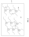
- FIG. 2 is an illustration of a sensor network 100 fabricated using stretchable silicon 105.
- the network 100 includes a plurality of components that have been fabricated on the stretchable silicon 105.
- the components include, for example, energy harvesting and storage elements 110, communication devices 120, sensors 130, and network management processors 140.
- the communications devices 120 may include both wireless and wired devices.
- the plurality of components are integrated on a medium of stretchable silicon 105, which provides multiple conductive paths 160 (interconnects) formed therein which provide, for example, conduction of electrical power from the energy harvesting and storage elements 110 to the communication devices 120, sensors 130, and network management processors 140.
- the conductive paths 160 also provide for at least some of the communication between the above listed components.
- the stretchable silicon 105 forms a portion of an autonomous network of wireless sensors.
- a high reliability results due to the redundancy built into the network 100 with stretchable silicon interconnects 160.
- the network 100 may utilize use alternative paths between the various network components to achieve reliable communications between the sensors 130 and the existing vehicle communication network.
- the illustrated network 100 has its own power source, energy harvesting and storage elements 110, the addition of such a network does not tax vehicle power systems.
- the stretchable silicon medium 105 is an excellent enabler because every node formed thereon can be converted into a component that provides a desired function. Examples include a processor function and miniature sensor nodes. In one embodiment, the nodes have a size of about 200 micrometers. In one embodiment, the stretchable silicon medium 105 is processed from a foundry-processed, monolithic silicon die, of a size between one centimeter and twenty centimeters and stretched over a larger area. The process results in a plurality of robust conductors that run between the various nodes that are fabricated on the medium 105.
- Network 100 resolves at least some of the prior problems that have been associated with weight and supportability of energy storage devices, complexity of interconnections among network nodes, manufacturability, mechanical connection of input/output signals, and scalability. More specifically, a system incorporating network 100 enables networked sensor coverage of large areas with multiple applications.
- One such application involves monitoring structural health of a structure where a plurality of the above mentioned sensors provide data to a processing element which can be queried by an external system.
- Other applications include the monitoring of air flow over aerodynamic surfaces utilizing applicable sensors fabricated on medium 105 and the monitoring of ice accretion and other hazardous conditions that may be encountered with the use of an aerospace structure.
- energy harvesting and storage elements 110 provide power to the other elements of network 100.
- a nano-piezoelectric generator effect is utilized within element 110 to convert mechanical stress into electrical current or voltage for powering the other components of network 100, including any sensors that may be fabricated on the medium 105.
- Zinc oxide (ZnO) nanowires are utilized in network 100. These ZnO nanowires are grown using chemical synthesis on a substrate with any curvature and materials nature. These ZnO nanowire generators produce power on the order of milliwatts in an area that is about one square millimeter.
- a power output associated with such energy harvesting and storage elements 110 proportionally increases as the nanowire substrate area is expanded. Also, these devices are easily integrated with stretchable silicon based nano/micro electronics devices to develop robust Nano/Micro-Electro-Mechanical Systems (N/MEMS). In certain embodiments, the energy harvesting nodes of elements 110 incorporate capacitance-based or other energy storage components to meet the energy demands of the network 100.
- At least one embodiment incorporates wireless transceiver nodes allowing data to be transmitted to and from the network 100.
- Such embodiments are referred to as single chip transceivers based on silicon systems.
- One embodiment incorporates the stretchable silicon in the fabrication of transceiver integrated circuits including the development of RF and baseband components of wireless transceivers on a single die.
- Wireless transceiver nodes can be directly connected to external devices.
- Silicon offers a high level of integration and a low cost which is desirable for large scale manufacture, and also has the potential of reducing the power consumption. Lower power consumption allows for cheaper packaging materials such as plastic which greatly reduces the cost of a chip.
- bipolar and CMOS are the most popular process technologies. Bipolar technologies offer high speed and are most commonly used in analog applications. CMOS has a lower limit frequency but offers a high level of integration which is attractive for digital applications.
- the sensor nodes 130 form a network constructed with silicon based devices.
- the sensor nodes 130 may include sensors for structural health monitoring, temperature sensors, pressure sensors, vibration sensors, ice accretion sensors, dynamic air flow separation sensors, and other sensor types.
- the sensor nodes 130 include signal conditioning circuitry, providing an interface between the sensor nodes 130 and the communications devices 120 and/or an interface between the sensor nodes and network management processors 140.
- Network management processors 140 may monitor the network for active sensor nodes 130 and determine if they belong to the network. The power required by the communications device 120, sensor nodes 130 and the network management processors 140 is supplied, in various embodiments, by the energy harvesting and storage elements 110 described above.
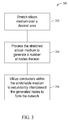
- Figure 3 is a flowchart 200 further illustrating a method for fabricating a sensor network such as those described herein incorporating stretchable silicon.
- the method illustrated in the flowchart 200 includes stretching 202 a silicon medium over a desired area, processing 204 the stretched silicon medium to generate a number of nodes thereon, and utilizing 206 conductors within the stretchable medium to redundantly interconnect the generated nodes to form the network.
- processing 204 the stretched silicon medium may include generating one or more of an energy harvesting and storage element, a communication device, a sensing device, and a processor, while utilizing 206 conductors within the stretchable medium may include routing power from energy harvesting and storage elements to the various communication devices, sensing devices, and processors.
- Processing 204 the stretched silicon medium includes generating at least one communications device with a wireless communications capability. In another embodiment, processing 204 the stretched silicon medium includes generating at least one processor capable of communicating with an external network. As further described herein, the method described by flowchart 200 is useful for multiple applications, and therefore, processing 204 the stretched silicon medium may include, but is not limited to, generating sensors for structural health monitoring and management, generating ice accretion sensors, and generating sensors configured for sensing dynamic flow separation of the air surrounding the sensor.
- the stretchable silicon substrate is capable of being stretched out, for example, up to 100 times its original size.
- such a substrate may be attached across a relevant portion of the structure.
- sensors are able to sense changes in the environment, provide data to network processors such as network management processors 140 which in turn utilize communications devices 120 to communicate the sensor data to an external system.
- network processors such as network management processors 140 which in turn utilize communications devices 120 to communicate the sensor data to an external system.
- Examples of applications outside of structural health monitoring include dynamic flow separation of the surrounding air, and the monitoring of ice accretion on structures.
- the autonomous network of wireless sensors described herein accommodates the rigorous configuration control demands of aerospace applications and enhances sensor designs and construction methods suitable for installation in hostile environments.
- a wide range of temperature sensors, pressure sensors and flow sensors for harsh and demanding environments can be utilized in aircraft and aero engines where unique applications are desired.
- the described network has the capability of incorporating advanced data systems architectures that are necessary to communicate, store and process massive amounts of health management data from large numbers of diverse sensors.
- network 100 can be configured to perform as a portion of an Integrated Vehicle Health Management (IVHM) system that will provide real-time knowledge of structural, propulsion, thermal protection and other critical systems for optimal vehicle management and mission control.
- IVHM Integrated Vehicle Health Management
- on-board, real-time sensing systems are a critical component of a vehicle health management system.
- network 100 includes sensors that have an ability to withstand harsh aerospace operating environments, while also having minimal size, weight, and power requirements.
Landscapes
- Engineering & Computer Science (AREA)
- Chemical & Material Sciences (AREA)
- Nanotechnology (AREA)
- Crystallography & Structural Chemistry (AREA)
- General Physics & Mathematics (AREA)
- Physics & Mathematics (AREA)
- Condensed Matter Physics & Semiconductors (AREA)
- Manufacturing & Machinery (AREA)
- Aviation & Aerospace Engineering (AREA)
- Computer Hardware Design (AREA)
- Microelectronics & Electronic Packaging (AREA)
- Power Engineering (AREA)
- Composite Materials (AREA)
- Materials Engineering (AREA)
- Arrangements For Transmission Of Measured Signals (AREA)
Applications Claiming Priority (2)
| Application Number | Priority Date | Filing Date | Title |
|---|---|---|---|
| US12/389,196 US7948147B2 (en) | 2009-02-19 | 2009-02-19 | Sensor network incorporating stretchable silicon |
| PCT/US2010/020301 WO2010096209A1 (en) | 2009-02-19 | 2010-01-07 | Sensor network incorporating stretchable silicon |
Publications (2)
| Publication Number | Publication Date |
|---|---|
| EP2399114A1 EP2399114A1 (en) | 2011-12-28 |
| EP2399114B1 true EP2399114B1 (en) | 2016-08-10 |
Family
ID=42060535
Family Applications (1)
| Application Number | Title | Priority Date | Filing Date |
|---|---|---|---|
| EP10701948.1A Active EP2399114B1 (en) | 2009-02-19 | 2010-01-07 | Sensor network incorporating stretchable silicon |
Country Status (5)
| Country | Link |
|---|---|
| US (2) | US7948147B2 (enExample) |
| EP (1) | EP2399114B1 (enExample) |
| JP (1) | JP5568099B2 (enExample) |
| CN (1) | CN102326064B (enExample) |
| WO (1) | WO2010096209A1 (enExample) |
Families Citing this family (8)
| Publication number | Priority date | Publication date | Assignee | Title |
|---|---|---|---|---|
| US8201773B1 (en) * | 2008-07-02 | 2012-06-19 | The United States Of America As Represented By Secretary Of The Navy | Flexible self-erecting substructures for sensor networks |
| US8510234B2 (en) * | 2010-01-05 | 2013-08-13 | American Gnc Corporation | Embedded health monitoring system based upon Optimized Neuro Genetic Fast Estimator (ONGFE) |
| FR2971054B1 (fr) * | 2011-01-31 | 2014-01-17 | Eads Europ Aeronautic Defence | Dispositif de surveillance de l'integrite et de la sante d'une structure mecanique et procede de fonctionnement d'un tel dispositif |
| WO2015037350A1 (ja) * | 2013-09-10 | 2015-03-19 | 株式会社村田製作所 | センサ |
| US10022073B2 (en) * | 2015-03-20 | 2018-07-17 | Intel Corproation | Wearable apparatus with a stretch sensor |
| US9838436B2 (en) * | 2015-03-30 | 2017-12-05 | Gulfstream Aerospace Corporation | Aircraft data networks |
| EP3839032A1 (en) | 2019-12-20 | 2021-06-23 | Imec VZW | A semiconductor cell culture device and a system for three-dimensional cell culture |
| US12492003B2 (en) | 2021-08-27 | 2025-12-09 | Goodrich Corporation | Integrated ice protection with prognostics and health management |
Citations (2)
| Publication number | Priority date | Publication date | Assignee | Title |
|---|---|---|---|---|
| JP2006089326A (ja) * | 2004-09-24 | 2006-04-06 | National Institute For Materials Science | 炭化珪素膜で被覆された硫化亜鉛ナノケーブルおよびその製造方法 |
| US20070151601A1 (en) * | 2005-12-29 | 2007-07-05 | Won Cheol Jung | Semiconductor electrode using carbon nanotube, preparation method thereof, and solar cell comprising the same |
Family Cites Families (15)
| Publication number | Priority date | Publication date | Assignee | Title |
|---|---|---|---|---|
| US4849668A (en) * | 1987-05-19 | 1989-07-18 | Massachusetts Institute Of Technology | Embedded piezoelectric structure and control |
| US5374011A (en) * | 1991-11-13 | 1994-12-20 | Massachusetts Institute Of Technology | Multivariable adaptive surface control |
| US6420819B1 (en) * | 1994-01-27 | 2002-07-16 | Active Control Experts, Inc. | Packaged strain actuator |
| US6404107B1 (en) * | 1994-01-27 | 2002-06-11 | Active Control Experts, Inc. | Packaged strain actuator |
| US6831017B1 (en) * | 2002-04-05 | 2004-12-14 | Integrated Nanosystems, Inc. | Catalyst patterning for nanowire devices |
| US6952042B2 (en) * | 2002-06-17 | 2005-10-04 | Honeywell International, Inc. | Microelectromechanical device with integrated conductive shield |
| US6870236B2 (en) * | 2003-05-20 | 2005-03-22 | Honeywell International, Inc. | Integrated resistor network for multi-functional use in constant current or constant voltage operation of a pressure sensor |
| US7231180B2 (en) * | 2004-03-24 | 2007-06-12 | Honeywell International, Inc. | Aircraft engine sensor network using wireless sensor communication modules |
| JP5031313B2 (ja) * | 2005-11-01 | 2012-09-19 | シャープ株式会社 | 外部環境ナノワイヤセンサおよび外部環境ナノワイヤセンサの製造方法 |
| US7278319B2 (en) * | 2005-11-10 | 2007-10-09 | Honeywell International Inc. | Pressure and temperature sensing element |
| US7276703B2 (en) * | 2005-11-23 | 2007-10-02 | Lockheed Martin Corporation | System to monitor the health of a structure, sensor nodes, program product, and related methods |
| US20070125176A1 (en) * | 2005-12-02 | 2007-06-07 | Honeywell International, Inc. | Energy harvesting device and methods |
| US7834424B2 (en) * | 2006-09-12 | 2010-11-16 | The Board Of Trustees Of The Leland Stanford Junior University | Extendable connector and network |
| KR20080064004A (ko) * | 2007-01-03 | 2008-07-08 | 삼성전자주식회사 | 초음파 에너지를 이용한 ZnO 나노와이어의 제조방법 |
| WO2008156606A2 (en) * | 2007-06-12 | 2008-12-24 | Adrian Pelkus | Thin film piezoelectric wave power generation system |
-
2009
- 2009-02-19 US US12/389,196 patent/US7948147B2/en active Active
-
2010
- 2010-01-07 CN CN201080008438.4A patent/CN102326064B/zh active Active
- 2010-01-07 JP JP2011551078A patent/JP5568099B2/ja active Active
- 2010-01-07 WO PCT/US2010/020301 patent/WO2010096209A1/en not_active Ceased
- 2010-01-07 EP EP10701948.1A patent/EP2399114B1/en active Active
-
2011
- 2011-04-12 US US13/084,729 patent/US8966730B1/en active Active
Patent Citations (2)
| Publication number | Priority date | Publication date | Assignee | Title |
|---|---|---|---|---|
| JP2006089326A (ja) * | 2004-09-24 | 2006-04-06 | National Institute For Materials Science | 炭化珪素膜で被覆された硫化亜鉛ナノケーブルおよびその製造方法 |
| US20070151601A1 (en) * | 2005-12-29 | 2007-07-05 | Won Cheol Jung | Semiconductor electrode using carbon nanotube, preparation method thereof, and solar cell comprising the same |
Also Published As
| Publication number | Publication date |
|---|---|
| US7948147B2 (en) | 2011-05-24 |
| US20100207487A1 (en) | 2010-08-19 |
| JP2012518183A (ja) | 2012-08-09 |
| CN102326064A (zh) | 2012-01-18 |
| WO2010096209A1 (en) | 2010-08-26 |
| EP2399114A1 (en) | 2011-12-28 |
| US8966730B1 (en) | 2015-03-03 |
| JP5568099B2 (ja) | 2014-08-06 |
| CN102326064B (zh) | 2014-10-15 |
Similar Documents
| Publication | Publication Date | Title |
|---|---|---|
| EP2399114B1 (en) | Sensor network incorporating stretchable silicon | |
| Yang et al. | Review of flexible microelectromechanical system sensors and devices | |
| US7301454B2 (en) | Sensor system | |
| Ko | The future of sensor and actuator systems | |
| Yuan et al. | Recent progress on distributed structural health monitoring research at NUAA | |
| JP2012518183A5 (enExample) | ||
| Sundriyal et al. | Energy harvesting techniques for powering wireless sensor networks in aircraft applications: A review | |
| JP5145522B2 (ja) | 遠隔監視システム | |
| CN107727283A (zh) | 一种机器人皮肤触感系统及实现方法 | |
| CN102085918A (zh) | 星上挠性振动的二元智能结构控制装置 | |
| Hadas et al. | Development of energy harvesting sources for remote applications as mechatronic systems | |
| Nakad et al. | Communications in electronic textile systems | |
| Lynch et al. | A wireless inertial measurement system (WIMS) for an interactive dance environment | |
| Hunter et al. | A brief review of the need for robust smart wireless sensor systems for future propulsion systems, distributed engine controls, and propulsion health management | |
| Kumar et al. | Energy Harvesting–Based Architecture in IoT: Basics of Energy Harvesting, Key Technology for Enhancing the Life of IoT Devices, Challenges of IoT in Terms of Energy and Power Consumption | |
| Janak et al. | Energy harvesting for aerospace: Application possibilities | |
| Suster et al. | Optically-powered wireless transmitter for high-temperature MEMS sensing and communication | |
| Eteng | Sensors, actuators, wireless sensor networks, and the Internet of Things | |
| CN107037811A (zh) | 微纳航天器集群飞行控制系统及方法 | |
| Gomathi et al. | An efficient and effective energy harvesting system using surface micromachined accelerometer | |
| Maenaka | Sensors in Network (3)—What and How Data Should Be Networked?— | |
| Gatti et al. | Building Autonomous IIoT Networks Using Energy Harvesters | |
| CN109302099A (zh) | 一种基于桥架式mpeg和mteg的太阳能与振动能多能互补的微型自供能装置 | |
| CN214627378U (zh) | 共烧陶瓷型传感器和传感器网络 | |
| Baysal et al. | Direct Ink Writing of PEDOT: PSS Aerogel for Flexible and Performing Thermoelectrics |
Legal Events
| Date | Code | Title | Description |
|---|---|---|---|
| PUAI | Public reference made under article 153(3) epc to a published international application that has entered the european phase |
Free format text: ORIGINAL CODE: 0009012 |
|
| 17P | Request for examination filed |
Effective date: 20110830 |
|
| AK | Designated contracting states |
Kind code of ref document: A1 Designated state(s): AT BE BG CH CY CZ DE DK EE ES FI FR GB GR HR HU IE IS IT LI LT LU LV MC MK MT NL NO PL PT RO SE SI SK SM TR |
|
| DAX | Request for extension of the european patent (deleted) | ||
| 17Q | First examination report despatched |
Effective date: 20150603 |
|
| RIC1 | Information provided on ipc code assigned before grant |
Ipc: B82Y 10/00 20110101ALI20151029BHEP Ipc: G01M 5/00 20060101AFI20151029BHEP Ipc: H01L 21/02 20060101ALI20151029BHEP Ipc: B82Y 40/00 20110101ALI20151029BHEP Ipc: B82B 3/00 20060101ALI20151029BHEP Ipc: H01L 41/04 20060101ALI20151029BHEP Ipc: B82Y 30/00 20110101ALI20151029BHEP Ipc: H01L 41/08 20060101ALI20151029BHEP |
|
| GRAP | Despatch of communication of intention to grant a patent |
Free format text: ORIGINAL CODE: EPIDOSNIGR1 |
|
| INTG | Intention to grant announced |
Effective date: 20151222 |
|
| INTG | Intention to grant announced |
Effective date: 20160223 |
|
| GRAS | Grant fee paid |
Free format text: ORIGINAL CODE: EPIDOSNIGR3 |
|
| GRAA | (expected) grant |
Free format text: ORIGINAL CODE: 0009210 |
|
| AK | Designated contracting states |
Kind code of ref document: B1 Designated state(s): AT BE BG CH CY CZ DE DK EE ES FI FR GB GR HR HU IE IS IT LI LT LU LV MC MK MT NL NO PL PT RO SE SI SK SM TR |
|
| REG | Reference to a national code |
Ref country code: GB Ref legal event code: FG4D |
|
| REG | Reference to a national code |
Ref country code: CH Ref legal event code: EP Ref country code: AT Ref legal event code: REF Ref document number: 819497 Country of ref document: AT Kind code of ref document: T Effective date: 20160815 |
|
| REG | Reference to a national code |
Ref country code: IE Ref legal event code: FG4D |
|
| REG | Reference to a national code |
Ref country code: DE Ref legal event code: R096 Ref document number: 602010035321 Country of ref document: DE |
|
| REG | Reference to a national code |
Ref country code: LT Ref legal event code: MG4D |
|
| REG | Reference to a national code |
Ref country code: NL Ref legal event code: MP Effective date: 20160810 |
|
| REG | Reference to a national code |
Ref country code: AT Ref legal event code: MK05 Ref document number: 819497 Country of ref document: AT Kind code of ref document: T Effective date: 20160810 |
|
| REG | Reference to a national code |
Ref country code: FR Ref legal event code: PLFP Year of fee payment: 8 |
|
| PG25 | Lapsed in a contracting state [announced via postgrant information from national office to epo] |
Ref country code: NO Free format text: LAPSE BECAUSE OF FAILURE TO SUBMIT A TRANSLATION OF THE DESCRIPTION OR TO PAY THE FEE WITHIN THE PRESCRIBED TIME-LIMIT Effective date: 20161110 Ref country code: HR Free format text: LAPSE BECAUSE OF FAILURE TO SUBMIT A TRANSLATION OF THE DESCRIPTION OR TO PAY THE FEE WITHIN THE PRESCRIBED TIME-LIMIT Effective date: 20160810 Ref country code: FI Free format text: LAPSE BECAUSE OF FAILURE TO SUBMIT A TRANSLATION OF THE DESCRIPTION OR TO PAY THE FEE WITHIN THE PRESCRIBED TIME-LIMIT Effective date: 20160810 Ref country code: IT Free format text: LAPSE BECAUSE OF FAILURE TO SUBMIT A TRANSLATION OF THE DESCRIPTION OR TO PAY THE FEE WITHIN THE PRESCRIBED TIME-LIMIT Effective date: 20160810 Ref country code: NL Free format text: LAPSE BECAUSE OF FAILURE TO SUBMIT A TRANSLATION OF THE DESCRIPTION OR TO PAY THE FEE WITHIN THE PRESCRIBED TIME-LIMIT Effective date: 20160810 Ref country code: IS Free format text: LAPSE BECAUSE OF FAILURE TO SUBMIT A TRANSLATION OF THE DESCRIPTION OR TO PAY THE FEE WITHIN THE PRESCRIBED TIME-LIMIT Effective date: 20161210 Ref country code: LT Free format text: LAPSE BECAUSE OF FAILURE TO SUBMIT A TRANSLATION OF THE DESCRIPTION OR TO PAY THE FEE WITHIN THE PRESCRIBED TIME-LIMIT Effective date: 20160810 |
|
| PG25 | Lapsed in a contracting state [announced via postgrant information from national office to epo] |
Ref country code: LV Free format text: LAPSE BECAUSE OF FAILURE TO SUBMIT A TRANSLATION OF THE DESCRIPTION OR TO PAY THE FEE WITHIN THE PRESCRIBED TIME-LIMIT Effective date: 20160810 Ref country code: AT Free format text: LAPSE BECAUSE OF FAILURE TO SUBMIT A TRANSLATION OF THE DESCRIPTION OR TO PAY THE FEE WITHIN THE PRESCRIBED TIME-LIMIT Effective date: 20160810 Ref country code: PL Free format text: LAPSE BECAUSE OF FAILURE TO SUBMIT A TRANSLATION OF THE DESCRIPTION OR TO PAY THE FEE WITHIN THE PRESCRIBED TIME-LIMIT Effective date: 20160810 Ref country code: GR Free format text: LAPSE BECAUSE OF FAILURE TO SUBMIT A TRANSLATION OF THE DESCRIPTION OR TO PAY THE FEE WITHIN THE PRESCRIBED TIME-LIMIT Effective date: 20161111 Ref country code: PT Free format text: LAPSE BECAUSE OF FAILURE TO SUBMIT A TRANSLATION OF THE DESCRIPTION OR TO PAY THE FEE WITHIN THE PRESCRIBED TIME-LIMIT Effective date: 20161212 Ref country code: SE Free format text: LAPSE BECAUSE OF FAILURE TO SUBMIT A TRANSLATION OF THE DESCRIPTION OR TO PAY THE FEE WITHIN THE PRESCRIBED TIME-LIMIT Effective date: 20160810 Ref country code: ES Free format text: LAPSE BECAUSE OF FAILURE TO SUBMIT A TRANSLATION OF THE DESCRIPTION OR TO PAY THE FEE WITHIN THE PRESCRIBED TIME-LIMIT Effective date: 20160810 |
|
| PG25 | Lapsed in a contracting state [announced via postgrant information from national office to epo] |
Ref country code: RO Free format text: LAPSE BECAUSE OF FAILURE TO SUBMIT A TRANSLATION OF THE DESCRIPTION OR TO PAY THE FEE WITHIN THE PRESCRIBED TIME-LIMIT Effective date: 20160810 Ref country code: EE Free format text: LAPSE BECAUSE OF FAILURE TO SUBMIT A TRANSLATION OF THE DESCRIPTION OR TO PAY THE FEE WITHIN THE PRESCRIBED TIME-LIMIT Effective date: 20160810 |
|
| REG | Reference to a national code |
Ref country code: DE Ref legal event code: R097 Ref document number: 602010035321 Country of ref document: DE |
|
| PG25 | Lapsed in a contracting state [announced via postgrant information from national office to epo] |
Ref country code: BG Free format text: LAPSE BECAUSE OF FAILURE TO SUBMIT A TRANSLATION OF THE DESCRIPTION OR TO PAY THE FEE WITHIN THE PRESCRIBED TIME-LIMIT Effective date: 20161110 Ref country code: SM Free format text: LAPSE BECAUSE OF FAILURE TO SUBMIT A TRANSLATION OF THE DESCRIPTION OR TO PAY THE FEE WITHIN THE PRESCRIBED TIME-LIMIT Effective date: 20160810 Ref country code: BE Free format text: LAPSE BECAUSE OF FAILURE TO SUBMIT A TRANSLATION OF THE DESCRIPTION OR TO PAY THE FEE WITHIN THE PRESCRIBED TIME-LIMIT Effective date: 20160810 Ref country code: SK Free format text: LAPSE BECAUSE OF FAILURE TO SUBMIT A TRANSLATION OF THE DESCRIPTION OR TO PAY THE FEE WITHIN THE PRESCRIBED TIME-LIMIT Effective date: 20160810 Ref country code: DK Free format text: LAPSE BECAUSE OF FAILURE TO SUBMIT A TRANSLATION OF THE DESCRIPTION OR TO PAY THE FEE WITHIN THE PRESCRIBED TIME-LIMIT Effective date: 20160810 Ref country code: CZ Free format text: LAPSE BECAUSE OF FAILURE TO SUBMIT A TRANSLATION OF THE DESCRIPTION OR TO PAY THE FEE WITHIN THE PRESCRIBED TIME-LIMIT Effective date: 20160810 |
|
| PLBE | No opposition filed within time limit |
Free format text: ORIGINAL CODE: 0009261 |
|
| STAA | Information on the status of an ep patent application or granted ep patent |
Free format text: STATUS: NO OPPOSITION FILED WITHIN TIME LIMIT |
|
| 26N | No opposition filed |
Effective date: 20170511 |
|
| PG25 | Lapsed in a contracting state [announced via postgrant information from national office to epo] |
Ref country code: SI Free format text: LAPSE BECAUSE OF FAILURE TO SUBMIT A TRANSLATION OF THE DESCRIPTION OR TO PAY THE FEE WITHIN THE PRESCRIBED TIME-LIMIT Effective date: 20160810 |
|
| REG | Reference to a national code |
Ref country code: CH Ref legal event code: PL |
|
| PG25 | Lapsed in a contracting state [announced via postgrant information from national office to epo] |
Ref country code: MC Free format text: LAPSE BECAUSE OF FAILURE TO SUBMIT A TRANSLATION OF THE DESCRIPTION OR TO PAY THE FEE WITHIN THE PRESCRIBED TIME-LIMIT Effective date: 20160810 |
|
| PG25 | Lapsed in a contracting state [announced via postgrant information from national office to epo] |
Ref country code: CH Free format text: LAPSE BECAUSE OF NON-PAYMENT OF DUE FEES Effective date: 20170131 Ref country code: LI Free format text: LAPSE BECAUSE OF NON-PAYMENT OF DUE FEES Effective date: 20170131 |
|
| REG | Reference to a national code |
Ref country code: IE Ref legal event code: MM4A |
|
| PG25 | Lapsed in a contracting state [announced via postgrant information from national office to epo] |
Ref country code: LU Free format text: LAPSE BECAUSE OF NON-PAYMENT OF DUE FEES Effective date: 20170107 |
|
| REG | Reference to a national code |
Ref country code: FR Ref legal event code: PLFP Year of fee payment: 9 |
|
| PG25 | Lapsed in a contracting state [announced via postgrant information from national office to epo] |
Ref country code: IE Free format text: LAPSE BECAUSE OF NON-PAYMENT OF DUE FEES Effective date: 20170107 |
|
| PG25 | Lapsed in a contracting state [announced via postgrant information from national office to epo] |
Ref country code: MT Free format text: LAPSE BECAUSE OF NON-PAYMENT OF DUE FEES Effective date: 20170107 |
|
| PG25 | Lapsed in a contracting state [announced via postgrant information from national office to epo] |
Ref country code: HU Free format text: LAPSE BECAUSE OF FAILURE TO SUBMIT A TRANSLATION OF THE DESCRIPTION OR TO PAY THE FEE WITHIN THE PRESCRIBED TIME-LIMIT; INVALID AB INITIO Effective date: 20100107 |
|
| PG25 | Lapsed in a contracting state [announced via postgrant information from national office to epo] |
Ref country code: CY Free format text: LAPSE BECAUSE OF NON-PAYMENT OF DUE FEES Effective date: 20160810 |
|
| PG25 | Lapsed in a contracting state [announced via postgrant information from national office to epo] |
Ref country code: MK Free format text: LAPSE BECAUSE OF FAILURE TO SUBMIT A TRANSLATION OF THE DESCRIPTION OR TO PAY THE FEE WITHIN THE PRESCRIBED TIME-LIMIT Effective date: 20160810 |
|
| PG25 | Lapsed in a contracting state [announced via postgrant information from national office to epo] |
Ref country code: TR Free format text: LAPSE BECAUSE OF FAILURE TO SUBMIT A TRANSLATION OF THE DESCRIPTION OR TO PAY THE FEE WITHIN THE PRESCRIBED TIME-LIMIT Effective date: 20160810 |
|
| P01 | Opt-out of the competence of the unified patent court (upc) registered |
Effective date: 20230516 |
|
| PGFP | Annual fee paid to national office [announced via postgrant information from national office to epo] |
Ref country code: DE Payment date: 20250129 Year of fee payment: 16 |
|
| PGFP | Annual fee paid to national office [announced via postgrant information from national office to epo] |
Ref country code: FR Payment date: 20250127 Year of fee payment: 16 |
|
| PGFP | Annual fee paid to national office [announced via postgrant information from national office to epo] |
Ref country code: GB Payment date: 20250127 Year of fee payment: 16 |