EP2397580A2 - Verfahren und Vorrichtung zur Herstellung eines Silicium-Substrats mit ausgezeichneter Oberflächenqualität mittels Intertgasblasverfahren - Google Patents
Verfahren und Vorrichtung zur Herstellung eines Silicium-Substrats mit ausgezeichneter Oberflächenqualität mittels Intertgasblasverfahren Download PDFInfo
- Publication number
- EP2397580A2 EP2397580A2 EP11169731A EP11169731A EP2397580A2 EP 2397580 A2 EP2397580 A2 EP 2397580A2 EP 11169731 A EP11169731 A EP 11169731A EP 11169731 A EP11169731 A EP 11169731A EP 2397580 A2 EP2397580 A2 EP 2397580A2
- Authority
- EP
- European Patent Office
- Prior art keywords
- silicon
- molten
- unit
- molten silicon
- melting
- Prior art date
- Legal status (The legal status is an assumption and is not a legal conclusion. Google has not performed a legal analysis and makes no representation as to the accuracy of the status listed.)
- Granted
Links
Images



Classifications
-
- C—CHEMISTRY; METALLURGY
- C30—CRYSTAL GROWTH
- C30B—SINGLE-CRYSTAL GROWTH; UNIDIRECTIONAL SOLIDIFICATION OF EUTECTIC MATERIAL OR UNIDIRECTIONAL DEMIXING OF EUTECTOID MATERIAL; REFINING BY ZONE-MELTING OF MATERIAL; PRODUCTION OF A HOMOGENEOUS POLYCRYSTALLINE MATERIAL WITH DEFINED STRUCTURE; SINGLE CRYSTALS OR HOMOGENEOUS POLYCRYSTALLINE MATERIAL WITH DEFINED STRUCTURE; AFTER-TREATMENT OF SINGLE CRYSTALS OR A HOMOGENEOUS POLYCRYSTALLINE MATERIAL WITH DEFINED STRUCTURE; APPARATUS THEREFOR
- C30B15/00—Single-crystal growth by pulling from a melt, e.g. Czochralski method
- C30B15/007—Pulling on a substrate
-
- C—CHEMISTRY; METALLURGY
- C30—CRYSTAL GROWTH
- C30B—SINGLE-CRYSTAL GROWTH; UNIDIRECTIONAL SOLIDIFICATION OF EUTECTIC MATERIAL OR UNIDIRECTIONAL DEMIXING OF EUTECTOID MATERIAL; REFINING BY ZONE-MELTING OF MATERIAL; PRODUCTION OF A HOMOGENEOUS POLYCRYSTALLINE MATERIAL WITH DEFINED STRUCTURE; SINGLE CRYSTALS OR HOMOGENEOUS POLYCRYSTALLINE MATERIAL WITH DEFINED STRUCTURE; AFTER-TREATMENT OF SINGLE CRYSTALS OR A HOMOGENEOUS POLYCRYSTALLINE MATERIAL WITH DEFINED STRUCTURE; APPARATUS THEREFOR
- C30B15/00—Single-crystal growth by pulling from a melt, e.g. Czochralski method
- C30B15/06—Non-vertical pulling
-
- C—CHEMISTRY; METALLURGY
- C30—CRYSTAL GROWTH
- C30B—SINGLE-CRYSTAL GROWTH; UNIDIRECTIONAL SOLIDIFICATION OF EUTECTIC MATERIAL OR UNIDIRECTIONAL DEMIXING OF EUTECTOID MATERIAL; REFINING BY ZONE-MELTING OF MATERIAL; PRODUCTION OF A HOMOGENEOUS POLYCRYSTALLINE MATERIAL WITH DEFINED STRUCTURE; SINGLE CRYSTALS OR HOMOGENEOUS POLYCRYSTALLINE MATERIAL WITH DEFINED STRUCTURE; AFTER-TREATMENT OF SINGLE CRYSTALS OR A HOMOGENEOUS POLYCRYSTALLINE MATERIAL WITH DEFINED STRUCTURE; APPARATUS THEREFOR
- C30B15/00—Single-crystal growth by pulling from a melt, e.g. Czochralski method
- C30B15/14—Heating of the melt or the crystallised materials
-
- C—CHEMISTRY; METALLURGY
- C30—CRYSTAL GROWTH
- C30B—SINGLE-CRYSTAL GROWTH; UNIDIRECTIONAL SOLIDIFICATION OF EUTECTIC MATERIAL OR UNIDIRECTIONAL DEMIXING OF EUTECTOID MATERIAL; REFINING BY ZONE-MELTING OF MATERIAL; PRODUCTION OF A HOMOGENEOUS POLYCRYSTALLINE MATERIAL WITH DEFINED STRUCTURE; SINGLE CRYSTALS OR HOMOGENEOUS POLYCRYSTALLINE MATERIAL WITH DEFINED STRUCTURE; AFTER-TREATMENT OF SINGLE CRYSTALS OR A HOMOGENEOUS POLYCRYSTALLINE MATERIAL WITH DEFINED STRUCTURE; APPARATUS THEREFOR
- C30B29/00—Single crystals or homogeneous polycrystalline material with defined structure characterised by the material or by their shape
- C30B29/02—Elements
- C30B29/06—Silicon
Definitions
- the present invention relates to a technique for manufacturing a silicon substrate and, more particularly, to a method and apparatus for manufacturing a silicon substrate using inert gas blowing during continuous casting to provide excellent productivity and surface quality.
- a silicon substrate is a main component of a silicon solar cell and constitutes about 28% of the price of a solar cell module.
- a silicon substrate for solar cells is manufactured by melting raw silicon and solidifying molten silicon to prepare a single crystalline silicon ingot or polycrystalline silicon block, which in turn is subjected to several cutting processes.
- a technique for directly manufacturing a silicon substrate from molten silicon can be classified into a vertical growth type and a horizontal growth type.
- the vertical growth technique has already been used in the art but has a problem of low growth speed.
- the horizontal growth technique is not used in the art, despite high growth speed.
- a ribbon growth on substrate (RGS) process is representatively used.
- RGS ribbon growth on substrate
- solidification of molten silicon is controlled in a molten silicon container and shape control is performed using a blade, thereby causing the following problems.
- the RGS process employs the blade for shape control of the substrate.
- there is a high possibility of blade failure and mechanical contact between the blade and the silicon substrate is likely to cause contamination of the substrate.
- One aspect of the invention is to provide an apparatus for manufacturing a silicon substrate, which can directly manufacture a silicon substrate from molten silicon using inert gas blowing during continuous casting to improve surface quality of the silicon substrate.
- Another aspect of the invention is to provide a silicon substrate manufacturing method which can improve surface quality of a silicon substrate using inert gas blowing.
- an apparatus for manufacturing a silicon substrate using inert gas blowing which provides excellent surface quality.
- the apparatus includes a raw silicon feeder through which raw silicon is fed; a silicon melting unit disposed under the raw silicon feeder and melting the raw silicon to form molten silicon; a molten silicon storage unit storing the molten silicon supplied from the silicon melting unit and tapping the molten silicon to provide a silicon melt having a constant thickness; a transfer unit transferring the silicon melt tapped from the molten silicon storage unit; and a cooling unit cooling the silicon melt transferred by the transfer unit.
- the cooling unit cools the silicon melt by blowing inert gas at a rate of 0.1 ⁇ 3 Nm 3 /h.
- a method of manufacturing a silicon substrate using inert gas blowing which provides excellent surface quality.
- the method includes: (a) supplying raw silicon into the silicon melting unit; (b) melting the raw silicon placed in the silicon melting unit to form molten silicon; (c) opening a gate of the silicon melting unit to tap the molten silicon; (d) storing the tapped molten silicon in the molten silicon storage unit; (e) driving the transfer unit to eject the molten silicon; and (f) cooling the molten silicon by blowing inert gas to the molten silicon transferred by the transfer unit.
- the inert gas is blown at a rate of 0.1 ⁇ 3 Nm 3 /h.
- Fig. 1 is a schematic view of an apparatus for manufacturing a silicon substrate using inert gas blowing according to one exemplary embodiment of the present invention.
- the apparatus 100 for manufacturing a silicon substrate includes a raw silicon feeder 110, a silicon melting unit 120, a molten silicon storage unit 130, a transfer unit 140, and a cooling unit 150.
- the raw silicon feeder 110 receives raw silicon from outside and supplies a predetermined amount of raw silicon into the silicon melting unit 120.
- the silicon melting unit 120 melts the supplied raw silicon to form molten silicon.
- the silicon melting unit 120 may melt the raw silicon using various heating manners such as induction heating, resistance heating, and the like.
- induction heating will be described as an example of a process for melting raw silicon.
- silicon is difficult to apply direct heating through electromagnetic induction due to low electrical conductivity of silicon at a temperature of about 700°C or less.
- raw silicon can be melted through indirect melting in a crucible.
- a graphite crucible For silicon melting through indirect melting, a graphite crucible may be used. Although graphite is non-metallic, excellent electrical and thermal conductivity of graphite facilitate heating of the raw silicon through electromagnetic induction.
- silicon when silicon is indirectly melted by heat in the graphite crucible, there is a problem of contamination of silicon or an inner surface of the crucible.
- the raw silicon be subjected to indirect melting using crucible heat at a temperature of 700°C or less and subjected to non-contact melting through induction melting at a temperature exceeding 700°C to minimize the problem of contamination of the silicon.
- the silicon melting unit 120 may be an induction melting device that includes a crucible 121, an induction coil 122, a tapping hole 123, and a gate 124.
- the crucible 121 receives the raw silicon from the feeder and has the tapping hole 123 formed at a lower side thereof.
- the crucible 121 may be a graphite crucible or a water-cooled crucible. Alternatively, a combination of the graphite crucible and the water-cooled crucible may be used as the crucible 121.
- the induction coil 122 is wound around an outer wall of the crucible 121.
- the induction coil 122 is connected to an AC power source.
- the gate 124 opens or closes the tapping hole 123 formed at the lower side of the crucible 121.
- the gate 124 may be a bar type gate, but is not limited thereto. Alternatively, the gate 124 may be a valve type gate.
- the molten silicon storage unit 130 stores the molten silicon supplied from the silicon melting unit 120 and taps the molten silicon to provide a silicon melt having a constant thickness.
- the molten silicon storage unit 130 may be open at a lower side thereof. In this case, the transfer unit 40 disposed at the lower side of the molten silicon storage unit 130 defines the lower side of the molten silicon storage unit 130.
- the molten silicon storage unit 130 is formed at one side of a lower portion thereof with an ejection port 132 through which the molten silicon is ejected.
- the thickness of the ejection port 132 may act as a factor determining the thickness of a silicon substrate and may be in the range of about 0.1 ⁇ 2 mm.
- the transfer unit 140 is disposed at the lower side of the molten silicon storage unit 130 and continuously transfers the silicon melt ejected from the molten silicon storage unit 130.
- the transfer unit 140 may be a transfer board and employ a conveyer belt type transfer device.
- the transfer unit 140 When the transfer unit 140 is a transfer board, the transfer unit may be constituted by a single board or may be divided into a transfer board which is responsible for transferring the molten silicon and a lower substrate which contacts the molten silicon and forms the silicon substrate.
- the transfer unit 140 may be pre-heated by a preheating unit 142 to minimize temperature difference between the silicon melt and the transfer unit.
- the transfer unit 140 may be made of a material, such as C, SiC, Si 3 N 4 , graphite, Al 2 O 3 and Mo, which have different coefficients of thermal expansion than silicon. As the transfer unit 140 has a different coefficient of thermal expansion than silicon, the silicon substrate can be easily separated from the transfer unit 140 when manufactured by cooling the silicon melt, and the transfer unit 140 can be reused.
- the cooling unit 150 cools the silicon melt to form the silicon substrate.
- the cooling unit 150 cools the silicon melt by blowing an inert gas such as argon, helium, nitrogen, and the like.
- the inert gas may be at least one selected from the group of argon, helium, nitrogen, and mixtures thereof.
- Inert gas blowing may assist in removal of the remaining melt which can be formed by rapid cooling of the silicon melt and is performed to facilitate control of the surface shape of a silicon substrate manufactured through surface flattening.
- the inert gas may by blown at a rate of 0.1 ⁇ 3 Nm 3 /h. More preferably, the inert gas is blown at a rate of 0.6 ⁇ 2.5 Nm 3 /h. If the inert gas is blown at a rate less than 0.1 1 Nm 3 /h, the silicon substrate can be excessively thickened due to inefficient inert gas blowing, thereby making it impossible to perform continuous casting. On the other hand, if the inert gas is blown at a rate exceeding 3 Nm 3 /h, the silicon melt is blown, thereby making it impossible to obtain continuous manufacture of the silicon substrate.
- productivity and quality of the manufactured silicon substrate can be significantly affected by process variables, such as the surface temperature of the molten silicon, the preheating temperature of the transfer unit, and the moving speed of the transfer unit. These process variables affect productivity of the silicon substrate through combinational influence rather than individual influence.
- the process variables may be adjusted such that the surface temperature of the molten silicon is in the range of 1350 ⁇ 1500°C, the preheating temperature of the transfer unit is in the range of 750 ⁇ 1400°C, and the moving speed of the transfer unit 140 is in the range of 450 ⁇ 1400 cm/min. Further, the transfer time of the silicon substrate after tapping the molten silicon from the molten silicon storage unit may be in the range of 0.5 ⁇ 3.5 seconds.
- the molten silicon can solidify before tapping. If the surface temperature of the molten silicon exceeds 1500°C, the silicon melt can trickle down during transfer of the tapped silicon melt.
- the molten silicon can solidify at a contact portion between the transfer unit 140 and the molten silicon.
- the preheating temperature of the transfer unit 140 exceeds 1400°C, the silicon melt can trickle down.
- the moving speed of the transfer unit 140 is less than 450 cm/min, the manufactured silicon substrate can be excessively thickened. On the contrary, if the moving speed of the transfer unit 140 exceeds 1400 cm/min, the manufactured silicon substrate can be excessively thinned.
- the transfer time of the silicon substrate after tapping the molten silicon from the molten silicon storage unit is less than 0.5 seconds, the manufactured silicon substrate can be excessively thinned. On the contrary, if the transfer time of the silicon substrate after tapping exceeds 3.5 seconds, the silicon substrate can be excessively thickened, thereby making it impossible to perform continuous casting.
- Fig. 2 is a flowchart of a method of manufacturing a silicon substrate using inert gas blowing according to one exemplary embodiment of the present invention.
- the silicon substrate manufacturing method using inert gas blowing includes preheating a transfer unit in S210, supplying raw silicon in S220, forming molten silicon in S230, opening a gate in S240, storing the molten silicon in S250, ejecting the molten silicon in S260, and cooling a silicon melt in S270.
- the transfer unit disposed at one side of a lower portion of a molten silicon storage unit is preheated.
- the preheating temperature of the transfer unit may be in the range of 750 ⁇ 1400°C. If the preheating temperature of the transfer unit is less than 750°C, the molten silicon can be solidified at a contact portion between the transfer unit and the molten silicon. On the contrary, if the preheating temperature of the transfer unit exceeds 1400°C, the silicon melt can trickle down.
- the transfer unit may be made of a material that has good wettability, high corrosion resistance and a higher melting point than that of silicon. Further, in order to guarantee easy separation of the silicon substrate after cooling, the transfer unit may be made of a material having a different coefficient of thermal expansion than silicon. Specifically, the transfer unit may be made of at least one material selected from C, SiC, Si 3 N 4 , graphite, Al 2 O 3 and Mo.
- Operation S210 of preheating the transfer unit may be performed before operation S240 of opening the gate or operation S250 of storing the molten silicon.
- preheating of the transfer unit is not necessarily performed at an initial stage of the method and may be performed by various selective methods as needed.
- a predetermined amount of raw silicon is supplied into a silicon melting unit through a raw silicon feeder.
- the raw silicon placed in the silicon melting unit is melted to form molten silicon.
- the raw silicon may be melted through induction melting.
- the silicon melting unit may include a crucible that receives the raw silicon and has a tapping hole formed at a lower side thereof, an induction coil wound around an outer wall of the crucible, and a gate opening or closing the tapping hole.
- the gate is opened to tap the molten silicon from the silicon melting unit.
- the molten silicon tapped from the silicon melting unit is stored.
- the surface temperature of the molten silicon may be kept in the range of 1350 ⁇ 1500°C. If the surface temperature of the molten silicon stored in the molten silicon storage unit is less than 1350°C, the molten silicon can solidify before tapping. If the surface temperature of the molten silicon exceeds 1500°C, the silicon melt can trickle down during transfer of the tapped silicon melt.
- the transfer unit In operation S260 of ejecting the molten silicon, the transfer unit is driven in the horizontal direction to eject the molten silicon through an ejection port.
- the moving speed of the transfer unit may be in the range of 450 ⁇ 1400 cm/min, and the transfer time of the silicon substrate after tapping the molten silicon from the molten silicon storage unit may be in the range of 0.5 ⁇ 3.5 seconds.
- the moving speed of the transfer unit is less than 450 cm/min, the manufactured silicon substrate can be excessively thickened. If the moving speed of the transfer unit exceeds 1400 cm/min, the manufactured silicon substrate can be excessively thinned.
- the transfer time of the silicon substrate after tapping the molten silicon from the molten silicon storage unit is less than 0.5 seconds, the manufactured silicon substrate can be excessively thinned. If the transfer time of the silicon substrate after tapping exceeds 3.5 seconds, the silicon substrate can be excessively thickened, thereby making it impossible to perform continuous casting.
- cooling the silicon melt may be performed by inert gas blowing, and the inert gas may be argon, without being limited thereto.
- the inert gas blowing may be performed using helium, nitrogen, and the like.
- the inert gas may by blown at a rate of 0.1 ⁇ 3 Nm 3 /h. More preferably, the inert gas is blown at a rate of 0.6 ⁇ 2.5 Nm 3 /h. If the inert gas is blown at a rate less than 0.1 Nm 3 /h, the silicon substrate can be excessively thickened due to inefficient inert gas blowing, thereby making it impossible to perform continuous casting. On the other hand, if the inert gas is blown at a rate exceeding 3 Nm 3 /h, the silicon melt is blown, thereby making it impossible to obtain continuous manufacture of the silicon substrate.
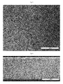
- Fig. 3 is a micrograph showing the microstructure of a surface of a silicon substrate manufactured by the apparatus according to the exemplary embodiment and Fig. 4 is a micrograph showing the microstructure of a cross-section of the silicon substrate of Fig. 3 .
- the manufactured silicon substrate has a polycrystalline structure, an average grain size of 50-100 ⁇ m, and a vertically grown columnar structure.
- the silicon substrate having such a columnar structure is used for a solar cell, minor carriers excited by sunlight have increased lifetime, thereby improving cell efficiency.
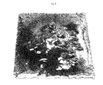
- Fig. 5 is a picture showing the surface of a silicon substrate manufactured without application of inert gas blowing
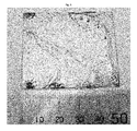
- Fig. 6 is a picture showing the surface of a silicon substrate manufactured using inert gas blowing.
- the silicon substrate when the silicon melt is not subjected to inert gas blowing, the silicon substrate has a rough surface.
- Silicon has a melt density of about 2.57 g/cm 3 and a solid density of about 2.33 g/cm 3 . Since the solid density of silicon is lower than the melt density, silicon undergoes expansion during solidification and can have a rough surface in the case where the silicon undergoes non-uniform expansion, as shown in Fig. 5 . As a result, the manufactured silicon substrate has low surface quality.
- the manufactured silicon substrate has excellent surface quality as compared to that shown in Fig. 5 .
- Fig. 7 is a picture showing a polished surface of the silicon substrate of Fig. 6 .
- the substrate for solar cells typically has a thickness of 100-400 ⁇ m. Accordingly, when the silicon substrate manufactured by the method shown in Fig. 7 is adjusted to have a thickness of 100-400 ⁇ m, the silicon substrate may be used for solar cells.
- the apparatus and method according to the embodiments of the invention may improve productivity of a silicon substrate through inert gas blowing during continuous casting, which has excellent productivity and facilitates property control.
- the silicon substrate manufactured using the apparatus and method according to the embodiments has excellent surface quality to be suited for solar cells.
- Table 1 shows the thicknesses and shapes of silicon substrates prepared by conditions of Examples 1 to 4 and Comparative Example 1.
- Table 1 Preheating temperature (°C) Moving speed (cm/min) Transfer time after tapping (second) Blowing rate of argon (Nm 3 /h) Substrate thickness ( ⁇ m) Substrate shape Example 1 1,000 485 2 5 0 5 852 Bad Example 2 1,000 485 2 5 0 65 320 Good Example 3 1,000 485 2 5 0 8 278 Good Example 4 1,000 485 2 5 1 1 258 Good Comparative 1,000 485 2 5 3 0 - Bad example 1
- Examples 1 to 4 were prepared to determine a relationship between the thickness and shape of the manufactured substrate and the blowing amount of argon. In Examples 1 to 4, it was ascertained that the thickness of the substrate decreased with increasing blowing rate of argon.
- Example 1 it could be seen from Example 1 that the silicon substrate was excessively thickened due to inefficient inert gas blowing when the blowing rate of argon was 0.5 Nm 3 /h, and that a desired effect of inert gas blowing was obtained from a blowing rate of argon of 0.65 Nm 3 /h or more.
Landscapes
- Chemical & Material Sciences (AREA)
- Engineering & Computer Science (AREA)
- Crystallography & Structural Chemistry (AREA)
- Materials Engineering (AREA)
- Metallurgy (AREA)
- Organic Chemistry (AREA)
- Silicon Compounds (AREA)
Applications Claiming Priority (2)
| Application Number | Priority Date | Filing Date | Title |
|---|---|---|---|
| KR1020100055949A KR101111408B1 (ko) | 2010-06-14 | 2010-06-14 | 불활성 가스 블로윙을 이용한 실리콘 박판 제조 장치 |
| KR1020110056067A KR101248073B1 (ko) | 2011-06-10 | 2011-06-10 | 불활성 가스 블로윙을 이용한 표면 품질이 우수한 실리콘 기판 제조 장치 및 그 제조 방법 |
Publications (3)
| Publication Number | Publication Date |
|---|---|
| EP2397580A2 true EP2397580A2 (de) | 2011-12-21 |
| EP2397580A3 EP2397580A3 (de) | 2015-04-22 |
| EP2397580B1 EP2397580B1 (de) | 2018-01-24 |
Family
ID=44772690
Family Applications (1)
| Application Number | Title | Priority Date | Filing Date |
|---|---|---|---|
| EP11169731.4A Active EP2397580B1 (de) | 2010-06-14 | 2011-06-14 | Verfahren und Vorrichtung zur Herstellung eines Silicium-Substrats mit ausgezeichneter Oberflächenqualität mittels Intertgasblasverfahren |
Country Status (2)
| Country | Link |
|---|---|
| US (1) | US20110303290A1 (de) |
| EP (1) | EP2397580B1 (de) |
Families Citing this family (2)
| Publication number | Priority date | Publication date | Assignee | Title |
|---|---|---|---|---|
| US9096946B2 (en) * | 2011-05-12 | 2015-08-04 | Korea Institute Of Energy Research | Reusable dual crucible for silicon melting and manufacturing apparatus of silicon slim plate including the same |
| CN113203233B (zh) * | 2021-04-08 | 2022-08-30 | 涌明科技(上海)有限公司 | 一种节能高效的硅片烘烤用冷却装置 |
Family Cites Families (11)
| Publication number | Priority date | Publication date | Assignee | Title |
|---|---|---|---|---|
| US4121965A (en) * | 1976-07-16 | 1978-10-24 | The United States Of America As Represented By The Administrator Of The National Aeronautics & Space Administration | Method of controlling defect orientation in silicon crystal ribbon growth |
| FR2401696A1 (fr) * | 1977-08-31 | 1979-03-30 | Ugine Kuhlmann | Methode de depot de silicium cristallin en films minces sur substrats graphites |
| DE3419137A1 (de) * | 1984-05-23 | 1985-11-28 | Bayer Ag, 5090 Leverkusen | Verfahren und vorrichtung zur herstellung von halbleiterfolien |
| JPS62114747A (ja) * | 1985-11-15 | 1987-05-26 | O C C:Kk | 結晶が鋳造方向に長く伸びた一方向凝固組織を有する金属条の連続鋳造法 |
| US6200383B1 (en) * | 1999-05-03 | 2001-03-13 | Evergreen Solar, Inc. | Melt depth control for semiconductor materials grown from a melt |
| JP4121697B2 (ja) * | 1999-12-27 | 2008-07-23 | シャープ株式会社 | 結晶シートの製造方法およびその製造装置 |
| DE10339402B4 (de) * | 2003-08-27 | 2011-02-24 | Crystal Growing Systems Gmbh | Schmelzvorrichtung mit einem Schmelztiegel sowie Verfahren zum Zuführen von Granulat in eine im Schmelztiegel vorhandene Schmelze |
| NL1026043C2 (nl) * | 2004-04-26 | 2005-10-27 | Stichting Energie | Werkwijze en inrichting voor het fabriceren van metalen folies. |
| NL1026377C2 (nl) * | 2004-06-10 | 2005-12-14 | Stichting Energie | Werkwijze voor het fabriceren van kristallijn-siliciumfolies. |
| WO2008090864A1 (ja) * | 2007-01-25 | 2008-07-31 | National Institute Of Advanced Industrial Science And Technology | シリコン基板の製造装置、製造方法及びシリコン基板 |
| US20080236665A1 (en) * | 2007-04-02 | 2008-10-02 | Jianming Fu | Method for Rapid Liquid Phase Deposition of Crystalline Si Thin Films on Large Glass Substrates for Solar Cell Applications |
-
2011
- 2011-06-13 US US13/158,490 patent/US20110303290A1/en not_active Abandoned
- 2011-06-14 EP EP11169731.4A patent/EP2397580B1/de active Active
Non-Patent Citations (1)
| Title |
|---|
| None |
Also Published As
| Publication number | Publication date |
|---|---|
| EP2397580A3 (de) | 2015-04-22 |
| EP2397580B1 (de) | 2018-01-24 |
| US20110303290A1 (en) | 2011-12-15 |
Similar Documents
| Publication | Publication Date | Title |
|---|---|---|
| US6596075B2 (en) | Method of producing a crystal sheet, apparatus for use in producing the same, and solar cell | |
| US5510095A (en) | Production of high-purity silicon ingot | |
| EP2031100B1 (de) | Herstellungsverfahren eines Einkristalls | |
| EP2524977B1 (de) | Vorrichtung zur Herstellung eines Silicium-Substrats für eine Solarzelle mit durchgehender gusserleichternder Temperatursteuerung und Verfahren zur Herstellung eines Silicium-Substrats damit | |
| EP2397580B1 (de) | Verfahren und Vorrichtung zur Herstellung eines Silicium-Substrats mit ausgezeichneter Oberflächenqualität mittels Intertgasblasverfahren | |
| KR101080757B1 (ko) | 연속주조법을 이용한 태양전지용 실리콘 기판 직접 제조 장치, 이를 이용하여 제조된 태양전지용 실리콘 기판 및 그 제조 방법 | |
| EP2395132B1 (de) | Verfahren und Vorrichtung zur Herstellung eines Silicium-Substrats mit ausgezeichneter Produktivität und Oberflächenqualität mittels Stranggießverfahren | |
| KR20090048235A (ko) | 간접 가압방식의 비정질 스트립 제조장치 및 그 제조방법 | |
| KR101194846B1 (ko) | 연속주조법을 이용한 실리콘 박판 제조 장치 및 방법 | |
| KR101248073B1 (ko) | 불활성 가스 블로윙을 이용한 표면 품질이 우수한 실리콘 기판 제조 장치 및 그 제조 방법 | |
| CN102047384A (zh) | 处理半导体材料方法和经处理的半导体材料 | |
| JP3242520B2 (ja) | 多結晶シリコン製造方法および多結晶シリコン製造用坩堝 | |
| KR101111408B1 (ko) | 불활성 가스 블로윙을 이용한 실리콘 박판 제조 장치 | |
| KR101441985B1 (ko) | 연속주조법을 이용한 태양전지용 실리콘 박판 제조 장치 및 이를 이용한 실리콘 박판 제조 방법 | |
| JP4444095B2 (ja) | 板状体製造装置および板状体製造方法 | |
| KR102876721B1 (ko) | 다결정 실리콘 잉곳의 성장 장치 및 방법 | |
| KR101234119B1 (ko) | 생산성 및 표면 품질이 우수한 연속주조법을 이용한 실리콘 기판 제조 장치 및 그 제조 방법 | |
| KR101394156B1 (ko) | 실리콘 기판 제조장치 및 제조 방법 | |
| KR101401351B1 (ko) | 실리콘 기판 제조장치 및 제조 방법 | |
| KR101355625B1 (ko) | 실리콘 기판 제조장치 및 제조 방법 | |
| KR101394158B1 (ko) | 실리콘 기판 제조장치 | |
| JPH0524981A (ja) | キヤストリボン法による多結晶シリコンシートの製造方法 | |
| JP2006242417A (ja) | 鋳造装置及びこれを用いた鋳造方法 | |
| CN118422335A (zh) | 晶体与坩埚的分离方法、装置及应用 | |
| JPH04342410A (ja) | 多結晶シリコンシートの製造方法 |
Legal Events
| Date | Code | Title | Description |
|---|---|---|---|
| 17P | Request for examination filed |
Effective date: 20110614 |
|
| AK | Designated contracting states |
Kind code of ref document: A2 Designated state(s): AL AT BE BG CH CY CZ DE DK EE ES FI FR GB GR HR HU IE IS IT LI LT LU LV MC MK MT NL NO PL PT RO RS SE SI SK SM TR |
|
| AX | Request for extension of the european patent |
Extension state: BA ME |
|
| PUAI | Public reference made under article 153(3) epc to a published international application that has entered the european phase |
Free format text: ORIGINAL CODE: 0009012 |
|
| PUAL | Search report despatched |
Free format text: ORIGINAL CODE: 0009013 |
|
| AK | Designated contracting states |
Kind code of ref document: A3 Designated state(s): AL AT BE BG CH CY CZ DE DK EE ES FI FR GB GR HR HU IE IS IT LI LT LU LV MC MK MT NL NO PL PT RO RS SE SI SK SM TR |
|
| AX | Request for extension of the european patent |
Extension state: BA ME |
|
| RIC1 | Information provided on ipc code assigned before grant |
Ipc: C30B 1/04 20060101AFI20150319BHEP Ipc: C30B 29/06 20060101ALI20150319BHEP Ipc: C30B 15/02 20060101ALI20150319BHEP |
|
| 17Q | First examination report despatched |
Effective date: 20150423 |
|
| REG | Reference to a national code |
Ref country code: DE Ref legal event code: R079 Ref document number: 602011045235 Country of ref document: DE Free format text: PREVIOUS MAIN CLASS: C30B0001040000 Ipc: C30B0015000000 |
|
| RIC1 | Information provided on ipc code assigned before grant |
Ipc: C30B 15/00 20060101AFI20170621BHEP Ipc: C30B 15/14 20060101ALI20170621BHEP Ipc: C30B 15/06 20060101ALI20170621BHEP Ipc: C30B 29/06 20060101ALI20170621BHEP |
|
| GRAP | Despatch of communication of intention to grant a patent |
Free format text: ORIGINAL CODE: EPIDOSNIGR1 |
|
| INTG | Intention to grant announced |
Effective date: 20170804 |
|
| GRAS | Grant fee paid |
Free format text: ORIGINAL CODE: EPIDOSNIGR3 |
|
| GRAA | (expected) grant |
Free format text: ORIGINAL CODE: 0009210 |
|
| AK | Designated contracting states |
Kind code of ref document: B1 Designated state(s): AL AT BE BG CH CY CZ DE DK EE ES FI FR GB GR HR HU IE IS IT LI LT LU LV MC MK MT NL NO PL PT RO RS SE SI SK SM TR |
|
| REG | Reference to a national code |
Ref country code: GB Ref legal event code: FG4D |
|
| REG | Reference to a national code |
Ref country code: CH Ref legal event code: EP |
|
| REG | Reference to a national code |
Ref country code: AT Ref legal event code: REF Ref document number: 965846 Country of ref document: AT Kind code of ref document: T Effective date: 20180215 |
|
| REG | Reference to a national code |
Ref country code: IE Ref legal event code: FG4D |
|
| REG | Reference to a national code |
Ref country code: DE Ref legal event code: R096 Ref document number: 602011045235 Country of ref document: DE |
|
| REG | Reference to a national code |
Ref country code: FR Ref legal event code: PLFP Year of fee payment: 8 |
|
| REG | Reference to a national code |
Ref country code: NL Ref legal event code: MP Effective date: 20180124 |
|
| REG | Reference to a national code |
Ref country code: LT Ref legal event code: MG4D |
|
| REG | Reference to a national code |
Ref country code: AT Ref legal event code: MK05 Ref document number: 965846 Country of ref document: AT Kind code of ref document: T Effective date: 20180124 |
|
| PG25 | Lapsed in a contracting state [announced via postgrant information from national office to epo] |
Ref country code: NL Free format text: LAPSE BECAUSE OF FAILURE TO SUBMIT A TRANSLATION OF THE DESCRIPTION OR TO PAY THE FEE WITHIN THE PRESCRIBED TIME-LIMIT Effective date: 20180124 |
|
| PG25 | Lapsed in a contracting state [announced via postgrant information from national office to epo] |
Ref country code: CY Free format text: LAPSE BECAUSE OF FAILURE TO SUBMIT A TRANSLATION OF THE DESCRIPTION OR TO PAY THE FEE WITHIN THE PRESCRIBED TIME-LIMIT Effective date: 20180124 Ref country code: LT Free format text: LAPSE BECAUSE OF FAILURE TO SUBMIT A TRANSLATION OF THE DESCRIPTION OR TO PAY THE FEE WITHIN THE PRESCRIBED TIME-LIMIT Effective date: 20180124 Ref country code: FI Free format text: LAPSE BECAUSE OF FAILURE TO SUBMIT A TRANSLATION OF THE DESCRIPTION OR TO PAY THE FEE WITHIN THE PRESCRIBED TIME-LIMIT Effective date: 20180124 Ref country code: ES Free format text: LAPSE BECAUSE OF FAILURE TO SUBMIT A TRANSLATION OF THE DESCRIPTION OR TO PAY THE FEE WITHIN THE PRESCRIBED TIME-LIMIT Effective date: 20180124 Ref country code: NO Free format text: LAPSE BECAUSE OF FAILURE TO SUBMIT A TRANSLATION OF THE DESCRIPTION OR TO PAY THE FEE WITHIN THE PRESCRIBED TIME-LIMIT Effective date: 20180424 Ref country code: HR Free format text: LAPSE BECAUSE OF FAILURE TO SUBMIT A TRANSLATION OF THE DESCRIPTION OR TO PAY THE FEE WITHIN THE PRESCRIBED TIME-LIMIT Effective date: 20180124 |
|
| PG25 | Lapsed in a contracting state [announced via postgrant information from national office to epo] |
Ref country code: SE Free format text: LAPSE BECAUSE OF FAILURE TO SUBMIT A TRANSLATION OF THE DESCRIPTION OR TO PAY THE FEE WITHIN THE PRESCRIBED TIME-LIMIT Effective date: 20180124 Ref country code: LV Free format text: LAPSE BECAUSE OF FAILURE TO SUBMIT A TRANSLATION OF THE DESCRIPTION OR TO PAY THE FEE WITHIN THE PRESCRIBED TIME-LIMIT Effective date: 20180124 Ref country code: RS Free format text: LAPSE BECAUSE OF FAILURE TO SUBMIT A TRANSLATION OF THE DESCRIPTION OR TO PAY THE FEE WITHIN THE PRESCRIBED TIME-LIMIT Effective date: 20180124 Ref country code: AT Free format text: LAPSE BECAUSE OF FAILURE TO SUBMIT A TRANSLATION OF THE DESCRIPTION OR TO PAY THE FEE WITHIN THE PRESCRIBED TIME-LIMIT Effective date: 20180124 Ref country code: IS Free format text: LAPSE BECAUSE OF FAILURE TO SUBMIT A TRANSLATION OF THE DESCRIPTION OR TO PAY THE FEE WITHIN THE PRESCRIBED TIME-LIMIT Effective date: 20180524 Ref country code: BG Free format text: LAPSE BECAUSE OF FAILURE TO SUBMIT A TRANSLATION OF THE DESCRIPTION OR TO PAY THE FEE WITHIN THE PRESCRIBED TIME-LIMIT Effective date: 20180424 Ref country code: PL Free format text: LAPSE BECAUSE OF FAILURE TO SUBMIT A TRANSLATION OF THE DESCRIPTION OR TO PAY THE FEE WITHIN THE PRESCRIBED TIME-LIMIT Effective date: 20180124 Ref country code: GR Free format text: LAPSE BECAUSE OF FAILURE TO SUBMIT A TRANSLATION OF THE DESCRIPTION OR TO PAY THE FEE WITHIN THE PRESCRIBED TIME-LIMIT Effective date: 20180425 |
|
| REG | Reference to a national code |
Ref country code: DE Ref legal event code: R097 Ref document number: 602011045235 Country of ref document: DE |
|
| PG25 | Lapsed in a contracting state [announced via postgrant information from national office to epo] |
Ref country code: AL Free format text: LAPSE BECAUSE OF FAILURE TO SUBMIT A TRANSLATION OF THE DESCRIPTION OR TO PAY THE FEE WITHIN THE PRESCRIBED TIME-LIMIT Effective date: 20180124 Ref country code: RO Free format text: LAPSE BECAUSE OF FAILURE TO SUBMIT A TRANSLATION OF THE DESCRIPTION OR TO PAY THE FEE WITHIN THE PRESCRIBED TIME-LIMIT Effective date: 20180124 Ref country code: EE Free format text: LAPSE BECAUSE OF FAILURE TO SUBMIT A TRANSLATION OF THE DESCRIPTION OR TO PAY THE FEE WITHIN THE PRESCRIBED TIME-LIMIT Effective date: 20180124 Ref country code: IT Free format text: LAPSE BECAUSE OF FAILURE TO SUBMIT A TRANSLATION OF THE DESCRIPTION OR TO PAY THE FEE WITHIN THE PRESCRIBED TIME-LIMIT Effective date: 20180124 |
|
| PG25 | Lapsed in a contracting state [announced via postgrant information from national office to epo] |
Ref country code: SK Free format text: LAPSE BECAUSE OF FAILURE TO SUBMIT A TRANSLATION OF THE DESCRIPTION OR TO PAY THE FEE WITHIN THE PRESCRIBED TIME-LIMIT Effective date: 20180124 Ref country code: SM Free format text: LAPSE BECAUSE OF FAILURE TO SUBMIT A TRANSLATION OF THE DESCRIPTION OR TO PAY THE FEE WITHIN THE PRESCRIBED TIME-LIMIT Effective date: 20180124 Ref country code: DK Free format text: LAPSE BECAUSE OF FAILURE TO SUBMIT A TRANSLATION OF THE DESCRIPTION OR TO PAY THE FEE WITHIN THE PRESCRIBED TIME-LIMIT Effective date: 20180124 Ref country code: CZ Free format text: LAPSE BECAUSE OF FAILURE TO SUBMIT A TRANSLATION OF THE DESCRIPTION OR TO PAY THE FEE WITHIN THE PRESCRIBED TIME-LIMIT Effective date: 20180124 |
|
| PLBE | No opposition filed within time limit |
Free format text: ORIGINAL CODE: 0009261 |
|
| STAA | Information on the status of an ep patent application or granted ep patent |
Free format text: STATUS: NO OPPOSITION FILED WITHIN TIME LIMIT |
|
| 26N | No opposition filed |
Effective date: 20181025 |
|
| REG | Reference to a national code |
Ref country code: CH Ref legal event code: PL |
|
| GBPC | Gb: european patent ceased through non-payment of renewal fee |
Effective date: 20180614 |
|
| PG25 | Lapsed in a contracting state [announced via postgrant information from national office to epo] |
Ref country code: SI Free format text: LAPSE BECAUSE OF FAILURE TO SUBMIT A TRANSLATION OF THE DESCRIPTION OR TO PAY THE FEE WITHIN THE PRESCRIBED TIME-LIMIT Effective date: 20180124 |
|
| REG | Reference to a national code |
Ref country code: BE Ref legal event code: MM Effective date: 20180630 |
|
| REG | Reference to a national code |
Ref country code: IE Ref legal event code: MM4A |
|
| PG25 | Lapsed in a contracting state [announced via postgrant information from national office to epo] |
Ref country code: LU Free format text: LAPSE BECAUSE OF NON-PAYMENT OF DUE FEES Effective date: 20180614 Ref country code: MC Free format text: LAPSE BECAUSE OF FAILURE TO SUBMIT A TRANSLATION OF THE DESCRIPTION OR TO PAY THE FEE WITHIN THE PRESCRIBED TIME-LIMIT Effective date: 20180124 |
|
| PG25 | Lapsed in a contracting state [announced via postgrant information from national office to epo] |
Ref country code: LI Free format text: LAPSE BECAUSE OF NON-PAYMENT OF DUE FEES Effective date: 20180630 Ref country code: GB Free format text: LAPSE BECAUSE OF NON-PAYMENT OF DUE FEES Effective date: 20180614 Ref country code: IE Free format text: LAPSE BECAUSE OF NON-PAYMENT OF DUE FEES Effective date: 20180614 Ref country code: CH Free format text: LAPSE BECAUSE OF NON-PAYMENT OF DUE FEES Effective date: 20180630 |
|
| PG25 | Lapsed in a contracting state [announced via postgrant information from national office to epo] |
Ref country code: BE Free format text: LAPSE BECAUSE OF NON-PAYMENT OF DUE FEES Effective date: 20180630 |
|
| PG25 | Lapsed in a contracting state [announced via postgrant information from national office to epo] |
Ref country code: MT Free format text: LAPSE BECAUSE OF NON-PAYMENT OF DUE FEES Effective date: 20180614 |
|
| PG25 | Lapsed in a contracting state [announced via postgrant information from national office to epo] |
Ref country code: TR Free format text: LAPSE BECAUSE OF FAILURE TO SUBMIT A TRANSLATION OF THE DESCRIPTION OR TO PAY THE FEE WITHIN THE PRESCRIBED TIME-LIMIT Effective date: 20180124 |
|
| PG25 | Lapsed in a contracting state [announced via postgrant information from national office to epo] |
Ref country code: HU Free format text: LAPSE BECAUSE OF FAILURE TO SUBMIT A TRANSLATION OF THE DESCRIPTION OR TO PAY THE FEE WITHIN THE PRESCRIBED TIME-LIMIT; INVALID AB INITIO Effective date: 20110614 Ref country code: PT Free format text: LAPSE BECAUSE OF FAILURE TO SUBMIT A TRANSLATION OF THE DESCRIPTION OR TO PAY THE FEE WITHIN THE PRESCRIBED TIME-LIMIT Effective date: 20180124 |
|
| PG25 | Lapsed in a contracting state [announced via postgrant information from national office to epo] |
Ref country code: MK Free format text: LAPSE BECAUSE OF NON-PAYMENT OF DUE FEES Effective date: 20180124 |
|
| REG | Reference to a national code |
Ref country code: FR Ref legal event code: PLFP Year of fee payment: 13 |
|
| PGFP | Annual fee paid to national office [announced via postgrant information from national office to epo] |
Ref country code: DE Payment date: 20250402 Year of fee payment: 15 |
|
| PGFP | Annual fee paid to national office [announced via postgrant information from national office to epo] |
Ref country code: FR Payment date: 20250401 Year of fee payment: 15 |