EP2390918A2 - Lichtemittierende Vorrichtung mit Wechselstrom und Herstellungsverfahren dafür - Google Patents
Lichtemittierende Vorrichtung mit Wechselstrom und Herstellungsverfahren dafür Download PDFInfo
- Publication number
- EP2390918A2 EP2390918A2 EP10190698A EP10190698A EP2390918A2 EP 2390918 A2 EP2390918 A2 EP 2390918A2 EP 10190698 A EP10190698 A EP 10190698A EP 10190698 A EP10190698 A EP 10190698A EP 2390918 A2 EP2390918 A2 EP 2390918A2
- Authority
- EP
- European Patent Office
- Prior art keywords
- light emitting
- substrate
- electrode
- diode
- connecting terminal
- Prior art date
- Legal status (The legal status is an assumption and is not a legal conclusion. Google has not performed a legal analysis and makes no representation as to the accuracy of the status listed.)
- Withdrawn
Links
Images


Classifications
-
- H—ELECTRICITY
- H05—ELECTRIC TECHNIQUES NOT OTHERWISE PROVIDED FOR
- H05B—ELECTRIC HEATING; ELECTRIC LIGHT SOURCES NOT OTHERWISE PROVIDED FOR; CIRCUIT ARRANGEMENTS FOR ELECTRIC LIGHT SOURCES, IN GENERAL
- H05B45/00—Circuit arrangements for operating light-emitting diodes [LED]
- H05B45/40—Details of LED load circuits
-
- H10W90/00—
-
- H10W72/07251—
-
- H10W72/20—
-
- Y—GENERAL TAGGING OF NEW TECHNOLOGICAL DEVELOPMENTS; GENERAL TAGGING OF CROSS-SECTIONAL TECHNOLOGIES SPANNING OVER SEVERAL SECTIONS OF THE IPC; TECHNICAL SUBJECTS COVERED BY FORMER USPC CROSS-REFERENCE ART COLLECTIONS [XRACs] AND DIGESTS
- Y02—TECHNOLOGIES OR APPLICATIONS FOR MITIGATION OR ADAPTATION AGAINST CLIMATE CHANGE
- Y02B—CLIMATE CHANGE MITIGATION TECHNOLOGIES RELATED TO BUILDINGS, e.g. HOUSING, HOUSE APPLIANCES OR RELATED END-USER APPLICATIONS
- Y02B20/00—Energy efficient lighting technologies, e.g. halogen lamps or gas discharge lamps
- Y02B20/30—Semiconductor lamps, e.g. solid state lamps [SSL] light emitting diodes [LED] or organic LED [OLED]
Definitions
- the present invention belongs to the field of manufacture of light emitting devices, relates to a structure of a light emitting device and a manufacturing method thereof, particularly to a light emitting device directly using alternating current (AC) and a manufacturing method thereof.
- AC alternating current
- LEDs Light-emitting diodes
- Hg Hazard substances
- LEDs are advantageous in high efficiency, long service life and free of hazardous substances such as Hg.
- LEDs are applied to more and more fields, including outdoor lighting such as street lamps, indoor lighting, and decorative lights etc.
- the conventional lighting power sources use AC as power source.
- a cycle of AC comprises two half cycles opposite in direction of electrical current.
- an LED requires supply of DC power source. Therefore, when AC is employed in LEDs as power source, currently it is employed in the following several modes in general:
- Chinese patent No. CN201043720 discloses an AC LED lamp.
- a plurality of kinds of electronic elements such as a resistor, a capacitor and diodes which form an AC/DC converting circuit and a protective circuit, are connected in series between the AC power source and the LED so that the LED can be directly connected to AC for use.
- a plurality of LEDs are arranged in different connection modes and then are connected to the AC power source.
- the Chinese patent publication No. CN101586791 discloses an LED lamp, wherein two sets of LEDs opposite in polarity are connected in parallel and then connected to the AC power source. As such, in each half cycle in a single electrical current direction, only one of the sets of LED lamps are lit.
- the single LED chip is divided into a plurality of different light emitting regions which are electrically connected in series or in parallel. Likewise, in each half cycle in a single electrical current direction, only a part of the light emitting regions are lit.
- part of the LEDs or part of the light emitting regions of the LED chip are idle in half cycle so that all the LEDs or all the light emitting regions of the LED chip cannot sufficiently and simultaneously utilized and also the utilization coefficient of the light emitting regions of the LED is dereased.
- One purpose of the present invention is to overcome shortcomings and drawbacks in the prior art and provide a light emitting device which can directly use AC power source and exhibit a high luminance.
- the present invention further provides a method of manufacturing such light emitting device which can directly use AC power source and exhibit a high luminance.
- a light emitting device using AC comprising at least one LED chip and an AC driving circuit chip
- the AC driving circuit chip comprises a substrate and a rectifying circuit integrated on the substrate
- the LED chip is flip bonded on the substrate of the AC driving circuit chip and electrically connected to the rectifying circuit
- the AC driving circuit chip converts the AC into DC and supplies to the LED chip.
- the rectifying circuit is a bridge rectifying circuit.
- the rectifying circuit comprises a first diode, a second diode, a third diode and a fourth diode; an upper surface of the substrate is covered with an insulating layer, a contact hole e is provided at the insulating layer corresponding to a P electrode and an N electrode of the diodes, a first metal wire layer is provided on an upper surface of the insulating layer and respectively electrically connected to the P electrode and N electrode of each diode through the contact hole e; the P electrode of the first diode and the N electrode of the fourth diode are connected to a power source connecting terminal via the first metal wire layer, and the P electrode of the second diode and the N electrode of the third diode are connected to another power source connecting terminal via the first metal wire layer; the N electrodes of the first diode and the second diode are electrically connected through the first metal wire layer to form an N-type connecting terminal; the P electrodes of the third diode and the fourth diode are electrically connected through the first metal wire layer to
- UBM under bump metallurgy
- the LED chip is electrically connected to the substrate through the metal bump.
- the light emitting device comprises a LED chip, wherein the LED chip comprises a plurality of mutually independent light emitting regions, each of the light emitting regions has a P electrode and N electrode, and the light emitting regions are connected in series or in parallel or in series and parallel through a second metal wire layer on the LED chip, the P electrode of a front-end light emitting region of the LED chip is electrically connected to the N-type connecting terminal of the substrate, and the N electrode of a rear-end light emitting region is electrically connected to the P-type connecting terminal of the substrate.
- the light emitting device comprises an LED chip, wherein the LED chip comprises a plurality of mutually independent light emitting regions, each of the light emitting regions has a P electrode and N electrode, and the light emitting regions are connected in series or in parallel or in series and parallel through the first metal wire layer on the substrate, the P electrode of a front-end light emitting region of the LED chip is electrically connected to the N-type connecting terminal of the substrate, and the N electrode of a rear-end light emitting region is electrically connected to the P-type connecting terminal of the substrate.
- the light emitting device comprises a plurality of mutually independent LED chips, each of the LED chips has a P electrode and an N electrode, the LED chips are connected in series or in parallel or in series and parallel through the first metal wire layer on the substrate, the P electrode of a front-end LED chip is electrically connected to the N-type connecting terminal of the substrate, and the N electrode of a rear-end LED chip is electrically connected to the P-type connecting terminal of the substrate.
- the light emitting device further comprises a filter circuit which is integrated on the substrate of the AC driving circuit chip and connected in series between the rectifying circuit and the power source connecting terminal.
- the filter circuit consists of a resistor and a capacitor which are mutually connected in parallel.
- the resistor is disposed on the upper surface of the insulating layer of the substrate, and is in a winding shape on the surface of the insulating layer.
- the resistor is structured in three layers: a conductive layer-an insulating layer-a conductive layer, wherein the conductive layer on the bottom of the capacitor is disposed on the insulating layer and electrically connected to the first metal wire layer, and the conductive layer on the top of the capacitor is connected through a third metal wire layer to the first metal wire layer connected to the power source connecting terminal.
- a material of the substrate is silicon wafer or silicon carbide or silicon on an insulator.
- a method of manufacturing the light emitting device using AC comprises the following steps:
- step (2) specifically comprises the following steps:
- the step (3) is specifically electrically connecting the P electrode of the LED chip to the N-type connecting terminal, and electrically connecting the N electrode of the LED chip to the P-type connecting terminal.
- step (2) further comprises the following steps:
- the step (3) is specifically electrically connecting the P electrode and N electrode of the LED chip respectively to the metal bump corresponding to the N-type connecting terminal and the P-type connecting terminal.
- the step (1) comprises a step of: forming a plurality of mutually insulative light emitting regions, each of which has a P electrode and an N electrode.
- the step (1) further comprises a step of: forming on the light emitting region a second metal wire layer which electrically connects adjacent P electrode and N electrode of adjacent light emitting regions so that the light emitting regions are connected in series.
- the LED chip of the present invention can be used by being directly connected to AC with no need of any external integrated circuit device or electronic parts, thereby saving the assembling space and improving flexibility in use and meanwhile enhancing use efficiency of the light emitting regions.
- the light emitting device according to the present invention is manufactured by a method of directly flip bonding the LED chip to the AC driving circuit chip so that the product does not need any external integrated circuit device or electronic parts, thereby saving the assembling space and improving flexibility in use.
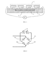
- the light emitting device comprises an LED chip 1 and an AC driving circuit chip 5, wherein the AC driving circuit chip 5 comprises a substrate 2 and a rectifying circuit 3 integrated on the substrate, the LED chip 1 is flip-chip bonded on the AC driving circuit chip 5 and electrically connected to the rectifying circuit 3.
- the LED chip 1 On each of both ends of the substrate 2 of the AC driving circuit chip 5 is provided a power source connecting terminal for externally connecting an AC power source.
- the LED chip 1 has a plurality of mutually independent light emitting regions 101 which are connected in series or in parallel.
- the rectifying circuit 3 comprises a first diode 301, a second diode 302, a third diode 303 and a fourth diode 304.
- the first diode 301 and the fourth diode 304 are connected in series to form a first branch
- the second diode 302 and the third diode 303 are connected in series to form a second branch
- the first branch and the second branch are connected in parallel to form an AC/DC bridge rectifier.
- the first branch and the second branch after being connected in parallel, are connected in series with each light emitting region 101 in the LED chip 1.
- a connection point between the first diode 301 and the fourth diode 304, and a connection point between the second diode 302 and the third diode 303 are respectively electrically connected to the power source connecting terminals on the substrate 2 of the AC driving circuit chip 5, thereby being externally connected to the AC power source.
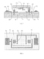
- Fig.3 is a cross-sectional view of the first embodiment of the light emitting device according to the present invention
- Fig.4 is a top view of a surface of a substrate of the light emitting device shown in Fig.3 .
- the LED chip 1 is divided into two light emitting regions 101a and 101b, each light emitting region 101 has a P electrode and an N electrode, the N electrode of the light emitting region 101a is adjacent to the P electrode of the light emitting region 101b, and they are electrically connected to each other through a second metal wire layer 102.
- the rectifying circuit 3 is integrated on the substrate 2 to form the AC driving circuit chip 5. Specifically speaking, on the substrate 2 are formed the first diode 301, the second diode 302, the third diode 303 and the fourth diode 304. An upper surface of the substrate 2 is covered with an insulating layer 202, a contact hole e is provided at the insulating layer 202 corresponding to the P and N electrodes of the diode, a first metal wire layer 203 is provided on an upper surface of the insulating layer 202 and respectively electrically connected to the P and N electrodes of each diode through the contact hole e.
- the first diode 301 and the second diode 302 are P-N type diodes, wherein the N electrodes thereof are electrically connected through the first metal wire layer 203 to form an N-type connecting terminal;
- the third diode 303 and the fourth diode 304 are N-P type diodes, wherein the P electrodes thereof are electrically connected through the first metal wire layer 203 to form a P-type connecting terminal.
- the P electrode of the first diode 301 and the N electrode of the fourth diode 304 are connected to a power source connecting terminal via the first metal wire layer 203, and the P electrode of the second diode and the N electrode of the third diode are connected to another power source connecting terminal via the first metal wire layer 203.
- a UBM layer On upper surfaces of the P-type connecting terminal and the N-type connecting terminal are respectively provided a UBM layer, and on upper surfaces of the two power source connecting terminals are respectively provided an external bond pad 206. On an upper surface of the UBM layer 204 is provided a metal bump 205.
- the LED chip 1 is flip-chip bonded on the AC driving circuit chip 5 , the P electrode of the first light emitting region of the LED chip 1 is connected to the metal bump 205 which corresponds to the N-type connecting terminal of the substrate 2, and the N electrode of the second light emitting region is connected to the metal bump 205 which corresponds to the P-type connecting terminal of the substrate 2.
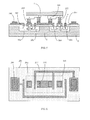
- Fig.5 is a cross-sectional view of a second embodiment of the light emitting device according to the present invention
- Fig.6 is a top view of a surface of a substrate of the light emitting device shown in Fig.5 .
- the light emitting device according to Embodiment 2 is structurally substantially the same as that in Embodiment 1.
- the same rectifying circuit 3 is integrated on the substrate 2.
- the P electrode and N electrode of the light emitting region 101 on the light emitting diode chip 1 are both connected to the metal bump 205 of the substrate 2 by flip-chip, i.e., adjacent N electrode and P electrode in two adjacent light-emitting regions 101 are respectively connected to the metal bump 205 at a corresponding position of the upper surface of the substrate 2, and achieve in-series connection through the first metal wire layer 203 on the substrate 2.
- a method of manufacturing the light emitting device according to Embodiment 2 specifically comprises the following steps:
- Fig.7 is a schematic view of a circuit of the light emitting device using AC according to a third embodiment of the present invention.
- the circuit of the light emitting device comprises a plurality of LED chips 103, a rectifying circuit 3 and a filter circuit 4.
- the plurality of LED chips 103 are mutually connected in series.
- the filter circuit 4 comprises a resistor 401 and a capacitor 402 connected in parallel.
- the rectifying circuit 3 is a bridge rectifying circuit which is structured the same as the rectifying circuit of Embodiment 1.
- the filter circuit 4 is connected in series at a power source input end of the rectifying circuit 3.
- the plurality of LED chips 103 connected in series are connected in series at an output end of the rectifying circuit 103.
- Fig.8 is a cross-sectional view of the light emitting device according to the third embodiment of the present invention
- Fig.9 is a top view on surface of the substrate of the light emitting device shown in Fig.8 .
- the LED chip 103 has a light emitting region which has a P electrode and an N electrode.
- the rectifying circuit 3 and the filter circuit 4 are together integrated on the substrate 2 to form the AC driving circuit chip 6, the filter circuit 4 is disposed between the rectifying circuit 3 and a power source connecting terminal.
- the integrated circuit wiring of the rectifying circuit 3 is identical with that in Embodiment 2.
- the resistor 401 of the filter circuit 4 is disposed on the upper surface of the insulating layer 202 on the upper surface of the substrate. It increases the length because the resistor 401 can be provided in a winding shape according to a present resitivity, and thereby it increases the resisitivity of the resistor 401.
- the resistor 401 is made of polycrystalline silicon, and is structured in three layers: a conductive layer and an insulating layer and a conductive layer (not shown in Figs).
- the conductive layer on the bottom is disposed on the insulating layer 202 and electrically connected to the first metal wire layer 203, and the conductive layer on the top of the capacitor 402 is connected through a third metal wire layer 207 to the first metal wire layer 203 connected to the power source connecting terminal.
- the plurality of LED chips 103 are flip-chip bonded on the substrate 2 of the AC driving circuit chip 6, the P electrode and the N electrode of each of the LED chips 103 are respectively connected to the metal bump 205 at the corresponding position on the substrate 2, in order to form a circuit loop of the light emitting device shown in Fig.7 .
- a manufacturing method about the light emitting device according to Embodiment 3 specifically comprises the following steps in detail:
- the manufacturing steps of the filter circuit 4 can be finished between S4 and S5.
- the UBM layer 204, the external bond pad 206 and the metal bump 205 are formed after the rectifying circuit 3 and the filter circuit 4 are integrated on the substrate 2.
- the rectifying circuit of the present invention is not limited to the bridge rectifying circuit formed by the diodes connected in series and parallel, and it can be a rectifying circuit with other structures.
- the AC driving circuit chip of the present invention can further be integrated with circuits or elements in other forms so that the AC/DC conversion function becomes more stable.
- the light emitting regions in the LED chips or one LED chip of the present invention can not only be connected in series, but also connected in parallel or connected simultaneously in series and parallel.
- the rectifying circuit is integrated on the substrate to form the AC driving circuit chip and then the LED chip is directly flip-chip bonded on the AC driving circuit chip so that AC power source can be directly introduced in the light emitting device without needing any external integrated circuit device or electronic parts, thereby it can save the assembling space and improving flexibility in using.
- the LED chip is flip-chip bonded on the substrate, and does not require connection modes such as routing or circuit board connection, thereby improving its reliability.
Landscapes
- Led Device Packages (AREA)
- Led Devices (AREA)
Applications Claiming Priority (1)
| Application Number | Priority Date | Filing Date | Title |
|---|---|---|---|
| CN2010101900521A CN101886759B (zh) | 2010-05-24 | 2010-05-24 | 一种使用交流电的发光器件及其制造方法 |
Publications (2)
| Publication Number | Publication Date |
|---|---|
| EP2390918A2 true EP2390918A2 (de) | 2011-11-30 |
| EP2390918A3 EP2390918A3 (de) | 2013-04-17 |
Family
ID=43072779
Family Applications (1)
| Application Number | Title | Priority Date | Filing Date |
|---|---|---|---|
| EP10190698.0A Withdrawn EP2390918A3 (de) | 2010-05-24 | 2010-11-10 | Lichtemittierende Vorrichtung mit Wechselstrom und Herstellungsverfahren dafür |
Country Status (5)
| Country | Link |
|---|---|
| US (1) | US20110285284A1 (de) |
| EP (1) | EP2390918A3 (de) |
| JP (1) | JP5636251B2 (de) |
| CN (1) | CN101886759B (de) |
| WO (1) | WO2011147063A1 (de) |
Cited By (1)
| Publication number | Priority date | Publication date | Assignee | Title |
|---|---|---|---|---|
| TWI577058B (zh) * | 2014-11-14 | 2017-04-01 | Bidirectional light emitting diodes and their lighting devices |
Families Citing this family (17)
| Publication number | Priority date | Publication date | Assignee | Title |
|---|---|---|---|---|
| US8222726B2 (en) * | 2010-03-29 | 2012-07-17 | Advanced Semiconductor Engineering, Inc. | Semiconductor device package having a jumper chip and method of fabricating the same |
| DE102012111247A1 (de) | 2012-11-21 | 2014-05-22 | Osram Opto Semiconductors Gmbh | Optoelektronisches Halbleiterbauteil |
| US20140209961A1 (en) * | 2013-01-30 | 2014-07-31 | Luxo-Led Co., Limited | Alternating current light emitting diode flip-chip |
| CN103337582B (zh) * | 2013-06-19 | 2015-04-22 | 深圳市源磊科技有限公司 | Led光源及其制造方法 |
| WO2015052616A1 (en) * | 2013-10-09 | 2015-04-16 | Koninklijke Philips N.V. | Monolithic led arrays for uniform and high-brightness light sources |
| CN104752594B (zh) * | 2013-12-25 | 2017-11-10 | 宝钢金属有限公司 | 一种用于ac‑led芯片结构倒装焊金属层的制作方法 |
| CN104752578A (zh) * | 2013-12-25 | 2015-07-01 | 宝钢金属有限公司 | 一种用于ac-led芯片结构倒装焊金属层结构 |
| DE102014105734A1 (de) * | 2014-04-23 | 2015-10-29 | Osram Opto Semiconductors Gmbh | Optoelektronisches Halbleiterbauteil und Verfahren zur Herstellung eines optoelektronischen Halbleiterbauteils |
| CN104994634A (zh) * | 2015-06-29 | 2015-10-21 | 宝钢金属有限公司 | 一种ac-led集成芯片 |
| US10079264B2 (en) * | 2015-12-21 | 2018-09-18 | Hong Kong Beida Jade Bird Display Limited | Semiconductor devices with integrated thin-film transistor circuitry |
| BR112018012830A2 (pt) * | 2015-12-23 | 2018-12-04 | Koninklijke Philips Nv | estrutura marinha |
| US10332949B2 (en) | 2016-07-06 | 2019-06-25 | Seoul Semiconductor Co., Ltd. | Display apparatus |
| JP7071618B2 (ja) * | 2016-11-30 | 2022-05-19 | 日亜化学工業株式会社 | 発光装置及び基板 |
| CN113110439B (zh) * | 2021-04-08 | 2022-10-28 | 江苏大学 | 一种实时可抗风浪无人船的航线控制方法及其水质监测系统 |
| FR3123733B1 (fr) * | 2021-06-08 | 2024-06-21 | St Microelectronics Grenoble 2 | Boîtier optique de circuit integre |
| CN217955870U (zh) * | 2021-06-08 | 2022-12-02 | 意法半导体(格勒诺布尔2)公司 | 集成电路封装 |
| CN114811459A (zh) * | 2022-04-20 | 2022-07-29 | 龙岩德煜照明有限公司 | 一种led发光模块及应用的led灯丝、紧凑型led灯泡 |
Citations (4)
| Publication number | Priority date | Publication date | Assignee | Title |
|---|---|---|---|---|
| US7148515B1 (en) * | 2006-01-07 | 2006-12-12 | Tyntek Corp. | Light emitting device having integrated rectifier circuit in substrate |
| CN201043720Y (zh) | 2007-06-19 | 2008-04-02 | 天津医科大学总医院 | 交流led灯 |
| CN101586791A (zh) | 2009-03-13 | 2009-11-25 | 厦门市光电工程技术研究中心 | 一种简约节能半导体灯 |
| US20100060181A1 (en) | 2008-09-05 | 2010-03-11 | Seoul Semiconductor Co., Ltd. | Ac led dimmer and dimming method thereby |
Family Cites Families (20)
| Publication number | Priority date | Publication date | Assignee | Title |
|---|---|---|---|---|
| US6121104A (en) * | 1997-12-12 | 2000-09-19 | Texas Instruments Incorporated | Charge cancellation technique for integrated circuit resistors |
| CN2545706Y (zh) * | 2002-03-29 | 2003-04-16 | 苏州固锝电子有限公司 | 片式微型桥堆 |
| US20040206970A1 (en) * | 2003-04-16 | 2004-10-21 | Martin Paul S. | Alternating current light emitting device |
| EP1656700A1 (de) * | 2003-08-12 | 2006-05-17 | Philips Intellectual Property & Standards GmbH | Schaltungsanordnung zur wechselstrom-ansteuerung organischer dioden |
| US6898068B2 (en) * | 2003-09-24 | 2005-05-24 | Texas Instruments Incorporated | Dual mask capacitor for integrated circuits |
| KR100961483B1 (ko) * | 2004-06-30 | 2010-06-08 | 서울옵토디바이스주식회사 | 다수의 셀이 결합된 발광 소자 및 이의 제조 방법 및 이를이용한 발광 장치 |
| US7221044B2 (en) * | 2005-01-21 | 2007-05-22 | Ac Led Lighting, L.L.C. | Heterogeneous integrated high voltage DC/AC light emitter |
| US8076680B2 (en) * | 2005-03-11 | 2011-12-13 | Seoul Semiconductor Co., Ltd. | LED package having an array of light emitting cells coupled in series |
| EP2536255B1 (de) * | 2005-06-28 | 2014-03-19 | Seoul Opto Device Co., Ltd. | Licht emittierende Vorrichtung zum Wechselstrombetrieb |
| KR100634307B1 (ko) * | 2005-08-10 | 2006-10-16 | 서울옵토디바이스주식회사 | 발광 소자 및 이의 제조 방법 |
| JP2007188942A (ja) * | 2006-01-11 | 2007-07-26 | Tyntek Corp | 整流回路を副キャリアに結合した発光ダイオードの発光装置及びその製造方法 |
| CN101154656B (zh) * | 2006-09-30 | 2010-05-12 | 香港微晶先进封装技术有限公司 | 多芯片发光二极管模组结构及其制造方法 |
| US7863825B2 (en) * | 2007-01-30 | 2011-01-04 | Addtek Corp. | LED driver circuit for providing desired luminance with constant current |
| JP2010511971A (ja) * | 2007-09-14 | 2010-04-15 | エスエムクリエーション リミテッド | 安定器を有する蛍光灯用のled照明灯 |
| JP2009105355A (ja) * | 2007-10-23 | 2009-05-14 | Daiichi-Tsusho Co Ltd | Led照明器具 |
| US8062916B2 (en) * | 2008-11-06 | 2011-11-22 | Koninklijke Philips Electronics N.V. | Series connected flip chip LEDs with growth substrate removed |
| CN201335281Y (zh) * | 2009-01-06 | 2009-10-28 | 常州机电职业技术学院 | 节能照明装置 |
| CN201412704Y (zh) * | 2009-03-10 | 2010-02-24 | 广州南科集成电子有限公司 | 一种集成led芯片的光源 |
| CN101908534B (zh) * | 2009-06-08 | 2012-06-13 | 晶元光电股份有限公司 | 发光装置 |
| CN201680214U (zh) * | 2010-05-24 | 2010-12-22 | 晶科电子(广州)有限公司 | 一种使用交流电的发光器件 |
-
2010
- 2010-05-24 CN CN2010101900521A patent/CN101886759B/zh active Active
- 2010-10-08 WO PCT/CN2010/001571 patent/WO2011147063A1/zh not_active Ceased
- 2010-10-13 JP JP2010230330A patent/JP5636251B2/ja active Active
- 2010-10-25 US US12/911,372 patent/US20110285284A1/en not_active Abandoned
- 2010-11-10 EP EP10190698.0A patent/EP2390918A3/de not_active Withdrawn
Patent Citations (4)
| Publication number | Priority date | Publication date | Assignee | Title |
|---|---|---|---|---|
| US7148515B1 (en) * | 2006-01-07 | 2006-12-12 | Tyntek Corp. | Light emitting device having integrated rectifier circuit in substrate |
| CN201043720Y (zh) | 2007-06-19 | 2008-04-02 | 天津医科大学总医院 | 交流led灯 |
| US20100060181A1 (en) | 2008-09-05 | 2010-03-11 | Seoul Semiconductor Co., Ltd. | Ac led dimmer and dimming method thereby |
| CN101586791A (zh) | 2009-03-13 | 2009-11-25 | 厦门市光电工程技术研究中心 | 一种简约节能半导体灯 |
Cited By (1)
| Publication number | Priority date | Publication date | Assignee | Title |
|---|---|---|---|---|
| TWI577058B (zh) * | 2014-11-14 | 2017-04-01 | Bidirectional light emitting diodes and their lighting devices |
Also Published As
| Publication number | Publication date |
|---|---|
| WO2011147063A1 (zh) | 2011-12-01 |
| JP5636251B2 (ja) | 2014-12-03 |
| JP2011249755A (ja) | 2011-12-08 |
| EP2390918A3 (de) | 2013-04-17 |
| US20110285284A1 (en) | 2011-11-24 |
| CN101886759A (zh) | 2010-11-17 |
| CN101886759B (zh) | 2012-07-25 |
Similar Documents
| Publication | Publication Date | Title |
|---|---|---|
| EP2390918A2 (de) | Lichtemittierende Vorrichtung mit Wechselstrom und Herstellungsverfahren dafür | |
| US7148515B1 (en) | Light emitting device having integrated rectifier circuit in substrate | |
| CN100508186C (zh) | 贴片式发光二极管及制造方法 | |
| TW201438188A (zh) | 堆疊式發光二極體陣列結構 | |
| KR20060001800A (ko) | 다수의 셀이 결합된 발광 소자 및 이의 제조 방법 및 이를이용한 발광 장치 | |
| CN103426989A (zh) | 半导体发光器件及其制造方法、发光模块和照明设备 | |
| JP5858854B2 (ja) | Ledモジュール | |
| US9743521B2 (en) | Light-source module and light-emitting device | |
| US8519428B2 (en) | Vertical stacked light emitting structure | |
| JP2018022930A (ja) | 発光デバイス及びその製造方法 | |
| JP2008091459A (ja) | Led照明装置及びその製造方法 | |
| JP5946311B2 (ja) | Ledモジュール | |
| CN101982883A (zh) | 一种由倒装发光单元阵列组成的发光器件及其制造方法 | |
| CN102130107B (zh) | 阶梯阵列式高压发光管及其制备方法 | |
| US12359779B1 (en) | LED filament and LED light bulb | |
| CN201680214U (zh) | 一种使用交流电的发光器件 | |
| KR101216938B1 (ko) | 다수의 셀이 결합된 발광 소자 및 이의 제조 방법 및 이를이용한 발광 장치 | |
| CN201069771Y (zh) | 贴片式发光二极管 | |
| US20120267645A1 (en) | Light emitting diode module package structure | |
| KR101121714B1 (ko) | 발광 장치 | |
| KR101229835B1 (ko) | 다수의 셀이 결합된 발광 소자 및 이의 제조 방법 및 이를 이용한 발광 디바이스 | |
| CN201804867U (zh) | 一种由倒装发光单元阵列组成的发光器件 | |
| KR101203139B1 (ko) | 다수의 셀이 결합된 발광 소자 | |
| CN218939723U (zh) | 高亮度cob封装结构以及led灯 | |
| CN103594587A (zh) | 一种发光二极管打线电极的制造方法 |
Legal Events
| Date | Code | Title | Description |
|---|---|---|---|
| AK | Designated contracting states |
Kind code of ref document: A2 Designated state(s): AL AT BE BG CH CY CZ DE DK EE ES FI FR GB GR HR HU IE IS IT LI LT LU LV MC MK MT NL NO PL PT RO RS SE SI SK SM TR |
|
| AX | Request for extension of the european patent |
Extension state: BA ME |
|
| PUAI | Public reference made under article 153(3) epc to a published international application that has entered the european phase |
Free format text: ORIGINAL CODE: 0009012 |
|
| PUAL | Search report despatched |
Free format text: ORIGINAL CODE: 0009013 |
|
| AK | Designated contracting states |
Kind code of ref document: A3 Designated state(s): AL AT BE BG CH CY CZ DE DK EE ES FI FR GB GR HR HU IE IS IT LI LT LU LV MC MK MT NL NO PL PT RO RS SE SI SK SM TR |
|
| AX | Request for extension of the european patent |
Extension state: BA ME |
|
| RIC1 | Information provided on ipc code assigned before grant |
Ipc: H01L 33/00 20100101ALI20130314BHEP Ipc: H01L 25/16 20060101AFI20130314BHEP Ipc: H05B 33/08 20060101ALN20130314BHEP |
|
| 17P | Request for examination filed |
Effective date: 20130926 |
|
| RBV | Designated contracting states (corrected) |
Designated state(s): AL AT BE BG CH CY CZ DE DK EE ES FI FR GB GR HR HU IE IS IT LI LT LU LV MC MK MT NL NO PL PT RO RS SE SI SK SM TR |
|
| 17Q | First examination report despatched |
Effective date: 20131105 |
|
| STAA | Information on the status of an ep patent application or granted ep patent |
Free format text: STATUS: THE APPLICATION IS DEEMED TO BE WITHDRAWN |
|
| 18D | Application deemed to be withdrawn |
Effective date: 20160802 |