EP2387155B1 - Verfahren zur Übertragung eines binären Signals über eine Übertragerstrecke - Google Patents
Verfahren zur Übertragung eines binären Signals über eine Übertragerstrecke Download PDFInfo
- Publication number
- EP2387155B1 EP2387155B1 EP11162075.3A EP11162075A EP2387155B1 EP 2387155 B1 EP2387155 B1 EP 2387155B1 EP 11162075 A EP11162075 A EP 11162075A EP 2387155 B1 EP2387155 B1 EP 2387155B1
- Authority
- EP
- European Patent Office
- Prior art keywords
- signal
- pulse
- value
- output
- transformer
- Prior art date
- Legal status (The legal status is an assumption and is not a legal conclusion. Google has not performed a legal analysis and makes no representation as to the accuracy of the status listed.)
- Active
Links
Images


Classifications
-
- H—ELECTRICITY
- H03—ELECTRONIC CIRCUITRY
- H03K—PULSE TECHNIQUE
- H03K17/00—Electronic switching or gating, i.e. not by contact-making and –breaking
- H03K17/18—Modifications for indicating state of switch
-
- H—ELECTRICITY
- H03—ELECTRONIC CIRCUITRY
- H03B—GENERATION OF OSCILLATIONS, DIRECTLY OR BY FREQUENCY-CHANGING, BY CIRCUITS EMPLOYING ACTIVE ELEMENTS WHICH OPERATE IN A NON-SWITCHING MANNER; GENERATION OF NOISE BY SUCH CIRCUITS
- H03B1/00—Details
-
- H—ELECTRICITY
- H03—ELECTRONIC CIRCUITRY
- H03K—PULSE TECHNIQUE
- H03K17/00—Electronic switching or gating, i.e. not by contact-making and –breaking
-
- H—ELECTRICITY
- H03—ELECTRONIC CIRCUITRY
- H03K—PULSE TECHNIQUE
- H03K17/00—Electronic switching or gating, i.e. not by contact-making and –breaking
- H03K17/51—Electronic switching or gating, i.e. not by contact-making and –breaking characterised by the components used
- H03K17/56—Electronic switching or gating, i.e. not by contact-making and –breaking characterised by the components used by the use, as active elements, of semiconductor devices
- H03K17/60—Electronic switching or gating, i.e. not by contact-making and –breaking characterised by the components used by the use, as active elements, of semiconductor devices the devices being bipolar transistors
- H03K17/605—Electronic switching or gating, i.e. not by contact-making and –breaking characterised by the components used by the use, as active elements, of semiconductor devices the devices being bipolar transistors with galvanic isolation between the control circuit and the output circuit
- H03K17/61—Electronic switching or gating, i.e. not by contact-making and –breaking characterised by the components used by the use, as active elements, of semiconductor devices the devices being bipolar transistors with galvanic isolation between the control circuit and the output circuit using transformer coupling
-
- H—ELECTRICITY
- H03—ELECTRONIC CIRCUITRY
- H03K—PULSE TECHNIQUE
- H03K17/00—Electronic switching or gating, i.e. not by contact-making and –breaking
- H03K17/51—Electronic switching or gating, i.e. not by contact-making and –breaking characterised by the components used
- H03K17/56—Electronic switching or gating, i.e. not by contact-making and –breaking characterised by the components used by the use, as active elements, of semiconductor devices
- H03K17/687—Electronic switching or gating, i.e. not by contact-making and –breaking characterised by the components used by the use, as active elements, of semiconductor devices the devices being field-effect transistors
- H03K17/689—Electronic switching or gating, i.e. not by contact-making and –breaking characterised by the components used by the use, as active elements, of semiconductor devices the devices being field-effect transistors with galvanic isolation between the control circuit and the output circuit
- H03K17/691—Electronic switching or gating, i.e. not by contact-making and –breaking characterised by the components used by the use, as active elements, of semiconductor devices the devices being field-effect transistors with galvanic isolation between the control circuit and the output circuit using transformer coupling
-
- H—ELECTRICITY
- H03—ELECTRONIC CIRCUITRY
- H03K—PULSE TECHNIQUE
- H03K3/00—Circuits for generating electric pulses; Monostable, bistable or multistable circuits
-
- H—ELECTRICITY
- H04—ELECTRIC COMMUNICATION TECHNIQUE
- H04L—TRANSMISSION OF DIGITAL INFORMATION, e.g. TELEGRAPHIC COMMUNICATION
- H04L25/00—Baseband systems
- H04L25/02—Details ; arrangements for supplying electrical power along data transmission lines
Definitions
- the invention relates to a method for the repetitive transmission of a signal representing a binary value via a transmission path of a driver of a power semiconductor.
- a so-called driver circuit or a short driver is necessary. For example, generates the driver from a signal supplied to the driver at the input low power logical switching signal to be applied to the output of the driver to the power semiconductor signal with significantly increased power, which is necessary for example for actually switching an IGBT.
- the driver accepts galvanic isolation between its input and output, e.g. the switching signal or operating at ground potential control logic and the power semiconductor, which operates at high voltage potential.
- a binary signal ie a signal representing a binary value
- the transformer causes the potential separation in the signal to be transmitted.
- An appropriate binary signal is eg a start-up or switch-off signal for the transformer.
- a signal in the form of a switching signal only knows the two signal values "on” and "off".
- the transformer or its magnetization passes into a positive or negative saturation by repetitively applying the respective same positive or negative voltage pulses.
- the time between two equal successive repetitive pulses as the recovery time for the transformer, so that it can at least partially demagnetize again. So it is a minimum time or minimum dead time between two identical repetitive pulses to comply.
- a driver for driving a semiconductor switch wherein a modulated drive signal for driving the semiconductor switch is transmitted via a transformer from a primary side of the driver to a secondary side of the driver and is demodulated again on the secondary side of the driver.
- a switching control circuit for driving a transistor is known in which the transistor via a pulse transformer of the switching control circuit by means of pulses which are transmitted via the pulse transformer to a threshold circuit of the switching control circuit is turned on or off.
- the object of the invention is to specify an improved method for the repetitive transmission of a signal representing a binary value via a transmission path of a driver of a power semiconductor.
- the object is achieved by a method according to claim 1.
- the input of the transformer for the first of the binary values of the signal is a first pulse packet as a result of a positive and negative pulse - starting from a center signal layer - supplied.
- a second pulse packet is supplied to the transmitter for the second value of the binary signal as a result of a negative and positive pulse.
- a pulse can be eg a current or voltage pulse.
- the transmitter is thus, for example, starting from a center voltage, a consequence of a positive and negative voltage pulse or voltage or a negative-positive sequence. Also, for example, starting from a zero current, a short positive, followed by a negative current pulse or vice versa, are supplied.
- the respective same packets are fed repetitively to the transmitter.
- the polarity of an output variable is then monitored or evaluated. be an output voltage or an output current of the transformer.
- the evaluation does not now take place solely from one of the two pulses, but from their entirety or the entire signal course within the pulse train. Only from the consequence of the polarity or the polarity change of the output variable within a transmitted packet thus the first or second value of the binary signal is detected. The only condition for this is that the packet boundaries must be recognizable at the output of the transformer, e.g. by observing certain set timing limits.
- each pulse packet in each case both a positive and a negative pulse it can be prevented that the transmitter goes into saturation.
- the positive and negative pulses with respect to their containing energy adapted to each other, for example, so that their magnetization effect in the transformer at least approximately compensated.
- the transformer through the particular impulse packet is not saturated, in particular not the above-mentioned compulsory pauses or dead times between two repetitive pulse packets of the same binary value must be complied with.
- the pulse packets can follow one another at almost any desired speed, in particular at any desired interval, while maintaining the above-mentioned conditions for detecting the packet boundaries.
- the Studentstragerrange in a driver can be both from the primary to the secondary side as well as in the opposite direction.
- the prerequisite for the method according to the invention is merely that the signal receiver, i. the output side connected to the transformer evaluation can evaluate both positive and negative output signals of the transformer.
- the first signal may e.g. be a switching signal to be transmitted from the primary to the secondary side or an error signal to be transmitted in the opposite direction.
- the respective amplitudes of the pulses within the pulse packets are at least approximately equal.
- a pulse packet consists of e.g. two equally high pulses of opposite sign. If its duration is the same, the energy content of the pulses will be the same again as above.
- the binary signal is a first signal and at the input of the transformer, the time interval between two repetitive successive pulse packets of the same value of the first signal is varied in response to a second signal to be transmitted. At the output then the time interval determined from the detected, imaged in the output pulse packets and reconstructs the second signal from the output determined time interval.
- a second signal can be superimposed.
- the second signal may be e.g. be a binary signal, which knows only two values and thus two time intervals between successive pulse packets.
- several values or a continuous signal as a second signal are conceivable, i. There are several different or continuously varying time intervals between pulse packets.
- a change in the value of the first signal can usually take place at any time, so that the time interval between a last pulse packet of the one binary value of the first signal and the first pulse packet of the other binary value is not recognized as a valid second signal may be.
- a value change in the first signal at this point usually destroys the value of the second signal.
- the second signal may e.g. be the value of a DC link voltage or a soft-off switching signal.
- the pulse duration of the pulse is varied in dependence on a signal to be transmitted by a third party.
- the pulse duration of the pulse is then determined and the third signal is reconstructed from the pulse duration.
- additional information in the form of the third signal can be transmitted, which, like the second signal, can be binary, multi-valued or continuous.
- the change of the first binary signal is only allowed or transmitted outside the duration of pulse packets.
- First and third signal would not disturb each other. In general, however, the precedence of the first signal will be desirable if, for example, this is a switching signal for a power semiconductor switch, but the second and third signals represent, for example, less critical data to be transmitted.
- the third signal may e.g. represent the value of a measured temperature.
- All three above-mentioned possibilities for signal transmission from the first to the third signal can thus be used independently of one another or together in corresponding combinations, both from the primary to the secondary side and vice versa.
- the transmission of the signals always takes place in parallel in the same direction.
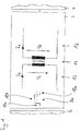
- Fig. 1 shows a driver 2 for a power semiconductor 4, which is supplied by a logic circuit 6 with a signal 8 as a switching signal for the switching states "on” or “off” of the power semiconductor 4.
- the signal 8 is thus a binary signal or has only two values 10a corresponding to "off” and 10b corresponding to "on”.
- the signal 8 is applied to an input 12 of a transformer 14, which causes the galvanically separating transmission of the signal 8 to the output 16.
- the transformer 14 has at its input 12 as input variables an input current I E and an input voltage UE and at its output as output variables an output current I A and an output voltage U A.
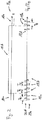
- Fig. 2 again shows the signal 8 in an enlarged view, plotted against the time t.
- the transmitter 14 is repretetively fed pulse packets 18a, b respectively.
- pulse packets 18a are selected, for the value 10b pulse packets 18b.
- the pulse packets 18a each consist of a sequence of a negative pulse 20a followed by a positive pulse 20b, whereas the positive pulse packets 18b consist of a positive pulse 20b followed by a negative pulse 20a.
- the respective packets 18a or 18b are each sent repetitively, ie at a time interval T R.
- the respective pulse 20a or 20b corresponds to Fig. 1 a respective positive or negative value of the current I E or alternatively a positive or negative value of the voltage U E.
- corresponding signal curves for the output voltage U A and the output current I A are set .
- the respective sequence of the polarity of the pulse packets 18a or 18b also results in different polarity sequences for the output current I A or the output voltage U A.
- Figure 3 shows, for example, how a sequence 22a of an initially positive and later negative pulse 24a, b results for the pulse packet 18a.
- a pulse packet 18b is applied to the input 12
- a sequence 22b of a negative pulse 24b and of a positive pulse 24a results.
- the corresponding pulse sequence at the input 12 and thus the corresponding value 10a, b of the signal 8 is closed on the output 16 side.
- Detection takes place in each case on the basis of the totality of the sequences 22a, b, that is also on the basis of the entire pulse packet 18a, b, and not only on the part (pulses 24a or 24b) of the sequences 22a, b which are to be assigned to a single pulse 20a or 20b ,
- the evaluation can be based on the slope profile (positive or negative zero crossing) between the respective pulses 24a, b, ie in each case approximately centrally in the sequence 22a, b done.
- Figure 3 also shows an embodiment in which the amplitudes A 0 and -A 0 of the two pulses 20a, b of the pulse packets 18a, b are equal in magnitude (Ao) but opposite in sign.
- This also offers the possibility to evaluate the entire two pulses 24a, b, also in terms of their amplitudes, in their entirety. Both amplitudes should then again be about the same size and have opposite sign. Also, an evaluation of the entire pulse sequence 18a, b and not only their partial pulses 20a, b with respect to the detection of the binary values to be transmitted (first or second value).
- the respective time intervals T R are always the same size, the repetitive repetition of the same pulse packets 18 a, b thus takes place with a fixed repetition frequency.
- a second signal 8b is transmitted via the transmitter 14 parallel to the first signal 8a by the use of different or signal-dependent varying time intervals T R.
- Fig. 4 shows that in addition to the signal 8a still the signal 8b is transmitted.
- This also has only two values 26a, b in the example.
- the values 26a, b are converted into different distances T R.
- the time intervals T R1 in this case correspond to the value 26a, the time intervals T R2 to the value 26b.
- the corresponding time intervals T R1,2 again become as indicated Fig. 3 at the Output 16 is also evaluated or recognized as time intervals between two sequences 22a, b and thereby the values 26a, b reconstructed.
- Fig. 5 shows an alternative embodiment for representing a third signal 8c and its transmission via the transmitter 14.
- the signal 8a is coded in a conventional manner, the values 28a, b of the signal 8c, however, by different pulse durations T P1,2 of the individual pulses 18a, b coded.
- the evaluation at the output 16 takes place again according to the differentiation of the pulse durations of the pulses 24a, b or of the sequences 22a, b correspondingly Fig. 3 ,
Landscapes
- Engineering & Computer Science (AREA)
- Power Engineering (AREA)
- Computer Networks & Wireless Communication (AREA)
- Signal Processing (AREA)
- Dc Digital Transmission (AREA)
Description
- Verfahren zur Übertragung eines binären Signals über eine Übertragerstrecke.
- Die Erfindung betrifft ein Verfahren zur repetitiven Übertragung eines einen binären Wert repräsentierenden Signals über eine Übertragerstrecke eines Treibers eines Leistungshalbleiters.
- Zur Ansteuerung eines Leistungshalbleiters, z.B. eines Leistungshalbleiterschalters in Form eines IGBT (insulated-gate bipolar transistor), ist eine sogenannten Treiberschaltung oder kurz ein Treiber notwendig. Z.B. erzeugt der Treiber aus einem dem Treiber am Eingang zugeführten logischen Schaltsignal schwacher Leistung ein am Ausgang des Treibers an den Leistungshalbleiter anzulegendes Signal mit deutlich erhöhter Leistung, welche beispielsweise zum tatsächlichen Schalten eines IGBT notwendig ist. Außerdem übernimmt der Treiber eine galvanische bzw. Potentialtrennung zwischen seinem Eingang und Ausgang, z.B. dem Schaltsignal bzw. einer auf Erdpotential arbeitenden Ansteuerlogik und dem Leistungshalbleiter, welcher auf Hochspannungspotential arbeitet.
- In der Regel wird innerhalb dieses Treibers daher ein binäres Signal, d.h. ein Signal, das einen binären Wert repräsentiert, über eine Übertragerstrecke des Treibers übertragen. Der Übertrager bewirkt die Potentialtrennung im zu übertragenenden Signal. Ein entsprechendes binäres Signal ist z.B. ein Einschalt- bzw. Ausschaltsignal für den Übertrager. Ein Signal in Form eines Schaltsignals kennt z.B. nur die beiden Signalwerte "Ein" und "Aus". Um eine hohe Schaltsicherheit zu erzielen, ist es üblich, entsprechende Signale bzw. Signalwerte repetitiv zu übertragen. Bekannt ist es z.B., beim Anlegen eines Einschaltsignals dem Übertrager als ersten binären Wert - z.B. ausgehend von einem Mittenpotential - repetitiv positive Spannungsimpulse zuzuführen. Diese Impulse werden dem Übertrager so lange zugeführt, bis ein Ausschalten des Leistungshalbleiters gewünscht ist. Ausgehend vom Mittenpotenzial werden daraufhin dem Übertrager repetitiv negative Spannungspulse zugeführt.
- Sowohl während Anliegen des Einschalt- als auch des Ausschaltsignals gelangt der Übertrager bzw. dessen Magnetisierung durch repetitives Anlegen der jeweiligen gleichen positiven oder negativen Spannungspulse in eine positive oder negative Sättigung. Um eine Sättigung des Übertragers zu vermeiden, ist es bekannt, die Zeit zwischen zwei gleichen aufeinanderfolgenden repetitiv angelegten Impulsen als Erholungszeit für den Übertrager zu nutzen, damit sich dieser zumindest teilweise wieder entmagnetisieren kann. Es ist also eine Mindestzeit bzw. minimale Totzeit zwischen zwei gleichen repetitiven Pulsen einzuhalten.
- Aus der
US 2009/0147544 A1 ist ein Treiber zur Ansteuerung eines Halbleiterschalters bekannt, wobei ein moduliertes Ansteuersignal zur Ansteuerung des Halbleiterschalters über einen Transformator von einer Primärseite des Treibers auf eine Sekundärseite des Treibers übertragen wird und auf der Sekundärseite des Treibers wieder demoduliert wird. - Aus der
US 2004/0080885 A1 ist eine Antriebssteuerung für einen elektrischen Antrieb mit einem Leistungsteil bekannt, das auf einem hohen elektrischen Potential liegt, wobei die Antriebssteuerung eine Ansteuerelektronik, die dem Leistungsteil Ansteuersignale liefert und von diesem Phasenstromistwerte erhält und eine Regelungseinheit, die auf einem niedrigen elektrischen Potential liegt und mit der Ansteuerelektronik über eine digitale Kommunikationsschnittstelle verbunden ist, aufweist, wobei zwischen dem Leistungsteil und der Regelungseinheit eine galvanische Trennung besteht, wobei zur galvanischen Trennung ausschließlich ein geeigneter elektrischer Übertrager in die Kommunikationsschnittstelle zwischen der Regelungseinheit und der Ansteuerelektronik geschaltet ist. - Aus der
DE 691 29 179 T2 ist eine Schaltsteuerschaltung zur Ansteuerung eines Transistors bekannt, bei der der Transistor über einen Impulstransformator der Schaltsteuerschaltung mittels Impulsen, welche über den Impulstransformator an eine Schwellenschaltung der Schaltsteuerschaltung übermittelt werden, ein- oder ausgeschaltet wird. - Aufgabe der Erfindung ist es, ein verbessertes Verfahren zur repetitiven Übertragung eines einen binären Wert repräsentierenden Signals über eine Übertragerstrecke eines Treibers eines Leistungshalbleiters anzugeben.
- Die Aufgabe wird gelöst durch ein Verfahren gemäß Patentanspruch 1.
- Erfindungsgemäß wird dem Eingang des Übertragers für den ersten der binären Werte des Signals ein erstes Impulspaket als Folge eines positiven und negativen Impulses - ausgehend von einer Mittensignallage - zugeführt. Alternativ wird dem Übertrager für den zweiten Wert des binären Signals ein zweites Impulspaket als Folge eines negativen und positiven Impulses zugeführt. Ein Impuls kann hierbei z.B. ein Strom- oder Spannungspuls sein. Dem Überträger wird also z.B. ausgehend von einer Mittenspannung eine Folge eines positiven und negativen Spannungspulses bzw. Spannung oder einer negativ-positiv-Folge. Auch kann z.B. ausgehend von einem Nullstrom ein kurzer positiver, gefolgt von einem negativen Strompuls oder umgekehrt, zugeführt werden.
- Die jeweiligen gleichen Pakete werden dem Übertrager repetitiv zugeführt. Am Ausgang des Übertrager wird sodann die Polarität einer Ausgangsgröße überwacht bzw. Ausgewertet: Die Ausgangsgröße kann hierbei wieder z.B. eine Ausgangsspannung oder ein Ausgangsstrom des Übertragers sein. Die Auswertung erfolgt jedoch nun nicht alleine aus einem der beiden Pulse, sondern aus deren Gesamtheit bzw. dem gesamten Signalverlauf innerhalb der Impulsfolge. Erst aus der Folge der Polarität bzw. dem Polaritätswechsel der Ausgangsgröße innerhalb eines übertragenen Paketes wird also der erste oder zweite Wert des binären Signals detektiert. Bedingung ist hierfür lediglich, dass die Paketgrenzen am Ausgang des Übertragers erkennbar sein müssen, z.B. durch die Einhaltung bestimmter gesetzter Timinggrenzen.
- Dadurch, dass in jedem Impulspaket jeweils sowohl ein positiver als auch ein negativer Impuls vorhanden ist, kann verhindert werden, dass der Übertrager in Sättigung geht. Hierzu werden beispielsweise die positiven und negativen Impulse bezüglich ihrer beinhaltenden Energie aneinander angepasst, z.B. so, dass sich deren Magnetisierungswirkung im Übertrager zumindest annähernd kompensiert. Da der Übertrager durch das jeweilige Impulspaket nicht in Sättigung geht, müssen insbesondere nicht die o.g. Zwangspausen bzw. Totzeiten zwischen zwei repetitiven Impulspaketen des gleichen binären Wertes eingehalten werden. Die Impulspakete können also - unter Einhaltung der oben genannten Bedingungen zur Erkennung der Paketgrenzen - nahezu beliebig schnell, insbesondere mit beliebigem Zeitabstand, aufeinander folgen.
- Die Übertragerstrecke in einem Treiber kann hierbei sowohl von der Primär- zur Sekundärseite als auch in umgekehrter Richtung liegen. Vorrausetzung für das erfindungsgemäße Verfahren ist lediglich, dass der Signalempfänger, d.h. die ausgangsseitig am Übertrager angeschlossene Auswerteschaltung sowohl positive als auch negative Ausgangssignale des Übertragers auswerten kann.
- Das erste Signal kann z.B. ein von der Primär- zur Sekundärseite zu übertragendes Schaltsignal oder ein in Gegenrichtung zu übertragendes Fehlersignal sein.
- In einer bevorzugten Ausführungsform sind die jeweiligen Amplituden der Impulse innerhalb der Impulspakete zumindest annähernd gleich groß. Mit anderen Worten besteht ein Impulspaket aus z.B. zwei gleichhohen Impulsen entgegengesetzten Vorzeichens. Ist dann auch deren Dauer gleich, wird wieder entsprechend zu oben der Energieinhalt der Pulse gleich.
- Bei dem Verfahren ist das binäre Signal ein erstes Signal und am Eingang des Übertragers wird der Zeitabstand zwischen zwei repetitiv aufeinanderfolgenden Impulspaketen desselben Wertes des ersten Signals in Abhängigkeit von einem zweiten zu übertragenden Signal variiert. Am Ausgang wird dann der Zeitabstand aus den detektierten, in der Ausgangsgröße abgebildeten Impulspaketen ermittelt und das zweite Signal aus dem ausgangsseitig ermittelten Zeitabstand rekonstruiert.
- Da wie erwähnt gemäß der Erfindung keine Mindesttotzeiten zwischen zwei Impulspaketen einzuhalten sind und die Zeitabstände in einem weiten Rahmen variiert werden können, kann also dem eigentlichen zu übertragenden ersten binären Signal ein zweites Signal überlagert werden. Auch das zweite Signal kann hierbei z.B. ein binäres Signal sein, welches lediglich zwei Werte und damit zwei Zeitabstände zwischen aufeinanderfolgenden Impulspaketen kennt. Hier sind jedoch je nach Auswertelogik auf der Ausgangsseite auch mehrere Werte oder ein kontinuierliches Signal als zweites Signal denkbar, d.h. es existieren mehrere verschiedene oder kontinuierlich variierende Zeitabstände zwischen Impulspaketen.
- Zu beachten ist lediglich, dass ein Wertewechsel des ersten Signals in der Regel zu einem beliebigen Zeitpunkt erfolgen kann, so dass der Zeitabstand zwischen einem letzten Impulspaket des einen binären Wertes des ersten Signals und dem ersten Impulspaket des anderen binären Wertes nicht als gültiges zweites Signal erkannt werden darf. Mit anderen Worten zerstört ein Wertewechsel im ersten Signal an dieser Stelle in der Regel den Wert des zweiten Signals.
- Das zweite Signal kann z.B. der Wert einer Zwischenkreisspannung oder ein Soft-Off-Schaltsignal sein.
- In einer weiteren Ausführungsform des Verfahrens wird alternativ oder zusätzlich am Eingang die Pulsdauer des Impulses in Anhängigkeit von einem Dritten zu übertragenden Signal variiert. Am Ausgang wird dann die Impulsdauer des Impulses ermittelt und das dritte Signal aus der Impulsdauer rekonstruiert. Somit kann in ein- und demselben Signal noch eine weitere Zusatzinformation in Form des dritten Signals übertragen werden, welches ebenso wie das zweite Signal binär, mehrwertig oder kontinuierlich sein kann. Je nach Bedingungen für die Signalerzeugung am Übertragereingang kann auch sichergestellt werden, dass der Wechsel des ersten binären Signales nur außerhalb der Dauer von Impulspaketen erlaubt ist bzw. übertragen wird. Erstes und drittes Signal würde sich so z.B. nicht gegenseitig stören. In der Regel wird jedoch der Vorrang des ersten Signals wünschenswert sein, wenn dieses z.B. ein Schaltsignal für einen Leistungshalbleiterschalter ist, das zweite und dritte Signal jedoch z.B. weniger kritische zu übertragende Daten repräsentieren.
- Das dritte Signal kann z.B. den Wert einer gemessenen Temperatur repräsentieren.
- Sämtliche drei oben genannten Möglichkeiten zur Signalübertragung vom ersten bis dritten Signal können damit unabhängig voneinander oder zusammen in entsprechenden Kombinationen, sowohl von der Primär- zur Sekundärseite also auch umgekehrt, verwendet werden. Die Übertragung der Signale erfolgt immer parallel in der gleichen Richtung.
- Für eine weitere Beschreibung der Erfindung wird auf die Ausführungsbeispiele der Zeichnungen verwiesen. Es zeigen, jeweils in einer schematischen Prinzipskizze:
- Fig.1
- einen Treiber eines Leistungshalbleiterschalters,
- Fig.2
- Signalverläufe im Treiber aus
Fig.1 für die Übertragung eines ersten binärwertigen Signals, - Fig.3
- die Signalverläufe aus
Fig.2 im Detail, - Fig.4
- Signalverläufe im Treiber für ein zweites zu übertragendes Signal,
- Fig.5
- alternative Signalverläufe im Treiber für ein drittes zu übertragendes Signal.
-
Fig. 1 zeigt einen Treiber 2 für einen Leistungshalbleiter 4, der von einer Logikschaltung 6 mit einem Signal 8 als Schaltsignal für die Schaltzustände "Ein" oder "Aus" des Leistungshalbleiters 4 versorgt wird. Das Signal 8 ist also ein binäres Signal bzw. verfügt nur über zwei Werte 10a entsprechend "Aus" und 10b entsprechend "Ein". Das Signal 8 wird auf einen Eingang 12 eines Übertragers 14 gegeben, der die galvanisch trennende Übertragung des Signals 8 zum Ausgang 16 bewirkt. Der Übertrager 14 besitzt an seinem Eingang 12 als Eingangsgrößen einen Eingangsstrom IE sowie eine Eingangsspannung UE und an seinem Ausgang als Ausgangsgrößen einen Ausgangsstrom IA und eine Ausgangsspannung UA. -
Fig. 2 zeigt nochmals das Signal 8 in vergrößerter Darstellung, aufgetragen über der Zeit t. Erfindungsgemäß werden nun, um das Signal 8 zu repräsentieren, dem Übertrager 14 repretetiv jeweils Impulspakete 18a,b zugeführt. Für den Wert 10a werden Impulspakete 18a gewählt, für den Wert 10b Impulspakete 18b. Die Impulspakete 18a bestehen jeweils aus einer Folge eines negativen Impulses 20a gefolgt von einem positiven Impuls 20b, die positiven Impulspakete 18b hingegen von einem positiven Impuls 20b, gefolgt von einem negativen Impuls 20a. Die jeweiligen Pakete 18a oder 18b werden jeweils repetitiv gesendet, d.h. in einem zeitlichen Abstand TR. Da der Wechsel des Wertes 10a zum Wert 10b bzw. 10b zum Wert 10a im Signal 8 zu einem beliebigen Zeitpunkt erfolgen kann, liegen zwischen dem jeweiligen letzten Impulspaket 18a und dem ersten Impulspaket 10b bzw. dem letzten Impulspaket 18b und dem ersten Impulspaket 18a jeweils zeitliche Abstände, die kleiner oder gleich dem Abstand TR sind. - Der jeweilige Impuls 20a bzw. 20b entspricht in
Fig. 1 einem jeweils positiven oder negativen Wert des Stromes IE oder alternativ einem positiven oder negativen Wert der Spannung UE. - Am Ausgang 16 des Übertragers 14 stellen sich entsprechende Signalverläufe für die Ausgangsspannung UA bzw. den Ausgangsstrom IA ein. Aus der jeweiligen Folge der Polarität der Impulspakete 18a oder 18b ergeben sich auch unterschiedliche Polaritätsfolgen für den Ausgangsstrom IA oder die Ausgangsspannung UA.
-
Fig.3 zeigt beispielsweise, wie sich so für das Impulspaket 18a eine Folge 22a eines zunächst positiven und später negativen Impulses 24a,b ergibt. - Wird dagegen am Eingang 12 ein Impulspaket 18b angelegt, ergibt sich eine Folge 22b eines negativen Impulses 24b und eines positiven Impulses 24a. Gemäß der Polaritätsfolge der Folgen 22a,b wird auf der Seite des Ausgangs 16 auf die entsprechende Impulsfolge am Eingang 12 und damit auf den entsprechenden Wert 10a,b des Signals 8 geschlossen.
- Die Detektion erfolgt jeweils anhand der Gesamtheit der Folgen 22a,b, also auch anhand des gesamten Impulspaketes 18a,b, und nicht nur anhand desjenigen Teils (Impulse 24a oder 24b) der Folgen 22a,b, die einem einzelnen Impuls 20a oder 20b zuzuordnen sind. So kann die Auswertung z.B. anhand des Flankenverlaufs (positiver oder negativer Nulldurchgang) zwischen den jeweiligen Impulsen 24a,b, also jeweils etwa mittig in der Folge 22a,b erfolgen.
-
Fig.3 zeigt außerdem eine Ausführungsform, bei der die Amplituden A0 und -A0 der beiden Impulse 20a,b der Impulspakete 18a,b vom Betrag her gleich sind (Ao), aber entgegengesetztes Vorzeichen aufweisen. Hier bietet sich auch die Möglichkeit an, die gesamten beiden Impulse 24a,b, auch im Hinblick auf ihre Amplituden hin, in ihrer Gesamtheit auszuwerten. Beide Amplituden sollten dann wieder etwa gleich groß sein und entgegengesetztes Vorzeichen aufweisen. Auch so erfolgt eine Auswertung der gesamten Impulsfolge 18a,b und nicht nur deren Teilimpulse 20a,b hinsichtlich der Detektion der zu übertragenden Binärwerte (erster oder zweiter Wert). - In der oben genannten ersten Ausführungsform sind die jeweiligen Zeitabstände TR stets gleich groß gewählt, die repetitive Wiederholung jeweils gleicher Impulspakete 18a,b erfolgt also mit fester Wiederholfrequenz.
- Bei dem Verfahrens wird durch die Verwendung verschiedener bzw. signalabhängig variierender Zeitabstände TR ein zweites Signal 8b über den Übertrager 14 parallel zum ersten Signal 8a übertragen.
-
Fig. 4 zeigt, dass zusätzlich zum Signal 8a noch das Signal 8b übertragen wird. Auch dieses besitzt im Beispiel lediglich zwei Werte 26a,b. Die Werte 26a,b werden in unterschiedliche Abstände TR umgesetzt. Die Zeitabstände TR1 entsprechen hierbei dem Wert 26a, die Zeitabstände TR2 dem Wert 26b. Die entsprechenden Zeitabstände TR1,2 werden wieder wie gemäßFig. 3 am Ausgang 16 ebenfalls als Zeitabstände zwischen zwei Folgen 22a,b ausgewertet bzw. erkannt und hierdurch die Werte 26a,b rekonstruiert. -
Fig. 5 zeigt eine alternative Ausführungsform zur Darstellung eines dritten Signals 8c und dessen Übertragung über den Übertrager 14. Das Signal 8a wird in herkömmlicher Weise kodiert, die Werte 28a,b des Signals 8c werden jedoch durch unterschiedliche Pulsdauern TP1,2 der einzelnen Pulse 18a,b kodiert. Die Auswertung am Ausgang 16 erfolgt wieder gemäß der Unterscheidung der Pulsdauern der Impulse 24a,b bzw. der Folgen 22a,b entsprechend zuFig. 3 . -
- 2 Treiber
- 4 Leistungshalbleiter
- 6 Logikschaltung
- 8a-c Signal
- 10a,b Wert
- 12 Eingang
- 14 Übertrager
- 16 Ausgang
- 18a,b Impulspaket
- 20a,b Impuls
- 22a,b Folge
- 24a,b Impuls
- 26a,b Wert
- 28a,b Wert
- IE,A Strom
- UE,A Spannung
- t Zeit
- TR1,2 Abstand
- TP1,2 Pulsdauer
- A0 Amplitude
Claims (3)
- Verfahren zur repetitiven Übertragung eines einen binären Wert (10a,b) repräsentierenden ersten Signals (8a) und eines zweiten Signals (8b) über eine Übertragerstrecke eines Treibers (2) eines Leistungshalbleiters (4), bei dem:- einem Eingang (12) eines Übertragers (14) der Übertragerstrecke für den ersten Wert (10a) des ersten Signals (8a) ein erstes Impulspaket (18a) realisiert als Folge eines positiven (20b) und negativen Impulses (20a) und für den zweiten Wert (10b) des ersten Signals (8a) ein zweites Impulspaket (18b) realisiert als Folge eines negativen (20a) und positiven Impulses (20b) zugeführt wird,- die jeweiligen Impulspakete (18a,b) dem Übertrager (14) repetitiv zugeführt werden,- an einem Ausgang (16) des Übertragers (14) aus der Folge (22a,b) der Polarität einer Ausgangsgröße (UA,IA) innerhalb eines übertragenen Impulspaketes (18a,b) der erste (10a) oder zweite Wert (10b) des ersten Signals detektiert wird,- am Eingang (12) der Zeitabstand (TR) zwischen zwei repetitiv aufeinanderfolgenden gleichen Impulspaketen (18a,b) in Abhängigkeit vom zweiten zu übertragenden Signal (8b) variiert wird,- am Ausgang (16) der Zeitabstand (TR) aus den in der Ausgangsgröße (UA,IA) abgebildeten Impulspaketen (18a,b) ermittelt wird,- das zweite Signal (8b) aus dem Zeitabstand (TR) rekonstruiert wird.
- Verfahren nach Anspruch 1, bei dem die jeweiligen Amplituden der beiden Impulse (20a,b) innerhalb des Impulspaketes (18a,b) zumindest annähernd gleich groß sind.
- Verfahren nach einem der vorhergehenden Ansprüche, bei dem:- am Eingang (12) die Pulsdauer (TP1,2) des Impulses (20a,b) in Abhängigkeit von einem dritten zu übertragenden Signal (8c) variiert wird,- am Ausgang (16) die Pulsdauer (TP1,2) des Impulses (20a,b) aus den in der Ausgangsgröße (UA,IA) abgebildeten Impulspaketen (18a,b) ermittelt wird,- das dritte Signal (8c) aus der Pulsdauer (TP1,2) rekonstruiert wird.
Applications Claiming Priority (1)
| Application Number | Priority Date | Filing Date | Title |
|---|---|---|---|
| DE102010028817A DE102010028817A1 (de) | 2010-05-10 | 2010-05-10 | Verfahren zur Übertragung eines binären Signals über eine Übertragerstrecke |
Publications (3)
| Publication Number | Publication Date |
|---|---|
| EP2387155A2 EP2387155A2 (de) | 2011-11-16 |
| EP2387155A3 EP2387155A3 (de) | 2014-08-27 |
| EP2387155B1 true EP2387155B1 (de) | 2018-10-10 |
Family
ID=44310041
Family Applications (1)
| Application Number | Title | Priority Date | Filing Date |
|---|---|---|---|
| EP11162075.3A Active EP2387155B1 (de) | 2010-05-10 | 2011-04-12 | Verfahren zur Übertragung eines binären Signals über eine Übertragerstrecke |
Country Status (6)
| Country | Link |
|---|---|
| US (1) | US8659328B2 (de) |
| EP (1) | EP2387155B1 (de) |
| JP (1) | JP2011239375A (de) |
| KR (1) | KR101767681B1 (de) |
| CN (1) | CN102324917B (de) |
| DE (1) | DE102010028817A1 (de) |
Families Citing this family (7)
| Publication number | Priority date | Publication date | Assignee | Title |
|---|---|---|---|---|
| US9838463B2 (en) * | 2013-03-12 | 2017-12-05 | Sony Interactive Entertainment America Llc | System and method for encoding control commands |
| EP3072026B1 (de) * | 2013-11-22 | 2019-07-31 | NXP USA, Inc. | Verfahren und vorrichtung zur steuerung einer igbt-vorrichtung |
| EP3376724B1 (de) | 2015-07-08 | 2022-11-30 | Power Integrations Switzerland GmbH | Kommunikation über galvanische trennung, zum beispiel in einem leistungswandler |
| EP3624318B1 (de) | 2018-09-12 | 2021-11-17 | ABB Schweiz AG | Übertragung von energie und eines datensignals über einen transformator |
| EP3624317B1 (de) | 2018-09-12 | 2021-10-27 | ABB Schweiz AG | Steuerungsvorrichtung zur steuerung eines leistungshalbleiterbauelements |
| DE102020122783B3 (de) | 2020-09-01 | 2021-08-26 | Semikron Elektronik Gmbh & Co. Kg | Verfahren zur Übertragung eines Einschaltsignals und eines Ausschaltsignals von einer Primärseite und zu einer Sekundärseite eines Treibers zum Ansteuern eines Leistungshalbleiterschalters und Treiber |
| DE102023200512A1 (de) * | 2023-01-24 | 2024-07-25 | Robert Bosch Gesellschaft mit beschränkter Haftung | Steuervorrichtung zum Aktivieren und Deaktivieren eines Y-Kondensators, Stromrichter und elektrisches Antriebssystem |
Citations (1)
| Publication number | Priority date | Publication date | Assignee | Title |
|---|---|---|---|---|
| DE69129179T2 (de) * | 1990-11-16 | 1998-07-30 | Gen Electric Cgr | NF-Schaltsteuerschaltung für Feldeffekttransistoren und Bipolartransistoren mit isoliertem Gate |
Family Cites Families (11)
| Publication number | Priority date | Publication date | Assignee | Title |
|---|---|---|---|---|
| JPS58151154A (ja) * | 1982-03-03 | 1983-09-08 | Hitachi Ltd | 装置間伝送方式 |
| JPS59112745A (ja) * | 1982-12-17 | 1984-06-29 | Fujitsu Ltd | 非同期2値信号伝送方式 |
| CN1157688C (zh) * | 1999-01-26 | 2004-07-14 | 皇家菲利浦电子有限公司 | 配备有至少两个解码级的数据承载装置 |
| JP2001016278A (ja) * | 1999-06-30 | 2001-01-19 | Toshiba Corp | シリアル信号伝送装置 |
| DE10048353B4 (de) * | 2000-09-29 | 2007-04-26 | Siemens Ag | Antriebssteuerung für einen elektrischen Antrieb |
| JP3504233B2 (ja) * | 2000-12-27 | 2004-03-08 | 株式会社東芝 | 擬似3値信号伝送のためのデータ受信装置およびデータ通信システム |
| DE10112537B4 (de) * | 2001-03-15 | 2004-12-23 | Infineon Technologies Ag | Verfahren zur Ansteuerung eines Schalters in einem Schaltnetzteil und Schaltnetzteil |
| US20020175719A1 (en) * | 2001-04-25 | 2002-11-28 | Isaac Cohen | Transistor drive circuits and methods using selective discharge of terminal capacitance |
| JP2004187117A (ja) * | 2002-12-05 | 2004-07-02 | Japan Storage Battery Co Ltd | シリアルデータ通信方法 |
| CN100489821C (zh) * | 2005-07-29 | 2009-05-20 | 鸿富锦精密工业(深圳)有限公司 | 电子器件之间的通信系统及方法 |
| US7656687B2 (en) * | 2007-12-11 | 2010-02-02 | Cirrus Logic, Inc. | Modulated transformer-coupled gate control signaling method and apparatus |
-
2010
- 2010-05-10 DE DE102010028817A patent/DE102010028817A1/de not_active Withdrawn
-
2011
- 2011-04-12 EP EP11162075.3A patent/EP2387155B1/de active Active
- 2011-04-18 JP JP2011092049A patent/JP2011239375A/ja active Pending
- 2011-05-02 KR KR1020110041447A patent/KR101767681B1/ko active Active
- 2011-05-10 CN CN201110123824.4A patent/CN102324917B/zh active Active
- 2011-05-10 US US13/104,616 patent/US8659328B2/en active Active
Patent Citations (1)
| Publication number | Priority date | Publication date | Assignee | Title |
|---|---|---|---|---|
| DE69129179T2 (de) * | 1990-11-16 | 1998-07-30 | Gen Electric Cgr | NF-Schaltsteuerschaltung für Feldeffekttransistoren und Bipolartransistoren mit isoliertem Gate |
Also Published As
| Publication number | Publication date |
|---|---|
| JP2011239375A (ja) | 2011-11-24 |
| KR101767681B1 (ko) | 2017-08-11 |
| DE102010028817A1 (de) | 2011-11-10 |
| KR20110124137A (ko) | 2011-11-16 |
| EP2387155A2 (de) | 2011-11-16 |
| US20130049815A1 (en) | 2013-02-28 |
| US8659328B2 (en) | 2014-02-25 |
| CN102324917A (zh) | 2012-01-18 |
| EP2387155A3 (de) | 2014-08-27 |
| CN102324917B (zh) | 2016-01-20 |
Similar Documents
| Publication | Publication Date | Title |
|---|---|---|
| DE102008055051B4 (de) | Schaltungsanordnung und Verfahren zur Erzeugung eines Ansteuersignals für einen Transistor | |
| EP2387155A2 (de) | Verfahren zur Übertragung eines binären Signals über eine Übertragerstrecke | |
| EP0830661A1 (de) | Anordnung zur galvanisch getrennten übertragung von hilfsenergie (gleichspannung) und informationen zu einer elektronischen einheit | |
| DE102010002366B4 (de) | Verfahren zum Reduzieren von Energiedissipation und zum Reduzieren von Pulsbreitenverzerrung in einem Optokopplersystem sowie Optokopplersystem | |
| DE102011083930A1 (de) | Signalübertragungsanordnung mit einem Transformator und Signalübertragungsverfahren | |
| EP0977406B1 (de) | Schaltungsanordnung zum galvanisch getrennten Übertragen von Digitalsignalen | |
| DE102013211386A1 (de) | Leistungshalbleitermodul mit einer leistungselektronischen Schaltung und einer Anordnung zum Messen und Übertragen von Messdaten | |
| WO2007128675A1 (de) | Energie- und signalübertragungsvorrichtung für elektronische leistungshalbleiterbauelemente und übertragungsverfahren | |
| DE10312704A1 (de) | Verfahren zur Ansteuerung und Funktionsüberwachung eines Leistungshalbleiterschalters und Vorrichtung zur Durchführung des Verfahrens | |
| DE102011018430A1 (de) | Induktiver Näherungsschalter | |
| DE19824768B4 (de) | Leistungsverstärker und Verfahren zum Ansteuern eines Leistungsverstärkers | |
| DE102005001322B4 (de) | Verfahren und Schaltung zur galvanisch getrennten Übertragung eines Signals | |
| DE2903860C2 (de) | Einrichtung zur Gleichstromversorgung eines Verbrauchers und zur gleichzeitigen Informationsübertragung über ein Aderpaar | |
| DE2156873C3 (de) | Verfahren und Vorrichtung zur Fernsteuerung mittels den einzelnen Befehlen zugeordneten Impulsbildern | |
| DE102018201837B4 (de) | Steuergerät zum Ansteuern eines Elektromotors | |
| EP3895642B1 (de) | Vorrichtung zur koagulation und/oder dissektion von biologischem gewebe und ein verfahren zum betreiben einer vorrichtung | |
| WO2000048317A1 (de) | Schaltungsanordnung zur galvanisch isolierten ansteuerung eines ladungsgesteuerten leistungsschalters | |
| DE102010038735B3 (de) | Verfahren zum Betreiben eines PWM-Ausgangs eines Treibers für einen Leistungshalbleiter | |
| EP0198263A2 (de) | Schaltungsanordnung zur erdfreien Übertragung digitaler Signale über Trennstellen | |
| WO2016150586A1 (de) | Verfahren und vorrichtung zur regelung einer totzeit in einem synchronwandler | |
| DE10322195A1 (de) | Verfahren zur Überwachung einer Leistungsendstufe | |
| DE1276716C2 (de) | Verfahren und Schaltungsanordnung zur Umwandlung einer mit drei verschiedenen Pegelwerten auftretenden Signalfolge in eine entsprechende, mit zwei verschiedenen Pegelwerten auftretende Signalfolge | |
| DE3541663A1 (de) | Schaltverstaerker fuer analoge nf-signale | |
| DE10337271B4 (de) | Spitzenwertgleichrichterschaltung | |
| DE102011114366A1 (de) | Überstromüberwachung für einen selbstleitenden Halbleiterschalter |
Legal Events
| Date | Code | Title | Description |
|---|---|---|---|
| AK | Designated contracting states |
Kind code of ref document: A2 Designated state(s): AL AT BE BG CH CY CZ DE DK EE ES FI FR GB GR HR HU IE IS IT LI LT LU LV MC MK MT NL NO PL PT RO RS SE SI SK SM TR |
|
| AX | Request for extension of the european patent |
Extension state: BA ME |
|
| PUAI | Public reference made under article 153(3) epc to a published international application that has entered the european phase |
Free format text: ORIGINAL CODE: 0009012 |
|
| PUAL | Search report despatched |
Free format text: ORIGINAL CODE: 0009013 |
|
| AK | Designated contracting states |
Kind code of ref document: A3 Designated state(s): AL AT BE BG CH CY CZ DE DK EE ES FI FR GB GR HR HU IE IS IT LI LT LU LV MC MK MT NL NO PL PT RO RS SE SI SK SM TR |
|
| AX | Request for extension of the european patent |
Extension state: BA ME |
|
| RIC1 | Information provided on ipc code assigned before grant |
Ipc: H03K 17/691 20060101AFI20140718BHEP Ipc: H03K 17/18 20060101ALI20140718BHEP |
|
| 17P | Request for examination filed |
Effective date: 20150227 |
|
| STAA | Information on the status of an ep patent application or granted ep patent |
Free format text: STATUS: EXAMINATION IS IN PROGRESS |
|
| 17Q | First examination report despatched |
Effective date: 20170105 |
|
| GRAP | Despatch of communication of intention to grant a patent |
Free format text: ORIGINAL CODE: EPIDOSNIGR1 |
|
| STAA | Information on the status of an ep patent application or granted ep patent |
Free format text: STATUS: GRANT OF PATENT IS INTENDED |
|
| INTG | Intention to grant announced |
Effective date: 20180629 |
|
| GRAS | Grant fee paid |
Free format text: ORIGINAL CODE: EPIDOSNIGR3 |
|
| GRAA | (expected) grant |
Free format text: ORIGINAL CODE: 0009210 |
|
| STAA | Information on the status of an ep patent application or granted ep patent |
Free format text: STATUS: THE PATENT HAS BEEN GRANTED |
|
| AK | Designated contracting states |
Kind code of ref document: B1 Designated state(s): AL AT BE BG CH CY CZ DE DK EE ES FI FR GB GR HR HU IE IS IT LI LT LU LV MC MK MT NL NO PL PT RO RS SE SI SK SM TR |
|
| REG | Reference to a national code |
Ref country code: GB Ref legal event code: FG4D Free format text: NOT ENGLISH |
|
| REG | Reference to a national code |
Ref country code: CH Ref legal event code: EP Ref country code: AT Ref legal event code: REF Ref document number: 1052438 Country of ref document: AT Kind code of ref document: T Effective date: 20181015 |
|
| REG | Reference to a national code |
Ref country code: IE Ref legal event code: FG4D Free format text: LANGUAGE OF EP DOCUMENT: GERMAN Ref country code: DE Ref legal event code: R096 Ref document number: 502011014821 Country of ref document: DE |
|
| REG | Reference to a national code |
Ref country code: NL Ref legal event code: MP Effective date: 20181010 |
|
| REG | Reference to a national code |
Ref country code: LT Ref legal event code: MG4D |
|
| PG25 | Lapsed in a contracting state [announced via postgrant information from national office to epo] |
Ref country code: NL Free format text: LAPSE BECAUSE OF FAILURE TO SUBMIT A TRANSLATION OF THE DESCRIPTION OR TO PAY THE FEE WITHIN THE PRESCRIBED TIME-LIMIT Effective date: 20181010 |
|
| PG25 | Lapsed in a contracting state [announced via postgrant information from national office to epo] |
Ref country code: ES Free format text: LAPSE BECAUSE OF FAILURE TO SUBMIT A TRANSLATION OF THE DESCRIPTION OR TO PAY THE FEE WITHIN THE PRESCRIBED TIME-LIMIT Effective date: 20181010 Ref country code: LT Free format text: LAPSE BECAUSE OF FAILURE TO SUBMIT A TRANSLATION OF THE DESCRIPTION OR TO PAY THE FEE WITHIN THE PRESCRIBED TIME-LIMIT Effective date: 20181010 Ref country code: NO Free format text: LAPSE BECAUSE OF FAILURE TO SUBMIT A TRANSLATION OF THE DESCRIPTION OR TO PAY THE FEE WITHIN THE PRESCRIBED TIME-LIMIT Effective date: 20190110 Ref country code: FI Free format text: LAPSE BECAUSE OF FAILURE TO SUBMIT A TRANSLATION OF THE DESCRIPTION OR TO PAY THE FEE WITHIN THE PRESCRIBED TIME-LIMIT Effective date: 20181010 Ref country code: IS Free format text: LAPSE BECAUSE OF FAILURE TO SUBMIT A TRANSLATION OF THE DESCRIPTION OR TO PAY THE FEE WITHIN THE PRESCRIBED TIME-LIMIT Effective date: 20190210 Ref country code: BG Free format text: LAPSE BECAUSE OF FAILURE TO SUBMIT A TRANSLATION OF THE DESCRIPTION OR TO PAY THE FEE WITHIN THE PRESCRIBED TIME-LIMIT Effective date: 20190110 Ref country code: PL Free format text: LAPSE BECAUSE OF FAILURE TO SUBMIT A TRANSLATION OF THE DESCRIPTION OR TO PAY THE FEE WITHIN THE PRESCRIBED TIME-LIMIT Effective date: 20181010 Ref country code: HR Free format text: LAPSE BECAUSE OF FAILURE TO SUBMIT A TRANSLATION OF THE DESCRIPTION OR TO PAY THE FEE WITHIN THE PRESCRIBED TIME-LIMIT Effective date: 20181010 Ref country code: LV Free format text: LAPSE BECAUSE OF FAILURE TO SUBMIT A TRANSLATION OF THE DESCRIPTION OR TO PAY THE FEE WITHIN THE PRESCRIBED TIME-LIMIT Effective date: 20181010 |
|
| PG25 | Lapsed in a contracting state [announced via postgrant information from national office to epo] |
Ref country code: RS Free format text: LAPSE BECAUSE OF FAILURE TO SUBMIT A TRANSLATION OF THE DESCRIPTION OR TO PAY THE FEE WITHIN THE PRESCRIBED TIME-LIMIT Effective date: 20181010 Ref country code: GR Free format text: LAPSE BECAUSE OF FAILURE TO SUBMIT A TRANSLATION OF THE DESCRIPTION OR TO PAY THE FEE WITHIN THE PRESCRIBED TIME-LIMIT Effective date: 20190111 Ref country code: SE Free format text: LAPSE BECAUSE OF FAILURE TO SUBMIT A TRANSLATION OF THE DESCRIPTION OR TO PAY THE FEE WITHIN THE PRESCRIBED TIME-LIMIT Effective date: 20181010 Ref country code: AL Free format text: LAPSE BECAUSE OF FAILURE TO SUBMIT A TRANSLATION OF THE DESCRIPTION OR TO PAY THE FEE WITHIN THE PRESCRIBED TIME-LIMIT Effective date: 20181010 Ref country code: PT Free format text: LAPSE BECAUSE OF FAILURE TO SUBMIT A TRANSLATION OF THE DESCRIPTION OR TO PAY THE FEE WITHIN THE PRESCRIBED TIME-LIMIT Effective date: 20190210 |
|
| REG | Reference to a national code |
Ref country code: DE Ref legal event code: R097 Ref document number: 502011014821 Country of ref document: DE |
|
| PG25 | Lapsed in a contracting state [announced via postgrant information from national office to epo] |
Ref country code: DK Free format text: LAPSE BECAUSE OF FAILURE TO SUBMIT A TRANSLATION OF THE DESCRIPTION OR TO PAY THE FEE WITHIN THE PRESCRIBED TIME-LIMIT Effective date: 20181010 Ref country code: IT Free format text: LAPSE BECAUSE OF FAILURE TO SUBMIT A TRANSLATION OF THE DESCRIPTION OR TO PAY THE FEE WITHIN THE PRESCRIBED TIME-LIMIT Effective date: 20181010 Ref country code: CZ Free format text: LAPSE BECAUSE OF FAILURE TO SUBMIT A TRANSLATION OF THE DESCRIPTION OR TO PAY THE FEE WITHIN THE PRESCRIBED TIME-LIMIT Effective date: 20181010 |
|
| PLBE | No opposition filed within time limit |
Free format text: ORIGINAL CODE: 0009261 |
|
| STAA | Information on the status of an ep patent application or granted ep patent |
Free format text: STATUS: NO OPPOSITION FILED WITHIN TIME LIMIT |
|
| PG25 | Lapsed in a contracting state [announced via postgrant information from national office to epo] |
Ref country code: RO Free format text: LAPSE BECAUSE OF FAILURE TO SUBMIT A TRANSLATION OF THE DESCRIPTION OR TO PAY THE FEE WITHIN THE PRESCRIBED TIME-LIMIT Effective date: 20181010 Ref country code: SK Free format text: LAPSE BECAUSE OF FAILURE TO SUBMIT A TRANSLATION OF THE DESCRIPTION OR TO PAY THE FEE WITHIN THE PRESCRIBED TIME-LIMIT Effective date: 20181010 Ref country code: EE Free format text: LAPSE BECAUSE OF FAILURE TO SUBMIT A TRANSLATION OF THE DESCRIPTION OR TO PAY THE FEE WITHIN THE PRESCRIBED TIME-LIMIT Effective date: 20181010 Ref country code: SM Free format text: LAPSE BECAUSE OF FAILURE TO SUBMIT A TRANSLATION OF THE DESCRIPTION OR TO PAY THE FEE WITHIN THE PRESCRIBED TIME-LIMIT Effective date: 20181010 |
|
| 26N | No opposition filed |
Effective date: 20190711 |
|
| PG25 | Lapsed in a contracting state [announced via postgrant information from national office to epo] |
Ref country code: SI Free format text: LAPSE BECAUSE OF FAILURE TO SUBMIT A TRANSLATION OF THE DESCRIPTION OR TO PAY THE FEE WITHIN THE PRESCRIBED TIME-LIMIT Effective date: 20181010 |
|
| REG | Reference to a national code |
Ref country code: CH Ref legal event code: PL |
|
| REG | Reference to a national code |
Ref country code: BE Ref legal event code: MM Effective date: 20190430 |
|
| PG25 | Lapsed in a contracting state [announced via postgrant information from national office to epo] |
Ref country code: LU Free format text: LAPSE BECAUSE OF NON-PAYMENT OF DUE FEES Effective date: 20190412 Ref country code: MC Free format text: LAPSE BECAUSE OF FAILURE TO SUBMIT A TRANSLATION OF THE DESCRIPTION OR TO PAY THE FEE WITHIN THE PRESCRIBED TIME-LIMIT Effective date: 20181010 |
|
| PG25 | Lapsed in a contracting state [announced via postgrant information from national office to epo] |
Ref country code: LI Free format text: LAPSE BECAUSE OF NON-PAYMENT OF DUE FEES Effective date: 20190430 Ref country code: CH Free format text: LAPSE BECAUSE OF NON-PAYMENT OF DUE FEES Effective date: 20190430 |
|
| PG25 | Lapsed in a contracting state [announced via postgrant information from national office to epo] |
Ref country code: BE Free format text: LAPSE BECAUSE OF NON-PAYMENT OF DUE FEES Effective date: 20190430 |
|
| PG25 | Lapsed in a contracting state [announced via postgrant information from national office to epo] |
Ref country code: TR Free format text: LAPSE BECAUSE OF FAILURE TO SUBMIT A TRANSLATION OF THE DESCRIPTION OR TO PAY THE FEE WITHIN THE PRESCRIBED TIME-LIMIT Effective date: 20181010 |
|
| PG25 | Lapsed in a contracting state [announced via postgrant information from national office to epo] |
Ref country code: IE Free format text: LAPSE BECAUSE OF NON-PAYMENT OF DUE FEES Effective date: 20190412 |
|
| REG | Reference to a national code |
Ref country code: AT Ref legal event code: MM01 Ref document number: 1052438 Country of ref document: AT Kind code of ref document: T Effective date: 20190412 |
|
| PG25 | Lapsed in a contracting state [announced via postgrant information from national office to epo] |
Ref country code: AT Free format text: LAPSE BECAUSE OF NON-PAYMENT OF DUE FEES Effective date: 20190412 |
|
| PG25 | Lapsed in a contracting state [announced via postgrant information from national office to epo] |
Ref country code: CY Free format text: LAPSE BECAUSE OF FAILURE TO SUBMIT A TRANSLATION OF THE DESCRIPTION OR TO PAY THE FEE WITHIN THE PRESCRIBED TIME-LIMIT Effective date: 20181010 |
|
| PG25 | Lapsed in a contracting state [announced via postgrant information from national office to epo] |
Ref country code: HU Free format text: LAPSE BECAUSE OF FAILURE TO SUBMIT A TRANSLATION OF THE DESCRIPTION OR TO PAY THE FEE WITHIN THE PRESCRIBED TIME-LIMIT; INVALID AB INITIO Effective date: 20110412 Ref country code: MT Free format text: LAPSE BECAUSE OF FAILURE TO SUBMIT A TRANSLATION OF THE DESCRIPTION OR TO PAY THE FEE WITHIN THE PRESCRIBED TIME-LIMIT Effective date: 20181010 |
|
| PG25 | Lapsed in a contracting state [announced via postgrant information from national office to epo] |
Ref country code: MK Free format text: LAPSE BECAUSE OF FAILURE TO SUBMIT A TRANSLATION OF THE DESCRIPTION OR TO PAY THE FEE WITHIN THE PRESCRIBED TIME-LIMIT Effective date: 20181010 |
|
| PGFP | Annual fee paid to national office [announced via postgrant information from national office to epo] |
Ref country code: DE Payment date: 20250305 Year of fee payment: 15 |
|
| REG | Reference to a national code |
Ref country code: DE Ref legal event code: R081 Ref document number: 502011014821 Country of ref document: DE Owner name: SEMIKRON DANFOSS ELEKTRONIK GMBH & CO. KG, DE Free format text: FORMER OWNER: SEMIKRON ELEKTRONIK GMBH & CO. KG, 90431 NUERNBERG, DE |
|
| PGFP | Annual fee paid to national office [announced via postgrant information from national office to epo] |
Ref country code: GB Payment date: 20260312 Year of fee payment: 16 |
|
| PGFP | Annual fee paid to national office [announced via postgrant information from national office to epo] |
Ref country code: FR Payment date: 20260309 Year of fee payment: 16 |