EP2380721A1 - Method for fabricating a master - Google Patents
Method for fabricating a master Download PDFInfo
- Publication number
- EP2380721A1 EP2380721A1 EP11158235A EP11158235A EP2380721A1 EP 2380721 A1 EP2380721 A1 EP 2380721A1 EP 11158235 A EP11158235 A EP 11158235A EP 11158235 A EP11158235 A EP 11158235A EP 2380721 A1 EP2380721 A1 EP 2380721A1
- Authority
- EP
- European Patent Office
- Prior art keywords
- resin
- curing
- master
- molding
- cured
- Prior art date
- Legal status (The legal status is an assumption and is not a legal conclusion. Google has not performed a legal analysis and makes no representation as to the accuracy of the status listed.)
- Granted
Links
- 238000000034 method Methods 0.000 title claims abstract description 54
- 239000011347 resin Substances 0.000 claims abstract description 159
- 229920005989 resin Polymers 0.000 claims abstract description 159
- 238000000465 moulding Methods 0.000 claims abstract description 93
- 239000000758 substrate Substances 0.000 claims abstract description 64
- 238000004519 manufacturing process Methods 0.000 claims abstract description 29
- 230000003287 optical effect Effects 0.000 claims description 3
- 238000001723 curing Methods 0.000 description 96
- 239000011342 resin composition Substances 0.000 description 50
- 238000003384 imaging method Methods 0.000 description 24
- 239000000178 monomer Substances 0.000 description 13
- 239000000463 material Substances 0.000 description 12
- 230000004048 modification Effects 0.000 description 12
- 238000012986 modification Methods 0.000 description 12
- 238000010438 heat treatment Methods 0.000 description 11
- 239000007787 solid Substances 0.000 description 11
- 238000006243 chemical reaction Methods 0.000 description 10
- 239000012778 molding material Substances 0.000 description 9
- 239000000126 substance Substances 0.000 description 9
- PXHVJJICTQNCMI-UHFFFAOYSA-N nickel Substances [Ni] PXHVJJICTQNCMI-UHFFFAOYSA-N 0.000 description 8
- 125000006850 spacer group Chemical group 0.000 description 8
- 230000008569 process Effects 0.000 description 6
- 238000010586 diagram Methods 0.000 description 5
- 239000003505 polymerization initiator Substances 0.000 description 5
- 239000002904 solvent Substances 0.000 description 5
- UFWIBTONFRDIAS-UHFFFAOYSA-N Naphthalene Chemical compound C1=CC=CC2=CC=CC=C21 UFWIBTONFRDIAS-UHFFFAOYSA-N 0.000 description 4
- ORILYTVJVMAKLC-UHFFFAOYSA-N adamantane Chemical compound C1C(C2)CC3CC1CC2C3 ORILYTVJVMAKLC-UHFFFAOYSA-N 0.000 description 4
- 239000003795 chemical substances by application Substances 0.000 description 4
- 238000005520 cutting process Methods 0.000 description 4
- VOZRXNHHFUQHIL-UHFFFAOYSA-N glycidyl methacrylate Chemical compound CC(=C)C(=O)OCC1CO1 VOZRXNHHFUQHIL-UHFFFAOYSA-N 0.000 description 4
- MRELNEQAGSRDBK-UHFFFAOYSA-N lanthanum(3+);oxygen(2-) Chemical compound [O-2].[O-2].[O-2].[La+3].[La+3] MRELNEQAGSRDBK-UHFFFAOYSA-N 0.000 description 4
- 238000002156 mixing Methods 0.000 description 4
- 238000000016 photochemical curing Methods 0.000 description 4
- 238000006116 polymerization reaction Methods 0.000 description 4
- 230000009257 reactivity Effects 0.000 description 4
- 230000000717 retained effect Effects 0.000 description 4
- 229920001187 thermosetting polymer Polymers 0.000 description 4
- ZWEHNKRNPOVVGH-UHFFFAOYSA-N 2-Butanone Chemical compound CCC(C)=O ZWEHNKRNPOVVGH-UHFFFAOYSA-N 0.000 description 3
- TXBCBTDQIULDIA-UHFFFAOYSA-N 2-[[3-hydroxy-2,2-bis(hydroxymethyl)propoxy]methyl]-2-(hydroxymethyl)propane-1,3-diol Chemical compound OCC(CO)(CO)COCC(CO)(CO)CO TXBCBTDQIULDIA-UHFFFAOYSA-N 0.000 description 3
- CSCPPACGZOOCGX-UHFFFAOYSA-N Acetone Chemical compound CC(C)=O CSCPPACGZOOCGX-UHFFFAOYSA-N 0.000 description 3
- UHOVQNZJYSORNB-UHFFFAOYSA-N Benzene Chemical compound C1=CC=CC=C1 UHOVQNZJYSORNB-UHFFFAOYSA-N 0.000 description 3
- LFQSCWFLJHTTHZ-UHFFFAOYSA-N Ethanol Chemical compound CCO LFQSCWFLJHTTHZ-UHFFFAOYSA-N 0.000 description 3
- XEKOWRVHYACXOJ-UHFFFAOYSA-N Ethyl acetate Chemical compound CCOC(C)=O XEKOWRVHYACXOJ-UHFFFAOYSA-N 0.000 description 3
- LYCAIKOWRPUZTN-UHFFFAOYSA-N Ethylene glycol Chemical compound OCCO LYCAIKOWRPUZTN-UHFFFAOYSA-N 0.000 description 3
- KFZMGEQAYNKOFK-UHFFFAOYSA-N Isopropanol Chemical compound CC(C)O KFZMGEQAYNKOFK-UHFFFAOYSA-N 0.000 description 3
- OKKJLVBELUTLKV-UHFFFAOYSA-N Methanol Chemical compound OC OKKJLVBELUTLKV-UHFFFAOYSA-N 0.000 description 3
- YXFVVABEGXRONW-UHFFFAOYSA-N Toluene Chemical compound CC1=CC=CC=C1 YXFVVABEGXRONW-UHFFFAOYSA-N 0.000 description 3
- 238000003848 UV Light-Curing Methods 0.000 description 3
- 230000004913 activation Effects 0.000 description 3
- -1 aromatic carbon hydroxides Chemical class 0.000 description 3
- 230000009477 glass transition Effects 0.000 description 3
- 229910052759 nickel Inorganic materials 0.000 description 3
- RVTZCBVAJQQJTK-UHFFFAOYSA-N oxygen(2-);zirconium(4+) Chemical compound [O-2].[O-2].[Zr+4] RVTZCBVAJQQJTK-UHFFFAOYSA-N 0.000 description 3
- 239000011164 primary particle Substances 0.000 description 3
- 238000007142 ring opening reaction Methods 0.000 description 3
- 229910001928 zirconium oxide Inorganic materials 0.000 description 3
- XDTMQSROBMDMFD-UHFFFAOYSA-N Cyclohexane Chemical compound C1CCCCC1 XDTMQSROBMDMFD-UHFFFAOYSA-N 0.000 description 2
- LRHPLDYGYMQRHN-UHFFFAOYSA-N N-Butanol Chemical compound CCCCO LRHPLDYGYMQRHN-UHFFFAOYSA-N 0.000 description 2
- NBIIXXVUZAFLBC-UHFFFAOYSA-N Phosphoric acid Chemical compound OP(O)(O)=O NBIIXXVUZAFLBC-UHFFFAOYSA-N 0.000 description 2
- VYPSYNLAJGMNEJ-UHFFFAOYSA-N Silicium dioxide Chemical compound O=[Si]=O VYPSYNLAJGMNEJ-UHFFFAOYSA-N 0.000 description 2
- XUIMIQQOPSSXEZ-UHFFFAOYSA-N Silicon Chemical compound [Si] XUIMIQQOPSSXEZ-UHFFFAOYSA-N 0.000 description 2
- WYURNTSHIVDZCO-UHFFFAOYSA-N Tetrahydrofuran Chemical compound C1CCOC1 WYURNTSHIVDZCO-UHFFFAOYSA-N 0.000 description 2
- GWEVSGVZZGPLCZ-UHFFFAOYSA-N Titan oxide Chemical compound O=[Ti]=O GWEVSGVZZGPLCZ-UHFFFAOYSA-N 0.000 description 2
- XLOMVQKBTHCTTD-UHFFFAOYSA-N Zinc monoxide Chemical compound [Zn]=O XLOMVQKBTHCTTD-UHFFFAOYSA-N 0.000 description 2
- 125000002723 alicyclic group Chemical group 0.000 description 2
- 125000003118 aryl group Chemical group 0.000 description 2
- IOJUPLGTWVMSFF-UHFFFAOYSA-N benzothiazole Chemical compound C1=CC=C2SC=NC2=C1 IOJUPLGTWVMSFF-UHFFFAOYSA-N 0.000 description 2
- 239000003054 catalyst Substances 0.000 description 2
- 150000001875 compounds Chemical class 0.000 description 2
- 125000004122 cyclic group Chemical group 0.000 description 2
- 230000008021 deposition Effects 0.000 description 2
- 239000002270 dispersing agent Substances 0.000 description 2
- 238000009826 distribution Methods 0.000 description 2
- 125000003700 epoxy group Chemical group 0.000 description 2
- 125000000524 functional group Chemical group 0.000 description 2
- 230000006872 improvement Effects 0.000 description 2
- 239000003999 initiator Substances 0.000 description 2
- HJOVHMDZYOCNQW-UHFFFAOYSA-N isophorone Chemical compound CC1=CC(=O)CC(C)(C)C1 HJOVHMDZYOCNQW-UHFFFAOYSA-N 0.000 description 2
- 239000007788 liquid Substances 0.000 description 2
- 239000011159 matrix material Substances 0.000 description 2
- QSHDDOUJBYECFT-UHFFFAOYSA-N mercury Chemical compound [Hg] QSHDDOUJBYECFT-UHFFFAOYSA-N 0.000 description 2
- 229910052753 mercury Inorganic materials 0.000 description 2
- 229910052751 metal Inorganic materials 0.000 description 2
- 239000002184 metal Substances 0.000 description 2
- 229910044991 metal oxide Inorganic materials 0.000 description 2
- 150000004706 metal oxides Chemical class 0.000 description 2
- 239000000203 mixture Substances 0.000 description 2
- 150000007524 organic acids Chemical class 0.000 description 2
- TWNQGVIAIRXVLR-UHFFFAOYSA-N oxo(oxoalumanyloxy)alumane Chemical compound O=[Al]O[Al]=O TWNQGVIAIRXVLR-UHFFFAOYSA-N 0.000 description 2
- 239000002245 particle Substances 0.000 description 2
- 238000010526 radical polymerization reaction Methods 0.000 description 2
- 239000004065 semiconductor Substances 0.000 description 2
- 229910052710 silicon Inorganic materials 0.000 description 2
- 239000010703 silicon Substances 0.000 description 2
- 229910000679 solder Inorganic materials 0.000 description 2
- XOLBLPGZBRYERU-UHFFFAOYSA-N tin dioxide Chemical compound O=[Sn]=O XOLBLPGZBRYERU-UHFFFAOYSA-N 0.000 description 2
- 229910001887 tin oxide Inorganic materials 0.000 description 2
- OGIDPMRJRNCKJF-UHFFFAOYSA-N titanium oxide Inorganic materials [Ti]=O OGIDPMRJRNCKJF-UHFFFAOYSA-N 0.000 description 2
- XLYOFNOQVPJJNP-UHFFFAOYSA-N water Substances O XLYOFNOQVPJJNP-UHFFFAOYSA-N 0.000 description 2
- QNODIIQQMGDSEF-UHFFFAOYSA-N (1-hydroxycyclohexyl)-phenylmethanone Chemical compound C=1C=CC=CC=1C(=O)C1(O)CCCCC1 QNODIIQQMGDSEF-UHFFFAOYSA-N 0.000 description 1
- SICLLPHPVFCNTJ-UHFFFAOYSA-N 1,1,1',1'-tetramethyl-3,3'-spirobi[2h-indene]-5,5'-diol Chemical compound C12=CC(O)=CC=C2C(C)(C)CC11C2=CC(O)=CC=C2C(C)(C)C1 SICLLPHPVFCNTJ-UHFFFAOYSA-N 0.000 description 1
- RYHBNJHYFVUHQT-UHFFFAOYSA-N 1,4-Dioxane Chemical compound C1COCCO1 RYHBNJHYFVUHQT-UHFFFAOYSA-N 0.000 description 1
- FYYIUODUDSPAJQ-UHFFFAOYSA-N 7-oxabicyclo[4.1.0]heptan-4-ylmethyl 2-methylprop-2-enoate Chemical compound C1C(COC(=O)C(=C)C)CCC2OC21 FYYIUODUDSPAJQ-UHFFFAOYSA-N 0.000 description 1
- YXALYBMHAYZKAP-UHFFFAOYSA-N 7-oxabicyclo[4.1.0]heptan-4-ylmethyl 7-oxabicyclo[4.1.0]heptane-4-carboxylate Chemical compound C1CC2OC2CC1C(=O)OCC1CC2OC2CC1 YXALYBMHAYZKAP-UHFFFAOYSA-N 0.000 description 1
- LSNNMFCWUKXFEE-UHFFFAOYSA-M Bisulfite Chemical compound OS([O-])=O LSNNMFCWUKXFEE-UHFFFAOYSA-M 0.000 description 1
- DKPFZGUDAPQIHT-UHFFFAOYSA-N Butyl acetate Natural products CCCCOC(C)=O DKPFZGUDAPQIHT-UHFFFAOYSA-N 0.000 description 1
- YCKRFDGAMUMZLT-UHFFFAOYSA-N Fluorine atom Chemical compound [F] YCKRFDGAMUMZLT-UHFFFAOYSA-N 0.000 description 1
- NTIZESTWPVYFNL-UHFFFAOYSA-N Methyl isobutyl ketone Chemical compound CC(C)CC(C)=O NTIZESTWPVYFNL-UHFFFAOYSA-N 0.000 description 1
- UIHCLUNTQKBZGK-UHFFFAOYSA-N Methyl isobutyl ketone Natural products CCC(C)C(C)=O UIHCLUNTQKBZGK-UHFFFAOYSA-N 0.000 description 1
- CTQNGGLPUBDAKN-UHFFFAOYSA-N O-Xylene Chemical compound CC1=CC=CC=C1C CTQNGGLPUBDAKN-UHFFFAOYSA-N 0.000 description 1
- ISWSIDIOOBJBQZ-UHFFFAOYSA-N Phenol Chemical compound OC1=CC=CC=C1 ISWSIDIOOBJBQZ-UHFFFAOYSA-N 0.000 description 1
- ABLZXFCXXLZCGV-UHFFFAOYSA-N Phosphorous acid Chemical compound OP(O)=O ABLZXFCXXLZCGV-UHFFFAOYSA-N 0.000 description 1
- 239000006087 Silane Coupling Agent Substances 0.000 description 1
- UCKMPCXJQFINFW-UHFFFAOYSA-N Sulphide Chemical compound [S-2] UCKMPCXJQFINFW-UHFFFAOYSA-N 0.000 description 1
- RTAQQCXQSZGOHL-UHFFFAOYSA-N Titanium Chemical compound [Ti] RTAQQCXQSZGOHL-UHFFFAOYSA-N 0.000 description 1
- 239000005083 Zinc sulfide Substances 0.000 description 1
- FYYIUODUDSPAJQ-XVBQNVSMSA-N [(1S,6R)-7-oxabicyclo[4.1.0]heptan-3-yl]methyl 2-methylprop-2-enoate Chemical compound CC(=C)C(=O)OCC1CC[C@H]2O[C@H]2C1 FYYIUODUDSPAJQ-XVBQNVSMSA-N 0.000 description 1
- 238000010521 absorption reaction Methods 0.000 description 1
- 125000003647 acryloyl group Chemical group O=C([*])C([H])=C([H])[H] 0.000 description 1
- 239000000654 additive Substances 0.000 description 1
- 230000000996 additive effect Effects 0.000 description 1
- 239000000853 adhesive Substances 0.000 description 1
- 230000001070 adhesive effect Effects 0.000 description 1
- 150000001298 alcohols Chemical class 0.000 description 1
- 125000001931 aliphatic group Chemical group 0.000 description 1
- 125000000217 alkyl group Chemical group 0.000 description 1
- PNEYBMLMFCGWSK-UHFFFAOYSA-N aluminium oxide Inorganic materials [O-2].[O-2].[O-2].[Al+3].[Al+3] PNEYBMLMFCGWSK-UHFFFAOYSA-N 0.000 description 1
- 229910000147 aluminium phosphate Inorganic materials 0.000 description 1
- 238000000137 annealing Methods 0.000 description 1
- 239000003963 antioxidant agent Substances 0.000 description 1
- 230000003078 antioxidant effect Effects 0.000 description 1
- QRUDEWIWKLJBPS-UHFFFAOYSA-N benzotriazole Chemical compound C1=CC=C2N[N][N]C2=C1 QRUDEWIWKLJBPS-UHFFFAOYSA-N 0.000 description 1
- 239000012964 benzotriazole Substances 0.000 description 1
- 230000005540 biological transmission Effects 0.000 description 1
- 229920001400 block copolymer Polymers 0.000 description 1
- 230000000903 blocking effect Effects 0.000 description 1
- 150000001732 carboxylic acid derivatives Chemical class 0.000 description 1
- 238000005266 casting Methods 0.000 description 1
- 230000001413 cellular effect Effects 0.000 description 1
- 229910000420 cerium oxide Inorganic materials 0.000 description 1
- 230000000295 complement effect Effects 0.000 description 1
- 239000002131 composite material Substances 0.000 description 1
- 239000007822 coupling agent Substances 0.000 description 1
- 238000004132 cross linking Methods 0.000 description 1
- 150000005676 cyclic carbonates Chemical group 0.000 description 1
- 239000003085 diluting agent Substances 0.000 description 1
- 238000001035 drying Methods 0.000 description 1
- 239000000428 dust Substances 0.000 description 1
- 230000005684 electric field Effects 0.000 description 1
- 238000010894 electron beam technology Methods 0.000 description 1
- 150000002148 esters Chemical class 0.000 description 1
- 238000005530 etching Methods 0.000 description 1
- 150000002170 ethers Chemical class 0.000 description 1
- RMBPEFMHABBEKP-UHFFFAOYSA-N fluorene Chemical compound C1=CC=C2C3=C[CH]C=CC3=CC2=C1 RMBPEFMHABBEKP-UHFFFAOYSA-N 0.000 description 1
- 229910052731 fluorine Inorganic materials 0.000 description 1
- 239000011737 fluorine Substances 0.000 description 1
- 239000011521 glass Substances 0.000 description 1
- FUZZWVXGSFPDMH-UHFFFAOYSA-N hexanoic acid Chemical compound CCCCCC(O)=O FUZZWVXGSFPDMH-UHFFFAOYSA-N 0.000 description 1
- 230000002209 hydrophobic effect Effects 0.000 description 1
- 238000006459 hydrosilylation reaction Methods 0.000 description 1
- 239000012535 impurity Substances 0.000 description 1
- 238000012690 ionic polymerization Methods 0.000 description 1
- 150000002500 ions Chemical class 0.000 description 1
- 230000001678 irradiating effect Effects 0.000 description 1
- 150000002576 ketones Chemical class 0.000 description 1
- 229910000484 niobium oxide Inorganic materials 0.000 description 1
- URLJKFSTXLNXLG-UHFFFAOYSA-N niobium(5+);oxygen(2-) Chemical compound [O-2].[O-2].[O-2].[O-2].[O-2].[Nb+5].[Nb+5] URLJKFSTXLNXLG-UHFFFAOYSA-N 0.000 description 1
- UMRZSTCPUPJPOJ-KNVOCYPGSA-N norbornane Chemical compound C1C[C@H]2CC[C@@H]1C2 UMRZSTCPUPJPOJ-KNVOCYPGSA-N 0.000 description 1
- NIHNNTQXNPWCJQ-UHFFFAOYSA-N o-biphenylenemethane Natural products C1=CC=C2CC3=CC=CC=C3C2=C1 NIHNNTQXNPWCJQ-UHFFFAOYSA-N 0.000 description 1
- 238000005457 optimization Methods 0.000 description 1
- 125000003566 oxetanyl group Chemical group 0.000 description 1
- BMMGVYCKOGBVEV-UHFFFAOYSA-N oxo(oxoceriooxy)cerium Chemical compound [Ce]=O.O=[Ce]=O BMMGVYCKOGBVEV-UHFFFAOYSA-N 0.000 description 1
- SIWVEOZUMHYXCS-UHFFFAOYSA-N oxo(oxoyttriooxy)yttrium Chemical compound O=[Y]O[Y]=O SIWVEOZUMHYXCS-UHFFFAOYSA-N 0.000 description 1
- 230000001699 photocatalysis Effects 0.000 description 1
- 238000000206 photolithography Methods 0.000 description 1
- 230000000704 physical effect Effects 0.000 description 1
- 238000007747 plating Methods 0.000 description 1
- 229920000642 polymer Polymers 0.000 description 1
- 238000011417 postcuring Methods 0.000 description 1
- 230000001376 precipitating effect Effects 0.000 description 1
- 238000003825 pressing Methods 0.000 description 1
- 150000003346 selenoethers Chemical class 0.000 description 1
- 239000000377 silicon dioxide Substances 0.000 description 1
- 125000003003 spiro group Chemical group 0.000 description 1
- 239000002344 surface layer Substances 0.000 description 1
- XSOKHXFFCGXDJZ-UHFFFAOYSA-N telluride(2-) Chemical compound [Te-2] XSOKHXFFCGXDJZ-UHFFFAOYSA-N 0.000 description 1
- YLQBMQCUIZJEEH-UHFFFAOYSA-N tetrahydrofuran Natural products C=1C=COC=1 YLQBMQCUIZJEEH-UHFFFAOYSA-N 0.000 description 1
- 150000003553 thiiranes Chemical group 0.000 description 1
- 150000003573 thiols Chemical class 0.000 description 1
- 125000005409 triarylsulfonium group Chemical group 0.000 description 1
- 238000009281 ultraviolet germicidal irradiation Methods 0.000 description 1
- 239000008096 xylene Substances 0.000 description 1
- 239000011787 zinc oxide Substances 0.000 description 1
- 229910052984 zinc sulfide Inorganic materials 0.000 description 1
- DRDVZXDWVBGGMH-UHFFFAOYSA-N zinc;sulfide Chemical compound [S-2].[Zn+2] DRDVZXDWVBGGMH-UHFFFAOYSA-N 0.000 description 1
Images




Classifications
-
- B—PERFORMING OPERATIONS; TRANSPORTING
- B29—WORKING OF PLASTICS; WORKING OF SUBSTANCES IN A PLASTIC STATE IN GENERAL
- B29C—SHAPING OR JOINING OF PLASTICS; SHAPING OF MATERIAL IN A PLASTIC STATE, NOT OTHERWISE PROVIDED FOR; AFTER-TREATMENT OF THE SHAPED PRODUCTS, e.g. REPAIRING
- B29C33/00—Moulds or cores; Details thereof or accessories therefor
- B29C33/38—Moulds or cores; Details thereof or accessories therefor characterised by the material or the manufacturing process
- B29C33/3842—Manufacturing moulds, e.g. shaping the mould surface by machining
- B29C33/3857—Manufacturing moulds, e.g. shaping the mould surface by machining by making impressions of one or more parts of models, e.g. shaped articles and including possible subsequent assembly of the parts
- B29C33/3878—Manufacturing moulds, e.g. shaping the mould surface by machining by making impressions of one or more parts of models, e.g. shaped articles and including possible subsequent assembly of the parts used as masters for making successive impressions
-
- B—PERFORMING OPERATIONS; TRANSPORTING
- B29—WORKING OF PLASTICS; WORKING OF SUBSTANCES IN A PLASTIC STATE IN GENERAL
- B29C—SHAPING OR JOINING OF PLASTICS; SHAPING OF MATERIAL IN A PLASTIC STATE, NOT OTHERWISE PROVIDED FOR; AFTER-TREATMENT OF THE SHAPED PRODUCTS, e.g. REPAIRING
- B29C41/00—Shaping by coating a mould, core or other substrate, i.e. by depositing material and stripping-off the shaped article; Apparatus therefor
- B29C41/34—Component parts, details or accessories; Auxiliary operations
- B29C41/36—Feeding the material on to the mould, core or other substrate
-
- B—PERFORMING OPERATIONS; TRANSPORTING
- B29—WORKING OF PLASTICS; WORKING OF SUBSTANCES IN A PLASTIC STATE IN GENERAL
- B29C—SHAPING OR JOINING OF PLASTICS; SHAPING OF MATERIAL IN A PLASTIC STATE, NOT OTHERWISE PROVIDED FOR; AFTER-TREATMENT OF THE SHAPED PRODUCTS, e.g. REPAIRING
- B29C43/00—Compression moulding, i.e. applying external pressure to flow the moulding material; Apparatus therefor
- B29C43/02—Compression moulding, i.e. applying external pressure to flow the moulding material; Apparatus therefor of articles of definite length, i.e. discrete articles
- B29C43/021—Compression moulding, i.e. applying external pressure to flow the moulding material; Apparatus therefor of articles of definite length, i.e. discrete articles characterised by the shape of the surface
-
- B—PERFORMING OPERATIONS; TRANSPORTING
- B29—WORKING OF PLASTICS; WORKING OF SUBSTANCES IN A PLASTIC STATE IN GENERAL
- B29C—SHAPING OR JOINING OF PLASTICS; SHAPING OF MATERIAL IN A PLASTIC STATE, NOT OTHERWISE PROVIDED FOR; AFTER-TREATMENT OF THE SHAPED PRODUCTS, e.g. REPAIRING
- B29C43/00—Compression moulding, i.e. applying external pressure to flow the moulding material; Apparatus therefor
- B29C43/32—Component parts, details or accessories; Auxiliary operations
- B29C43/36—Moulds for making articles of definite length, i.e. discrete articles
-
- B—PERFORMING OPERATIONS; TRANSPORTING
- B29—WORKING OF PLASTICS; WORKING OF SUBSTANCES IN A PLASTIC STATE IN GENERAL
- B29D—PRODUCING PARTICULAR ARTICLES FROM PLASTICS OR FROM SUBSTANCES IN A PLASTIC STATE
- B29D11/00—Producing optical elements, e.g. lenses or prisms
- B29D11/00009—Production of simple or compound lenses
- B29D11/00278—Lenticular sheets
- B29D11/00298—Producing lens arrays
-
- B—PERFORMING OPERATIONS; TRANSPORTING
- B29—WORKING OF PLASTICS; WORKING OF SUBSTANCES IN A PLASTIC STATE IN GENERAL
- B29D—PRODUCING PARTICULAR ARTICLES FROM PLASTICS OR FROM SUBSTANCES IN A PLASTIC STATE
- B29D11/00—Producing optical elements, e.g. lenses or prisms
- B29D11/00009—Production of simple or compound lenses
- B29D11/0048—Moulds for lenses
-
- G—PHYSICS
- G02—OPTICS
- G02B—OPTICAL ELEMENTS, SYSTEMS OR APPARATUS
- G02B3/00—Simple or compound lenses
- G02B3/0006—Arrays
- G02B3/0012—Arrays characterised by the manufacturing method
- G02B3/0031—Replication or moulding, e.g. hot embossing, UV-casting, injection moulding
-
- B—PERFORMING OPERATIONS; TRANSPORTING
- B29—WORKING OF PLASTICS; WORKING OF SUBSTANCES IN A PLASTIC STATE IN GENERAL
- B29C—SHAPING OR JOINING OF PLASTICS; SHAPING OF MATERIAL IN A PLASTIC STATE, NOT OTHERWISE PROVIDED FOR; AFTER-TREATMENT OF THE SHAPED PRODUCTS, e.g. REPAIRING
- B29C35/00—Heating, cooling or curing, e.g. crosslinking or vulcanising; Apparatus therefor
- B29C35/02—Heating or curing, e.g. crosslinking or vulcanizing during moulding, e.g. in a mould
- B29C35/08—Heating or curing, e.g. crosslinking or vulcanizing during moulding, e.g. in a mould by wave energy or particle radiation
- B29C35/0805—Heating or curing, e.g. crosslinking or vulcanizing during moulding, e.g. in a mould by wave energy or particle radiation using electromagnetic radiation
- B29C2035/0827—Heating or curing, e.g. crosslinking or vulcanizing during moulding, e.g. in a mould by wave energy or particle radiation using electromagnetic radiation using UV radiation
-
- B—PERFORMING OPERATIONS; TRANSPORTING
- B29—WORKING OF PLASTICS; WORKING OF SUBSTANCES IN A PLASTIC STATE IN GENERAL
- B29C—SHAPING OR JOINING OF PLASTICS; SHAPING OF MATERIAL IN A PLASTIC STATE, NOT OTHERWISE PROVIDED FOR; AFTER-TREATMENT OF THE SHAPED PRODUCTS, e.g. REPAIRING
- B29C43/00—Compression moulding, i.e. applying external pressure to flow the moulding material; Apparatus therefor
- B29C43/32—Component parts, details or accessories; Auxiliary operations
- B29C43/36—Moulds for making articles of definite length, i.e. discrete articles
- B29C43/361—Moulds for making articles of definite length, i.e. discrete articles with pressing members independently movable of the parts for opening or closing the mould, e.g. movable pistons
- B29C2043/3615—Forming elements, e.g. mandrels or rams or stampers or pistons or plungers or punching devices
-
- B—PERFORMING OPERATIONS; TRANSPORTING
- B29—WORKING OF PLASTICS; WORKING OF SUBSTANCES IN A PLASTIC STATE IN GENERAL
- B29C—SHAPING OR JOINING OF PLASTICS; SHAPING OF MATERIAL IN A PLASTIC STATE, NOT OTHERWISE PROVIDED FOR; AFTER-TREATMENT OF THE SHAPED PRODUCTS, e.g. REPAIRING
- B29C31/00—Handling, e.g. feeding of the material to be shaped, storage of plastics material before moulding; Automation, i.e. automated handling lines in plastics processing plants, e.g. using manipulators or robots
- B29C31/04—Feeding of the material to be moulded, e.g. into a mould cavity
- B29C31/042—Feeding of the material to be moulded, e.g. into a mould cavity using dispensing heads, e.g. extruders, placed over or apart from the moulds
-
- B—PERFORMING OPERATIONS; TRANSPORTING
- B29—WORKING OF PLASTICS; WORKING OF SUBSTANCES IN A PLASTIC STATE IN GENERAL
- B29C—SHAPING OR JOINING OF PLASTICS; SHAPING OF MATERIAL IN A PLASTIC STATE, NOT OTHERWISE PROVIDED FOR; AFTER-TREATMENT OF THE SHAPED PRODUCTS, e.g. REPAIRING
- B29C35/00—Heating, cooling or curing, e.g. crosslinking or vulcanising; Apparatus therefor
- B29C35/02—Heating or curing, e.g. crosslinking or vulcanizing during moulding, e.g. in a mould
-
- B—PERFORMING OPERATIONS; TRANSPORTING
- B29—WORKING OF PLASTICS; WORKING OF SUBSTANCES IN A PLASTIC STATE IN GENERAL
- B29C—SHAPING OR JOINING OF PLASTICS; SHAPING OF MATERIAL IN A PLASTIC STATE, NOT OTHERWISE PROVIDED FOR; AFTER-TREATMENT OF THE SHAPED PRODUCTS, e.g. REPAIRING
- B29C41/00—Shaping by coating a mould, core or other substrate, i.e. by depositing material and stripping-off the shaped article; Apparatus therefor
- B29C41/003—Shaping by coating a mould, core or other substrate, i.e. by depositing material and stripping-off the shaped article; Apparatus therefor characterised by the choice of material
-
- B—PERFORMING OPERATIONS; TRANSPORTING
- B29—WORKING OF PLASTICS; WORKING OF SUBSTANCES IN A PLASTIC STATE IN GENERAL
- B29C—SHAPING OR JOINING OF PLASTICS; SHAPING OF MATERIAL IN A PLASTIC STATE, NOT OTHERWISE PROVIDED FOR; AFTER-TREATMENT OF THE SHAPED PRODUCTS, e.g. REPAIRING
- B29C71/00—After-treatment of articles without altering their shape; Apparatus therefor
- B29C71/04—After-treatment of articles without altering their shape; Apparatus therefor by wave energy or particle radiation, e.g. for curing or vulcanising preformed articles
-
- B—PERFORMING OPERATIONS; TRANSPORTING
- B29—WORKING OF PLASTICS; WORKING OF SUBSTANCES IN A PLASTIC STATE IN GENERAL
- B29K—INDEXING SCHEME ASSOCIATED WITH SUBCLASSES B29B, B29C OR B29D, RELATING TO MOULDING MATERIALS OR TO MATERIALS FOR MOULDS, REINFORCEMENTS, FILLERS OR PREFORMED PARTS, e.g. INSERTS
- B29K2105/00—Condition, form or state of moulded material or of the material to be shaped
- B29K2105/24—Condition, form or state of moulded material or of the material to be shaped crosslinked or vulcanised
- B29K2105/243—Partially cured
-
- B—PERFORMING OPERATIONS; TRANSPORTING
- B29—WORKING OF PLASTICS; WORKING OF SUBSTANCES IN A PLASTIC STATE IN GENERAL
- B29L—INDEXING SCHEME ASSOCIATED WITH SUBCLASS B29C, RELATING TO PARTICULAR ARTICLES
- B29L2011/00—Optical elements, e.g. lenses, prisms
- B29L2011/0016—Lenses
Definitions
- the present invention relates to a method for fabricating a master to be used in fabrication of a molding die.
- a portable terminal such as a cellular phone or a PDA (Personal Digital Assistant) includes a compact and thin imaging unit.
- Such an imaging unit generally includes a solid state imaging device such as a CCD (Charge Coupled Device) image sensor or a CMOS (Complementary Metal-Oxide Semiconductor) image sensor and a lens for forming an object image on the solid state imaging device.
- CCD Charge Coupled Device
- CMOS Complementary Metal-Oxide Semiconductor
- lenses packaged in such imaging units may be inexpensively mass-produced for reducing the cost of the imaging units, there is a demand for improvement of efficiency in the fabrication of lenses.
- a method for fabricating lenses employed for this purpose in known mass production of lenses to be packaged in the imaging units, a lens array including a plurality of lens parts formed in a substrate part is fabricated and the plural lens parts are separated from one another by cutting the substrate part.
- Patent Document 1 describes a method for fabricating a master to be used for obtaining a molding die for use in molding of an optical device array in which a photo-curing resin is injected into a plurality of holes formed on a wafer, respective portions of the photo-curing resin thus injected into the plural holes are successively molded by using a transfer body, and the photo-curing resin is cured through irradiation with light while in contact with the transfer body.
- the present invention provides a method for fabricating a master attaining improved fabrication efficiency.
- a method for fabricating a master for use in fabrication of a molding die to be used in molding of a molded body having a plurality of molding parts arranged thereon includes: a resin supplying step of supplying a resin onto a master substrate; a first curing step of curing the supplied resin as a whole up to a quasi-cured state corresponding to a cured state where the resin may be deformed at a pressure applied in the molding and may retain a deformed shape thereof; a molding step of transferring, onto the resin, a plane in the same shape as molding faces of the molding parts by using a master molding die after the first curing step; and a second curing step of further curing the resin after the molding step.
- the resin is molded as a whole by curing it up to a quasi-cured state.
- the resin kept in the thus molded shape is completely cured through second curing processing, so as to obtain a master.
- whole portions of the resin disposed in a plurality of positions on the master substrate may be cured through two-step curing processing, and hence, the fabrication efficiency may be improved as compared with the conventional step-and-repeat processing in which the molding and the curing are repeated on the respective portions of the resin supplied to prescribed positions on a master substrate.
- the aspect of the present invention provides a method for fabricating a master in which the fabrication efficiency of the master to be used for fabricating a molding die for use in molding a molded body may be improved.
- An imaging unit 1 of FIG. 1 includes a sensor module 2 and a lens module 3.
- the sensor module 2 includes a solid state imaging device 4 and a substrate part 5.
- the substrate part 5 is made of a semiconductor material such as silicon.
- the solid state imaging device 4 is, for example, a CCD image sensor or a CMOS image sensor, and is obtained by forming a light receiving region, an insulating film, an electrode, a line and the like on the substrate part 5 by repeatedly subjecting the substrate part 5 to known filming processing, photolithography processing, etching processing, impurity doping processing and the like.
- the lens module 3 includes a lens part 6 and a flange part 7.
- the lens part 6 has prescribed lens faces 6a and 6b on its both surfaces. Both the lens faces 6a and 6b are convex spherical faces in an example illustrated in FIG. 1 , and any of various combinations of a convex spherical face, a concave spherical face, an aspherical face and a plane face may be employed in accordance with the application.
- the flange part 7 projects from the outer circumference of the lens part 6 in the shape of a flange so as to surround the outer circumference of the lens part 6.
- the lens part 6 and the flange part 7 are integrally formed from a translucent material.
- the lens module 3 is stacked on and assembled to the sensor module 2 with a spacer 9 disposed between the flange part 7 and the substrate part 5.
- the spacer 9 has a thickness for providing a prescribed distance between the substrate part 5 of the sensor module 2 and the flange part 7 of the lens module 3 so that the lens part 6 of the lens module 3 may form an image on a light receiving face of the solid state imaging device 4 of the sensor module 2.
- the spacer 9 is adhered to the modules 2 and 3 with, for example, an adhesive.
- the shape of the spacer 9 is not particularly specified as far as a prescribed distance may be provided between the substrate part of the sensor module 2 and the flange part 7 of the lens module 3, and the spacer 9 is preferably a frame-shaped member surrounding the solid state imaging device 4 for isolating a space formed between the modules 2 and 3 from the outside. In this manner, a foreign matter such as dust may be prevented from entering through a gap between the modules 2 and 3 and adhering to the light receiving face of the solid state imaging device 4. Furthermore, when the spacer 9 is made of a material with a light blocking property, unwanted light entering the solid state imaging device 4 through the gap between the modules 2 and 3 may be blocked.
- a plurality of lens modules 3 may be assembled.
- a plurality of lens modules 3 are successively stacked with spacers similar to the spacer 9 sandwiched therebetween to be assembled onto the sensor module 2.
- the lens faces 6a and 6b of the lens parts 6 of these lens modules 3 may be different among the respective lens modules 3.
- the imaging unit 1 having this structure is mounted through reflow on a circuit substrate of, for example, a portable terminal.
- a paste solder is precedently printed on the circuit substrate in a position for mounting the imaging unit 1, and the imaging unit 1 is placed thereon.
- the circuit substrate including the imaging unit 1 is subjected to irradiation with infrared or annealing with hot air blow. Through this processing, the solder is molten, so as to mount the imaging unit 1 onto the circuit substrate.
- the aforementioned lens module 3 is obtained by cutting a lens array, in which a plurality of lens parts 6 are one-dimensionally or two-dimensionally arranged, into pieces each including one lens part 6.
- the sensor module 2 is similarly obtained by cutting a sensor array, in which a plurality of solid state imaging devices are one-dimensionally or two-dimensionally arranged, into pieces each including one solid state imaging device. Now, the lens array used for obtaining the lens module 3 will be described.
- a lens array 10 illustrated in FIGS. 2 and 3 includes a plurality of lens parts 6 and a substrate part 11 connecting these lens parts 6 to one another.
- the lens array 10 is designated also as a wafer-level lens array in the shape of a wafer with a prescribed size as a whole and including a plurality of lens parts 6 arranged thereon, and in an example illustrated in these drawings, the plural lens parts 6 are two-dimensionally arranged.
- These lens parts 6 and the substrate part 11 are integrally formed from a translucent material.
- the aforementioned lens module 3 (illustrated in FIG. 1 ) is obtained by cutting the substrate part 11 of the lens array 10 in portions disposed between adjacent lens parts 6. A portion of the substrate part 11 thus cut to remain on each lens part 6 corresponds to the flange part 7 of the lens module 3.
- a master model (hereinafter simply referred to as the master) of the lens array is first fabricated, and a molding die is obtained from this master. Thereafter, the lens array 10 is fabricated by using the molding die.
- a master 40 illustrated in FIGS. 4 and 5 has a surface in the same shape as the surface of the lens array 10.
- the master 40 includes a substrate 41.
- the substrate 41 is made of a material having glass transition (with a glass transition point Tg1), such as glass or a resin, and is formed in the shape of a wafer with the same size as the lens array 10.
- lens shape faces 42 are two-dimensionally arranged in accordance with the arrangement of the lens parts 6 on the lens array 10.
- Each lens shape face 42 is in the same shape as each lens face 6a formed on the front surface of the lens part 6 of the lens array 10.
- a method for fabricating the master 40 will now be described with reference to FIGS. 6A through 6D .
- a resin 60 is supplied onto a master substrate 61 by using a dispenser 50 as illustrated in FIG. 6A .
- the resin 60 is supplied onto the master substrate 61 in a prescribed amount in each of a plurality of positions disposed at constant intervals.
- the resin 60 is a resin with a UV curing property and a thermosetting property, and is cured to some extent through irradiation with UV and completely cured further by supplying heat.
- the resin 60 After supplying the resin 60, all the portions of the resin supplied onto the master substrate 61 are irradiated with UV L as illustrated in FIG. 6B .
- the resin 60 is cured up to a quasi-cured state, that is, a cured state where the resin 60 may be deformed by applying a pressure in subsequent molding processing and the deformed shape of the resin 60 may be retained (first curing processing).
- a quasi-cured state that is, a cured state where the resin 60 may be deformed by applying a pressure in subsequent molding processing and the deformed shape of the resin 60 may be retained (first curing processing).
- all the portions of the resin 60 supplied to the plural positions on the master substrate 61 are simultaneously irradiated with the UV L and are cured as a whole.
- the resin 60 has viscosity of 10 2 through 10 6 Pa ⁇ s in the quasi-cured state.
- the resin 60 is molded by using a master molding die 70 as illustrated in FIG. 6C .
- the master molding die has a lens molding face 70a for transferring a face in the same shape as the lens face 6a or 6b of the lens part 6 (illustrated in FIG. 1 ).
- the resin 60 is deformed in accordance with the shape of the lens molding face 70a.
- a lens shape face 42 is formed on the master substrate 61.
- Such transfer using the master molding die 70 is repeated, and lens shape faces 42 in the same number as the lens parts 6 of the lens array 10 are formed on the surface of the master substrate 61.
- the lens shape faces 42 in the prescribed number formed on the master substrate 61 are heated as a whole, as illustrated in FIG. 6D , and thus, the resin 60 including the lens shape faces 42 and a flat portion disposed around the lens shape faces 42 is completely cured (second curing processing). In this manner, the master 40 is obtained.
- the resin 60 is cured up to the quasi-cured state as a whole, and thereafter, the resin is molded by using the master molding die. Subsequently, the resin 60 retaining the molded shape is completely cured through the second curing processing, so as to give the master 40. Therefore, all the portions of the resin 60 disposed in a plurality of positions on the master substrate 41 may be cured through two-step curing processing, and hence, the fabrication efficiency may be improved as compared with the conventional step-and-repeat processing in which the molding and the curing are repeated on respective portions of a resin supplied in prescribed positions on the master substrate 41.
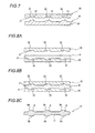
- a molding die 20 illustrated in FIG. 7 is used for molding the shape of one surface of the lens array 10.
- the molding die 20 is fabricated by using the master 40.
- a transfer face 21 of the molding die 20 is formed by transferring the shape of the master 40.
- the transfer face 21 of the molding die 20 is in a shape obtained by reversing the shape of the surface of the lens array 10.
- lens forming faces 22 are two-dimensionally arranged in accordance with the arrangement of the lens parts 6 on the lens array 10.
- Each lens forming face 22 is molded into a concave spherical shape correspondingly to the convex spherical shape of each lens face 6a.
- the molding die 20 is fabricated by, for example, the electrocasting.
- a conducting film is first formed on the surface of the master 40.
- the master 40 thus having the conducting film thereon is immersed in a plating solution, and an electric field is formed in the solution with the conductive film used as an electrode.
- nickel (Ni) is precipitated and deposited on the surface of the master 40.
- a surface of the nickel deposition disposed on the side of the master 40 corresponds to the transfer face 21. The nickel deposition thus obtained is used as the molding die 20.
- a molding die for molding the shape of the front surface and a molding die for molding the shape of the back surface are fabricated through the aforementioned procedures, and the pair of these molding dies are used for fabricating the lens array 10.
- a single master may be commonly used for obtaining two molding dies.
- the molding die 20 fabricated through the aforementioned processes is used as an upper die, and a molding die 30 fabricated through similar processes is used as a lower die.
- a molding material M is supplied onto a transfer face 31 of the lower die 30, so that the molding material M may spread over the transfer face 31.
- the molding material M has comparatively low flowability, for example, the molding material M is preheated for increasing the flowability before supplying it onto the transfer face 31.
- the resin composition with an energy-curing property may be a resin composition cured through heat or a resin composition cured through irradiation with activation energy beams (such as irradiation with UV or electron beams).
- the resin composition preferably has appropriate flowability before the molding from the viewpoint of molding characteristics such as a characteristic to transfer the shape of a molding die.
- a resin composition that is in the form of a liquid at room temperature and has viscosity of approximately 1000 through 50000 mPa ⁇ s is preferably used.
- the resin composition preferably attains, when cured, heat resistance sufficient for avoiding heat distortion even through reflow processing.
- a cured substance of the resin composition has a glass transition temperature of preferably 200°C or more, more preferably 250°C or more and particularly preferably 300°C or more.
- a method in which the crosslink density per unit volume is increased (2) a method in which a resin with a rigid ring system (i.e., a resin having an alicyclic system such as cyclohexane, norbomane or tetracyclododecane, an aromatic ring system such as benzene or naphthalene, a cardo system such as 9,9'-biphenylfluorene or a spiro system such as spirobiindane, and more specifically, a resin disclosed in, for example, JP-A-9-137043 , JP-A-10-67970 , JP-A-2003-55316 , JP-A-2447-334018 or JP-A-2007-238883 ) is used; and (3) a method in which a substance with a
- the resin composition preferably exhibits a small rate of volume shrinkage in the curing reaction.
- the rate of shrinkage of the resin composition caused in the curing is preferably 10% or less, more preferably 5% or less and particularly preferably 3% or less.
- a resin composition including a polymeric curing agent such as a prepolymer (specific examples of which are described in, for example, JP-A- 2001-19740 , JP-A-2004-302293 and JP-A-2007-211247 ;
- a number average molecular weight of the polymeric curing agent is preferably 200 through 100,000, more preferably 500 through 50,000 and particularly preferably 1,000 through 20,000, and a value calculated by dividing the number average molecular weight of the curing agent by the number of curing reactive groups thereof is preferably 50 through 10,000, more preferably 100 through 5,000 and particularly preferably 200 through 3,000);
- a resin composition including a nonreactive substance such as organic/inorganic particulates or a nonreactive resin
- a resin composition including a nonreactive substance such as organic/inorganic particulates or a nonreactive resin
- compositions with a small rate of shrinkage caused in the curing are preferably combined for use (for example, a resin composition including the prepolymer having a ring opening polymerizable group and the particulates is used).
- a resin having a larger Abbe number has an Abbe number (vd) of preferably 50 or more, more preferably 55 or more and particularly preferably 60 or more.
- the refractive index (nd) of such a resin is preferably 1.52 or more, more preferably 1.55 or more and particularly preferably 1.57 or more.
- an aliphatic resin is preferably used, and a resin of an alicyclic system (i.e., a resin having a ring system such as cyclohexane, norbornane, adamantane, tricyclodecane or tetracyclododecane, specific examples of which are described in, for example, JP-A-10-152551 , JP-A-2002-212500 , JP-A-2003-20334 , JP-A-2004-210932 , JP-A-2006-199790 , JP-A-2007-2144 , JP-A-2007-284650 and JP-A-2008-105999 ) is particularly preferred.
- a resin of an alicyclic system i.e., a resin having a ring system such as cyclohexane, norbornane, adamantane, tricyclodecane or tetracyclododecane, specific examples of which are described in,
- a resin having a smaller Abbe number has an Abbe number (vd) of preferably 30 or less, more preferably 25 or less and particularly preferably 20 or less.
- the refractive index (nd) of such a resin is preferably 1.60 or more, more preferably 1.63 or more and particularly preferably 1.65 or more.
- a resin of an aromatic system is preferably used, and for example, a resin having a system of 9,9'-diarylfluorene, naphthalene, benzothiazole, benzotriazole or the like (specific examples of which are described in, for example, JP-A-60-38411 , JP-A-10-67977 , JP-A-2002-47335 , JP-A-2003-238884 , JP-A-2004-83855 , TP-A-2005-325331 and JP-A-2007-238883 , WO-A-2006/095610 and JP-B-2537540 ) is preferably used.
- the resin composition preferably includes inorganic particulates dispersed in a matrix.
- the inorganic particulates are oxide particulates, sulfide particulates, selenide particulates and telluride particulates. More specific examples are particulates of zirconium oxide, titanium oxide, zinc oxide, tin oxide, niobium oxide, cerium oxide, aluminum oxide, lanthanum oxide, yttrium oxide, zinc sulfide and the like.
- particulates of lanthanum oxide, aluminum oxide, zirconium oxide or the like are preferably dispersed, and in the resin having a lower Abbe number, particulates of titanium oxide, tin oxide, zirconium oxide or the like are preferably dispersed.
- one kind of these inorganic particulates may be singly used or two or more kinds of them may be used together.
- particulates of a composite including a plurality of components may be used.
- the inorganic particulates may be doped with a different kind of metal, coated with a different metal oxide such as silica or alumina on their surface layers, or subjected to surface modification with a silane coupling agent, a titanate coupling agent, an organic acid (such as a carboxylic acid, a sulfonic acid, a phosphoric acid or a phosphonic acid) or a dispersing agent having an organic acid group.
- the number average primary particle size of the inorganic particulates may be generally approximately 1 nm through 1000 nm, and when it is too small, the properties of the substance may be changed, and when it is too large, the influence of Rayleigh scattering may be largely exhibited, and therefore, the number average primary particle size is preferably 1 nm through 15 nm, more preferably 2 nm through 10 nm and particularly preferably 3 nm through 7 nm. Moreover, the particle size distribution of the inorganic particulates is preferably as small as possible. In this manner, monodisperse particulates may be variously defined, and for example, a numerically specified range described in JP-A-2006-160992 corresponds to a preferable particle size distribution.
- the aforementioned number average primary particle size may be measured with, for example, an X-ray diffractometer (XRD), a transmission electron microscope (TEM) or the like.
- the refractive index of the inorganic particulates at 22°C and a wavelength of 589 nm is preferably 1.90 through 3.00, more preferably 1.90 through 2.70 and particularly preferably 2.00 through 2.70.
- the content of the inorganic particulates in the resin is preferably 5 mass% or more, more preferably 10 through 70 mass% and particularly preferably 30 through 60 mass% from the viewpoint of transparency and improvement in the refractive index.
- the particulates are dispersed preferably by appropriately using, for example, a dispersing agent including a functional group with reactivity with a resin monomer forming the matrix (described in, for example, an embodiment of JP-A-2007-238884 ), a block copolymer including a hydrophobic chain segment and a hydrophilic chain segment (described in, for example, JP-A-2007-211164 ), a resin having, in a terminal or a side chain of a high polymer molecule, a functional group capable of forming an arbitrary chemical bond with the inorganic particulate (described in, for example, JP-A-2007-238929 and JP-A-2007-238930 ) or the like.
- a dispersing agent including a functional group with reactivity with a resin monomer forming the matrix described in, for example, an embodiment of JP-A-2007-238884
- the resin composition may appropriately include a known releasing agent such as a silicon-based, a fluorine-based or a long-chain alkyl group-containing compound or an additive such as an antioxidant like hindered phenol or the like.
- a known releasing agent such as a silicon-based, a fluorine-based or a long-chain alkyl group-containing compound or an additive such as an antioxidant like hindered phenol or the like.
- the resin composition may include a curing catalyst or an initiator if necessary.
- a specific example is a compound accelerating a curing reaction (i.e., radical polymerization or ion polymerization) through the function of heat or activation energy beams described in, for example, JP-A-2005-92099 (in paragraphs [0063] through [0070]).
- the content of such a curing reaction accelerator depends upon the type of catalyst or initiator or the site with curing reactivity and may not be unconditionally specified but, in general, the content is preferably approximately 0.1 through 15 mass% and more preferably approximately 0.5 through 5 mass% on the basis of the total solid content of the curing reactive resin composition.
- the resin composition may be fabricated by appropriately mixing the aforementioned components.
- the other components may be dissolved in a liquid low-molecular monomer (i.e., a reactive diluent)
- a solvent there is no need to separately add a solvent.
- the curable resin composition may be fabricated by dissolving the components by using a solvent.
- the solvent to be used for the curable resin composition is not particularly specified but may be appropriately selected as far as the resin composition may be homogeneously dissolved or dispersed therein without precipitating, and specific examples are ketones (such as acetone, methyl ethyl ketone or methyl isobutyl ketone), esters (such as ethyl acetate or butyl acetate), ethers (such as tetrahydrofuran or 1,4-dioxane), alcohols (such as methanol, ethanol, isopropyl alcohol, butanol or ethylene glycol), aromatic carbon hydroxides (such as toluene or xylene) and water.
- the shape of the molding die is transferred preferably after casting the composition onto a substrate and/or a die and drying the solvent.
- the upper die 20 is lowered, and the molding material M is deformed in accordance with the shapes of the transfer faces 21 and 31 by sandwiching and pressing the molding material M between the transfer face 21 of the upper die 20 and the transfer face 31 of the lower die 30.
- the molding material M is provided with curing energy by heating it or irradiating it with the activation energy beams so as to cure the molding material M between the transfer face 21 of the upper die 20 and the transfer face 31 of the lower die 30, and thus, the lens array 10 is obtained.
- the lens part 6 is molded between the lens forming face 22 of the upper 20 and a lens forming face 32 of the lowered die 30 paired with each other.
- the substrate part 11 is molded between the transfer face 21 of the upper die 20 and the transfer face 31 of the lower die 30 excluding the lens forming faces 22 and 32.
- the lens array 10 is released from the upper die 20 and the lower die 30 as illustrated in FIG. 8C .
- the resin supplied onto the master substrate is cured in two steps of first curing processing performed through the irradiation with UV and second curing processing performed by supply heat, but the process for curing the resin is not limited to this.
- FIGS. 9A through 9D illustrate a modification of the fabrication procedures for the master of FIGS. 6A through 6D .
- a resin 60 used in this modification is a resin with a UV-curing property and a thermosetting property, and is cured to some extent by supplying heat and completely cured further through irradiation with UV.
- the resin 60 is supplied onto the master substrate 61 by using a dispenser 50 as illustrated in FIG. 9A .
- the resin 60 is supplied onto the master substrate 61 in a prescribed amount in each of a plurality of positions disposed at constant intervals.
- the resin 60 After supplying the resin 60, heat H is supplied to all the portions of the resin 60 provided on the master substrate 61 as illustrated in FIG. 9B .
- the resin 60 is cured up to a quasi-cured state, that is, a cured state where the resin 60 may be deformed by applying a pressure in subsequent molding processing and the deformed shape of the resin 60 may be retained (first curing processing).
- the heat H is simultaneously supplied to all the portions of the resin 60 disposed in the plural positions on the master substrate 61 so as to cure them as a whole up to the quasi-cured state.
- the resin 60 has viscosity of 10 2 through 10 5 Pa ⁇ s in the quasi-cured state.
- the resin 60 is molded by using the master molding die 70 as illustrated in FIG. 9C , so as to form a lens shape face 42 on the master substrate 61.
- lens shape faces 42 in the same number as the lens parts 6 of the lens array 10 are formed on the surface of the master substrate 61.
- the lens shape faces 42 in the prescribed number formed on the master substrate 61 are simultaneously irradiated with UV L as illustrated in FIG. 9D , so as to completely cure the resin 60 including the lens shape faces 42 and a flat portion disposed around the lens shape faces 42 (second curing processing).
- the master 40 is obtained.
- FIGS. 10A through 10D illustrate another modification of the fabrication procedures for the master of FIGS. 6A through 6D .
- a resin 60 used in this modification is a thermosetting resin, and is cured to some extent by supplying heat and completely cured by further supplying heat.
- the resin 60 is supplied onto the master substrate 61 by using a dispenser 50 as illustrated in FIG. 10A .
- the resin 60 is supplied onto the master substrate 61 in a prescribed amount in each of a plurality of positions disposed at constant intervals.
- the resin 60 After supplying the resin 60, heat H is supplied to all the portions of the resin 60 provided on the master substrate 61 as illustrated in FIG. 10B .
- the resin 60 is cured up to a quasi-cured state, that is, a cured state where the resin 60 may be deformed by applying a pressure in subsequent molding processing and the deformed shape of the resin 60 may be retained (first curing processing).
- the heat H is simultaneously supplied to all the portions the resin 60 disposed in the plural positions on the master substrate 61 so as to cure them as a whole up to the quasi-cured state.
- the resin 60 has viscosity of 10 2 through 10 6 Pa ⁇ s in the quasi-cured state.
- the resin 60 is molded by using the master molding die 70 as illustrated in FIG. 10C , so as to form a lens shape face 42 on the master substrate 61.
- lens shape faces 42 in the same number as the lens parts 6 of the lens array 10 are formed on the surface of the master substrate 61.
- the heat H is simultaneously supplied to the lens shape faces 42 in the prescribed number formed on the master substrate 61 as illustrated in FIG. 10D , so as to completely cure the resin 60 including the lens shape faces 42 and a flat portion disposed around the lens shape faces 42 (second curing processing).
- the master 40 is obtained.
- the resin is cured by heating both in the first curing processing, and the second curing processing.
- a temperature T1 at which the resin is cured in the first curing processing is preferably lower than a temperature T2 at which the resin is cured in the second curing processing.
- a curing degree of the resin attained through heating depends upon the heating time, and hence is controlled in the first curing processing in accordance with a product of a heating time t1 and the curing temperature T2.
- FIGS. 11A through 11D illustrate another modification of the fabrication procedures for the master of FIGS. 6A through 6D .
- a resin 60 used in this modification is a UV-curing resin, and is cured to some extent through irradiation with UV and completely cured further through irradiation with UV
- the resin 60 is supplied onto the master substrate 61 by using a dispenser 50 as illustrated in FIG. 11A .
- the resin 60 is supplied onto the master substrate 61 in a prescribed amount in each of a plurality of positions disposed at constant intervals.
- UV L is supplied to all the portions of the resin 60 provided on the master substrate 61 as illustrated in FIG. 11B .
- the resin 60 is cured up to a quasi-cured state, that is, a cured state where the resin 60 may be deformed by applying a pressure in subsequent molding processing and the deformed shape of the resin 60 may be retained (first curing processing).
- the UV L is simultaneously supplied to all the portions of the resin 60 disposed in the plural positions on the master substrate G1 so as to cure them as a whole up to the quasi-cured state.
- the resin 60 has viscosity of 10 2 through 10 6 Pa ⁇ s in the quasi-cured state.
- the resin 60 is molded by using the master molding die 70 as illustrated in FIG. 11C , so as to form a lens shape face 42 on the master substrate 61.
- lens shape faces 42 in the same number as the lens parts 6 of the lens array 10 are formed on the surface of the master substrate 61.
- the lens shape faces 42 in the prescribed number formed on the master substrate 61 are simultaneously irradiated with UV L as illustrated in FIG. 11D , so as to completely cure the resin 60 including the lens shape faces 42 and a flat portion disposed around the lens shape faces 42 (second curing processing).
- the master 40 is obtained.
- the resin is cured through the UV irradiation in both the first curing processing and the second curing processing.
- UV output is P1
- an irradiation time is tp1 and a curing temperature is T1 in curing the resin in the first curing processing and that UV output is P2
- an irradiation time is tp2 and a curing temperature is T2 in curing the resin in the second curing processing
- the irradiation time may be advantageously suppressed to be minimum, which is preferred because the fabrication efficiency is thus improved.
- a preferable resin composition includes monomers having different reactivity, such as a combination of a ring opening polymerizable monomer (such as an epoxy group-containing monomer) and a radial polymerizable monomer (such as (meth)acryloyl group-containing monomer), a curing assistant for accelerating a reaction of one of the monomers through a function of light or heat and a curing assistant for accelerating a reaction of the other monomer through a function of different energy (which difference includes not only a difference between the light and the heat but also a difference in a light irradiation wavelength, a heating temperature or the like).
- a ring opening polymerizable monomer such as an epoxy group-containing monomer
- a radial polymerizable monomer such as (meth)acryloyl group-containing monomer
- a curing assistant for accelerating a reaction of one of the monomers through a function of light or heat such as (meth)acryloyl group-containing monomer
- a resin composition including a monomer with a single polymerization property, a curing assistant for accelerating a reaction through a function of heat and a curing assistant for accelerating a reaction through a function of light may be preferably used.
- Examples of the resin composition including monomers with different reactivity are resin compositions described in, for example, JP-A-11-228610 , JP-A-2003-128747 , JP-A-2004-315744 , JP-A-2006-131866 and JP-A-2006-131867 , and JP-A-2009-513 777 .
- resin composition including a monomer with a single polymerization property is a resin composition described in, for example, JF-A-8-258172.
- a curable resin composition was prepared by mixing and dissolving 45 parts by weight of glycidyl methacrylate (brand name: Light-ester G; manufactured by Kyoeisha Chemical Co., Ltd.), 1 part by weight of dipentaerythritol hexacrylate (manufactured by Aldrich), 50 parts by weight of alicyclic anhydride (brand name: Rikacid HNA-100; manufactured by New Japan Chemical Co., Ltd.), 1 part by weight of a photoradical polymerization initiator (brand name: Irgacure 184; manufactured by Ciba Specialty Chemicals), and 3 parts by weight of thermionic polymerization initiator (brand name: Alicart 336; manufactured by Aldrich).
- glycidyl methacrylate brand name: Light-ester G; manufactured by Kyoeisha Chemical Co., Ltd.
- dipentaerythritol hexacrylate manufactured by Aldrich
- alicyclic anhydride brand name:
- a curable resin composition B was prepared by mixing and dissolving 45 parts by weight of glycidyl methacrylate (brand name: Light-ester G; manufactured by Kyoeisha Chemical Co., Ltd.), 1 part by weight of dipentaerythritol hexacrylate (manufactured by Aldrich), 50 parts by weight of alicyclic anhydride (brand name: Rikacid HNA-100; manufactured by New Japan Chemical Co., Ltd.), 1 part by weight of thermoradical polymerization initiator (brand name: Perocta ND; manufactured by NOF Corporation), and 3 parts by weight of a thermionic polymerization initiator (brand name: Alicart 336; manufactured by Aldrich).
- glycidyl methacrylate brand name: Light-ester G; manufactured by Kyoeisha Chemical Co., Ltd.
- dipentaerythritol hexacrylate manufactured by Aldrich
- alicyclic anhydride brand name: Rikacid HNA-
- a curable resin composition C was prepared by mixing and dissolving 85.5 parts by weight of 3,4-epoxycyclohexyl methyl methacrylate (brand name: Cyclomer M-100; manufactured by Daicel Chemical Industries, Ltd.), 0.5 part by weight of dipentaerythritol hexacrylate (manufactured by Aldrich), 10 parts by weight of 3,4-epoxycyclohexyl methyl-3',4'-epoxycyclohexane carboxylate (brand name: Celoxide 2021P; manufactured by Daicel Chemical Industries, Ltd.), 2 parts by weight of thermoradical polymerization initiator (brand name: Perocta ND; manufactured by NOF Corporation), and 3 parts by weight of triaryl sulfonium hexafluoroantimonate (brand name: UV-6974; manufactured by Union Carbide Corporation).
- brand name: Cyclomer M-100 manufactured by Daicel Chemical Industries, Ltd.
- the curing temperature was set to 120°C and the heating time was set to 2 minutes for supplying heat in the first curing processing, and a high-pressure mercury lamp was used as a light source for performing irradiation at an integrated exposure of 3000 mJ/cm 2 in the second curing processing. Furthermore, post-curing at 100°C for 2 hours (namely, post-heating at 100°C for 2 hours for sufficiently completing the curing reaction) is preferably performed.
- the exemplary embodiments disclose the following method.
- the method for fabricating a lens array described so far is applicable to fabrication of an imaging lens provided in an imaging part of a digital camera, an endoscope, portable electronic equipment or the like.
Landscapes
- Engineering & Computer Science (AREA)
- Mechanical Engineering (AREA)
- Manufacturing & Machinery (AREA)
- Health & Medical Sciences (AREA)
- Ophthalmology & Optometry (AREA)
- Physics & Mathematics (AREA)
- General Physics & Mathematics (AREA)
- Optics & Photonics (AREA)
- Moulds For Moulding Plastics Or The Like (AREA)
- Casting Or Compression Moulding Of Plastics Or The Like (AREA)
- Solid State Image Pick-Up Elements (AREA)
Abstract
Description
- The present invention relates to a method for fabricating a master to be used in fabrication of a molding die.
- Recently, a portable terminal such as a cellular phone or a PDA (Personal Digital Assistant) includes a compact and thin imaging unit. Such an imaging unit generally includes a solid state imaging device such as a CCD (Charge Coupled Device) image sensor or a CMOS (Complementary Metal-Oxide Semiconductor) image sensor and a lens for forming an object image on the solid state imaging device.
- In order that lenses packaged in such imaging units may be inexpensively mass-produced for reducing the cost of the imaging units, there is a demand for improvement of efficiency in the fabrication of lenses. As a method for fabricating lenses employed for this purpose, in known mass production of lenses to be packaged in the imaging units, a lens array including a plurality of lens parts formed in a substrate part is fabricated and the plural lens parts are separated from one another by cutting the substrate part.
- As a method for fabricating the lens array, a fabrication method including the following procedures is known (see Patent Document 1(
JP-B-4226067 - (1) A die having a lens forming face in a shape obtained by reversing a desired lens face shape is used for transferring the lens forming shape of the die onto a resin supplied to the front surface of a substrate, and the resin is cured.
- (2) The procedure (1) is repeated, so as to arrange, on the surface of the substrate, resin molding parts molded into the lens face shape.
- (3) In the same manner, the resin molding parts molded into the lens face shape are arranged also on the back surface of the substrate, so as to obtain a master.
- (4) A metal such as Ni is deposited through electrocasting onto the both surfaces of the master, so as to obtain an upper die and a lower die.
- (5) A photo-curing resin material or a thermosetting resin material is supplied between the upper die and the lower die.
- (6) The resin material is sandwiched and pressed between the upper die and the lower die, so as to deform the resin material in accordance with the shapes of the dies.
- (7) The resin material is irradiated with light or heated, so as to cure the resin material.
- Patent Document 1 describes a method for fabricating a master to be used for obtaining a molding die for use in molding of an optical device array in which a photo-curing resin is injected into a plurality of holes formed on a wafer, respective portions of the photo-curing resin thus injected into the plural holes are successively molded by using a transfer body, and the photo-curing resin is cured through irradiation with light while in contact with the transfer body.
- According to the method described in Patent Document 1, however, the operations of molding the resin, curing the resin with light and moving the master molding die are repeatedly performed through step-and-repeat processing in the fabrication of the master, and hence, the fabrication efficiency is poor.
- The present invention provides a method for fabricating a master attaining improved fabrication efficiency.
- According to an aspect of the present invention, a method for fabricating a master for use in fabrication of a molding die to be used in molding of a molded body having a plurality of molding parts arranged thereon, includes: a resin supplying step of supplying a resin onto a master substrate; a first curing step of curing the supplied resin as a whole up to a quasi-cured state corresponding to a cured state where the resin may be deformed at a pressure applied in the molding and may retain a deformed shape thereof; a molding step of transferring, onto the resin, a plane in the same shape as molding faces of the molding parts by using a master molding die after the first curing step; and a second curing step of further curing the resin after the molding step.
- With the configuration of the aspect of the present invention, after a resin is supplied onto a master substrate, the resin is molded as a whole by curing it up to a quasi-cured state. The resin kept in the thus molded shape is completely cured through second curing processing, so as to obtain a master. In this manner, whole portions of the resin disposed in a plurality of positions on the master substrate may be cured through two-step curing processing, and hence, the fabrication efficiency may be improved as compared with the conventional step-and-repeat processing in which the molding and the curing are repeated on the respective portions of the resin supplied to prescribed positions on a master substrate.
- The aspect of the present invention provides a method for fabricating a master in which the fabrication efficiency of the master to be used for fabricating a molding die for use in molding a molded body may be improved.
-
-
FIG. 1 is a cross-sectional view illustrating an exemplary imaging unit used for explaining an embodiment of the invention. -
FIG. 2 is a plan view of an exemplary lens array used for explaining the embodiment of the invention. -
FIG. 3 is a cross-sectional view of the lens array ofFIG 2 taken on line III-III. -
FIG. 4 is a plan view of an exemplary master model used for explaining the embodiment of the invention. -
FIG. 5 is a cross-sectional view of the master model ofFIG. 4 taken on line V-V. -
FIGS. 6A through 6D are schematic diagrams successively illustrating fabrication procedures for the master model ofFIG. 4 . -
FIG. 7 is a cross-sectional view of an exemplary molding die. -
FIGS. 8A through 8C are schematic diagrams successively illustrating fabrication procedures for the lens array ofFIG. 2 . -
FIGS. 9A through 9D are schematic diagrams illustrating a modification of the fabrication procedures for the master model ofFIGS. 6A through 6D . -
FIGS. 10A through 10D are schematic diagrams illustrating another modification of the fabrication procedures for the master model ofFIGS. 6A through 6D . -
FIGS. 11A through 11D are schematic diagrams illustrating another modification of the fabrication procedures for the master model ofFIGS. 6A through 6D . - An imaging unit 1 of
FIG. 1 includes asensor module 2 and alens module 3. - The
sensor module 2 includes a solid state imaging device 4 and asubstrate part 5. Thesubstrate part 5 is made of a semiconductor material such as silicon. The solid state imaging device 4 is, for example, a CCD image sensor or a CMOS image sensor, and is obtained by forming a light receiving region, an insulating film, an electrode, a line and the like on thesubstrate part 5 by repeatedly subjecting thesubstrate part 5 to known filming processing, photolithography processing, etching processing, impurity doping processing and the like. - The
lens module 3 includes alens part 6 and a flange part 7. Thelens part 6 has prescribedlens faces FIG. 1 , and any of various combinations of a convex spherical face, a concave spherical face, an aspherical face and a plane face may be employed in accordance with the application. The flange part 7 projects from the outer circumference of thelens part 6 in the shape of a flange so as to surround the outer circumference of thelens part 6. Thelens part 6 and the flange part 7 are integrally formed from a translucent material. - The
lens module 3 is stacked on and assembled to thesensor module 2 with a spacer 9 disposed between the flange part 7 and thesubstrate part 5. The spacer 9 has a thickness for providing a prescribed distance between thesubstrate part 5 of thesensor module 2 and the flange part 7 of thelens module 3 so that thelens part 6 of thelens module 3 may form an image on a light receiving face of the solid state imaging device 4 of thesensor module 2. The spacer 9 is adhered to themodules - The shape of the spacer 9 is not particularly specified as far as a prescribed distance may be provided between the substrate part of the
sensor module 2 and the flange part 7 of thelens module 3, and the spacer 9 is preferably a frame-shaped member surrounding the solid state imaging device 4 for isolating a space formed between themodules modules modules - Although merely one
sensor module 3 is assembled onto thesensor module 2 in the example ofFIG. 1 , a plurality oflens modules 3 may be assembled. In such a case, a plurality oflens modules 3 are successively stacked with spacers similar to the spacer 9 sandwiched therebetween to be assembled onto thesensor module 2. Furthermore, the lens faces 6a and 6b of thelens parts 6 of theselens modules 3 may be different among therespective lens modules 3. - The imaging unit 1 having this structure is mounted through reflow on a circuit substrate of, for example, a portable terminal. A paste solder is precedently printed on the circuit substrate in a position for mounting the imaging unit 1, and the imaging unit 1 is placed thereon. Then, the circuit substrate including the imaging unit 1 is subjected to irradiation with infrared or annealing with hot air blow. Through this processing, the solder is molten, so as to mount the imaging unit 1 onto the circuit substrate.
- The
aforementioned lens module 3 is obtained by cutting a lens array, in which a plurality oflens parts 6 are one-dimensionally or two-dimensionally arranged, into pieces each including onelens part 6. Also, thesensor module 2 is similarly obtained by cutting a sensor array, in which a plurality of solid state imaging devices are one-dimensionally or two-dimensionally arranged, into pieces each including one solid state imaging device. Now, the lens array used for obtaining thelens module 3 will be described. - A
lens array 10 illustrated inFIGS. 2 and3 includes a plurality oflens parts 6 and asubstrate part 11 connecting theselens parts 6 to one another. Thelens array 10 is designated also as a wafer-level lens array in the shape of a wafer with a prescribed size as a whole and including a plurality oflens parts 6 arranged thereon, and in an example illustrated in these drawings, theplural lens parts 6 are two-dimensionally arranged. Theselens parts 6 and thesubstrate part 11 are integrally formed from a translucent material. - The aforementioned lens module 3 (illustrated in
FIG. 1 ) is obtained by cutting thesubstrate part 11 of thelens array 10 in portions disposed betweenadjacent lens parts 6. A portion of thesubstrate part 11 thus cut to remain on eachlens part 6 corresponds to the flange part 7 of thelens module 3. - Next, an exemplary fabrication method for the
lens array 10 will be described. In the following fabrication method for thelens array 10, a master model (hereinafter simply referred to as the master) of the lens array is first fabricated, and a molding die is obtained from this master. Thereafter, thelens array 10 is fabricated by using the molding die. - A
master 40 illustrated inFIGS. 4 and5 has a surface in the same shape as the surface of thelens array 10. Themaster 40 includes asubstrate 41. Thesubstrate 41 is made of a material having glass transition (with a glass transition point Tg1), such as glass or a resin, and is formed in the shape of a wafer with the same size as thelens array 10. On the surface of thesubstrate 41, lens shape faces 42 are two-dimensionally arranged in accordance with the arrangement of thelens parts 6 on thelens array 10. Each lens shape face 42 is in the same shape as eachlens face 6a formed on the front surface of thelens part 6 of thelens array 10. - A method for fabricating the
master 40 will now be described with reference toFIGS. 6A through 6D . - First, a
resin 60 is supplied onto amaster substrate 61 by using adispenser 50 as illustrated inFIG. 6A . Theresin 60 is supplied onto themaster substrate 61 in a prescribed amount in each of a plurality of positions disposed at constant intervals. - In this exemplary case, the
resin 60 is a resin with a UV curing property and a thermosetting property, and is cured to some extent through irradiation with UV and completely cured further by supplying heat. - After supplying the
resin 60, all the portions of the resin supplied onto themaster substrate 61 are irradiated with UV L as illustrated inFIG. 6B . Thus, theresin 60 is cured up to a quasi-cured state, that is, a cured state where theresin 60 may be deformed by applying a pressure in subsequent molding processing and the deformed shape of theresin 60 may be retained (first curing processing). At this point, all the portions of theresin 60 supplied to the plural positions on themaster substrate 61 are simultaneously irradiated with the UV L and are cured as a whole. Theresin 60 has viscosity of 102 through 106 Pa·s in the quasi-cured state. - After curing the
resin 60 up to the quasi-cured state, theresin 60 is molded by using a master molding die 70 as illustrated inFIG. 6C . The master molding die has alens molding face 70a for transferring a face in the same shape as thelens face FIG. 1 ). When the master molding die 70 is pressed against theresin 60, theresin 60 is deformed in accordance with the shape of thelens molding face 70a. In this manner, a lens shape face 42 is formed on themaster substrate 61. Such transfer using the master molding die 70 is repeated, and lens shape faces 42 in the same number as thelens parts 6 of thelens array 10 are formed on the surface of themaster substrate 61. - After repeating the transfer using the master molding die 70 by a prescribed number of times, the lens shape faces 42 in the prescribed number formed on the
master substrate 61 are heated as a whole, as illustrated inFIG. 6D , and thus, theresin 60 including the lens shape faces 42 and a flat portion disposed around the lens shape faces 42 is completely cured (second curing processing). In this manner, themaster 40 is obtained. - As described above, after supplying the
resin 60 onto themaster substrate 41, theresin 60 is cured up to the quasi-cured state as a whole, and thereafter, the resin is molded by using the master molding die. Subsequently, theresin 60 retaining the molded shape is completely cured through the second curing processing, so as to give themaster 40. Therefore, all the portions of theresin 60 disposed in a plurality of positions on themaster substrate 41 may be cured through two-step curing processing, and hence, the fabrication efficiency may be improved as compared with the conventional step-and-repeat processing in which the molding and the curing are repeated on respective portions of a resin supplied in prescribed positions on themaster substrate 41. - Next, a molding die for the
lens array 10 will be described. - A molding die 20 illustrated in
FIG. 7 is used for molding the shape of one surface of thelens array 10. The molding die 20 is fabricated by using themaster 40. - A
transfer face 21 of the molding die 20 is formed by transferring the shape of themaster 40. In other words, thetransfer face 21 of the molding die 20 is in a shape obtained by reversing the shape of the surface of thelens array 10. On thetransfer face 21, lens forming faces 22 are two-dimensionally arranged in accordance with the arrangement of thelens parts 6 on thelens array 10. Eachlens forming face 22 is molded into a concave spherical shape correspondingly to the convex spherical shape of eachlens face 6a. - The molding die 20 is fabricated by, for example, the electrocasting. In the fabrication of the molding die by the electrocasting, a conducting film is first formed on the surface of the
master 40. Themaster 40 thus having the conducting film thereon is immersed in a plating solution, and an electric field is formed in the solution with the conductive film used as an electrode. In this manner, nickel (Ni) is precipitated and deposited on the surface of themaster 40. A surface of the nickel deposition disposed on the side of themaster 40 corresponds to thetransfer face 21. The nickel deposition thus obtained is used as the molding die 20. - When a molded body has lens parts on the both surfaces as the
lens array 10 ofFIG. 3 , a molding die for molding the shape of the front surface and a molding die for molding the shape of the back surface are fabricated through the aforementioned procedures, and the pair of these molding dies are used for fabricating thelens array 10. Incidentally, when the arrangement and the shape of the lens parts are the same on the both surfaces of thelens array 10, a single master may be commonly used for obtaining two molding dies. - Next, a method for fabricating a lens array by using a molding die fabricated through the aforementioned processes will be described.
- In an example described below, the molding die 20 fabricated through the aforementioned processes is used as an upper die, and a
molding die 30 fabricated through similar processes is used as a lower die. - First, as illustrated in
FIG. 8A , a molding material M is supplied onto atransfer face 31 of thelower die 30, so that the molding material M may spread over thetransfer face 31. When the molding material M has comparatively low flowability, for example, the molding material M is preheated for increasing the flowability before supplying it onto thetransfer face 31. - As the molding material M, a resin composition with an energy-curing property may be used. The resin composition with an energy-curing property may be a resin composition cured through heat or a resin composition cured through irradiation with activation energy beams (such as irradiation with UV or electron beams).
- The resin composition preferably has appropriate flowability before the molding from the viewpoint of molding characteristics such as a characteristic to transfer the shape of a molding die. Specifically, a resin composition that is in the form of a liquid at room temperature and has viscosity of approximately 1000 through 50000 mPa·s is preferably used.
- On the other hand, the resin composition preferably attains, when cured, heat resistance sufficient for avoiding heat distortion even through reflow processing. From this point of view, a cured substance of the resin composition has a glass transition temperature of preferably 200°C or more, more preferably 250°C or more and particularly preferably 300°C or more. In order to provide a resin composition with such high heat resistance, it is necessary to constrain mobility on the level of molecules, and examples of effective methods to be employed for this purpose are as follows: (1) A method in which the crosslink density per unit volume is increased; (2) a method in which a resin with a rigid ring system (i.e., a resin having an alicyclic system such as cyclohexane, norbomane or tetracyclododecane, an aromatic ring system such as benzene or naphthalene, a cardo system such as 9,9'-biphenylfluorene or a spiro system such as spirobiindane, and more specifically, a resin disclosed in, for example,
JP-A-9-137043 JP-A-10-67970 JP-A-2003-55316 JP-A-2447-334018 JP-A-2007-238883 JP-A-5-209027 JP-A-10-298265 - From the viewpoint of accuracy in transferring a shape, the resin composition preferably exhibits a small rate of volume shrinkage in the curing reaction. The rate of shrinkage of the resin composition caused in the curing is preferably 10% or less, more preferably 5% or less and particularly preferably 3% or less. Examples of the resin composition with a small rate of shrinkage caused in the curing are as follows: (1) A resin composition including a polymeric curing agent (such as a prepolymer) (specific examples of which are described in, for example,
JP-A- 2001-19740 JP-A-2004-302293 JP-A-2007-211247 JP-A-6-298883 JP-A-2001-247793 JP-A-2006-225434 JP-A-2004-210932 JP-A-8-134405 JP-A-2002-105110 JP-A-7-62065 JP-A-2003-20334 JP-A-2005-15666 JP-A-9-137043 JP-A-2006-131868 JP-A-2004-2719 JP-A-2008-238417 - Furthermore, different resins respectively having at least two kinds of, namely, larger and smaller, Abbe numbers are preferably used. A resin having a larger Abbe number has an Abbe number (vd) of preferably 50 or more, more preferably 55 or more and particularly preferably 60 or more. The refractive index (nd) of such a resin is preferably 1.52 or more, more preferably 1.55 or more and particularly preferably 1.57 or more. As such a resin, an aliphatic resin is preferably used, and a resin of an alicyclic system (i.e., a resin having a ring system such as cyclohexane, norbornane, adamantane, tricyclodecane or tetracyclododecane, specific examples of which are described in, for example,
JP-A-10-152551 JP-A-2002-212500 JP-A-2003-20334 JP-A-2004-210932 JP-A-2006-199790 JP-A-2007-2144 JP-A-2007-284650 JP-A-2008-105999 - A resin having a smaller Abbe number has an Abbe number (vd) of preferably 30 or less, more preferably 25 or less and particularly preferably 20 or less. The refractive index (nd) of such a resin is preferably 1.60 or more, more preferably 1.63 or more and particularly preferably 1.65 or more. As such a resin, a resin of an aromatic system is preferably used, and for example, a resin having a system of 9,9'-diarylfluorene, naphthalene, benzothiazole, benzotriazole or the like (specific examples of which are described in, for example,
JP-A-60-38411 JP-A-10-67977 JP-A-2002-47335 JP-A-2003-238884 JP-A-2004-83855 TP-A-2005-325331 JP-A-2007-238883 WO-A-2006/095610 andJP-B-2537540 - For the purpose of increasing the refractive index or adjusting the Able number, the resin composition preferably includes inorganic particulates dispersed in a matrix. Examples of the inorganic particulates are oxide particulates, sulfide particulates, selenide particulates and telluride particulates. More specific examples are particulates of zirconium oxide, titanium oxide, zinc oxide, tin oxide, niobium oxide, cerium oxide, aluminum oxide, lanthanum oxide, yttrium oxide, zinc sulfide and the like. In particular, in the resin having a larger Abbe number, particulates of lanthanum oxide, aluminum oxide, zirconium oxide or the like are preferably dispersed, and in the resin having a lower Abbe number, particulates of titanium oxide, tin oxide, zirconium oxide or the like are preferably dispersed. One kind of these inorganic particulates may be singly used or two or more kinds of them may be used together. Alternatively, particulates of a composite including a plurality of components may be used. Furthermore, for various purposes of reducing photocatalytic activity, reducing water absorption and the like, the inorganic particulates may be doped with a different kind of metal, coated with a different metal oxide such as silica or alumina on their surface layers, or subjected to surface modification with a silane coupling agent, a titanate coupling agent, an organic acid (such as a carboxylic acid, a sulfonic acid, a phosphoric acid or a phosphonic acid) or a dispersing agent having an organic acid group. The number average primary particle size of the inorganic particulates may be generally approximately 1 nm through 1000 nm, and when it is too small, the properties of the substance may be changed, and when it is too large, the influence of Rayleigh scattering may be largely exhibited, and therefore, the number average primary particle size is preferably 1 nm through 15 nm, more preferably 2 nm through 10 nm and particularly preferably 3 nm through 7 nm. Moreover, the particle size distribution of the inorganic particulates is preferably as small as possible. In this manner, monodisperse particulates may be variously defined, and for example, a numerically specified range described in
JP-A-2006-160992 - In order to homogeneously disperse the particulates in the resin composition, the particulates are dispersed preferably by appropriately using, for example, a dispersing agent including a functional group with reactivity with a resin monomer forming the matrix (described in, for example, an embodiment of
JP-A-2007-238884 JP-A-2007-211164 JP-A-2007-238929 JP-A-2007-238930 - Furthermore, the resin composition may appropriately include a known releasing agent such as a silicon-based, a fluorine-based or a long-chain alkyl group-containing compound or an additive such as an antioxidant like hindered phenol or the like.
- The resin composition may include a curing catalyst or an initiator if necessary. A specific example is a compound accelerating a curing reaction (i.e., radical polymerization or ion polymerization) through the function of heat or activation energy beams described in, for example,
JP-A-2005-92099 - The resin composition may be fabricated by appropriately mixing the aforementioned components. At this point, in the case where the other components may be dissolved in a liquid low-molecular monomer (i.e., a reactive diluent), there is no need to separately add a solvent. In the other cases, however, the curable resin composition may be fabricated by dissolving the components by using a solvent. The solvent to be used for the curable resin composition is not particularly specified but may be appropriately selected as far as the resin composition may be homogeneously dissolved or dispersed therein without precipitating, and specific examples are ketones (such as acetone, methyl ethyl ketone or methyl isobutyl ketone), esters (such as ethyl acetate or butyl acetate), ethers (such as tetrahydrofuran or 1,4-dioxane), alcohols (such as methanol, ethanol, isopropyl alcohol, butanol or ethylene glycol), aromatic carbon hydroxides (such as toluene or xylene) and water. When the curable resin composition includes the solvent, the shape of the molding die is transferred preferably after casting the composition onto a substrate and/or a die and drying the solvent.
- Subsequently, as illustrated in
FIG. 8B , theupper die 20 is lowered, and the molding material M is deformed in accordance with the shapes of the transfer faces 21 and 31 by sandwiching and pressing the molding material M between thetransfer face 21 of theupper die 20 and thetransfer face 31 of thelower die 30. - Thereafter, after completely lowering the
upper die 20, the molding material M is provided with curing energy by heating it or irradiating it with the activation energy beams so as to cure the molding material M between thetransfer face 21 of theupper die 20 and thetransfer face 31 of thelower die 30, and thus, thelens array 10 is obtained. Thelens part 6 is molded between thelens forming face 22 of the upper 20 and alens forming face 32 of the lowered die 30 paired with each other. Furthermore, thesubstrate part 11 is molded between thetransfer face 21 of theupper die 20 and thetransfer face 31 of thelower die 30 excluding the lens forming faces 22 and 32. - Then, the
lens array 10 is released from theupper die 20 and thelower die 30 as illustrated inFIG. 8C . - In the aforementioned fabrication process for the master, the resin supplied onto the master substrate is cured in two steps of first curing processing performed through the irradiation with UV and second curing processing performed by supply heat, but the process for curing the resin is not limited to this.
-
FIGS. 9A through 9D illustrate a modification of the fabrication procedures for the master ofFIGS. 6A through 6D . Aresin 60 used in this modification is a resin with a UV-curing property and a thermosetting property, and is cured to some extent by supplying heat and completely cured further through irradiation with UV. - First, the
resin 60 is supplied onto themaster substrate 61 by using adispenser 50 as illustrated inFIG. 9A . Theresin 60 is supplied onto themaster substrate 61 in a prescribed amount in each of a plurality of positions disposed at constant intervals. - After supplying the
resin 60, heat H is supplied to all the portions of theresin 60 provided on themaster substrate 61 as illustrated inFIG. 9B . Thus, theresin 60 is cured up to a quasi-cured state, that is, a cured state where theresin 60 may be deformed by applying a pressure in subsequent molding processing and the deformed shape of theresin 60 may be retained (first curing processing). At this point, the heat H is simultaneously supplied to all the portions of theresin 60 disposed in the plural positions on themaster substrate 61 so as to cure them as a whole up to the quasi-cured state. Theresin 60 has viscosity of 102 through 105 Pa·s in the quasi-cured state. - After curing the
resin 60 up to the quasi-cured state, theresin 60 is molded by using the master molding die 70 as illustrated inFIG. 9C , so as to form a lens shape face 42 on themaster substrate 61. By repeating the transfer using the master molding die 70, lens shape faces 42 in the same number as thelens parts 6 of thelens array 10 are formed on the surface of themaster substrate 61. - After repeating the transfer using the master molding die 70 by a prescribed number of times, the lens shape faces 42 in the prescribed number formed on the
master substrate 61 are simultaneously irradiated with UV L as illustrated inFIG. 9D , so as to completely cure theresin 60 including the lens shape faces 42 and a flat portion disposed around the lens shape faces 42 (second curing processing). Thus, themaster 40 is obtained. -
FIGS. 10A through 10D illustrate another modification of the fabrication procedures for the master ofFIGS. 6A through 6D . Aresin 60 used in this modification is a thermosetting resin, and is cured to some extent by supplying heat and completely cured by further supplying heat. - First, the
resin 60 is supplied onto themaster substrate 61 by using adispenser 50 as illustrated inFIG. 10A . Theresin 60 is supplied onto themaster substrate 61 in a prescribed amount in each of a plurality of positions disposed at constant intervals. - After supplying the
resin 60, heat H is supplied to all the portions of theresin 60 provided on themaster substrate 61 as illustrated inFIG. 10B . Thus, theresin 60 is cured up to a quasi-cured state, that is, a cured state where theresin 60 may be deformed by applying a pressure in subsequent molding processing and the deformed shape of theresin 60 may be retained (first curing processing). At this point, the heat H is simultaneously supplied to all the portions theresin 60 disposed in the plural positions on themaster substrate 61 so as to cure them as a whole up to the quasi-cured state. Theresin 60 has viscosity of 102 through 106 Pa·s in the quasi-cured state. - After curing the
resin 60 up to the quasi-cured state, theresin 60 is molded by using the master molding die 70 as illustrated inFIG. 10C , so as to form a lens shape face 42 on themaster substrate 61. By repeating the transfer using the master molding die 70, lens shape faces 42 in the same number as thelens parts 6 of thelens array 10 are formed on the surface of themaster substrate 61. - After repeating the transfer using the master molding die 70 by a prescribed number of times, the heat H is simultaneously supplied to the lens shape faces 42 in the prescribed number formed on the
master substrate 61 as illustrated inFIG. 10D , so as to completely cure theresin 60 including the lens shape faces 42 and a flat portion disposed around the lens shape faces 42 (second curing processing). Thus, themaster 40 is obtained. - In this modification, the resin is cured by heating both in the first curing processing, and the second curing processing. A temperature T1 at which the resin is cured in the first curing processing is preferably lower than a temperature T2 at which the resin is cured in the second curing processing. A curing degree of the resin attained through heating (i.e., a degree of polymerization proceeded in the curable material) depends upon the heating time, and hence is controlled in the first curing processing in accordance with a product of a heating time t1 and the curing temperature T2.
-
FIGS. 11A through 11D illustrate another modification of the fabrication procedures for the master ofFIGS. 6A through 6D . Aresin 60 used in this modification is a UV-curing resin, and is cured to some extent through irradiation with UV and completely cured further through irradiation with UV - First, the
resin 60 is supplied onto themaster substrate 61 by using adispenser 50 as illustrated inFIG. 11A . Theresin 60 is supplied onto themaster substrate 61 in a prescribed amount in each of a plurality of positions disposed at constant intervals. - After supplying the
resin 60, UV L is supplied to all the portions of theresin 60 provided on themaster substrate 61 as illustrated inFIG. 11B . Thus, theresin 60 is cured up to a quasi-cured state, that is, a cured state where theresin 60 may be deformed by applying a pressure in subsequent molding processing and the deformed shape of theresin 60 may be retained (first curing processing). At this point, the UV L is simultaneously supplied to all the portions of theresin 60 disposed in the plural positions on the master substrate G1 so as to cure them as a whole up to the quasi-cured state. Theresin 60 has viscosity of 102 through 106 Pa·s in the quasi-cured state. - After curing the
resin 60 up to the quasi-cured state, theresin 60 is molded by using the master molding die 70 as illustrated inFIG. 11C , so as to form a lens shape face 42 on themaster substrate 61. By repeating the transfer using the master molding die 70, lens shape faces 42 in the same number as thelens parts 6 of thelens array 10 are formed on the surface of themaster substrate 61. - After repeating the transfer using the master molding die 70 by a prescribed number of times, the lens shape faces 42 in the prescribed number formed on the
master substrate 61 are simultaneously irradiated with UV L as illustrated inFIG. 11D , so as to completely cure theresin 60 including the lens shape faces 42 and a flat portion disposed around the lens shape faces 42 (second curing processing). Thus, themaster 40 is obtained. - In this modification, the resin is cured through the UV irradiation in both the first curing processing and the second curing processing. Assuming that UV output is P1, an irradiation time is tp1 and a curing temperature is T1 in curing the resin in the first curing processing and that UV output is P2, an irradiation time is tp2 and a curing temperature is T2 in curing the resin in the second curing processing, the following relationship holds:

- At this point, when the UV output P1 employed in the first curing processing is smaller than the UV output P2 employed in the second curing processing, the irradiation time may be advantageously suppressed to be minimum, which is preferred because the fabrication efficiency is thus improved.
- Next, a resin used in the fabrication process for the master to be cured in two steps using at least one of UV and heat will be described.
- A preferable resin composition includes monomers having different reactivity, such as a combination of a ring opening polymerizable monomer (such as an epoxy group-containing monomer) and a radial polymerizable monomer (such as (meth)acryloyl group-containing monomer), a curing assistant for accelerating a reaction of one of the monomers through a function of light or heat and a curing assistant for accelerating a reaction of the other monomer through a function of different energy (which difference includes not only a difference between the light and the heat but also a difference in a light irradiation wavelength, a heating temperature or the like).
- Alternatively, a resin composition including a monomer with a single polymerization property, a curing assistant for accelerating a reaction through a function of heat and a curing assistant for accelerating a reaction through a function of light may be preferably used.
- Examples of the resin composition including monomers with different reactivity are resin compositions described in, for example,
JP-A-11-228610 JP-A-2003-128747 JP-A-2004-315744 JP-A-2006-131866 JP-A-2006-131867 JP-A-2009-513 777 - An example of the resin composition including a monomer with a single polymerization property is a resin composition described in, for example, JF-A-8-258172.
- Examples of the resin composition and a curing reaction caused by using the resin composition will now be exemplarily described. (Example 1 of Resin Composition: Resin composition A curable in two steps of light and heat)
- A curable resin composition was prepared by mixing and dissolving 45 parts by weight of glycidyl methacrylate (brand name: Light-ester G; manufactured by Kyoeisha Chemical Co., Ltd.), 1 part by weight of dipentaerythritol hexacrylate (manufactured by Aldrich), 50 parts by weight of alicyclic anhydride (brand name: Rikacid HNA-100; manufactured by New Japan Chemical Co., Ltd.), 1 part by weight of a photoradical polymerization initiator (brand name: Irgacure 184; manufactured by Ciba Specialty Chemicals), and 3 parts by weight of thermionic polymerization initiator (brand name: Alicart 336; manufactured by Aldrich).
- When the aforementioned resin composition A was used, a high-pressure mercury lamp was used as a light source for performing irradiation at integrated exposure of 3000 mJ/cm2 in the first curing processing. For supplying heat in the second curing processing, the curing temperature was set to 180°C and the heating time was set to 5 minutes. (Example 2 of Resin Composition: Resin composition B curable in two-steps of heat and heat)
- A curable resin composition B was prepared by mixing and dissolving 45 parts by weight of glycidyl methacrylate (brand name: Light-ester G; manufactured by Kyoeisha Chemical Co., Ltd.), 1 part by weight of dipentaerythritol hexacrylate (manufactured by Aldrich), 50 parts by weight of alicyclic anhydride (brand name: Rikacid HNA-100; manufactured by New Japan Chemical Co., Ltd.), 1 part by weight of thermoradical polymerization initiator (brand name: Perocta ND; manufactured by NOF Corporation), and 3 parts by weight of a thermionic polymerization initiator (brand name: Alicart 336; manufactured by Aldrich).
- When the aforementioned resin composition B was used, a radical polymerization reaction was caused at a curing temperature of 120°C with a heating time of 2 minutes for supplying heat in the first curing processing, and an ionic polymerization reaction was caused at a curing temperature of 180°C with a heating time of 5 minutes for supplying heat in the second curing processing. (Example 3 of Resin Composition: Resin composition C curable in two steps of heat and light)
- A curable resin composition C was prepared by mixing and dissolving 85.5 parts by weight of 3,4-epoxycyclohexyl methyl methacrylate (brand name: Cyclomer M-100; manufactured by Daicel Chemical Industries, Ltd.), 0.5 part by weight of dipentaerythritol hexacrylate (manufactured by Aldrich), 10 parts by weight of 3,4-epoxycyclohexyl methyl-3',4'-epoxycyclohexane carboxylate (brand name: Celoxide 2021P; manufactured by Daicel Chemical Industries, Ltd.), 2 parts by weight of thermoradical polymerization initiator (brand name: Perocta ND; manufactured by NOF Corporation), and 3 parts by weight of triaryl sulfonium hexafluoroantimonate (brand name: UV-6974; manufactured by Union Carbide Corporation).
- When the aforementioned resin composition C was used, the curing temperature was set to 120°C and the heating time was set to 2 minutes for supplying heat in the first curing processing, and a high-pressure mercury lamp was used as a light source for performing irradiation at an integrated exposure of 3000 mJ/cm2 in the second curing processing. Furthermore, post-curing at 100°C for 2 hours (namely, post-heating at 100°C for 2 hours for sufficiently completing the curing reaction) is preferably performed.
- As discussed above, the exemplary embodiments disclose the following method.
- (1) A method for fabricating a master for use in fabrication of a molding die to be used in molding of a molded body having a plurality of molding parts arranged thereon, includes: a resin supplying step of supplying a resin onto a master substrate; a first curing step of curing the supplied resin as a whole up to a quasi-cured state corresponding to a cured state where the resin may be deformed at a pressure applied in the molding and may retain a deformed shape thereof; a molding step of transferring, onto the resin, a plane in the same shape as molding faces of the molding parts by using a master molding die after the first curing step; and a second curing step of further curing the resin after the molding step.
- (2) The method for fabricating the master according to (1), the resin is cured up to the quasi-cured state through irradiation with light in the first curing step, and the resin is further cured by supplying heat in the second curing step.
- (3) The method for fabricating the master according to (1), the resin is cured up to the quasi-cured state by supplying heat in the first curing step, and the resin is further cured through irradiation with light in the second curing step.
- (4) The method for fabricating the master according to (1), the resin is cured up to the quasi-cured state by supplying heat in the first curing step, and the resin is further cured by supplying heat in the second curing step.
- (5) The method for fabricating the master according to (1), the resin is cured up to the quasi-cured state through irradiation with light in the first curing step, and the resin is further cured through irradiation with light in the second curing step.
- (6) The method for fabricating the master according to (4), the resin is cured in the first curing step at a temperature lower than in the second curing step.
- (7) The method for fabricating the master according to (5), optical output is smaller in the first curing step than in the second curing step.
- The method for fabricating a lens array described so far is applicable to fabrication of an imaging lens provided in an imaging part of a digital camera, an endoscope, portable electronic equipment or the like.
Claims (7)
- A method for fabricating a master for use in fabrication of a molding die to be used in molding of a molded body having a plurality of molding parts arranged thereon, comprising:a resin supplying step of supplying a resin onto a master substrate;a first curing step of curing the supplied resin as a whole up to a quasi-cured state corresponding to a cured state where the resin may be deformed at a pressure applied in the molding and may retain a deformed shape thereof;a molding step of transferring, onto the resin, a plane in the same shape as molding faces of the molding parts by using a master molding die after the first curing step; anda second curing step of further curing the resin after the molding step.
- The method for fabricating the master according to claim 1,
wherein the resin is cured up to the quasi-cured state through irradiation with light in the first curing step, and
the resin is further cured by supplying heat in the second curing step. - The method for fabricating the master according to claim 1,
wherein the resin is cured up to the quasi-cured state by supplying heat in the first curing step, and
the resin is further cured through irradiation with light in the second curing step. - The method for fabricating a master according to claim 1,
wherein the resin is cured up to the quasi-cured state by supplying heat in the first curing step, and
the resin is further cured by supplying heat in the second curing step. - The method for fabricating the master according to claim 1,
wherein the resin is cured up to the quasi-cured state through irradiation with light in the first curing step, and
the resin is further cured through irradiation with light in the second curing step. - The method for fabricating the master according to claim 4,
wherein the resin is cured in the first curing step at a temperature lower than in the second curing step. - The method for fabricating the master according to claim 5,
wherein optical output is smaller in the first curing step than in the second curing step.
Applications Claiming Priority (1)
| Application Number | Priority Date | Filing Date | Title |
|---|---|---|---|
| JP2010079912A JP5647808B2 (en) | 2010-03-30 | 2010-03-30 | Lens array master manufacturing method |
Publications (2)
| Publication Number | Publication Date |
|---|---|
| EP2380721A1 true EP2380721A1 (en) | 2011-10-26 |
| EP2380721B1 EP2380721B1 (en) | 2013-05-22 |
Family
ID=44546334
Family Applications (1)
| Application Number | Title | Priority Date | Filing Date |
|---|---|---|---|
| EP20110158235 Not-in-force EP2380721B1 (en) | 2010-03-30 | 2011-03-15 | Method for fabricating a master |
Country Status (2)
| Country | Link |
|---|---|
| EP (1) | EP2380721B1 (en) |
| JP (1) | JP5647808B2 (en) |
Families Citing this family (3)
| Publication number | Priority date | Publication date | Assignee | Title |
|---|---|---|---|---|
| JP5910056B2 (en) * | 2011-12-13 | 2016-04-27 | 富士ゼロックス株式会社 | Lens manufacturing equipment |
| JP6058371B2 (en) * | 2012-12-07 | 2017-01-11 | 日本合成化学工業株式会社 | Manufacturing method of plastic sheet for display |
| KR101844030B1 (en) | 2016-08-26 | 2018-03-30 | 한국광기술원 | DLC coating apparatus and method for optical lens |
Citations (54)
| Publication number | Priority date | Publication date | Assignee | Title |
|---|---|---|---|---|
| JPS6038411A (en) | 1983-07-11 | 1985-02-28 | アイオーラブ・コーポレーシヨン | Ultraviolet absorbing polymer comprising 2-hydroxy-5-acrylyloxyalkylphenyl-2h-benzotriazoles |
| JPH05209027A (en) | 1991-09-24 | 1993-08-20 | Mitsubishi Rayon Co Ltd | Composite composition of excellent transparency and its preparation |
| JPH06298883A (en) | 1993-04-14 | 1994-10-25 | Dainippon Ink & Chem Inc | Molding material and method of manufacturing artificial marble |
| JPH0762065A (en) | 1993-08-20 | 1995-03-07 | Dainippon Ink & Chem Inc | New polycarbonate resin manufacturing method and new polycarbonate resin |
| JPH08134405A (en) | 1994-11-11 | 1996-05-28 | Toagosei Co Ltd | Coating composition for exterior of can |
| JP2537540B2 (en) | 1988-07-19 | 1996-09-25 | 株式会社トクヤマ | Monomer composition |
| JPH08258172A (en) | 1995-03-27 | 1996-10-08 | Mitsubishi Rayon Co Ltd | Manufacture of plastic lens |
| JPH09137043A (en) | 1995-11-17 | 1997-05-27 | Mitsubishi Rayon Co Ltd | Epoxy resin composition |
| EP0786326A1 (en) * | 1996-01-26 | 1997-07-30 | INSTITUT FÜR MIKROTECHNIK MAINZ GmbH | Process and device for manufacturing of optical lenses and optical lens arrays |
| JPH1067977A (en) | 1996-08-28 | 1998-03-10 | Nippon Steel Chem Co Ltd | Adhesive for optical disk and optical disk |
| JPH1067970A (en) | 1996-08-28 | 1998-03-10 | Nippon Steel Chem Co Ltd | Adhesive for optical disk and optical disk |
| JPH10152551A (en) | 1996-11-26 | 1998-06-09 | Sumitomo Bakelite Co Ltd | Norbornane cyclic carbonate composition |
| JPH10298265A (en) | 1997-05-01 | 1998-11-10 | Mitsubishi Rayon Co Ltd | Method for producing curable composite composition |
| JPH11228610A (en) | 1998-02-18 | 1999-08-24 | Jsr Corp | Photo-setting resin composition |
| JP2001019740A (en) | 1999-07-09 | 2001-01-23 | Nippon Kayaku Co Ltd | High-energy ray photosensitive cationic curing type encapsulant and connection and sealing of integrated circuit |
| JP2001247793A (en) | 2000-03-02 | 2001-09-11 | Mitsubishi Rayon Co Ltd | Photocurable composition for film coating |
| JP2002047335A (en) | 2000-08-03 | 2002-02-12 | Osaka Gas Co Ltd | Photopolymerizable fluorene resin composition, cured resin and manufacturing method |
| JP2002105110A (en) | 2000-10-04 | 2002-04-10 | Mitsubishi Chemicals Corp | Curable composition, cured product and use |
| JP2002212500A (en) | 2001-01-23 | 2002-07-31 | Dainippon Ink & Chem Inc | Active energy ray-curable coating composition |
| JP2003020334A (en) | 2001-07-09 | 2003-01-24 | Toagosei Co Ltd | Resin composition for optical parts and optical parts using the same |
| JP2003055316A (en) | 2001-08-06 | 2003-02-26 | Toagosei Co Ltd | Compound having norbornene structure-bearing group and method for producing the compound |
| JP2003128747A (en) | 2001-10-19 | 2003-05-08 | Omron Corp | Ultraviolet-curing / thermosetting resin composition, surface-formed thin film molded product, and method for producing the same |
| JP2003238884A (en) | 2002-02-15 | 2003-08-27 | Mitsubishi Alum Co Ltd | Coating composition for fin, fin, its manufacturing process and heat exchanger |
| WO2004002706A2 (en) * | 2002-07-01 | 2004-01-08 | Essilor International Compagnie Generale D'optique | Process for making a mold piece having a main curved surface bearing a utilitary microstructure |
| JP2004002719A (en) | 2002-03-25 | 2004-01-08 | Mitsubishi Rayon Co Ltd | (Meth) acrylic resin composition, (meth) acrylic resin molded product, and method for producing the same |
| JP2004083855A (en) | 2002-06-28 | 2004-03-18 | Osaka Gas Co Ltd | Fluorene-containing resin |
| JP2004210932A (en) | 2002-12-27 | 2004-07-29 | Daicel Chem Ind Ltd | Curable resin composition and cured product |
| JP2004302293A (en) | 2003-03-31 | 2004-10-28 | Hitachi Chem Co Ltd | Photosensitive alkali-soluble composition |
| JP2004315744A (en) | 2003-04-18 | 2004-11-11 | Omron Corp | Curable resin composition with excellent light resistance of cured product |
| JP2005015666A (en) | 2003-06-27 | 2005-01-20 | Shin Etsu Chem Co Ltd | Curable silicone resin composition |
| JP2005092099A (en) | 2003-09-19 | 2005-04-07 | Fuji Photo Film Co Ltd | Curable resin composition and optical article, and image display device using the same |
| JP2005325331A (en) | 2004-04-14 | 2005-11-24 | Osaka Gas Co Ltd | New fluorene-containing resin |
| JP2006131866A (en) | 2004-10-08 | 2006-05-25 | Hitachi Chem Co Ltd | Resin composition, optical member using the same composition and method for producing the same optical member |
| JP2006131868A (en) | 2004-10-08 | 2006-05-25 | Hitachi Chem Co Ltd | Resin composition, optical member using the same composition and method for producing the same optical member |
| JP2006131867A (en) | 2004-10-08 | 2006-05-25 | Hitachi Chem Co Ltd | Resin composition, optical part produced by using the same and method for producing the part |
| JP2006160992A (en) | 2004-12-10 | 2006-06-22 | Konica Minolta Opto Inc | Thermoplastic resin composition and optical element |
| JP2006199790A (en) | 2005-01-19 | 2006-08-03 | Daicel Chem Ind Ltd | Curable resin composition and interlayer insulating film |
| JP2006225434A (en) | 2005-02-15 | 2006-08-31 | Mitsubishi Rayon Co Ltd | Active energy ray-curable composition and plastic film having hard coat layer |
| WO2006095610A1 (en) | 2005-03-08 | 2006-09-14 | Nippon Steel Chemical Co., Ltd. | Photosensitive resin composition for volume phase hologram recording and optical information recording medium using same |
| JP2007002144A (en) | 2005-06-27 | 2007-01-11 | Nippon Kayaku Co Ltd | Ultraviolet-curing type resin composition and its cured product |
| JP2007211164A (en) | 2006-02-10 | 2007-08-23 | Fujifilm Corp | Organic-inorganic composite composition and optical component |
| JP2007211247A (en) | 2007-03-13 | 2007-08-23 | Adeka Corp | Optical three-dimensional modeling resin composition and optical three-dimensional modeling method |
| JP2007238883A (en) | 2006-03-13 | 2007-09-20 | Fujifilm Corp | Optical article |
| JP2007238929A (en) | 2006-02-10 | 2007-09-20 | Fujifilm Corp | Organic-inorganic composite composition, method for producing the same, molded product, and optical component |
| JP2007238930A (en) | 2006-02-10 | 2007-09-20 | Fujifilm Corp | Organic-inorganic composite composition, method for producing the same, molded product, and optical component |
| JP2007238884A (en) | 2006-03-13 | 2007-09-20 | Fujifilm Corp | Optical article |
| EP1837166A1 (en) * | 2006-03-20 | 2007-09-26 | Heptagon OY | Molding of miniature structured elements using a tool incorporating spacer elements |
| JP2007334018A (en) | 2006-06-15 | 2007-12-27 | Hitachi Chemical Dupont Microsystems Ltd | Positive photosensitive resin composition, method for producing pattern and electronic component |
| US20080079182A1 (en) * | 2006-08-17 | 2008-04-03 | 3M Innovative Properties Company | Method of making a light emitting device having a molded encapsulant |
| JP2008105999A (en) | 2006-10-25 | 2008-05-08 | Idemitsu Kosan Co Ltd | Adamantane derivative, process for producing the same, resin composition and cured product thereof |
| JP2008238417A (en) | 2007-03-24 | 2008-10-09 | Daicel Chem Ind Ltd | Photo-curable resin composition for nanoimprint |
| JP4226067B2 (en) | 2007-06-14 | 2009-02-18 | Aji株式会社 | Modeling method, lens manufacturing method, and modeling apparatus |
| JP2009513777A (en) | 2005-10-26 | 2009-04-02 | スリーエム イノベイティブ プロパティズ カンパニー | Hybrid adhesive composition curable simultaneously |
| WO2009116371A1 (en) * | 2008-03-19 | 2009-09-24 | コニカミノルタオプト株式会社 | Method for producing wafer lens |
Family Cites Families (7)
| Publication number | Priority date | Publication date | Assignee | Title |
|---|---|---|---|---|
| JPH0767698B2 (en) * | 1989-08-07 | 1995-07-26 | 日産自動車株式会社 | Epoxy resin mold and manufacturing method |
| JP2002210745A (en) * | 2001-01-22 | 2002-07-30 | Canon Inc | Mold manufacturing method, replica master and mold |
| JP4001799B2 (en) * | 2002-09-20 | 2007-10-31 | アルプス電気株式会社 | Manufacturing method of reflector |
| JP2006212779A (en) * | 2005-02-01 | 2006-08-17 | Alps Electric Co Ltd | Roll plate and uneven shape forming apparatus |
| JP2007245684A (en) * | 2006-03-20 | 2007-09-27 | Sekisui Chem Co Ltd | Manufacturing method of replica mold |
| JP2008213210A (en) * | 2007-03-01 | 2008-09-18 | Olympus Corp | Transfer method and optical element manufactured thereby |
| WO2009142116A1 (en) * | 2008-05-21 | 2009-11-26 | コニカミノルタオプト株式会社 | Forming die for precision processing, method of forming molded curable resin, and formed object |
-
2010
- 2010-03-30 JP JP2010079912A patent/JP5647808B2/en not_active Expired - Fee Related
-
2011
- 2011-03-15 EP EP20110158235 patent/EP2380721B1/en not_active Not-in-force
Patent Citations (54)
| Publication number | Priority date | Publication date | Assignee | Title |
|---|---|---|---|---|
| JPS6038411A (en) | 1983-07-11 | 1985-02-28 | アイオーラブ・コーポレーシヨン | Ultraviolet absorbing polymer comprising 2-hydroxy-5-acrylyloxyalkylphenyl-2h-benzotriazoles |
| JP2537540B2 (en) | 1988-07-19 | 1996-09-25 | 株式会社トクヤマ | Monomer composition |
| JPH05209027A (en) | 1991-09-24 | 1993-08-20 | Mitsubishi Rayon Co Ltd | Composite composition of excellent transparency and its preparation |
| JPH06298883A (en) | 1993-04-14 | 1994-10-25 | Dainippon Ink & Chem Inc | Molding material and method of manufacturing artificial marble |
| JPH0762065A (en) | 1993-08-20 | 1995-03-07 | Dainippon Ink & Chem Inc | New polycarbonate resin manufacturing method and new polycarbonate resin |
| JPH08134405A (en) | 1994-11-11 | 1996-05-28 | Toagosei Co Ltd | Coating composition for exterior of can |
| JPH08258172A (en) | 1995-03-27 | 1996-10-08 | Mitsubishi Rayon Co Ltd | Manufacture of plastic lens |
| JPH09137043A (en) | 1995-11-17 | 1997-05-27 | Mitsubishi Rayon Co Ltd | Epoxy resin composition |
| EP0786326A1 (en) * | 1996-01-26 | 1997-07-30 | INSTITUT FÜR MIKROTECHNIK MAINZ GmbH | Process and device for manufacturing of optical lenses and optical lens arrays |
| JPH1067977A (en) | 1996-08-28 | 1998-03-10 | Nippon Steel Chem Co Ltd | Adhesive for optical disk and optical disk |
| JPH1067970A (en) | 1996-08-28 | 1998-03-10 | Nippon Steel Chem Co Ltd | Adhesive for optical disk and optical disk |
| JPH10152551A (en) | 1996-11-26 | 1998-06-09 | Sumitomo Bakelite Co Ltd | Norbornane cyclic carbonate composition |
| JPH10298265A (en) | 1997-05-01 | 1998-11-10 | Mitsubishi Rayon Co Ltd | Method for producing curable composite composition |
| JPH11228610A (en) | 1998-02-18 | 1999-08-24 | Jsr Corp | Photo-setting resin composition |
| JP2001019740A (en) | 1999-07-09 | 2001-01-23 | Nippon Kayaku Co Ltd | High-energy ray photosensitive cationic curing type encapsulant and connection and sealing of integrated circuit |
| JP2001247793A (en) | 2000-03-02 | 2001-09-11 | Mitsubishi Rayon Co Ltd | Photocurable composition for film coating |
| JP2002047335A (en) | 2000-08-03 | 2002-02-12 | Osaka Gas Co Ltd | Photopolymerizable fluorene resin composition, cured resin and manufacturing method |
| JP2002105110A (en) | 2000-10-04 | 2002-04-10 | Mitsubishi Chemicals Corp | Curable composition, cured product and use |
| JP2002212500A (en) | 2001-01-23 | 2002-07-31 | Dainippon Ink & Chem Inc | Active energy ray-curable coating composition |
| JP2003020334A (en) | 2001-07-09 | 2003-01-24 | Toagosei Co Ltd | Resin composition for optical parts and optical parts using the same |
| JP2003055316A (en) | 2001-08-06 | 2003-02-26 | Toagosei Co Ltd | Compound having norbornene structure-bearing group and method for producing the compound |
| JP2003128747A (en) | 2001-10-19 | 2003-05-08 | Omron Corp | Ultraviolet-curing / thermosetting resin composition, surface-formed thin film molded product, and method for producing the same |
| JP2003238884A (en) | 2002-02-15 | 2003-08-27 | Mitsubishi Alum Co Ltd | Coating composition for fin, fin, its manufacturing process and heat exchanger |
| JP2004002719A (en) | 2002-03-25 | 2004-01-08 | Mitsubishi Rayon Co Ltd | (Meth) acrylic resin composition, (meth) acrylic resin molded product, and method for producing the same |
| JP2004083855A (en) | 2002-06-28 | 2004-03-18 | Osaka Gas Co Ltd | Fluorene-containing resin |
| WO2004002706A2 (en) * | 2002-07-01 | 2004-01-08 | Essilor International Compagnie Generale D'optique | Process for making a mold piece having a main curved surface bearing a utilitary microstructure |
| JP2004210932A (en) | 2002-12-27 | 2004-07-29 | Daicel Chem Ind Ltd | Curable resin composition and cured product |
| JP2004302293A (en) | 2003-03-31 | 2004-10-28 | Hitachi Chem Co Ltd | Photosensitive alkali-soluble composition |
| JP2004315744A (en) | 2003-04-18 | 2004-11-11 | Omron Corp | Curable resin composition with excellent light resistance of cured product |
| JP2005015666A (en) | 2003-06-27 | 2005-01-20 | Shin Etsu Chem Co Ltd | Curable silicone resin composition |
| JP2005092099A (en) | 2003-09-19 | 2005-04-07 | Fuji Photo Film Co Ltd | Curable resin composition and optical article, and image display device using the same |
| JP2005325331A (en) | 2004-04-14 | 2005-11-24 | Osaka Gas Co Ltd | New fluorene-containing resin |
| JP2006131866A (en) | 2004-10-08 | 2006-05-25 | Hitachi Chem Co Ltd | Resin composition, optical member using the same composition and method for producing the same optical member |
| JP2006131868A (en) | 2004-10-08 | 2006-05-25 | Hitachi Chem Co Ltd | Resin composition, optical member using the same composition and method for producing the same optical member |
| JP2006131867A (en) | 2004-10-08 | 2006-05-25 | Hitachi Chem Co Ltd | Resin composition, optical part produced by using the same and method for producing the part |
| JP2006160992A (en) | 2004-12-10 | 2006-06-22 | Konica Minolta Opto Inc | Thermoplastic resin composition and optical element |
| JP2006199790A (en) | 2005-01-19 | 2006-08-03 | Daicel Chem Ind Ltd | Curable resin composition and interlayer insulating film |
| JP2006225434A (en) | 2005-02-15 | 2006-08-31 | Mitsubishi Rayon Co Ltd | Active energy ray-curable composition and plastic film having hard coat layer |
| WO2006095610A1 (en) | 2005-03-08 | 2006-09-14 | Nippon Steel Chemical Co., Ltd. | Photosensitive resin composition for volume phase hologram recording and optical information recording medium using same |
| JP2007002144A (en) | 2005-06-27 | 2007-01-11 | Nippon Kayaku Co Ltd | Ultraviolet-curing type resin composition and its cured product |
| JP2009513777A (en) | 2005-10-26 | 2009-04-02 | スリーエム イノベイティブ プロパティズ カンパニー | Hybrid adhesive composition curable simultaneously |
| JP2007211164A (en) | 2006-02-10 | 2007-08-23 | Fujifilm Corp | Organic-inorganic composite composition and optical component |
| JP2007238929A (en) | 2006-02-10 | 2007-09-20 | Fujifilm Corp | Organic-inorganic composite composition, method for producing the same, molded product, and optical component |
| JP2007238930A (en) | 2006-02-10 | 2007-09-20 | Fujifilm Corp | Organic-inorganic composite composition, method for producing the same, molded product, and optical component |
| JP2007238883A (en) | 2006-03-13 | 2007-09-20 | Fujifilm Corp | Optical article |
| JP2007238884A (en) | 2006-03-13 | 2007-09-20 | Fujifilm Corp | Optical article |
| EP1837166A1 (en) * | 2006-03-20 | 2007-09-26 | Heptagon OY | Molding of miniature structured elements using a tool incorporating spacer elements |
| JP2007334018A (en) | 2006-06-15 | 2007-12-27 | Hitachi Chemical Dupont Microsystems Ltd | Positive photosensitive resin composition, method for producing pattern and electronic component |
| US20080079182A1 (en) * | 2006-08-17 | 2008-04-03 | 3M Innovative Properties Company | Method of making a light emitting device having a molded encapsulant |
| JP2008105999A (en) | 2006-10-25 | 2008-05-08 | Idemitsu Kosan Co Ltd | Adamantane derivative, process for producing the same, resin composition and cured product thereof |
| JP2007211247A (en) | 2007-03-13 | 2007-08-23 | Adeka Corp | Optical three-dimensional modeling resin composition and optical three-dimensional modeling method |
| JP2008238417A (en) | 2007-03-24 | 2008-10-09 | Daicel Chem Ind Ltd | Photo-curable resin composition for nanoimprint |
| JP4226067B2 (en) | 2007-06-14 | 2009-02-18 | Aji株式会社 | Modeling method, lens manufacturing method, and modeling apparatus |
| WO2009116371A1 (en) * | 2008-03-19 | 2009-09-24 | コニカミノルタオプト株式会社 | Method for producing wafer lens |
Also Published As
| Publication number | Publication date |
|---|---|
| JP2011207192A (en) | 2011-10-20 |
| EP2380721B1 (en) | 2013-05-22 |
| JP5647808B2 (en) | 2015-01-07 |
Similar Documents
| Publication | Publication Date | Title |
|---|---|---|
| US8542309B2 (en) | Wafer-level lens array, method of manufacturing wafer-level lens array, lens module and imaging unit | |
| JP5401227B2 (en) | Wafer level lens array manufacturing method, wafer level lens array, lens module, and imaging unit | |
| JP5572355B2 (en) | Lens array and lens array laminate | |
| US8416498B2 (en) | Master model of lens array and method of manufacturing the same | |
| EP2366535A2 (en) | Lens and lens array and manufacturing method thereof | |
| JP2011062879A (en) | Method for molding wafer level lens array, wafer level lens array, lens module, and imaging unit | |
| JP5525985B2 (en) | Lens manufacturing method and manufacturing apparatus | |
| EP2372406A1 (en) | Lens array and lens array manufacturing method | |
| EP2380721B1 (en) | Method for fabricating a master | |
| JP5618736B2 (en) | Mold and lens manufacturing method | |
| JP2011059581A (en) | Method for manufacturing wafer-level lens array, wafer-level lens array, lens module, and imaging unit | |
| EP2366534A2 (en) | Die, molding method and lens array | |
| JP2011161727A (en) | Molding die of optical molded product, method of molding optical molded product, and lens array | |
| JP5450174B2 (en) | Wafer level lens array molding method, mold, wafer level lens array, lens module, and imaging unit | |
| JP2011088409A (en) | Mold of wafer level lens array, manufacturing method of wafer level lens array, wafer level lens array, lens module, and imaging unit | |
| JP2012073296A (en) | Lens unit, manufacturing method of lens unit, and jig used for the method | |
| JP2011065040A (en) | Lens array laminated body and method for manufacturing the same, and imaging unit assembly and method for manufacturing the same | |
| JP5514630B2 (en) | Lens manufacturing apparatus, lens manufacturing method, lens, and imaging apparatus | |
| JP5568375B2 (en) | Mold and lens manufacturing apparatus, lens manufactured by the manufacturing apparatus, and imaging apparatus including the lens | |
| JP2011090263A (en) | Method of manufacturing wafer-level lens array, wafer level lens array, lens module, and imaging unit | |
| JP2011183620A (en) | Mold, molding method, wafer level lens array, wafer level lens array laminate, element array laminate, lens module, and imaging unit | |
| JP2011062878A (en) | Mold for wafer level lens, method for manufacturing wafer level lens array, wafer level lens array, lens module, and imaging unit | |
| JP2011062925A (en) | Mold for lens array, method for manufacturing mold for lens array, lens array, lens module, and imaging unit | |
| JP2011062924A (en) | Mold for lens array, lens array, lens module and imaging unit | |
| JP2011245638A (en) | LENS MANUFACTURING METHOD, LENS, AND IMAGING DEVICE |
Legal Events
| Date | Code | Title | Description |
|---|---|---|---|
| AK | Designated contracting states |
Kind code of ref document: A1 Designated state(s): AL AT BE BG CH CY CZ DE DK EE ES FI FR GB GR HR HU IE IS IT LI LT LU LV MC MK MT NL NO PL PT RO RS SE SI SK SM TR |
|
| AX | Request for extension of the european patent |
Extension state: BA ME |
|
| PUAI | Public reference made under article 153(3) epc to a published international application that has entered the european phase |
Free format text: ORIGINAL CODE: 0009012 |
|
| 17P | Request for examination filed |
Effective date: 20120327 |
|
| GRAP | Despatch of communication of intention to grant a patent |
Free format text: ORIGINAL CODE: EPIDOSNIGR1 |
|
| GRAS | Grant fee paid |
Free format text: ORIGINAL CODE: EPIDOSNIGR3 |
|
| GRAA | (expected) grant |
Free format text: ORIGINAL CODE: 0009210 |
|
| AK | Designated contracting states |
Kind code of ref document: B1 Designated state(s): AL AT BE BG CH CY CZ DE DK EE ES FI FR GB GR HR HU IE IS IT LI LT LU LV MC MK MT NL NO PL PT RO RS SE SI SK SM TR |
|
| REG | Reference to a national code |
Ref country code: GB Ref legal event code: FG4D |
|
| REG | Reference to a national code |
Ref country code: CH Ref legal event code: EP |
|
| REG | Reference to a national code |
Ref country code: AT Ref legal event code: REF Ref document number: 612968 Country of ref document: AT Kind code of ref document: T Effective date: 20130615 |
|
| REG | Reference to a national code |
Ref country code: IE Ref legal event code: FG4D |
|
| REG | Reference to a national code |
Ref country code: DE Ref legal event code: R096 Ref document number: 602011001694 Country of ref document: DE Effective date: 20130711 |
|
| REG | Reference to a national code |
Ref country code: AT Ref legal event code: MK05 Ref document number: 612968 Country of ref document: AT Kind code of ref document: T Effective date: 20130522 |
|
| REG | Reference to a national code |
Ref country code: LT Ref legal event code: MG4D |
|
| PG25 | Lapsed in a contracting state [announced via postgrant information from national office to epo] |
Ref country code: NO Free format text: LAPSE BECAUSE OF FAILURE TO SUBMIT A TRANSLATION OF THE DESCRIPTION OR TO PAY THE FEE WITHIN THE PRESCRIBED TIME-LIMIT Effective date: 20130822 Ref country code: AT Free format text: LAPSE BECAUSE OF FAILURE TO SUBMIT A TRANSLATION OF THE DESCRIPTION OR TO PAY THE FEE WITHIN THE PRESCRIBED TIME-LIMIT Effective date: 20130522 Ref country code: FI Free format text: LAPSE BECAUSE OF FAILURE TO SUBMIT A TRANSLATION OF THE DESCRIPTION OR TO PAY THE FEE WITHIN THE PRESCRIBED TIME-LIMIT Effective date: 20130522 Ref country code: SI Free format text: LAPSE BECAUSE OF FAILURE TO SUBMIT A TRANSLATION OF THE DESCRIPTION OR TO PAY THE FEE WITHIN THE PRESCRIBED TIME-LIMIT Effective date: 20130522 Ref country code: PT Free format text: LAPSE BECAUSE OF FAILURE TO SUBMIT A TRANSLATION OF THE DESCRIPTION OR TO PAY THE FEE WITHIN THE PRESCRIBED TIME-LIMIT Effective date: 20130923 Ref country code: GR Free format text: LAPSE BECAUSE OF FAILURE TO SUBMIT A TRANSLATION OF THE DESCRIPTION OR TO PAY THE FEE WITHIN THE PRESCRIBED TIME-LIMIT Effective date: 20130823 Ref country code: LT Free format text: LAPSE BECAUSE OF FAILURE TO SUBMIT A TRANSLATION OF THE DESCRIPTION OR TO PAY THE FEE WITHIN THE PRESCRIBED TIME-LIMIT Effective date: 20130522 Ref country code: SE Free format text: LAPSE BECAUSE OF FAILURE TO SUBMIT A TRANSLATION OF THE DESCRIPTION OR TO PAY THE FEE WITHIN THE PRESCRIBED TIME-LIMIT Effective date: 20130522 Ref country code: ES Free format text: LAPSE BECAUSE OF FAILURE TO SUBMIT A TRANSLATION OF THE DESCRIPTION OR TO PAY THE FEE WITHIN THE PRESCRIBED TIME-LIMIT Effective date: 20130902 |
|
| REG | Reference to a national code |
Ref country code: NL Ref legal event code: VDEP Effective date: 20130522 |
|
| PG25 | Lapsed in a contracting state [announced via postgrant information from national office to epo] |
Ref country code: HR Free format text: LAPSE BECAUSE OF FAILURE TO SUBMIT A TRANSLATION OF THE DESCRIPTION OR TO PAY THE FEE WITHIN THE PRESCRIBED TIME-LIMIT Effective date: 20130522 Ref country code: PL Free format text: LAPSE BECAUSE OF FAILURE TO SUBMIT A TRANSLATION OF THE DESCRIPTION OR TO PAY THE FEE WITHIN THE PRESCRIBED TIME-LIMIT Effective date: 20130522 Ref country code: RS Free format text: LAPSE BECAUSE OF FAILURE TO SUBMIT A TRANSLATION OF THE DESCRIPTION OR TO PAY THE FEE WITHIN THE PRESCRIBED TIME-LIMIT Effective date: 20130522 Ref country code: BG Free format text: LAPSE BECAUSE OF FAILURE TO SUBMIT A TRANSLATION OF THE DESCRIPTION OR TO PAY THE FEE WITHIN THE PRESCRIBED TIME-LIMIT Effective date: 20130822 |
|
| PG25 | Lapsed in a contracting state [announced via postgrant information from national office to epo] |
Ref country code: LV Free format text: LAPSE BECAUSE OF FAILURE TO SUBMIT A TRANSLATION OF THE DESCRIPTION OR TO PAY THE FEE WITHIN THE PRESCRIBED TIME-LIMIT Effective date: 20130522 |
|
| PG25 | Lapsed in a contracting state [announced via postgrant information from national office to epo] |
Ref country code: DK Free format text: LAPSE BECAUSE OF FAILURE TO SUBMIT A TRANSLATION OF THE DESCRIPTION OR TO PAY THE FEE WITHIN THE PRESCRIBED TIME-LIMIT Effective date: 20130522 Ref country code: CZ Free format text: LAPSE BECAUSE OF FAILURE TO SUBMIT A TRANSLATION OF THE DESCRIPTION OR TO PAY THE FEE WITHIN THE PRESCRIBED TIME-LIMIT Effective date: 20130522 Ref country code: EE Free format text: LAPSE BECAUSE OF FAILURE TO SUBMIT A TRANSLATION OF THE DESCRIPTION OR TO PAY THE FEE WITHIN THE PRESCRIBED TIME-LIMIT Effective date: 20130522 Ref country code: SK Free format text: LAPSE BECAUSE OF FAILURE TO SUBMIT A TRANSLATION OF THE DESCRIPTION OR TO PAY THE FEE WITHIN THE PRESCRIBED TIME-LIMIT Effective date: 20130522 Ref country code: BE Free format text: LAPSE BECAUSE OF FAILURE TO SUBMIT A TRANSLATION OF THE DESCRIPTION OR TO PAY THE FEE WITHIN THE PRESCRIBED TIME-LIMIT Effective date: 20130522 |
|
| PG25 | Lapsed in a contracting state [announced via postgrant information from national office to epo] |
Ref country code: IT Free format text: LAPSE BECAUSE OF FAILURE TO SUBMIT A TRANSLATION OF THE DESCRIPTION OR TO PAY THE FEE WITHIN THE PRESCRIBED TIME-LIMIT Effective date: 20130522 Ref country code: NL Free format text: LAPSE BECAUSE OF FAILURE TO SUBMIT A TRANSLATION OF THE DESCRIPTION OR TO PAY THE FEE WITHIN THE PRESCRIBED TIME-LIMIT Effective date: 20130522 Ref country code: RO Free format text: LAPSE BECAUSE OF FAILURE TO SUBMIT A TRANSLATION OF THE DESCRIPTION OR TO PAY THE FEE WITHIN THE PRESCRIBED TIME-LIMIT Effective date: 20130522 |
|
| PLBE | No opposition filed within time limit |
Free format text: ORIGINAL CODE: 0009261 |
|
| STAA | Information on the status of an ep patent application or granted ep patent |
Free format text: STATUS: NO OPPOSITION FILED WITHIN TIME LIMIT |
|
| 26N | No opposition filed |
Effective date: 20140225 |
|
| REG | Reference to a national code |
Ref country code: DE Ref legal event code: R097 Ref document number: 602011001694 Country of ref document: DE Effective date: 20140225 |
|
| PG25 | Lapsed in a contracting state [announced via postgrant information from national office to epo] |
Ref country code: LU Free format text: LAPSE BECAUSE OF FAILURE TO SUBMIT A TRANSLATION OF THE DESCRIPTION OR TO PAY THE FEE WITHIN THE PRESCRIBED TIME-LIMIT Effective date: 20140315 |
|
| REG | Reference to a national code |
Ref country code: CH Ref legal event code: PL |
|
| REG | Reference to a national code |
Ref country code: IE Ref legal event code: MM4A |
|
| PG25 | Lapsed in a contracting state [announced via postgrant information from national office to epo] |
Ref country code: CH Free format text: LAPSE BECAUSE OF NON-PAYMENT OF DUE FEES Effective date: 20140331 Ref country code: LI Free format text: LAPSE BECAUSE OF NON-PAYMENT OF DUE FEES Effective date: 20140331 Ref country code: IE Free format text: LAPSE BECAUSE OF NON-PAYMENT OF DUE FEES Effective date: 20140315 |
|
| REG | Reference to a national code |
Ref country code: FR Ref legal event code: PLFP Year of fee payment: 6 |
|
| PG25 | Lapsed in a contracting state [announced via postgrant information from national office to epo] |
Ref country code: MT Free format text: LAPSE BECAUSE OF FAILURE TO SUBMIT A TRANSLATION OF THE DESCRIPTION OR TO PAY THE FEE WITHIN THE PRESCRIBED TIME-LIMIT Effective date: 20130522 |
|
| PG25 | Lapsed in a contracting state [announced via postgrant information from national office to epo] |
Ref country code: SM Free format text: LAPSE BECAUSE OF FAILURE TO SUBMIT A TRANSLATION OF THE DESCRIPTION OR TO PAY THE FEE WITHIN THE PRESCRIBED TIME-LIMIT Effective date: 20130522 |
|
| PG25 | Lapsed in a contracting state [announced via postgrant information from national office to epo] |
Ref country code: MC Free format text: LAPSE BECAUSE OF FAILURE TO SUBMIT A TRANSLATION OF THE DESCRIPTION OR TO PAY THE FEE WITHIN THE PRESCRIBED TIME-LIMIT Effective date: 20130522 |
|
| PG25 | Lapsed in a contracting state [announced via postgrant information from national office to epo] |
Ref country code: IS Free format text: LAPSE BECAUSE OF FAILURE TO SUBMIT A TRANSLATION OF THE DESCRIPTION OR TO PAY THE FEE WITHIN THE PRESCRIBED TIME-LIMIT Effective date: 20130522 Ref country code: CY Free format text: LAPSE BECAUSE OF FAILURE TO SUBMIT A TRANSLATION OF THE DESCRIPTION OR TO PAY THE FEE WITHIN THE PRESCRIBED TIME-LIMIT Effective date: 20130522 |
|
| PG25 | Lapsed in a contracting state [announced via postgrant information from national office to epo] |
Ref country code: TR Free format text: LAPSE BECAUSE OF FAILURE TO SUBMIT A TRANSLATION OF THE DESCRIPTION OR TO PAY THE FEE WITHIN THE PRESCRIBED TIME-LIMIT Effective date: 20130522 Ref country code: HU Free format text: LAPSE BECAUSE OF FAILURE TO SUBMIT A TRANSLATION OF THE DESCRIPTION OR TO PAY THE FEE WITHIN THE PRESCRIBED TIME-LIMIT; INVALID AB INITIO Effective date: 20110315 |
|
| REG | Reference to a national code |
Ref country code: FR Ref legal event code: PLFP Year of fee payment: 7 |
|
| PGFP | Annual fee paid to national office [announced via postgrant information from national office to epo] |
Ref country code: FR Payment date: 20170213 Year of fee payment: 7 Ref country code: DE Payment date: 20170307 Year of fee payment: 7 |
|
| PGFP | Annual fee paid to national office [announced via postgrant information from national office to epo] |
Ref country code: GB Payment date: 20170315 Year of fee payment: 7 |
|
| PG25 | Lapsed in a contracting state [announced via postgrant information from national office to epo] |
Ref country code: MK Free format text: LAPSE BECAUSE OF FAILURE TO SUBMIT A TRANSLATION OF THE DESCRIPTION OR TO PAY THE FEE WITHIN THE PRESCRIBED TIME-LIMIT Effective date: 20130522 |
|
| REG | Reference to a national code |
Ref country code: DE Ref legal event code: R119 Ref document number: 602011001694 Country of ref document: DE |
|
| PG25 | Lapsed in a contracting state [announced via postgrant information from national office to epo] |
Ref country code: AL Free format text: LAPSE BECAUSE OF FAILURE TO SUBMIT A TRANSLATION OF THE DESCRIPTION OR TO PAY THE FEE WITHIN THE PRESCRIBED TIME-LIMIT Effective date: 20130522 |
|
| GBPC | Gb: european patent ceased through non-payment of renewal fee |
Effective date: 20180315 |
|
| PG25 | Lapsed in a contracting state [announced via postgrant information from national office to epo] |
Ref country code: DE Free format text: LAPSE BECAUSE OF NON-PAYMENT OF DUE FEES Effective date: 20181002 |
|
| PG25 | Lapsed in a contracting state [announced via postgrant information from national office to epo] |
Ref country code: GB Free format text: LAPSE BECAUSE OF NON-PAYMENT OF DUE FEES Effective date: 20180315 |
|
| PG25 | Lapsed in a contracting state [announced via postgrant information from national office to epo] |
Ref country code: FR Free format text: LAPSE BECAUSE OF NON-PAYMENT OF DUE FEES Effective date: 20180331 |