EP2378324A2 - Light unit and display apparatus having the same - Google Patents
Light unit and display apparatus having the same Download PDFInfo
- Publication number
- EP2378324A2 EP2378324A2 EP11160424A EP11160424A EP2378324A2 EP 2378324 A2 EP2378324 A2 EP 2378324A2 EP 11160424 A EP11160424 A EP 11160424A EP 11160424 A EP11160424 A EP 11160424A EP 2378324 A2 EP2378324 A2 EP 2378324A2
- Authority
- EP
- European Patent Office
- Prior art keywords
- light
- lens
- light emitting
- disposed
- pattern
- Prior art date
- Legal status (The legal status is an assumption and is not a legal conclusion. Google has not performed a legal analysis and makes no representation as to the accuracy of the status listed.)
- Granted
Links
Images





Classifications
-
- G—PHYSICS
- G02—OPTICS
- G02B—OPTICAL ELEMENTS, SYSTEMS OR APPARATUS
- G02B6/00—Light guides; Structural details of arrangements comprising light guides and other optical elements, e.g. couplings
- G02B6/0001—Light guides; Structural details of arrangements comprising light guides and other optical elements, e.g. couplings specially adapted for lighting devices or systems
- G02B6/0011—Light guides; Structural details of arrangements comprising light guides and other optical elements, e.g. couplings specially adapted for lighting devices or systems the light guides being planar or of plate-like form
- G02B6/0013—Means for improving the coupling-in of light from the light source into the light guide
- G02B6/0023—Means for improving the coupling-in of light from the light source into the light guide provided by one optical element, or plurality thereof, placed between the light guide and the light source, or around the light source
- G02B6/003—Lens or lenticular sheet or layer
-
- G—PHYSICS
- G02—OPTICS
- G02B—OPTICAL ELEMENTS, SYSTEMS OR APPARATUS
- G02B19/00—Condensers, e.g. light collectors or similar non-imaging optics
- G02B19/0004—Condensers, e.g. light collectors or similar non-imaging optics characterised by the optical means employed
- G02B19/0009—Condensers, e.g. light collectors or similar non-imaging optics characterised by the optical means employed having refractive surfaces only
- G02B19/0014—Condensers, e.g. light collectors or similar non-imaging optics characterised by the optical means employed having refractive surfaces only at least one surface having optical power
-
- G—PHYSICS
- G02—OPTICS
- G02B—OPTICAL ELEMENTS, SYSTEMS OR APPARATUS
- G02B19/00—Condensers, e.g. light collectors or similar non-imaging optics
- G02B19/0033—Condensers, e.g. light collectors or similar non-imaging optics characterised by the use
- G02B19/0047—Condensers, e.g. light collectors or similar non-imaging optics characterised by the use for use with a light source
- G02B19/0061—Condensers, e.g. light collectors or similar non-imaging optics characterised by the use for use with a light source the light source comprising a LED
- G02B19/0066—Condensers, e.g. light collectors or similar non-imaging optics characterised by the use for use with a light source the light source comprising a LED in the form of an LED array
-
- G—PHYSICS
- G02—OPTICS
- G02B—OPTICAL ELEMENTS, SYSTEMS OR APPARATUS
- G02B27/00—Optical systems or apparatus not provided for by any of the groups G02B1/00 - G02B26/00, G02B30/00
- G02B27/09—Beam shaping, e.g. changing the cross-sectional area, not otherwise provided for
- G02B27/0938—Using specific optical elements
- G02B27/095—Refractive optical elements
- G02B27/0955—Lenses
- G02B27/0966—Cylindrical lenses
-
- H—ELECTRICITY
- H10—SEMICONDUCTOR DEVICES; ELECTRIC SOLID-STATE DEVICES NOT OTHERWISE PROVIDED FOR
- H10W—GENERIC PACKAGES, INTERCONNECTIONS, CONNECTORS OR OTHER CONSTRUCTIONAL DETAILS OF DEVICES COVERED BY CLASS H10
- H10W90/00—Package configurations
-
- G—PHYSICS
- G02—OPTICS
- G02B—OPTICAL ELEMENTS, SYSTEMS OR APPARATUS
- G02B6/00—Light guides; Structural details of arrangements comprising light guides and other optical elements, e.g. couplings
- G02B6/0001—Light guides; Structural details of arrangements comprising light guides and other optical elements, e.g. couplings specially adapted for lighting devices or systems
- G02B6/0011—Light guides; Structural details of arrangements comprising light guides and other optical elements, e.g. couplings specially adapted for lighting devices or systems the light guides being planar or of plate-like form
- G02B6/0033—Means for improving the coupling-out of light from the light guide
- G02B6/005—Means for improving the coupling-out of light from the light guide provided by one optical element, or plurality thereof, placed on the light output side of the light guide
- G02B6/0055—Reflecting element, sheet or layer
-
- G—PHYSICS
- G02—OPTICS
- G02B—OPTICAL ELEMENTS, SYSTEMS OR APPARATUS
- G02B6/00—Light guides; Structural details of arrangements comprising light guides and other optical elements, e.g. couplings
- G02B6/0001—Light guides; Structural details of arrangements comprising light guides and other optical elements, e.g. couplings specially adapted for lighting devices or systems
- G02B6/0011—Light guides; Structural details of arrangements comprising light guides and other optical elements, e.g. couplings specially adapted for lighting devices or systems the light guides being planar or of plate-like form
- G02B6/0066—Light guides; Structural details of arrangements comprising light guides and other optical elements, e.g. couplings specially adapted for lighting devices or systems the light guides being planar or of plate-like form characterised by the light source being coupled to the light guide
- G02B6/0068—Arrangements of plural sources, e.g. multi-colour light sources
-
- G—PHYSICS
- G02—OPTICS
- G02B—OPTICAL ELEMENTS, SYSTEMS OR APPARATUS
- G02B6/00—Light guides; Structural details of arrangements comprising light guides and other optical elements, e.g. couplings
- G02B6/0001—Light guides; Structural details of arrangements comprising light guides and other optical elements, e.g. couplings specially adapted for lighting devices or systems
- G02B6/0011—Light guides; Structural details of arrangements comprising light guides and other optical elements, e.g. couplings specially adapted for lighting devices or systems the light guides being planar or of plate-like form
- G02B6/0066—Light guides; Structural details of arrangements comprising light guides and other optical elements, e.g. couplings specially adapted for lighting devices or systems the light guides being planar or of plate-like form characterised by the light source being coupled to the light guide
- G02B6/0073—Light emitting diode [LED]
-
- G—PHYSICS
- G02—OPTICS
- G02F—OPTICAL DEVICES OR ARRANGEMENTS FOR THE CONTROL OF LIGHT BY MODIFICATION OF THE OPTICAL PROPERTIES OF THE MEDIA OF THE ELEMENTS INVOLVED THEREIN; NON-LINEAR OPTICS; FREQUENCY-CHANGING OF LIGHT; OPTICAL LOGIC ELEMENTS; OPTICAL ANALOGUE/DIGITAL CONVERTERS
- G02F1/00—Devices or arrangements for the control of the intensity, colour, phase, polarisation or direction of light arriving from an independent light source, e.g. switching, gating or modulating; Non-linear optics
- G02F1/01—Devices or arrangements for the control of the intensity, colour, phase, polarisation or direction of light arriving from an independent light source, e.g. switching, gating or modulating; Non-linear optics for the control of the intensity, phase, polarisation or colour
- G02F1/13—Devices or arrangements for the control of the intensity, colour, phase, polarisation or direction of light arriving from an independent light source, e.g. switching, gating or modulating; Non-linear optics for the control of the intensity, phase, polarisation or colour based on liquid crystals, e.g. single liquid crystal display cells
- G02F1/133—Constructional arrangements; Operation of liquid crystal cells; Circuit arrangements
- G02F1/1333—Constructional arrangements; Manufacturing methods
- G02F1/1335—Structural association of cells with optical devices, e.g. polarisers or reflectors
- G02F1/1336—Illuminating devices
- G02F1/133602—Direct backlight
- G02F1/133603—Direct backlight with LEDs
-
- G—PHYSICS
- G02—OPTICS
- G02F—OPTICAL DEVICES OR ARRANGEMENTS FOR THE CONTROL OF LIGHT BY MODIFICATION OF THE OPTICAL PROPERTIES OF THE MEDIA OF THE ELEMENTS INVOLVED THEREIN; NON-LINEAR OPTICS; FREQUENCY-CHANGING OF LIGHT; OPTICAL LOGIC ELEMENTS; OPTICAL ANALOGUE/DIGITAL CONVERTERS
- G02F1/00—Devices or arrangements for the control of the intensity, colour, phase, polarisation or direction of light arriving from an independent light source, e.g. switching, gating or modulating; Non-linear optics
- G02F1/01—Devices or arrangements for the control of the intensity, colour, phase, polarisation or direction of light arriving from an independent light source, e.g. switching, gating or modulating; Non-linear optics for the control of the intensity, phase, polarisation or colour
- G02F1/13—Devices or arrangements for the control of the intensity, colour, phase, polarisation or direction of light arriving from an independent light source, e.g. switching, gating or modulating; Non-linear optics for the control of the intensity, phase, polarisation or colour based on liquid crystals, e.g. single liquid crystal display cells
- G02F1/133—Constructional arrangements; Operation of liquid crystal cells; Circuit arrangements
- G02F1/1333—Constructional arrangements; Manufacturing methods
- G02F1/1335—Structural association of cells with optical devices, e.g. polarisers or reflectors
- G02F1/1336—Illuminating devices
- G02F1/133602—Direct backlight
- G02F1/133606—Direct backlight including a specially adapted diffusing, scattering or light controlling members
- G02F1/133607—Direct backlight including a specially adapted diffusing, scattering or light controlling members the light controlling member including light directing or refracting elements, e.g. prisms or lenses
-
- H—ELECTRICITY
- H10—SEMICONDUCTOR DEVICES; ELECTRIC SOLID-STATE DEVICES NOT OTHERWISE PROVIDED FOR
- H10H—INORGANIC LIGHT-EMITTING SEMICONDUCTOR DEVICES HAVING POTENTIAL BARRIERS
- H10H20/00—Individual inorganic light-emitting semiconductor devices having potential barriers, e.g. light-emitting diodes [LED]
- H10H20/80—Constructional details
- H10H20/85—Packages
- H10H20/855—Optical field-shaping means, e.g. lenses
Definitions
- the embodiment relates to a light unit and a display apparatus having the same.
- a light emitting diode is a semiconductor light emitting device that converts current into light.
- the LED can generate light having high brightness, so that the LED has been expensively used as a light source for a display device, a vehicle, or a lighting device.
- the LED can represent a white color having superior light efficiency by luminescence materials or combining LEDs having various colors.
- the embodiment provides a light unit including a semi-cylinder lens disposed on a plurality of light emitting devices and a display apparatus having the same.
- the embodiment provides a light unit including a semi-cylinder lens having a pattern formed at a part receiving lights emitted from a plurality of light emitting devices and a display apparatus having the same.
- the light unit includes a lens including a light incident part having a first pattern and a light exit part, a plurality of light emitting devices arrayed under the incident part of the lens, and a substrate having the light emitting devices mounted thereon, wherein the light incident part of the lens includes a flat surface and the lens has a length different from a width of lens, and the first pattern of the light incident part of the lens is disposed at a central portion of the light incident part and is formed in the length of the lens and having a concave shape.
- the light unit includes a substrate, a plurality of light emitting diodes disposed in a first direction on the substrate, a lens on the light emitting diodes, and a adhesive member between the substrate and the lens.
- the lens includes a light incident part having a first pattern in the first direction, and a light exit part to emit a light incident through the light incident part, wherein the light incident part of the lens includes a flat surface and the lens has a length different from a width of lens, and the first pattern of the light incident part of the lens is disposed at a central portion of the light incident part and is formed in the length of the lens and having a concave shape.
- a display apparatus includes a plurality of light emitting devices, a substrate having the light emitting devices arrayed in a first direction, a lens on the light emitting devices, an optical member including at least one of a light guide plate and the optical sheet at one side of the lens, and a display panel on the optical member.
- the lens includes a light incident part on the light emitting device, a pattern having a cylinder shape and disposed in the first direction of the light incident part, and a light exit part to output a light incident through the light incident part.
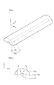
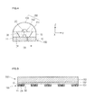
- FIG. 1 is a perspective view showing a light emitting module according to a first embodiment
- FIG. 2 is a perspective view showing a lens of FIG. 1 ;
- FIG. 3 is a view showing an example of light exit in the lens of FIG. 1 ;
- FIG. 4 is a sectional view taken along line A-A of FIG. 1 ;
- FIG. 5 is a sectional view taken along line B-B of FIG. 1 ;
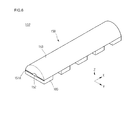
- FIG. 6 is a perspective view showing a light unit according to a second embodiment
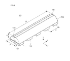
- FIG. 7 is a perspective view showing a light unit according to a third embodiment
- FIG. 8 is a perspective view showing a light unit according to a fourth embodiment
- FIG. 9 is a perspective view showing a light unit according to a fifth embodiment.
- FIG. 10 is a perspective view showing a display apparatus including an another light emitting module of FIG. 9 ;
- FIG. 11 is a perspective view showing a display apparatus including a light emitting module according to the embodiment.
- FIG. 12 is a perspective view showing a display apparatus including a light emitting module according to another embodiment
- FIG. 13 is a side sectional view of FIG. 12 ;
- FIG. 14 is a perspective view showing a display apparatus including the light emitting module according to the embodiment.
- each layer shown in the drawings may be exaggerated, omitted or schematically drawn for the purpose of convenience or clarity.
- the size of elements does not utterly reflect an actual size.
- FIG. 1 is a perspective view showing a light emitting module according to a first embodiment
- FIG. 2 is a perspective view showing a lens of FIG. 1
- FIG. 3 is a view showing an example of light exit in the lens of FIG. 1
- FIG. 4 is a sectional view taken along line A-A of FIG. 1
- FIG. 5 is a sectional view taken along line B-B of FIG. 1 .
- a light emitting module 101 includes a plurality of light emitting devices 100 and a lens 150 having a predetermined length.
- the lens may include a semi-cylinder lens.
- the light emitting devices 100 include at least one of devices emitting red, green, UV (ultraviolet), white lights.
- the lights emitted from the light emitting devices 100 may include a light emitted from a light emitting diode or a light mixed with another color light.
- the light emitting devices 100 are arrayed under the lens 150 in an X axis direction of the lens 150.
- the X axis direction of the lens 150 may be defined as a longitudinal direction of the lens 150.
- the light emitting devices 100 may be arranged at a uniform interval or may be arranged at an irregular interval.
- the lens 120 has a length to cover the light emitting devices 100 above the light emitting devices 100.
- the lens 150 has an outer shape such as a hemispherical shape or a semi-cylinder lens shape.
- the light emitting devices 100 may be disposed on one support member or a plurality of support members.
- the support member may include a substrate or a heat radiation plate, but the embodiment is not limited thereto.
- the light emitting devices 100 are mounted on the substrate and may be connected to each other in series and/or in parallel.
- the light emitting devices 100 include a body 10, lead electrodes 11 and 13, a light emitting diode 20, and a resin member 30.
- the body 10 may include silicon (Si), aluminum (Al), aluminum nitride (AlN), AlO X , PSG (photo sensitive glass), sapphire (Al 2 O 3 ), beryllium oxide (BeO), PCB (Printed Circuit Board), or various resin materials (e.g., PPA), but the embodiment is not limited thereto.
- an insulating layer (not shown) is formed on the surface of the body 10, thereby preventing the body 110 from being shorted with respect to other frames.
- One lead electrode or a plurality of electrodes can be disposed.
- the lead electrodes 11 and 13 may include a metallic material representing electrical conductivity.
- the lead electrodes 11 and 13 may include at least one selected from the group consisting of titanium (Ti), copper (Cu), nickel (Ni), gold (Au), chromium (Cr), tantalum (Ta), platinum (Pt), tin (Sn), silver (Ag), phosphor (P), aluminum (Al), indium (In), palladium (Pd), cobalt (Co), silicon (Si), germanium (Ge), hafnium (Hf), ruthenium (Ru), and iron (Fe), or the alloy thereof.
- the first and second lead electrodes 11 and 13 may have a single layer structure or a multiple layer structure, but the embodiment is not limited thereto.
- the lead electrodes 11 and 13 may be formed through an injection molding process of the body 10. In this case, the lead electrodes 11 and 13 may penetrate through the body 10.
- the cavity 30 may be formed at the upper portion of the body 10, and portions of the lead electrodes 11 and 13 may be disposed in the cavity 30.
- the light emitting diode 20 may be electrically connected to the lead electrodes 11 and 13 in the cavity 10.
- the cavity 30 may be formed independently from the body 10 or may not be formed independently from the body 10.
- the cavity 30 may have a multicavity structure instead of a single-layer cavity structure.
- the lateral surface of the cavity 30 may be inclined, but the embodiment is not limited thereto.
- a resin member is formed on the light emitting diode 20.
- the resin member may be molded in the cavity 30.
- the resin member includes a transmissive resin material such as epoxy or silicon.
- the resin member may include a transmissive material having a low refractive index (e.g., n ⁇ 2.3) to guide a light emitted from the light emitting diode 20 to the outside.
- the surface (i.e., light exit surface) of the resin member may include one of a concave shape, a flat shape, and a convex shape, but the embodiment is not limited thereto.
- a width D3 of the light exit surface of the light emitting device 100 may be equal to or less than a width D1 (see FIG. 1 ) of the lens 150, so that most light emitted from the light exit surface of the light emitting device 100 can be incident into the lens 150 without light loss.
- the length of the light emitting device 100 in a Y axis direction may be less that or greater than the width D1 of the lens 150, but the embodiment is not limited thereto.
- the light emitting devices 100 may be connected to each other in series or several light emitting devices 100 may be connected to each other in parallel, but the embodiment is not limited thereto.
- the lens 150 may have a hemi-cylindrical shape, a semi-spherical shape, or a polygonal shape in which the length D2 of the lens 150 in the X axis direction is longer than the width D1 of the lens 150 in the Y axis direction.
- the X axis direction is perpendicular to the Y axis direction
- a Z axis direction is perpendicular to the X axis direction or the Y axis direction, thereby forming directions to output lights.
- the length D2 of the lens 150 may be two times longer than the width D1 of the lens 150, or may be a length to array several light emitting devices 100.
- the lens 150 may include a plastic material or a glass material.
- the lens 150 may include a resin material or a light transmissive material having a refractive index approximately identical to that of the resin member.
- the lens 150 includes a light incident part 151, a pattern 152 formed at a predetermined region of the light incident part 151 in the X axis direction, and a light exit part 153 to output a light.
- the light incident part 151 of the lens 150 receives a light, and the pattern 152 refracts or diffuses the light.
- the pattern 152 has a cylinder shape, and may be formed in a concaved shape on the flat surface of the light incident part 151.
- the light exit part 153 is disposed in opposition to the light incident part 151 to concentrate the light incident onto the light incident part 151 and the pattern 152.
- the light incident part 151 has an area narrower than that of the light exit part 153.
- the light incident part 151 actually has the shape of a flat surface, and the light exit part 153 has a hemi-spherical shape.
- the light incident part 151 of the lens 150 receives the incident light, and the pattern 152 diffuses the incident light into the lens.
- the light exit part 153 concentrates lights incident through the light incident part 151 and the pattern 152.
- the light incident part 151 has a size small than that of light exit part 153.
- the light incident part 151 is formed of a substantially plane shape and the light exit part 153 is formed of a substantially hemisphere shape.
- the pattern 152 of the lens 150 is disposed substantially perpendicularly to the light emitting diode 10 of the light emitting device 100. Air may be filled in the region PI (see FIG. 4 ) between the pattern 152 and the light exit surface of the light emitting device 100 or another transmissive resin layer may be disposed in the region P1 (see FIG. 4 ) between the pattern 152 and the light exit surface of the light emitting device 100.
- the light incident part 151 of the lens 150 may be attached to the top surface of the light emitting device 100 by using an adhesive agent, and the adhesive agent may include a transmissive adhesive agent such as silicon or epoxy.
- the light transmissive adhesive agent transmits a light output through the light exit surface of the light emitting device 100 to the lens 150 without light loss. In this case, the reflectance on the light exit surface of the light emitting device 100 can be reduced.
- the light incident part 151 of the lens 150 may make contact with the light exit surface of the light emitting device 100 or may not make contact with the light exit surface of the light emitting device 100.
- the interval T between the light emitting devices 100 disposed under the lens 150 is not constant, the lights emitted from the light emitting device 100 are diffused and refracted by the lens 150 and concentrated within a predetermined light irradiation range. Accordingly, the lights emitted from the light emitting device 100 are incident into the lens 150 and concentrated by the lens 150, so that light loss can be reduced.
- the light irradiation range may vary according the diameter or the width of the lens 150.
- the lens 150 can concentrate lights, which are incident at various angles, through the light exit part 153, so that the uniformity in the light intensity and chromaticity can be improved.
- FIG. 6 is a view showing a light emitting module 102 according to the second embodiment.
- the light emitting module 102 includes patterns 152 and 151A having different shapes and formed at a light incident part of the lens 150.
- the patterns 152 and 151A include the first pattern 152 having the shape of a semi-cylinder and the second patterns 151 A having the shape of a polygonal prism at both sides of the first pattern 152.
- the second patterns 151A having the shape of the polygonal prism are arranged in the shape of the concave pattern such as the shape of a chopping wave or a sawtooth wave.
- the second patterns 151A concave patterns and convex patterns are alternately aligned with each other at a uniform interval or an irregular interval.
- the second patterns 151A may be arranged at an interval gradually narrowed or widened in an outward direction
- the lengths of the first pattern 152 and the second patterns 151A may be equal to the length of the lens 150.
- the light incident part of the lens 150 diffuses the light incident into the first pattern 152, and changes the critical angle of the light by the second patterns 151A to reduce a reflected light.
- the lens 150 can concentrate lights incident at various angles through the light exit part 153, so that the uniformity in the light intensity and chromaticity can be improved.
- FIG. 7 is a perspective view showing a light emitting module 103 according to a third embodiment.
- a plurality of devices 20A are arrayed on a substrate 50, and the lens 150 is disposed on the light emitting devices 20A.
- the substrate 50 may include a PCB (Printed Circuit Board) including a circuit pattern (not shown).
- the substrate 50 may include an MCPCB (Metal Core PCB) or an FPCB (Flexible PCB) as well as a typical PCB, but the embodiment is not limited thereto.
- the light emitting devices 20A include a light emitting diode disposed on the substrate 50, or a light emitting diode package as shown in FIG. 4 .
- the light emitting devices 20A are arrayed at a uniform interval or an irregular interval corresponding to the first pattern 152 of the lens 150.
- the lens 150 includes a support part 154, and the support part 154 is disposed at both sides of the lens 150.
- the support part 154 more protrudes downward than the light incident part 151 B protrudes.
- the support part 154 is disposed at both sides of the substrate 50.
- An adhesive member 155 is disposed between the light incident part 151B of the lens 150 and the substrate 50.
- the adhesive member 155 includes a light transmissive adhesive agent or a resin member.
- FIG. 8 is a perspective view showing a light emitting module 104 according to a fourth embodiment.
- the light emitting module 104 includes a lens 150A to cover the light emitting devices 100 above the light emitting devices 100.
- the lens 150A may have the shape of a semi-cylinder.
- a light exit part 153A of the lens 150A may have a many-sided structure, for example, a six-sided structure.
- the light ext part 153A of the lens 150A diffuses a light incident through a light incident part to both sides thereof.
- FIG. 9 is a perspective view showing a light emitting module 105 according to a fifth embodiment.
- the light emitting module 105 includes a lens 150B to cover the light emitting devices 100 above the light emitting devices 100.
- the lens 150B includes a light exit part 153B having a hemi-spherical shape.
- the light exist part 153B is disposed at the central portion thereof with a concave groove 153C formed in the longitudinal direction of the lens 150B, and the concave groove 153C is disposed therein with a reflective member 160.
- the reflective member 160 may diffuse an incident light to both sides or transmit a portion of the light.
- the reflective member 160 may include at least one selected from the group consisting of a metallic material including aluminum (Al) or silver (Ag), a photoresist material, and a metallic oxide such as TiO 2 .
- the reflective member 160 may include a material representing reflectance higher than light transmittance.
- the lens 150B can diffuse the light incident from the light emitting devices 100 to both sides.
- the light emitting module according to the embodiment is applicable to the light unit.
- the light unit is applicable to a display apparatus shown in FIGS. 10 to 13 .
- the light unit is applicable to lighting, a signal lamp, a headlamp of a vehicle, and an electronic display board.
- FIG. 10 is a perspective view showing another light emitting module 105 of FIG. 9 .
- the light emitting module 105 includes a lens 150B to cover the light emitting devices 100 above the light emitting devices 100.
- the light exist part 153B is disposed at the central portion thereof with a concave groove 153C formed in the longitudinal direction of the lens 150B, and the concave groove 153C is disposed therein with a plurality of reflective members 160.
- An interval between the reflective members 160 has a regular interval or an irregular interval.
- the reflective members 160 may include at least one selected from the group consisting of a metallic material including aluminum (Al) or silver (Ag), a photoresist material, and a metallic oxide such as TiO 2
- the reflective members 160 may include a material representing reflectance higher than light transmittance.
- the groove 153C in the light exit part 153B may be formed in plurality.
- FIG. 11 is a view showing a display apparatus 1000 including the light emitting module according to the embodiment.
- the display apparatus 1000 includes a light guide plate 1041, a light emitting module 1031 to supply a light to the light guide plate 1041, a reflective plate 1022 disposed under the light guide plate 1041, an optical sheet 1051 disposed above the light guide plate 1041, a display panel 1051 disposed above the optical sheet 1051, and a bottom cover 1011 to receive the light guide plate 1041, the light emitting module 1031, and the reflective plate 1022, but the embodiment is not limited thereto.
- the bottom cover 1011, the reflective plate 1022, the light emitting module 1033, the light guide plate 1041, and the optical sheet 1051 may be defined as a light unit 1050.
- the light guide plate 1041 diffuses a light to supply a surface light.
- the light guide plate 1041 includes a transparent material.
- the light guide plate 1041 may include one selected from the group consisting of acryl-based resin, such as PMMA (polymethyl methacrylate), PET (polyethylene terephthalate), PC (polycarbonate), COC (cycloolefin copolymer) and PEN (polyethylene naphthalate) resin.
- the bottom surface of the light guide plate 1041 may have a reflective pattern, and the top surface of the light guide plate 1041 may have a flat structure without a pattern or may have a prism pattern.
- the light emitting module 1031 supplies a light into the light incident part of the light guide plate 1041.
- the light emitting module 1031 supplies a light to at least one lateral surface of the light guide plate 1041 to serve as a light source of the display apparatus 1000.
- a plurality of light emitting modules 1031 may be arranged on at least two lateral surfaces of the light guide plate 1041.
- the light emitting module 1031 includes a substrate 1033, a plurality of light emitting devices 100, and a lens 150.
- the light emitting module 1031 includes one structure disclosed in the embodiments.
- the lens 150 may be disposed between the light emitting devices 100 and one lateral surface of the light guide plate 1041.
- the lens 150 may be embedded in the light emitting module 1031 or may be disposed separately from the light emitting module 1031, but the embodiment is not limited thereto.
- the light emitting devices 100 may be mounted on a lateral surface of the bottom cover 1011 or a heat radiation plate instead of the substrate 1033. In this case, the substrate 1033 may be omitted.
- the lens 150 concentrates lights emitted from the light emitting devices 100 into one lateral surface of the light guide plate 1041, thereby reducing the loss of light leaking between the light guide plate 1041 and the light emitting device 100.
- the light incident into the light guide plate 1041 is guided into the light guide plate 1041 and changed into a surface light.
- the lens 150 may have a length corresponding to a length of one lateral surface of the light guide plate 1041.
- the light emitting devices 100 may directly or indirectly supply a light into the light incident part which is one lateral surface of the light guide plate 1041, but the embodiment is not limited thereto.
- the reflective plate 1022 may be disposed under the light guide plate 1041.
- the reflective plate 1022 reflects a light, which is incident from the bottom surface of the light guide plate 1041, upward, so that the brightness of the light unit 1050 can be improved.
- the reflective plate 1022 may include a sheet including a material, such as Al or Ag, representing high reflectance or may include a surface coated on the bottom cover 1011, but the embodiment is not limited thereto.
- the bottom cover 1011 may receive the light guide plate 1041, the light emitting module 1031, and the reflective plate 1022. To this end, the bottom cover 1011 may include a receiving part 1012 having the shape of a box having an open upper portion, but the embodiment is not limited thereto. The bottom cover 1011 may be coupled with a top cover, but the embodiment is not limited thereto.
- the bottom cover 1011 may include a metallic material or a resin material, and may be manufactured through a press molding process or an extrusion molding process.
- the bottom cover 1011 may include a metallic material or a non-metallic material representing superior thermal conductivity, but the embodiment is not limited thereto.
- the optical sheet 1051 is disposed between the display panel 1061 and the light guide plate 1041 and includes at least one transmissive sheet.
- the optical sheet 1051 includes at least one of a diffusion sheet, a horizontal and vertical prism sheet, a luminescence sheet, and a brightness enhancement sheet.
- the diffusion sheet diffuses the incident light
- the horizontal and vertical prism sheet concentrates the incident light onto the display region
- the brightness enhancement sheet improves the brightness by reusing the lost light.
- a protective sheet can be disposed on the display panel 1061, but the embodiment is not limited thereto.
- the luminescence sheet includes luminescence materials representing one color or various colors.
- the luminescence sheet may have a single layer structure or a multi-layer structure including homogeneous luminescence materials or heterogeneous luminescence materials.
- the display panel 1061 for instance, is an LCD panel including first and second transparent substrates, which are opposite to each other, and a liquid crystal layer interposed between the first and second substrates.
- a polarizing plate can be attached to at least one surface of the display panel 1061, but the embodiment is not limited thereto.
- the display panel 1061 displays information by a light passing through the optical sheet 1051.
- the display device 1000 is applicable to various portable terminals, monitors or laptop computers, and televisions.
- the light guide plate 1041 and the optical sheet 1051 can be disposed in the light path of the light emitting module 1031 as optical members, but the embodiment is not limited thereto.
- FIG. 12 is a perspective view showing a display apparatus 100A including a light emitting module according to the embodiment
- FIG. 13 is a side sectional view showing the assembly of FIG. 12 .
- the display apparatus 1000A includes the bottom cover 1011, a reflective plate 1020, the light emitting module 1031, the light guide plate 1041, the optical sheet 1051, and the display panel 1061.
- the light emitting module 1031 generates a light and concentrates the light.
- the light guide plate 1041 changes the light incident from the light emitting module 1031 into a surface light and supplies the surface light to the display panel 1061.
- the bottom surface of the light guide plate 1041 may have a reflective pattern, and the top surface of the light guide plate 1041 may have a flat structure without a pattern or may have a prism pattern.
- the light emitting module 1031 may be coupled with a portion of the reflective plate 1020 on one internal lateral surface of the bottom cover 1011.
- the reflective plate 1020 includes a bottom part 1023, a side part 1024, and a top part 1025.
- the bottom part 1023 is disposed on a bottom surface of the bottom cover 1011 to reflect a light directed downward through the light guide plate 1041 and the light emitting device 100.
- the side part 1024 is bent from one end of the bottom part 1023 in a vertical direction, and an opening 1026 is defined by the side part 1024 and the bottom part 1023.
- the opening 1026 may be formed in the array direction (i.e., X axis direction) of the light emitting devices 100.
- the light emitting devices 100 and the lens 150 may be inserted into the opening 1026.
- the side part 1024 of the reflective member 1020 may be attached to the substrate 1033, but the embodiment is not limited thereto.
- the top part 1025 is bent inward from the side part 1024 so that the top part 1025 is disposed in opposition to one surface of the bottom part 1023.
- the height of the side part 1024 of the reflective plate 1020 may approximately equal to the thickness of the light guide plate 1041 or may be greater than the thickness of the light guide plate 1041.
- the top part 1025 of the reflective plate 1020 may overlap with an edge of a top surface of the light guide plate 1041.
- the top part 1025 and the bottom part 1023 of the reflective plate 1020 are disposed at the top and bottom between the light emitting device 100 and the light guide plate 1041 to reflect a leaking light among lights irradiated from the lens 150. Accordingly, the loss of the light emitted from the light emitting device 100 can be reduced, so that the overall brightness can be improved.
- the top part 1025 of the reflective plate 1020 blocks a light leaking upward between the light guide plate 1041 and the substrate 1033 to prevent light leakage. Accordingly, the light leakage can be prevented, so that the reliability for the light unit 1050 can be improved.
- FIG. 14 is a view showing a display apparatus 1100 including a light emitting module according to the embodiment.
- the display apparatus 1100 includes a bottom cover 1152, a plurality of light emitting modules 1060 disclosed in the embodiments, an optical member 1154, and a display panel 1155.
- the light emitting module 1060 includes the substrate 1120, the light emitting device 100, and the lens 150.
- the light unit 1050 may include the bottom cover 1152, the light emitting modules 1060, and the optical member 1154.
- the bottom cover 1152 may include a receiving part 1153, but the embodiment is not limited thereto.
- the light emitting module 1060 includes the light emitting devices 100 disposed on the substrate 1120, and the lens 150 may be disposed on the light emitting devices 100 as shown in FIG. 1 .
- the lens 150 can concentrate a light emitted from the light emitting device 100. Accordingly, the intensity of the light can be improved by the lens 150 performing a light concentrating function.
- the lenses 150 may be arranged at an interval T2 to prevent a dark part on the display panel 1155.
- the lens 150 may be spaced apart from the optical member 1155, but the embodiment is not limited thereto.
- the optical member 1154 may include at least one of a light guide plate, a diffusion sheet, horizontal and vertical prism sheets, and a brightness enhancement sheet.
- the light guide plate may include a PC material or a PMMA (Poly methyl methacrylate) material.
- the light guide plate may be omitted.
- the diffusion sheet diffuses an incident light
- the horizontal and vertical prism sheets concentrate the incident light into the display region
- the brightness enhancement sheet reuses lost light to improve the brightness.
- a dispersing agent may be contained into the lens 150 or the stack structure of the light guide plate and the optical sheet may be disposed. Accordingly, although the interval T2 of the lenses 150 is increased, the light uniformity can be improved.
- the light emitting modules according to the embodiments are applicable to a lighting system such as a lamp, an indicator, and an electrical sign board as well as the display apparatus, but the embodiment is not limited thereto.
- any reference in this specification to "one embodiment,” “an embodiment,” “example embodiment,” etc. means that a particular feature, structure, or characteristic described in connection with the embodiment is included in at least one embodiment of the invention.
- the appearances of such phrases in various places in the specification are not necessarily all referring to the same embodiment.
Landscapes
- Physics & Mathematics (AREA)
- General Physics & Mathematics (AREA)
- Optics & Photonics (AREA)
- Planar Illumination Modules (AREA)
- Led Device Packages (AREA)
- Illuminated Signs And Luminous Advertising (AREA)
Abstract
Description
- The embodiment relates to a light unit and a display apparatus having the same.
- A light emitting diode (LED) is a semiconductor light emitting device that converts current into light. The LED can generate light having high brightness, so that the LED has been expensively used as a light source for a display device, a vehicle, or a lighting device. In addition, the LED can represent a white color having superior light efficiency by luminescence materials or combining LEDs having various colors.
- The embodiment provides a light unit including a semi-cylinder lens disposed on a plurality of light emitting devices and a display apparatus having the same.
- The embodiment provides a light unit including a semi-cylinder lens having a pattern formed at a part receiving lights emitted from a plurality of light emitting devices and a display apparatus having the same.
- According to the embodiment, the light unit includes a lens including a light incident part having a first pattern and a light exit part, a plurality of light emitting devices arrayed under the incident part of the lens, and a substrate having the light emitting devices mounted thereon, wherein the light incident part of the lens includes a flat surface and the lens has a length different from a width of lens, and the first pattern of the light incident part of the lens is disposed at a central portion of the light incident part and is formed in the length of the lens and having a concave shape.
- According to the embodiment, the light unit includes a substrate, a plurality of light emitting diodes disposed in a first direction on the substrate, a lens on the light emitting diodes, and a adhesive member between the substrate and the lens. The lens includes a light incident part having a first pattern in the first direction, and a light exit part to emit a light incident through the light incident part, wherein the light incident part of the lens includes a flat surface and the lens has a length different from a width of lens, and the first pattern of the light incident part of the lens is disposed at a central portion of the light incident part and is formed in the length of the lens and having a concave shape.
- According to the embodiment, a display apparatus includes a plurality of light emitting devices, a substrate having the light emitting devices arrayed in a first direction, a lens on the light emitting devices, an optical member including at least one of a light guide plate and the optical sheet at one side of the lens, and a display panel on the optical member. The lens includes a light incident part on the light emitting device, a pattern having a cylinder shape and disposed in the first direction of the light incident part, and a light exit part to output a light incident through the light incident part.
-
FIG. 1 is a perspective view showing a light emitting module according to a first embodiment; -
FIG. 2 is a perspective view showing a lens ofFIG. 1 ; -
FIG. 3 is a view showing an example of light exit in the lens ofFIG. 1 ; -
FIG. 4 is a sectional view taken along line A-A ofFIG. 1 ; -
FIG. 5 is a sectional view taken along line B-B ofFIG. 1 ; -
FIG. 6 is a perspective view showing a light unit according to a second embodiment; -
FIG. 7 is a perspective view showing a light unit according to a third embodiment; -
FIG. 8 is a perspective view showing a light unit according to a fourth embodiment; -
FIG. 9 is a perspective view showing a light unit according to a fifth embodiment; -
FIG. 10 is a perspective view showing a display apparatus including an another light emitting module ofFIG. 9 ; -
FIG. 11 is a perspective view showing a display apparatus including a light emitting module according to the embodiment; -
FIG. 12 is a perspective view showing a display apparatus including a light emitting module according to another embodiment; -
FIG. 13 is a side sectional view ofFIG. 12 ; and -
FIG. 14 is a perspective view showing a display apparatus including the light emitting module according to the embodiment. - In the description of the embodiments, it will be understood that, when a layer (or film), a region, a pattern, or a structure is referred to as being "on" or "under" another substrate, another layer (or film), another region, another pad, or another pattern, it can be "directly" or "indirectly" over the other substrate, layer (or film), region, pad, or pattern, or one or more intervening layers may also be present. Such a position of the layer has been described with reference to the drawings.
- The thickness and size of each layer shown in the drawings may be exaggerated, omitted or schematically drawn for the purpose of convenience or clarity. In addition, the size of elements does not utterly reflect an actual size.
-
FIG. 1 is a perspective view showing a light emitting module according to a first embodiment, andFIG. 2 is a perspective view showing a lens ofFIG. 1 .FIG. 3 is a view showing an example of light exit in the lens ofFIG. 1 , andFIG. 4 is a sectional view taken along line A-A ofFIG. 1 .FIG. 5 is a sectional view taken along line B-B ofFIG. 1 . - Referring to
FIGS. 1 to 5 , alight emitting module 101 includes a plurality oflight emitting devices 100 and alens 150 having a predetermined length. The lens may include a semi-cylinder lens. - The
light emitting devices 100 include at least one of devices emitting red, green, UV (ultraviolet), white lights. The lights emitted from thelight emitting devices 100 may include a light emitted from a light emitting diode or a light mixed with another color light. - The
light emitting devices 100 are arrayed under thelens 150 in an X axis direction of thelens 150. The X axis direction of thelens 150 may be defined as a longitudinal direction of thelens 150. - The
light emitting devices 100 may be arranged at a uniform interval or may be arranged at an irregular interval. The lens 120 has a length to cover thelight emitting devices 100 above thelight emitting devices 100. Thelens 150 has an outer shape such as a hemispherical shape or a semi-cylinder lens shape. - The
light emitting devices 100 may be disposed on one support member or a plurality of support members. The support member may include a substrate or a heat radiation plate, but the embodiment is not limited thereto. Thelight emitting devices 100 are mounted on the substrate and may be connected to each other in series and/or in parallel. - Referring to
FIGS. 4 and 5 , thelight emitting devices 100 include abody 10,lead electrodes 11 and 13, alight emitting diode 20, and aresin member 30. Thebody 10 may include silicon (Si), aluminum (Al), aluminum nitride (AlN), AlOX, PSG (photo sensitive glass), sapphire (Al2O3), beryllium oxide (BeO), PCB (Printed Circuit Board), or various resin materials (e.g., PPA), but the embodiment is not limited thereto. - If the
body 10 includes an electrical conductivity material, an insulating layer (not shown) is formed on the surface of thebody 10, thereby preventing the body 110 from being shorted with respect to other frames. One lead electrode or a plurality of electrodes can be disposed. Thelead electrodes 11 and 13 may include a metallic material representing electrical conductivity. For example, thelead electrodes 11 and 13 may include at least one selected from the group consisting of titanium (Ti), copper (Cu), nickel (Ni), gold (Au), chromium (Cr), tantalum (Ta), platinum (Pt), tin (Sn), silver (Ag), phosphor (P), aluminum (Al), indium (In), palladium (Pd), cobalt (Co), silicon (Si), germanium (Ge), hafnium (Hf), ruthenium (Ru), and iron (Fe), or the alloy thereof. The first andsecond lead electrodes 11 and 13 may have a single layer structure or a multiple layer structure, but the embodiment is not limited thereto. Thelead electrodes 11 and 13 may be formed through an injection molding process of thebody 10. In this case, thelead electrodes 11 and 13 may penetrate through thebody 10. - The
cavity 30 may be formed at the upper portion of thebody 10, and portions of thelead electrodes 11 and 13 may be disposed in thecavity 30. Thelight emitting diode 20 may be electrically connected to thelead electrodes 11 and 13 in thecavity 10. Thecavity 30 may be formed independently from thebody 10 or may not be formed independently from thebody 10. In addition, thecavity 30 may have a multicavity structure instead of a single-layer cavity structure. The lateral surface of thecavity 30 may be inclined, but the embodiment is not limited thereto. - A resin member is formed on the
light emitting diode 20. When thelight emitting diode 20 is disposed in thecavity 30, the resin member may be molded in thecavity 30. The resin member includes a transmissive resin material such as epoxy or silicon. The resin member may include a transmissive material having a low refractive index (e.g., n<2.3) to guide a light emitted from thelight emitting diode 20 to the outside. The surface (i.e., light exit surface) of the resin member may include one of a concave shape, a flat shape, and a convex shape, but the embodiment is not limited thereto. - A width D3 of the light exit surface of the
light emitting device 100 may be equal to or less than a width D1 (seeFIG. 1 ) of thelens 150, so that most light emitted from the light exit surface of thelight emitting device 100 can be incident into thelens 150 without light loss. The length of thelight emitting device 100 in a Y axis direction may be less that or greater than the width D1 of thelens 150, but the embodiment is not limited thereto. - The
light emitting devices 100 may be connected to each other in series or several light emittingdevices 100 may be connected to each other in parallel, but the embodiment is not limited thereto. - As shown in
FIGS. 1 to 4 , thelens 150 may have a hemi-cylindrical shape, a semi-spherical shape, or a polygonal shape in which the length D2 of thelens 150 in the X axis direction is longer than the width D1 of thelens 150 in the Y axis direction. The X axis direction is perpendicular to the Y axis direction, and a Z axis direction is perpendicular to the X axis direction or the Y axis direction, thereby forming directions to output lights. The length D2 of thelens 150 may be two times longer than the width D1 of thelens 150, or may be a length to array several light emittingdevices 100. - The
lens 150 may include a plastic material or a glass material. In addition, thelens 150 may include a resin material or a light transmissive material having a refractive index approximately identical to that of the resin member. - Referring to
FIGS. 2 and 3 , thelens 150 includes alight incident part 151, apattern 152 formed at a predetermined region of thelight incident part 151 in the X axis direction, and alight exit part 153 to output a light. - The
light incident part 151 of thelens 150 receives a light, and thepattern 152 refracts or diffuses the light. Thepattern 152 has a cylinder shape, and may be formed in a concaved shape on the flat surface of thelight incident part 151. Thelight exit part 153 is disposed in opposition to thelight incident part 151 to concentrate the light incident onto thelight incident part 151 and thepattern 152. Thelight incident part 151 has an area narrower than that of thelight exit part 153. For example, thelight incident part 151 actually has the shape of a flat surface, and thelight exit part 153 has a hemi-spherical shape. - The
light incident part 151 of thelens 150 receives the incident light, and thepattern 152 diffuses the incident light into the lens. Thelight exit part 153 concentrates lights incident through thelight incident part 151 and thepattern 152. Thelight incident part 151 has a size small than that oflight exit part 153. Thelight incident part 151 is formed of a substantially plane shape and thelight exit part 153 is formed of a substantially hemisphere shape. - Referring to
FIGS. 1 and4 , thepattern 152 of thelens 150 is disposed substantially perpendicularly to thelight emitting diode 10 of thelight emitting device 100. Air may be filled in the region PI (seeFIG. 4 ) between thepattern 152 and the light exit surface of thelight emitting device 100 or another transmissive resin layer may be disposed in the region P1 (seeFIG. 4 ) between thepattern 152 and the light exit surface of thelight emitting device 100. - The
light incident part 151 of thelens 150 may be attached to the top surface of thelight emitting device 100 by using an adhesive agent, and the adhesive agent may include a transmissive adhesive agent such as silicon or epoxy. The light transmissive adhesive agent transmits a light output through the light exit surface of thelight emitting device 100 to thelens 150 without light loss. In this case, the reflectance on the light exit surface of thelight emitting device 100 can be reduced. Thelight incident part 151 of thelens 150 may make contact with the light exit surface of thelight emitting device 100 or may not make contact with the light exit surface of thelight emitting device 100. - In this case, although the interval T between the light emitting
devices 100 disposed under thelens 150 is not constant, the lights emitted from thelight emitting device 100 are diffused and refracted by thelens 150 and concentrated within a predetermined light irradiation range. Accordingly, the lights emitted from thelight emitting device 100 are incident into thelens 150 and concentrated by thelens 150, so that light loss can be reduced. The light irradiation range may vary according the diameter or the width of thelens 150. - The
lens 150 can concentrate lights, which are incident at various angles, through thelight exit part 153, so that the uniformity in the light intensity and chromaticity can be improved. -
FIG. 6 is a view showing alight emitting module 102 according to the second embodiment. - Referring to
FIG. 5 , thelight emitting module 102 includespatterns lens 150. Thepatterns first pattern 152 having the shape of a semi-cylinder and thesecond patterns 151 A having the shape of a polygonal prism at both sides of thefirst pattern 152. Thesecond patterns 151A having the shape of the polygonal prism are arranged in the shape of the concave pattern such as the shape of a chopping wave or a sawtooth wave. - In the
second patterns 151A, concave patterns and convex patterns are alternately aligned with each other at a uniform interval or an irregular interval. In addition, thesecond patterns 151A may be arranged at an interval gradually narrowed or widened in an outward direction - The lengths of the
first pattern 152 and thesecond patterns 151A may be equal to the length of thelens 150. - The light incident part of the
lens 150 diffuses the light incident into thefirst pattern 152, and changes the critical angle of the light by thesecond patterns 151A to reduce a reflected light. - Accordingly, since the
lens 150 can concentrate lights incident at various angles through thelight exit part 153, so that the uniformity in the light intensity and chromaticity can be improved. -
FIG. 7 is a perspective view showing alight emitting module 103 according to a third embodiment. - Referring to
FIG. 7 , in thelight emitting module 103, a plurality ofdevices 20A are arrayed on asubstrate 50, and thelens 150 is disposed on thelight emitting devices 20A. - The
substrate 50 may include a PCB (Printed Circuit Board) including a circuit pattern (not shown). Thesubstrate 50 may include an MCPCB (Metal Core PCB) or an FPCB (Flexible PCB) as well as a typical PCB, but the embodiment is not limited thereto. - The
light emitting devices 20A include a light emitting diode disposed on thesubstrate 50, or a light emitting diode package as shown inFIG. 4 . Thelight emitting devices 20A are arrayed at a uniform interval or an irregular interval corresponding to thefirst pattern 152 of thelens 150. - The
lens 150 includes asupport part 154, and thesupport part 154 is disposed at both sides of thelens 150. Thesupport part 154 more protrudes downward than thelight incident part 151 B protrudes. Thesupport part 154 is disposed at both sides of thesubstrate 50. - An
adhesive member 155 is disposed between thelight incident part 151B of thelens 150 and thesubstrate 50. Theadhesive member 155 includes a light transmissive adhesive agent or a resin member. -
FIG. 8 is a perspective view showing alight emitting module 104 according to a fourth embodiment. - Referring to
FIG. 8 , thelight emitting module 104 includes alens 150A to cover thelight emitting devices 100 above thelight emitting devices 100. - The
lens 150A may have the shape of a semi-cylinder. Alight exit part 153A of thelens 150A may have a many-sided structure, for example, a six-sided structure. The light extpart 153A of thelens 150A diffuses a light incident through a light incident part to both sides thereof. -
FIG. 9 is a perspective view showing alight emitting module 105 according to a fifth embodiment. - Referring to
FIG. 9 , thelight emitting module 105 includes alens 150B to cover thelight emitting devices 100 above thelight emitting devices 100. Thelens 150B includes a light exit part 153B having a hemi-spherical shape. The light exist part 153B is disposed at the central portion thereof with aconcave groove 153C formed in the longitudinal direction of thelens 150B, and theconcave groove 153C is disposed therein with areflective member 160. Thereflective member 160 may diffuse an incident light to both sides or transmit a portion of the light. Thereflective member 160 may include at least one selected from the group consisting of a metallic material including aluminum (Al) or silver (Ag), a photoresist material, and a metallic oxide such as TiO2. Thereflective member 160 may include a material representing reflectance higher than light transmittance. Thelens 150B can diffuse the light incident from thelight emitting devices 100 to both sides. - The light emitting module according to the embodiment is applicable to the light unit. The light unit is applicable to a display apparatus shown in
FIGS. 10 to 13 . In addition the light unit is applicable to lighting, a signal lamp, a headlamp of a vehicle, and an electronic display board. -
FIG. 10 is a perspective view showing anotherlight emitting module 105 ofFIG. 9 . - Referring to
FIG. 10 , thelight emitting module 105 includes alens 150B to cover thelight emitting devices 100 above thelight emitting devices 100. The light exist part 153B is disposed at the central portion thereof with aconcave groove 153C formed in the longitudinal direction of thelens 150B, and theconcave groove 153C is disposed therein with a plurality ofreflective members 160. An interval between thereflective members 160 has a regular interval or an irregular interval. Thereflective members 160 may include at least one selected from the group consisting of a metallic material including aluminum (Al) or silver (Ag), a photoresist material, and a metallic oxide such as TiO2 Thereflective members 160 may include a material representing reflectance higher than light transmittance. Thegroove 153C in the light exit part 153B may be formed in plurality. -
FIG. 11 is a view showing adisplay apparatus 1000 including the light emitting module according to the embodiment. - Referring to
FIG. 11 , thedisplay apparatus 1000 includes alight guide plate 1041, alight emitting module 1031 to supply a light to thelight guide plate 1041, areflective plate 1022 disposed under thelight guide plate 1041, anoptical sheet 1051 disposed above thelight guide plate 1041, adisplay panel 1051 disposed above theoptical sheet 1051, and abottom cover 1011 to receive thelight guide plate 1041, thelight emitting module 1031, and thereflective plate 1022, but the embodiment is not limited thereto. - The
bottom cover 1011, thereflective plate 1022, thelight emitting module 1033, thelight guide plate 1041, and theoptical sheet 1051 may be defined as alight unit 1050. - The
light guide plate 1041 diffuses a light to supply a surface light. Thelight guide plate 1041 includes a transparent material. For example, thelight guide plate 1041 may include one selected from the group consisting of acryl-based resin, such as PMMA (polymethyl methacrylate), PET (polyethylene terephthalate), PC (polycarbonate), COC (cycloolefin copolymer) and PEN (polyethylene naphthalate) resin. The bottom surface of thelight guide plate 1041 may have a reflective pattern, and the top surface of thelight guide plate 1041 may have a flat structure without a pattern or may have a prism pattern. - The
light emitting module 1031 supplies a light into the light incident part of thelight guide plate 1041. Thelight emitting module 1031 supplies a light to at least one lateral surface of thelight guide plate 1041 to serve as a light source of thedisplay apparatus 1000. A plurality oflight emitting modules 1031 may be arranged on at least two lateral surfaces of thelight guide plate 1041. - The
light emitting module 1031 includes asubstrate 1033, a plurality of light emittingdevices 100, and alens 150. Thelight emitting module 1031 includes one structure disclosed in the embodiments. Thelens 150 may be disposed between the light emittingdevices 100 and one lateral surface of thelight guide plate 1041. Thelens 150 may be embedded in thelight emitting module 1031 or may be disposed separately from thelight emitting module 1031, but the embodiment is not limited thereto. - The
light emitting devices 100 may be mounted on a lateral surface of thebottom cover 1011 or a heat radiation plate instead of thesubstrate 1033. In this case, thesubstrate 1033 may be omitted. - The
lens 150 concentrates lights emitted from thelight emitting devices 100 into one lateral surface of thelight guide plate 1041, thereby reducing the loss of light leaking between thelight guide plate 1041 and thelight emitting device 100. The light incident into thelight guide plate 1041 is guided into thelight guide plate 1041 and changed into a surface light. - The
lens 150 may have a length corresponding to a length of one lateral surface of thelight guide plate 1041. - The
light emitting devices 100 may directly or indirectly supply a light into the light incident part which is one lateral surface of thelight guide plate 1041, but the embodiment is not limited thereto. - The
reflective plate 1022 may be disposed under thelight guide plate 1041. Thereflective plate 1022 reflects a light, which is incident from the bottom surface of thelight guide plate 1041, upward, so that the brightness of thelight unit 1050 can be improved. Thereflective plate 1022 may include a sheet including a material, such as Al or Ag, representing high reflectance or may include a surface coated on thebottom cover 1011, but the embodiment is not limited thereto. - The
bottom cover 1011 may receive thelight guide plate 1041, thelight emitting module 1031, and thereflective plate 1022. To this end, thebottom cover 1011 may include a receivingpart 1012 having the shape of a box having an open upper portion, but the embodiment is not limited thereto. Thebottom cover 1011 may be coupled with a top cover, but the embodiment is not limited thereto. - The
bottom cover 1011 may include a metallic material or a resin material, and may be manufactured through a press molding process or an extrusion molding process. Thebottom cover 1011 may include a metallic material or a non-metallic material representing superior thermal conductivity, but the embodiment is not limited thereto. - The
optical sheet 1051 is disposed between thedisplay panel 1061 and thelight guide plate 1041 and includes at least one transmissive sheet. For instance, theoptical sheet 1051 includes at least one of a diffusion sheet, a horizontal and vertical prism sheet, a luminescence sheet, and a brightness enhancement sheet. The diffusion sheet diffuses the incident light, the horizontal and vertical prism sheet concentrates the incident light onto the display region, and the brightness enhancement sheet improves the brightness by reusing the lost light. In addition, a protective sheet can be disposed on thedisplay panel 1061, but the embodiment is not limited thereto. The luminescence sheet includes luminescence materials representing one color or various colors. In addition, the luminescence sheet may have a single layer structure or a multi-layer structure including homogeneous luminescence materials or heterogeneous luminescence materials. - The
display panel 1061, for instance, is an LCD panel including first and second transparent substrates, which are opposite to each other, and a liquid crystal layer interposed between the first and second substrates. A polarizing plate can be attached to at least one surface of thedisplay panel 1061, but the embodiment is not limited thereto. Thedisplay panel 1061 displays information by a light passing through theoptical sheet 1051. Thedisplay device 1000 is applicable to various portable terminals, monitors or laptop computers, and televisions. - The
light guide plate 1041 and theoptical sheet 1051 can be disposed in the light path of thelight emitting module 1031 as optical members, but the embodiment is not limited thereto. -
FIG. 12 is a perspective view showing a display apparatus 100A including a light emitting module according to the embodiment, andFIG. 13 is a side sectional view showing the assembly ofFIG. 12 . - Referring to
FIGS. 12 and 13 , thedisplay apparatus 1000A includes thebottom cover 1011, areflective plate 1020, thelight emitting module 1031, thelight guide plate 1041, theoptical sheet 1051, and thedisplay panel 1061. - The
light emitting module 1031 generates a light and concentrates the light. Thelight guide plate 1041 changes the light incident from thelight emitting module 1031 into a surface light and supplies the surface light to thedisplay panel 1061. The bottom surface of thelight guide plate 1041 may have a reflective pattern, and the top surface of thelight guide plate 1041 may have a flat structure without a pattern or may have a prism pattern. - The
light emitting module 1031 may be coupled with a portion of thereflective plate 1020 on one internal lateral surface of thebottom cover 1011. - The
reflective plate 1020 includes abottom part 1023, aside part 1024, and atop part 1025. Thebottom part 1023 is disposed on a bottom surface of thebottom cover 1011 to reflect a light directed downward through thelight guide plate 1041 and thelight emitting device 100. Theside part 1024 is bent from one end of thebottom part 1023 in a vertical direction, and anopening 1026 is defined by theside part 1024 and thebottom part 1023. Theopening 1026 may be formed in the array direction (i.e., X axis direction) of thelight emitting devices 100. Thelight emitting devices 100 and thelens 150 may be inserted into theopening 1026. - The
side part 1024 of thereflective member 1020 may be attached to thesubstrate 1033, but the embodiment is not limited thereto. Thetop part 1025 is bent inward from theside part 1024 so that thetop part 1025 is disposed in opposition to one surface of thebottom part 1023. - In this case, the height of the
side part 1024 of thereflective plate 1020 may approximately equal to the thickness of thelight guide plate 1041 or may be greater than the thickness of thelight guide plate 1041. Thetop part 1025 of thereflective plate 1020 may overlap with an edge of a top surface of thelight guide plate 1041. - The
top part 1025 and thebottom part 1023 of thereflective plate 1020 are disposed at the top and bottom between the light emittingdevice 100 and thelight guide plate 1041 to reflect a leaking light among lights irradiated from thelens 150. Accordingly, the loss of the light emitted from thelight emitting device 100 can be reduced, so that the overall brightness can be improved. - The
top part 1025 of thereflective plate 1020 blocks a light leaking upward between thelight guide plate 1041 and thesubstrate 1033 to prevent light leakage. Accordingly, the light leakage can be prevented, so that the reliability for thelight unit 1050 can be improved. -
FIG. 14 is a view showing adisplay apparatus 1100 including a light emitting module according to the embodiment. - Referring to
FIG. 14 , thedisplay apparatus 1100 includes abottom cover 1152, a plurality of light emitting modules 1060 disclosed in the embodiments, anoptical member 1154, and adisplay panel 1155. - The light emitting module 1060 includes the
substrate 1120, thelight emitting device 100, and thelens 150. Thelight unit 1050 may include thebottom cover 1152, the light emitting modules 1060, and theoptical member 1154. - The
bottom cover 1152 may include a receivingpart 1153, but the embodiment is not limited thereto. - The light emitting module 1060 includes the
light emitting devices 100 disposed on thesubstrate 1120, and thelens 150 may be disposed on thelight emitting devices 100 as shown inFIG. 1 . Thelens 150 can concentrate a light emitted from thelight emitting device 100. Accordingly, the intensity of the light can be improved by thelens 150 performing a light concentrating function. Thelenses 150 may be arranged at an interval T2 to prevent a dark part on thedisplay panel 1155. - The
lens 150 may be spaced apart from theoptical member 1155, but the embodiment is not limited thereto. - The
optical member 1154 may include at least one of a light guide plate, a diffusion sheet, horizontal and vertical prism sheets, and a brightness enhancement sheet. The light guide plate may include a PC material or a PMMA (Poly methyl methacrylate) material. The light guide plate may be omitted. The diffusion sheet diffuses an incident light, the horizontal and vertical prism sheets concentrate the incident light into the display region, and the brightness enhancement sheet reuses lost light to improve the brightness. - In order to adjust the interval T2 between the
lenses 150, a dispersing agent may be contained into thelens 150 or the stack structure of the light guide plate and the optical sheet may be disposed. Accordingly, although the interval T2 of thelenses 150 is increased, the light uniformity can be improved. - The light emitting modules according to the embodiments are applicable to a lighting system such as a lamp, an indicator, and an electrical sign board as well as the display apparatus, but the embodiment is not limited thereto.
- Any reference in this specification to "one embodiment," "an embodiment," "example embodiment," etc., means that a particular feature, structure, or characteristic described in connection with the embodiment is included in at least one embodiment of the invention. The appearances of such phrases in various places in the specification are not necessarily all referring to the same embodiment. Further, when a particular feature, structure, or characteristic is described in connection with any embodiment, it is submitted that it is within the purview of one skilled in the art to effect such feature, structure, or characteristic in connection with other ones of the embodiments.
- Although embodiments have been described with reference to a number of illustrative embodiments thereof, it should be understood that numerous other modifications and embodiments can be devised by those skilled in the art that will fall within the spirit and scope of the principles of this disclosure. More particularly, various variations and modifications are possible in the component parts and/or arrangements of the subject combination arrangement within the scope of the disclosure, the drawings and the appended claims. In addition to variations and modifications in the component parts and/or arrangements, alternative uses will also be apparent to those skilled in the art.
Claims (15)
- A light unit comprising:a lens including a light incident part having a first pattern and a light exit part;a plurality of light emitting devices arrayed under the incident part of the lens; anda substrate having the light emitting devices mounted thereon,wherein the light incident part of the lens includes a flat surface and the lens has a length different from a width of lens,wherein the first pattern of the light incident part of the lens is disposed at a central portion of the light incident part and is formed in the length of the lens and having a concave shape.
- The light unit of claim 1, wherein the light exit part of the lens has a semi-cylindrical shape or a multi-sided structure.
- The light unit of claim 1 or 2, wherein the light incident part of the lens includes a second pattern and the second pattern is formed in a concave pattern and a convex pattern which are alternately aligned with each other on a surface of the light incident part of the lens.
- The light unit of claims 1 or 2, wherein the lens includes a semi-cylinder lens and the light incident part of the lens includes a second pattern having a prism shape disposed at both sides of a central portion of the first pattern.
- The light unit of claim 4, wherein the light exit part of the lens is disposed at a central portion thereof with a groove formed in the length direction of the lens and concaved from disposed a surface of the light exit part.
- The light unit of claim 5, the groove of the light exit part is formed in plurality.
- The light unit of claim 5, further comprising a reflective member disposed in the groove of the light exit part.
- The light unit of claim 7, wherein the reflective member includes at least one selected from the group consisting of a metallic material, a photoresist material, and a metallic oxide.
- A light unit comprising:a substrate;a plurality of light emitting diodes disposed in a first direction on the substrate;a lens on the light emitting diodes; andan adhesive member between the substrate and the lens,wherein the lens includes a light incident part having a first pattern in the first direction, and a light exit part to emit a light incident through the light incident part,wherein the light incident part of the lens includes a flat surface and the lens has a length different from a width of lens,wherein the first pattern of the light incident part of the lens is disposed at a central portion of the light incident part and is formed in the length of the lens and having a concave shape.
- The light unit of claim 9, wherein both sides of the light incident part of the lens make contact with the substrate.
- The light unit of claim 9, further comprising an optical member disposed at one side of the lens.
- The light unit of claim 9, wherein the adhesive member includes a resin member.
- A display apparatus comprising:a plurality of light emitting devices;a substrate having the light emitting devices arrayed in a first direction;a lens on the light emitting devices;an optical member including at least one of a light guide plate and the optical sheet at one side of the lens; anda display panel on the optical member,wherein the lens includes:a light incident part on the light emitting device; anda pattern having a cylinder shape and disposed in the first direction of the light incident part, and a light exit part to output a light incident through the light incident part.
- The display apparatus of claim 13, further comprising:a reflective plate disposed under the optical member; anda bottom cover disposed under the reflective plate to cover a peripheral portion of the optical member.
- The display apparatus of claim 14, wherein the reflective plate is disposed at one side thereof with a side part to define an opening into which the light emitting device is inserted.
Applications Claiming Priority (1)
| Application Number | Priority Date | Filing Date | Title |
|---|---|---|---|
| KR1020100030017A KR101064076B1 (en) | 2010-04-01 | 2010-04-01 | Light unit and display device having same |
Publications (3)
| Publication Number | Publication Date |
|---|---|
| EP2378324A2 true EP2378324A2 (en) | 2011-10-19 |
| EP2378324A3 EP2378324A3 (en) | 2012-09-05 |
| EP2378324B1 EP2378324B1 (en) | 2017-12-13 |
Family
ID=44260834
Family Applications (1)
| Application Number | Title | Priority Date | Filing Date |
|---|---|---|---|
| EP11160424.5A Not-in-force EP2378324B1 (en) | 2010-04-01 | 2011-03-30 | Light unit and display apparatus having the same |
Country Status (4)
| Country | Link |
|---|---|
| US (1) | US9645299B2 (en) |
| EP (1) | EP2378324B1 (en) |
| KR (1) | KR101064076B1 (en) |
| CN (1) | CN102252224B (en) |
Families Citing this family (14)
| Publication number | Priority date | Publication date | Assignee | Title |
|---|---|---|---|---|
| KR101962121B1 (en) * | 2011-12-12 | 2019-03-28 | 삼성디스플레이 주식회사 | Lens, backlight module and display apparatus having the lens |
| CN103367616B (en) * | 2012-04-06 | 2018-01-02 | 杭州华普永明光电股份有限公司 | A kind of LED module and its manufacturing process of COB encapsulation |
| CN102889486B (en) * | 2012-10-27 | 2017-04-19 | 欧普照明股份有限公司 | Illumination lamp |
| KR101375224B1 (en) | 2012-12-28 | 2014-03-17 | 주식회사 루멘스 | Method for manufacturing light emitting device package and light emitting device package |
| CN104676463A (en) * | 2013-11-29 | 2015-06-03 | 苏州欧普照明有限公司 | Lens and illuminating apparatus including the lens |
| US10209424B2 (en) | 2014-01-10 | 2019-02-19 | Corning Incorporated | Visual display backlight unit |
| DE102014100582A1 (en) * | 2014-01-20 | 2015-07-23 | Osram Opto Semiconductors Gmbh | Illuminant with predeterminable radiation characteristic and manufacturing method for an optical body |
| KR102264379B1 (en) * | 2014-02-05 | 2021-06-15 | 엘지이노텍 주식회사 | Optical device and lighting device using the same |
| CN105093387B (en) * | 2015-07-31 | 2018-12-07 | 深圳市华星光电技术有限公司 | Light guide plate, backlight module and display device |
| JP6869667B2 (en) * | 2016-08-31 | 2021-05-12 | 三菱電機株式会社 | Surface light source device and liquid crystal display device |
| KR102423202B1 (en) * | 2017-07-18 | 2022-07-20 | 엘지전자 주식회사 | Display device using semiconductor light emitting device |
| TWI668502B (en) * | 2018-04-24 | 2019-08-11 | 微采視像科技股份有限公司 | Light deflection film and display device using the same |
| CN108873149A (en) * | 2018-07-09 | 2018-11-23 | 京东方科技集团股份有限公司 | A kind of light guide plate, backlight module and display device |
| KR102310905B1 (en) * | 2019-06-10 | 2021-10-08 | 유버 주식회사 | Radiation Energy Controller for Ultraviolet Light Emitting Diode |
Family Cites Families (22)
| Publication number | Priority date | Publication date | Assignee | Title |
|---|---|---|---|---|
| US6607286B2 (en) * | 2001-05-04 | 2003-08-19 | Lumileds Lighting, U.S., Llc | Lens and lens cap with sawtooth portion for light emitting diode |
| US6724543B1 (en) * | 2002-10-23 | 2004-04-20 | Visteon Global Technologies, Inc. | Light collection assembly having mixed conic shapes for use with various light emitting sources |
| JP4262113B2 (en) | 2004-02-13 | 2009-05-13 | シチズン電子株式会社 | Backlight |
| KR100576865B1 (en) * | 2004-05-03 | 2006-05-10 | 삼성전기주식회사 | LED array module for backlight and backlight unit having same |
| TW201403859A (en) | 2005-02-18 | 2014-01-16 | 日亞化學工業股份有限公司 | Light-emitting device with lens for controlling light distribution characteristics |
| CN100585268C (en) | 2005-03-07 | 2010-01-27 | 日亚化学工业株式会社 | Planar irradiation light source and planar irradiation device |
| KR101222152B1 (en) * | 2006-02-06 | 2013-01-14 | 삼성디스플레이 주식회사 | Backlight assembly and display device having the same |
| JP2007311588A (en) * | 2006-05-19 | 2007-11-29 | Nichia Chem Ind Ltd | Method for manufacturing light emitting device |
| KR101266490B1 (en) | 2006-09-08 | 2013-05-23 | 삼성디스플레이 주식회사 | Backlight assembly and liquid crystal display having the same |
| CN200952671Y (en) | 2006-09-21 | 2007-09-26 | 一品光学工业股份有限公司 | Improved structure of LED light source device |
| KR20080033000A (en) | 2006-10-12 | 2008-04-16 | 삼성전자주식회사 | Lens for liquid crystal display device, backlight unit and liquid crystal display device having same |
| WO2008062812A1 (en) | 2006-11-21 | 2008-05-29 | Showa Denko K.K. | Light emitting device and surface light emitting device |
| KR20080064262A (en) | 2007-01-04 | 2008-07-09 | 삼성전자주식회사 | Lens for liquid crystal display device, backlight unit and liquid crystal display device having same |
| JP4521013B2 (en) | 2007-05-15 | 2010-08-11 | 株式会社日立製作所 | LIGHTING DEVICE AND LIQUID CRYSTAL DISPLAY DEVICE USING THE LIGHTING DEVICE |
| JP4350144B2 (en) | 2007-08-09 | 2009-10-21 | シャープ株式会社 | LIGHT EMITTING DEVICE AND LIGHTING DEVICE EQUIPPED WITH THE SAME |
| JP4479805B2 (en) * | 2008-02-15 | 2010-06-09 | ソニー株式会社 | Lens, light source unit, backlight device, and display device |
| CN101539266B (en) * | 2008-03-19 | 2011-05-11 | 富准精密工业(深圳)有限公司 | Luminous element and lens thereof |
| KR100939455B1 (en) | 2008-09-01 | 2010-01-29 | 임명춘 | Light emmting diode device |
| KR100974336B1 (en) | 2008-09-12 | 2010-08-05 | 주식회사 루멘스 | Light emitting diode package |
| CN101639181A (en) | 2009-08-07 | 2010-02-03 | 广东昭信光电科技有限公司 | Direct type backlighting system |
| KR100986468B1 (en) * | 2009-11-19 | 2010-10-08 | 엘지이노텍 주식회사 | Lense and light emitting apparatus including the lense |
| EP2760910A4 (en) * | 2011-09-28 | 2015-12-16 | Henkel Ag & Co Kgaa | OXETANE CONTAINING COMPOUNDS AND COMPOSITIONS BASED THEREON |
-
2010
- 2010-04-01 KR KR1020100030017A patent/KR101064076B1/en not_active Expired - Fee Related
-
2011
- 2011-03-30 EP EP11160424.5A patent/EP2378324B1/en not_active Not-in-force
- 2011-03-30 US US13/075,575 patent/US9645299B2/en not_active Expired - Fee Related
- 2011-04-01 CN CN201110084602.6A patent/CN102252224B/en not_active Expired - Fee Related
Non-Patent Citations (1)
| Title |
|---|
| None |
Also Published As
| Publication number | Publication date |
|---|---|
| EP2378324B1 (en) | 2017-12-13 |
| US9645299B2 (en) | 2017-05-09 |
| CN102252224B (en) | 2014-12-17 |
| EP2378324A3 (en) | 2012-09-05 |
| US20110242846A1 (en) | 2011-10-06 |
| CN102252224A (en) | 2011-11-23 |
| KR101064076B1 (en) | 2011-09-08 |
Similar Documents
| Publication | Publication Date | Title |
|---|---|---|
| EP2378324B1 (en) | Light unit and display apparatus having the same | |
| JP5797393B2 (en) | Light emitting device package | |
| TWI567331B (en) | Light-emitting element module | |
| JP6058351B2 (en) | LIGHT SOURCE MODULE AND LIGHTING DEVICE HAVING THE SAME | |
| US8477262B2 (en) | Backlight unit and display device using the same | |
| KR101734539B1 (en) | Light emitting device, method for fabricating the light emitting device, lighting unit comprising the light emitting device, and lighting device | |
| KR20110128693A (en) | Light emitting device package and light unit having same | |
| KR101731810B1 (en) | Light-emitting element array | |
| KR102101367B1 (en) | Light emitting device | |
| KR101781043B1 (en) | Light-emitting element array | |
| US8882294B2 (en) | Light emitting device package | |
| KR20150060404A (en) | Light emitting device and lighting system having the same | |
| KR101877410B1 (en) | Light-emitting device | |
| KR101929402B1 (en) | Light emitting device package | |
| KR101896671B1 (en) | Light-emitting device package and light-emitting module | |
| KR101735310B1 (en) | Light Emitting Device Package | |
| KR102042471B1 (en) | Light emitting apparatus | |
| KR101807097B1 (en) | Light emitting device module | |
| KR101141323B1 (en) | Light emitting element package | |
| KR101722622B1 (en) | Light Emitting Device Package | |
| KR20120073932A (en) | Light emitting element array | |
| KR20120071151A (en) | Light emitting package | |
| KR20120072740A (en) | Light-emitting element array | |
| KR20150016773A (en) | Light emitting device package | |
| KR20130013044A (en) | Light emitting device package and lighting system including the same |
Legal Events
| Date | Code | Title | Description |
|---|---|---|---|
| 17P | Request for examination filed |
Effective date: 20110330 |
|
| AK | Designated contracting states |
Kind code of ref document: A2 Designated state(s): AL AT BE BG CH CY CZ DE DK EE ES FI FR GB GR HR HU IE IS IT LI LT LU LV MC MK MT NL NO PL PT RO RS SE SI SK SM TR |
|
| AX | Request for extension of the european patent |
Extension state: BA ME |
|
| PUAI | Public reference made under article 153(3) epc to a published international application that has entered the european phase |
Free format text: ORIGINAL CODE: 0009012 |
|
| PUAL | Search report despatched |
Free format text: ORIGINAL CODE: 0009013 |
|
| AK | Designated contracting states |
Kind code of ref document: A3 Designated state(s): AL AT BE BG CH CY CZ DE DK EE ES FI FR GB GR HR HU IE IS IT LI LT LU LV MC MK MT NL NO PL PT RO RS SE SI SK SM TR |
|
| AX | Request for extension of the european patent |
Extension state: BA ME |
|
| RIC1 | Information provided on ipc code assigned before grant |
Ipc: H01L 33/58 20100101ALI20120727BHEP Ipc: G02B 6/00 20060101AFI20120727BHEP Ipc: G02B 27/09 20060101ALI20120727BHEP Ipc: G02F 1/13357 20060101ALI20120727BHEP Ipc: F21V 8/00 20060101ALI20120727BHEP |
|
| RAP1 | Party data changed (applicant data changed or rights of an application transferred) |
Owner name: LG INNOTEK CO., LTD. |
|
| 17Q | First examination report despatched |
Effective date: 20160114 |
|
| RAP1 | Party data changed (applicant data changed or rights of an application transferred) |
Owner name: LG INNOTEK CO., LTD. |
|
| GRAP | Despatch of communication of intention to grant a patent |
Free format text: ORIGINAL CODE: EPIDOSNIGR1 |
|
| STAA | Information on the status of an ep patent application or granted ep patent |
Free format text: STATUS: GRANT OF PATENT IS INTENDED |
|
| INTG | Intention to grant announced |
Effective date: 20170602 |
|
| GRAS | Grant fee paid |
Free format text: ORIGINAL CODE: EPIDOSNIGR3 |
|
| GRAJ | Information related to disapproval of communication of intention to grant by the applicant or resumption of examination proceedings by the epo deleted |
Free format text: ORIGINAL CODE: EPIDOSDIGR1 |
|
| GRAL | Information related to payment of fee for publishing/printing deleted |
Free format text: ORIGINAL CODE: EPIDOSDIGR3 |
|
| STAA | Information on the status of an ep patent application or granted ep patent |
Free format text: STATUS: EXAMINATION IS IN PROGRESS |
|
| GRAJ | Information related to disapproval of communication of intention to grant by the applicant or resumption of examination proceedings by the epo deleted |
Free format text: ORIGINAL CODE: EPIDOSDIGR1 |
|
| GRAL | Information related to payment of fee for publishing/printing deleted |
Free format text: ORIGINAL CODE: EPIDOSDIGR3 |
|
| GRAP | Despatch of communication of intention to grant a patent |
Free format text: ORIGINAL CODE: EPIDOSNIGR1 |
|
| INTC | Intention to grant announced (deleted) | ||
| GRAR | Information related to intention to grant a patent recorded |
Free format text: ORIGINAL CODE: EPIDOSNIGR71 |
|
| STAA | Information on the status of an ep patent application or granted ep patent |
Free format text: STATUS: GRANT OF PATENT IS INTENDED |
|
| GRAA | (expected) grant |
Free format text: ORIGINAL CODE: 0009210 |
|
| STAA | Information on the status of an ep patent application or granted ep patent |
Free format text: STATUS: THE PATENT HAS BEEN GRANTED |
|
| AK | Designated contracting states |
Kind code of ref document: B1 Designated state(s): AL AT BE BG CH CY CZ DE DK EE ES FI FR GB GR HR HU IE IS IT LI LT LU LV MC MK MT NL NO PL PT RO RS SE SI SK SM TR |
|
| INTG | Intention to grant announced |
Effective date: 20171106 |
|
| REG | Reference to a national code |
Ref country code: GB Ref legal event code: FG4D |
|
| REG | Reference to a national code |
Ref country code: AT Ref legal event code: REF Ref document number: 954926 Country of ref document: AT Kind code of ref document: T Effective date: 20171215 Ref country code: CH Ref legal event code: EP |
|
| REG | Reference to a national code |
Ref country code: IE Ref legal event code: FG4D |
|
| REG | Reference to a national code |
Ref country code: DE Ref legal event code: R096 Ref document number: 602011044095 Country of ref document: DE |
|
| REG | Reference to a national code |
Ref country code: NL Ref legal event code: FP |
|
| REG | Reference to a national code |
Ref country code: FR Ref legal event code: PLFP Year of fee payment: 8 |
|
| REG | Reference to a national code |
Ref country code: LT Ref legal event code: MG4D |
|
| PG25 | Lapsed in a contracting state [announced via postgrant information from national office to epo] |
Ref country code: LT Free format text: LAPSE BECAUSE OF FAILURE TO SUBMIT A TRANSLATION OF THE DESCRIPTION OR TO PAY THE FEE WITHIN THE PRESCRIBED TIME-LIMIT Effective date: 20171213 Ref country code: FI Free format text: LAPSE BECAUSE OF FAILURE TO SUBMIT A TRANSLATION OF THE DESCRIPTION OR TO PAY THE FEE WITHIN THE PRESCRIBED TIME-LIMIT Effective date: 20171213 Ref country code: NO Free format text: LAPSE BECAUSE OF FAILURE TO SUBMIT A TRANSLATION OF THE DESCRIPTION OR TO PAY THE FEE WITHIN THE PRESCRIBED TIME-LIMIT Effective date: 20180313 Ref country code: SE Free format text: LAPSE BECAUSE OF FAILURE TO SUBMIT A TRANSLATION OF THE DESCRIPTION OR TO PAY THE FEE WITHIN THE PRESCRIBED TIME-LIMIT Effective date: 20171213 |
|
| REG | Reference to a national code |
Ref country code: AT Ref legal event code: MK05 Ref document number: 954926 Country of ref document: AT Kind code of ref document: T Effective date: 20171213 |
|
| PG25 | Lapsed in a contracting state [announced via postgrant information from national office to epo] |
Ref country code: RS Free format text: LAPSE BECAUSE OF FAILURE TO SUBMIT A TRANSLATION OF THE DESCRIPTION OR TO PAY THE FEE WITHIN THE PRESCRIBED TIME-LIMIT Effective date: 20171213 Ref country code: GR Free format text: LAPSE BECAUSE OF FAILURE TO SUBMIT A TRANSLATION OF THE DESCRIPTION OR TO PAY THE FEE WITHIN THE PRESCRIBED TIME-LIMIT Effective date: 20180314 Ref country code: BG Free format text: LAPSE BECAUSE OF FAILURE TO SUBMIT A TRANSLATION OF THE DESCRIPTION OR TO PAY THE FEE WITHIN THE PRESCRIBED TIME-LIMIT Effective date: 20180313 Ref country code: LV Free format text: LAPSE BECAUSE OF FAILURE TO SUBMIT A TRANSLATION OF THE DESCRIPTION OR TO PAY THE FEE WITHIN THE PRESCRIBED TIME-LIMIT Effective date: 20171213 Ref country code: HR Free format text: LAPSE BECAUSE OF FAILURE TO SUBMIT A TRANSLATION OF THE DESCRIPTION OR TO PAY THE FEE WITHIN THE PRESCRIBED TIME-LIMIT Effective date: 20171213 |
|
| PG25 | Lapsed in a contracting state [announced via postgrant information from national office to epo] |
Ref country code: CY Free format text: LAPSE BECAUSE OF FAILURE TO SUBMIT A TRANSLATION OF THE DESCRIPTION OR TO PAY THE FEE WITHIN THE PRESCRIBED TIME-LIMIT Effective date: 20171213 Ref country code: SK Free format text: LAPSE BECAUSE OF FAILURE TO SUBMIT A TRANSLATION OF THE DESCRIPTION OR TO PAY THE FEE WITHIN THE PRESCRIBED TIME-LIMIT Effective date: 20171213 Ref country code: ES Free format text: LAPSE BECAUSE OF FAILURE TO SUBMIT A TRANSLATION OF THE DESCRIPTION OR TO PAY THE FEE WITHIN THE PRESCRIBED TIME-LIMIT Effective date: 20171213 Ref country code: CZ Free format text: LAPSE BECAUSE OF FAILURE TO SUBMIT A TRANSLATION OF THE DESCRIPTION OR TO PAY THE FEE WITHIN THE PRESCRIBED TIME-LIMIT Effective date: 20171213 Ref country code: EE Free format text: LAPSE BECAUSE OF FAILURE TO SUBMIT A TRANSLATION OF THE DESCRIPTION OR TO PAY THE FEE WITHIN THE PRESCRIBED TIME-LIMIT Effective date: 20171213 |
|
| PG25 | Lapsed in a contracting state [announced via postgrant information from national office to epo] |
Ref country code: IS Free format text: LAPSE BECAUSE OF FAILURE TO SUBMIT A TRANSLATION OF THE DESCRIPTION OR TO PAY THE FEE WITHIN THE PRESCRIBED TIME-LIMIT Effective date: 20180413 Ref country code: PL Free format text: LAPSE BECAUSE OF FAILURE TO SUBMIT A TRANSLATION OF THE DESCRIPTION OR TO PAY THE FEE WITHIN THE PRESCRIBED TIME-LIMIT Effective date: 20171213 Ref country code: RO Free format text: LAPSE BECAUSE OF FAILURE TO SUBMIT A TRANSLATION OF THE DESCRIPTION OR TO PAY THE FEE WITHIN THE PRESCRIBED TIME-LIMIT Effective date: 20171213 Ref country code: AT Free format text: LAPSE BECAUSE OF FAILURE TO SUBMIT A TRANSLATION OF THE DESCRIPTION OR TO PAY THE FEE WITHIN THE PRESCRIBED TIME-LIMIT Effective date: 20171213 Ref country code: IT Free format text: LAPSE BECAUSE OF FAILURE TO SUBMIT A TRANSLATION OF THE DESCRIPTION OR TO PAY THE FEE WITHIN THE PRESCRIBED TIME-LIMIT Effective date: 20171213 Ref country code: SM Free format text: LAPSE BECAUSE OF FAILURE TO SUBMIT A TRANSLATION OF THE DESCRIPTION OR TO PAY THE FEE WITHIN THE PRESCRIBED TIME-LIMIT Effective date: 20171213 |
|
| REG | Reference to a national code |
Ref country code: DE Ref legal event code: R097 Ref document number: 602011044095 Country of ref document: DE |
|
| PLBE | No opposition filed within time limit |
Free format text: ORIGINAL CODE: 0009261 |
|
| STAA | Information on the status of an ep patent application or granted ep patent |
Free format text: STATUS: NO OPPOSITION FILED WITHIN TIME LIMIT |
|
| REG | Reference to a national code |
Ref country code: CH Ref legal event code: PL |
|
| 26N | No opposition filed |
Effective date: 20180914 |
|
| GBPC | Gb: european patent ceased through non-payment of renewal fee |
Effective date: 20180330 |
|
| PG25 | Lapsed in a contracting state [announced via postgrant information from national office to epo] |
Ref country code: DK Free format text: LAPSE BECAUSE OF FAILURE TO SUBMIT A TRANSLATION OF THE DESCRIPTION OR TO PAY THE FEE WITHIN THE PRESCRIBED TIME-LIMIT Effective date: 20171213 Ref country code: MC Free format text: LAPSE BECAUSE OF FAILURE TO SUBMIT A TRANSLATION OF THE DESCRIPTION OR TO PAY THE FEE WITHIN THE PRESCRIBED TIME-LIMIT Effective date: 20171213 |
|
| REG | Reference to a national code |
Ref country code: BE Ref legal event code: MM Effective date: 20180331 |
|
| REG | Reference to a national code |
Ref country code: IE Ref legal event code: MM4A |
|
| PG25 | Lapsed in a contracting state [announced via postgrant information from national office to epo] |
Ref country code: LU Free format text: LAPSE BECAUSE OF NON-PAYMENT OF DUE FEES Effective date: 20180330 |
|
| PG25 | Lapsed in a contracting state [announced via postgrant information from national office to epo] |
Ref country code: IE Free format text: LAPSE BECAUSE OF NON-PAYMENT OF DUE FEES Effective date: 20180330 |
|
| PG25 | Lapsed in a contracting state [announced via postgrant information from national office to epo] |
Ref country code: CH Free format text: LAPSE BECAUSE OF NON-PAYMENT OF DUE FEES Effective date: 20180331 Ref country code: LI Free format text: LAPSE BECAUSE OF NON-PAYMENT OF DUE FEES Effective date: 20180331 Ref country code: BE Free format text: LAPSE BECAUSE OF NON-PAYMENT OF DUE FEES Effective date: 20180331 Ref country code: SI Free format text: LAPSE BECAUSE OF FAILURE TO SUBMIT A TRANSLATION OF THE DESCRIPTION OR TO PAY THE FEE WITHIN THE PRESCRIBED TIME-LIMIT Effective date: 20171213 Ref country code: GB Free format text: LAPSE BECAUSE OF NON-PAYMENT OF DUE FEES Effective date: 20180330 |
|
| PG25 | Lapsed in a contracting state [announced via postgrant information from national office to epo] |
Ref country code: MT Free format text: LAPSE BECAUSE OF NON-PAYMENT OF DUE FEES Effective date: 20180330 |
|
| PG25 | Lapsed in a contracting state [announced via postgrant information from national office to epo] |
Ref country code: TR Free format text: LAPSE BECAUSE OF FAILURE TO SUBMIT A TRANSLATION OF THE DESCRIPTION OR TO PAY THE FEE WITHIN THE PRESCRIBED TIME-LIMIT Effective date: 20171213 |
|
| PG25 | Lapsed in a contracting state [announced via postgrant information from national office to epo] |
Ref country code: HU Free format text: LAPSE BECAUSE OF FAILURE TO SUBMIT A TRANSLATION OF THE DESCRIPTION OR TO PAY THE FEE WITHIN THE PRESCRIBED TIME-LIMIT; INVALID AB INITIO Effective date: 20110330 Ref country code: PT Free format text: LAPSE BECAUSE OF FAILURE TO SUBMIT A TRANSLATION OF THE DESCRIPTION OR TO PAY THE FEE WITHIN THE PRESCRIBED TIME-LIMIT Effective date: 20171213 |
|
| PG25 | Lapsed in a contracting state [announced via postgrant information from national office to epo] |
Ref country code: MK Free format text: LAPSE BECAUSE OF NON-PAYMENT OF DUE FEES Effective date: 20171213 |
|
| PG25 | Lapsed in a contracting state [announced via postgrant information from national office to epo] |
Ref country code: AL Free format text: LAPSE BECAUSE OF FAILURE TO SUBMIT A TRANSLATION OF THE DESCRIPTION OR TO PAY THE FEE WITHIN THE PRESCRIBED TIME-LIMIT Effective date: 20171213 |
|
| REG | Reference to a national code |
Ref country code: NL Ref legal event code: PD Owner name: SUZHOU LEKIN SEMICONDUCTOR CO., LTD.; CN Free format text: DETAILS ASSIGNMENT: CHANGE OF OWNER(S), ASSIGNMENT; FORMER OWNER NAME: LG INNOTEK CO., LTD. Effective date: 20210719 |
|
| REG | Reference to a national code |
Ref country code: DE Ref legal event code: R081 Ref document number: 602011044095 Country of ref document: DE Owner name: SUZHOU LEKIN SEMICONDUCTOR CO. LTD., TAICANG, CN Free format text: FORMER OWNER: LG INNOTEK CO., LTD., SEOUL/SOUL, KR |
|
| PGFP | Annual fee paid to national office [announced via postgrant information from national office to epo] |
Ref country code: NL Payment date: 20230215 Year of fee payment: 13 |
|
| PGFP | Annual fee paid to national office [announced via postgrant information from national office to epo] |
Ref country code: FR Payment date: 20230221 Year of fee payment: 13 |
|
| PGFP | Annual fee paid to national office [announced via postgrant information from national office to epo] |
Ref country code: DE Payment date: 20240206 Year of fee payment: 14 |
|
| REG | Reference to a national code |
Ref country code: NL Ref legal event code: MM Effective date: 20240401 |
|
| PG25 | Lapsed in a contracting state [announced via postgrant information from national office to epo] |
Ref country code: NL Free format text: LAPSE BECAUSE OF NON-PAYMENT OF DUE FEES Effective date: 20240401 |
|
| PG25 | Lapsed in a contracting state [announced via postgrant information from national office to epo] |
Ref country code: NL Free format text: LAPSE BECAUSE OF NON-PAYMENT OF DUE FEES Effective date: 20240401 |
|
| PG25 | Lapsed in a contracting state [announced via postgrant information from national office to epo] |
Ref country code: FR Free format text: LAPSE BECAUSE OF NON-PAYMENT OF DUE FEES Effective date: 20240331 |
|
| PG25 | Lapsed in a contracting state [announced via postgrant information from national office to epo] |
Ref country code: FR Free format text: LAPSE BECAUSE OF NON-PAYMENT OF DUE FEES Effective date: 20240331 |
|
| REG | Reference to a national code |
Ref country code: DE Ref legal event code: R119 Ref document number: 602011044095 Country of ref document: DE |
|
| PG25 | Lapsed in a contracting state [announced via postgrant information from national office to epo] |
Ref country code: DE Free format text: LAPSE BECAUSE OF NON-PAYMENT OF DUE FEES Effective date: 20251001 |