EP2371010B1 - Solar cell and method of manufacturing the same - Google Patents
Solar cell and method of manufacturing the same Download PDFInfo
- Publication number
- EP2371010B1 EP2371010B1 EP09846574.3A EP09846574A EP2371010B1 EP 2371010 B1 EP2371010 B1 EP 2371010B1 EP 09846574 A EP09846574 A EP 09846574A EP 2371010 B1 EP2371010 B1 EP 2371010B1
- Authority
- EP
- European Patent Office
- Prior art keywords
- substrate
- layer
- passivation layer
- solar cell
- via hole
- Prior art date
- Legal status (The legal status is an assumption and is not a legal conclusion. Google has not performed a legal analysis and makes no representation as to the accuracy of the status listed.)
- Not-in-force
Links
- 238000004519 manufacturing process Methods 0.000 title description 7
- 239000000758 substrate Substances 0.000 claims description 166
- 238000002161 passivation Methods 0.000 claims description 95
- VYPSYNLAJGMNEJ-UHFFFAOYSA-N Silicium dioxide Chemical compound O=[Si]=O VYPSYNLAJGMNEJ-UHFFFAOYSA-N 0.000 claims description 8
- 229910052814 silicon oxide Inorganic materials 0.000 claims description 8
- XUIMIQQOPSSXEZ-UHFFFAOYSA-N Silicon Chemical compound [Si] XUIMIQQOPSSXEZ-UHFFFAOYSA-N 0.000 claims description 7
- 229910052710 silicon Inorganic materials 0.000 claims description 7
- 239000010703 silicon Substances 0.000 claims description 7
- 229910052581 Si3N4 Inorganic materials 0.000 claims description 6
- HQVNEWCFYHHQES-UHFFFAOYSA-N silicon nitride Chemical compound N12[Si]34N5[Si]62N3[Si]51N64 HQVNEWCFYHHQES-UHFFFAOYSA-N 0.000 claims description 6
- 238000013459 approach Methods 0.000 claims description 5
- 229910021417 amorphous silicon Inorganic materials 0.000 claims description 4
- 238000000034 method Methods 0.000 description 29
- 239000012535 impurity Substances 0.000 description 18
- 230000008569 process Effects 0.000 description 18
- 239000004065 semiconductor Substances 0.000 description 12
- 239000000463 material Substances 0.000 description 11
- 239000007769 metal material Substances 0.000 description 8
- PXHVJJICTQNCMI-UHFFFAOYSA-N Nickel Chemical compound [Ni] PXHVJJICTQNCMI-UHFFFAOYSA-N 0.000 description 6
- 229910052738 indium Inorganic materials 0.000 description 6
- 239000010949 copper Substances 0.000 description 5
- 239000010931 gold Substances 0.000 description 5
- 238000002347 injection Methods 0.000 description 5
- 239000007924 injection Substances 0.000 description 5
- 230000006798 recombination Effects 0.000 description 5
- 238000005215 recombination Methods 0.000 description 5
- 239000010936 titanium Substances 0.000 description 5
- 229910052782 aluminium Inorganic materials 0.000 description 4
- 230000015572 biosynthetic process Effects 0.000 description 4
- 229910052796 boron Inorganic materials 0.000 description 4
- 229910052802 copper Inorganic materials 0.000 description 4
- 229910052737 gold Inorganic materials 0.000 description 4
- 229910021478 group 5 element Inorganic materials 0.000 description 4
- 229910052759 nickel Inorganic materials 0.000 description 4
- 238000000623 plasma-assisted chemical vapour deposition Methods 0.000 description 4
- WGTYBPLFGIVFAS-UHFFFAOYSA-M tetramethylammonium hydroxide Chemical compound [OH-].C[N+](C)(C)C WGTYBPLFGIVFAS-UHFFFAOYSA-M 0.000 description 4
- 229910052718 tin Inorganic materials 0.000 description 4
- 229910052719 titanium Inorganic materials 0.000 description 4
- ZOXJGFHDIHLPTG-UHFFFAOYSA-N Boron Chemical compound [B] ZOXJGFHDIHLPTG-UHFFFAOYSA-N 0.000 description 3
- 229910004205 SiNX Inorganic materials 0.000 description 3
- HEMHJVSKTPXQMS-UHFFFAOYSA-M Sodium hydroxide Chemical compound [OH-].[Na+] HEMHJVSKTPXQMS-UHFFFAOYSA-M 0.000 description 3
- 229910052787 antimony Inorganic materials 0.000 description 3
- 229910052785 arsenic Inorganic materials 0.000 description 3
- 238000005229 chemical vapour deposition Methods 0.000 description 3
- 238000009792 diffusion process Methods 0.000 description 3
- 238000002955 isolation Methods 0.000 description 3
- 229910021421 monocrystalline silicon Inorganic materials 0.000 description 3
- 229910021420 polycrystalline silicon Inorganic materials 0.000 description 3
- 238000007650 screen-printing Methods 0.000 description 3
- 229910052709 silver Inorganic materials 0.000 description 3
- 229910052725 zinc Inorganic materials 0.000 description 3
- 239000011701 zinc Substances 0.000 description 3
- OAICVXFJPJFONN-UHFFFAOYSA-N Phosphorus Chemical compound [P] OAICVXFJPJFONN-UHFFFAOYSA-N 0.000 description 2
- KWYUFKZDYYNOTN-UHFFFAOYSA-M Potassium hydroxide Chemical compound [OH-].[K+] KWYUFKZDYYNOTN-UHFFFAOYSA-M 0.000 description 2
- 229910020286 SiOxNy Inorganic materials 0.000 description 2
- 230000004888 barrier function Effects 0.000 description 2
- 238000006243 chemical reaction Methods 0.000 description 2
- 230000008034 disappearance Effects 0.000 description 2
- 230000000694 effects Effects 0.000 description 2
- 238000005530 etching Methods 0.000 description 2
- 229910052733 gallium Inorganic materials 0.000 description 2
- APFVFJFRJDLVQX-UHFFFAOYSA-N indium atom Chemical compound [In] APFVFJFRJDLVQX-UHFFFAOYSA-N 0.000 description 2
- 229910052751 metal Inorganic materials 0.000 description 2
- 239000002184 metal Substances 0.000 description 2
- 238000012986 modification Methods 0.000 description 2
- 230000004048 modification Effects 0.000 description 2
- 229910052698 phosphorus Inorganic materials 0.000 description 2
- XHXFXVLFKHQFAL-UHFFFAOYSA-N phosphoryl trichloride Chemical compound ClP(Cl)(Cl)=O XHXFXVLFKHQFAL-UHFFFAOYSA-N 0.000 description 2
- 239000005368 silicate glass Substances 0.000 description 2
- 239000010944 silver (metal) Substances 0.000 description 2
- 239000000243 solution Substances 0.000 description 2
- RYGMFSIKBFXOCR-UHFFFAOYSA-N Copper Chemical compound [Cu] RYGMFSIKBFXOCR-UHFFFAOYSA-N 0.000 description 1
- GYHNNYVSQQEPJS-UHFFFAOYSA-N Gallium Chemical compound [Ga] GYHNNYVSQQEPJS-UHFFFAOYSA-N 0.000 description 1
- GRYLNZFGIOXLOG-UHFFFAOYSA-N Nitric acid Chemical compound O[N+]([O-])=O GRYLNZFGIOXLOG-UHFFFAOYSA-N 0.000 description 1
- 229910019213 POCl3 Inorganic materials 0.000 description 1
- NBIIXXVUZAFLBC-UHFFFAOYSA-N Phosphoric acid Chemical compound OP(O)(O)=O NBIIXXVUZAFLBC-UHFFFAOYSA-N 0.000 description 1
- BQCADISMDOOEFD-UHFFFAOYSA-N Silver Chemical compound [Ag] BQCADISMDOOEFD-UHFFFAOYSA-N 0.000 description 1
- ATJFFYVFTNAWJD-UHFFFAOYSA-N Tin Chemical compound [Sn] ATJFFYVFTNAWJD-UHFFFAOYSA-N 0.000 description 1
- RTAQQCXQSZGOHL-UHFFFAOYSA-N Titanium Chemical compound [Ti] RTAQQCXQSZGOHL-UHFFFAOYSA-N 0.000 description 1
- 239000002253 acid Substances 0.000 description 1
- XAGFODPZIPBFFR-UHFFFAOYSA-N aluminium Chemical compound [Al] XAGFODPZIPBFFR-UHFFFAOYSA-N 0.000 description 1
- WATWJIUSRGPENY-UHFFFAOYSA-N antimony atom Chemical compound [Sb] WATWJIUSRGPENY-UHFFFAOYSA-N 0.000 description 1
- RQNWIZPPADIBDY-UHFFFAOYSA-N arsenic atom Chemical compound [As] RQNWIZPPADIBDY-UHFFFAOYSA-N 0.000 description 1
- 239000003637 basic solution Substances 0.000 description 1
- 239000000969 carrier Substances 0.000 description 1
- 230000008859 change Effects 0.000 description 1
- 239000003245 coal Substances 0.000 description 1
- 239000004020 conductor Substances 0.000 description 1
- 230000007423 decrease Effects 0.000 description 1
- 238000005553 drilling Methods 0.000 description 1
- 238000001312 dry etching Methods 0.000 description 1
- 238000001035 drying Methods 0.000 description 1
- 238000003912 environmental pollution Methods 0.000 description 1
- 238000010304 firing Methods 0.000 description 1
- PCHJSUWPFVWCPO-UHFFFAOYSA-N gold Chemical compound [Au] PCHJSUWPFVWCPO-UHFFFAOYSA-N 0.000 description 1
- 238000010438 heat treatment Methods 0.000 description 1
- BHEPBYXIRTUNPN-UHFFFAOYSA-N hydridophosphorus(.) (triplet) Chemical compound [PH] BHEPBYXIRTUNPN-UHFFFAOYSA-N 0.000 description 1
- 229910000765 intermetallic Inorganic materials 0.000 description 1
- 238000001465 metallisation Methods 0.000 description 1
- 239000000203 mixture Substances 0.000 description 1
- 229910017604 nitric acid Inorganic materials 0.000 description 1
- 239000003208 petroleum Substances 0.000 description 1
- 238000005036 potential barrier Methods 0.000 description 1
- 230000009467 reduction Effects 0.000 description 1
- LIVNPJMFVYWSIS-UHFFFAOYSA-N silicon monoxide Chemical compound [Si-]#[O+] LIVNPJMFVYWSIS-UHFFFAOYSA-N 0.000 description 1
- 239000004332 silver Substances 0.000 description 1
- JBQYATWDVHIOAR-UHFFFAOYSA-N tellanylidenegermanium Chemical compound [Te]=[Ge] JBQYATWDVHIOAR-UHFFFAOYSA-N 0.000 description 1
- 238000001039 wet etching Methods 0.000 description 1
Images


Classifications
-
- H—ELECTRICITY
- H01—ELECTRIC ELEMENTS
- H01L—SEMICONDUCTOR DEVICES NOT COVERED BY CLASS H10
- H01L31/00—Semiconductor devices sensitive to infrared radiation, light, electromagnetic radiation of shorter wavelength or corpuscular radiation and specially adapted either for the conversion of the energy of such radiation into electrical energy or for the control of electrical energy by such radiation; Processes or apparatus specially adapted for the manufacture or treatment thereof or of parts thereof; Details thereof
- H01L31/04—Semiconductor devices sensitive to infrared radiation, light, electromagnetic radiation of shorter wavelength or corpuscular radiation and specially adapted either for the conversion of the energy of such radiation into electrical energy or for the control of electrical energy by such radiation; Processes or apparatus specially adapted for the manufacture or treatment thereof or of parts thereof; Details thereof adapted as photovoltaic [PV] conversion devices
- H01L31/06—Semiconductor devices sensitive to infrared radiation, light, electromagnetic radiation of shorter wavelength or corpuscular radiation and specially adapted either for the conversion of the energy of such radiation into electrical energy or for the control of electrical energy by such radiation; Processes or apparatus specially adapted for the manufacture or treatment thereof or of parts thereof; Details thereof adapted as photovoltaic [PV] conversion devices characterised by at least one potential-jump barrier or surface barrier
- H01L31/068—Semiconductor devices sensitive to infrared radiation, light, electromagnetic radiation of shorter wavelength or corpuscular radiation and specially adapted either for the conversion of the energy of such radiation into electrical energy or for the control of electrical energy by such radiation; Processes or apparatus specially adapted for the manufacture or treatment thereof or of parts thereof; Details thereof adapted as photovoltaic [PV] conversion devices characterised by at least one potential-jump barrier or surface barrier the potential barriers being only of the PN homojunction type, e.g. bulk silicon PN homojunction solar cells or thin film polycrystalline silicon PN homojunction solar cells
-
- H—ELECTRICITY
- H01—ELECTRIC ELEMENTS
- H01L—SEMICONDUCTOR DEVICES NOT COVERED BY CLASS H10
- H01L31/00—Semiconductor devices sensitive to infrared radiation, light, electromagnetic radiation of shorter wavelength or corpuscular radiation and specially adapted either for the conversion of the energy of such radiation into electrical energy or for the control of electrical energy by such radiation; Processes or apparatus specially adapted for the manufacture or treatment thereof or of parts thereof; Details thereof
- H01L31/02—Details
- H01L31/0216—Coatings
- H01L31/02161—Coatings for devices characterised by at least one potential jump barrier or surface barrier
- H01L31/02167—Coatings for devices characterised by at least one potential jump barrier or surface barrier for solar cells
- H01L31/02168—Coatings for devices characterised by at least one potential jump barrier or surface barrier for solar cells the coatings being antireflective or having enhancing optical properties for the solar cells
-
- H—ELECTRICITY
- H01—ELECTRIC ELEMENTS
- H01L—SEMICONDUCTOR DEVICES NOT COVERED BY CLASS H10
- H01L31/00—Semiconductor devices sensitive to infrared radiation, light, electromagnetic radiation of shorter wavelength or corpuscular radiation and specially adapted either for the conversion of the energy of such radiation into electrical energy or for the control of electrical energy by such radiation; Processes or apparatus specially adapted for the manufacture or treatment thereof or of parts thereof; Details thereof
- H01L31/02—Details
- H01L31/0224—Electrodes
- H01L31/022408—Electrodes for devices characterised by at least one potential jump barrier or surface barrier
- H01L31/022425—Electrodes for devices characterised by at least one potential jump barrier or surface barrier for solar cells
- H01L31/022441—Electrode arrangements specially adapted for back-contact solar cells
- H01L31/02245—Electrode arrangements specially adapted for back-contact solar cells for metallisation wrap-through [MWT] type solar cells
-
- H—ELECTRICITY
- H01—ELECTRIC ELEMENTS
- H01L—SEMICONDUCTOR DEVICES NOT COVERED BY CLASS H10
- H01L31/00—Semiconductor devices sensitive to infrared radiation, light, electromagnetic radiation of shorter wavelength or corpuscular radiation and specially adapted either for the conversion of the energy of such radiation into electrical energy or for the control of electrical energy by such radiation; Processes or apparatus specially adapted for the manufacture or treatment thereof or of parts thereof; Details thereof
- H01L31/02—Details
- H01L31/0236—Special surface textures
- H01L31/02363—Special surface textures of the semiconductor body itself, e.g. textured active layers
-
- Y—GENERAL TAGGING OF NEW TECHNOLOGICAL DEVELOPMENTS; GENERAL TAGGING OF CROSS-SECTIONAL TECHNOLOGIES SPANNING OVER SEVERAL SECTIONS OF THE IPC; TECHNICAL SUBJECTS COVERED BY FORMER USPC CROSS-REFERENCE ART COLLECTIONS [XRACs] AND DIGESTS
- Y02—TECHNOLOGIES OR APPLICATIONS FOR MITIGATION OR ADAPTATION AGAINST CLIMATE CHANGE
- Y02E—REDUCTION OF GREENHOUSE GAS [GHG] EMISSIONS, RELATED TO ENERGY GENERATION, TRANSMISSION OR DISTRIBUTION
- Y02E10/00—Energy generation through renewable energy sources
- Y02E10/50—Photovoltaic [PV] energy
- Y02E10/547—Monocrystalline silicon PV cells
Description
- Embodiments relate to a solar cell and a method of manufacturing the same.
- Recently, as existing energy sources such as petroleum and coal are expected to be depleted, interests in alternative energy sources for replacing the existing energy sources are increasing. Among the alternative energy sources, solar cells have been particularly spotlighted because, as cells for generating electric energy from solar energy, the solar cells are able to draw energy from an abundant source and do not cause environmental pollution.
- A general solar cell includes a substrate and an emitter layer, formed of a semiconductor, each having a different conductive type such as a p-type and an n-type, and electrodes respectively formed on the substrate and the emitter layer. The general solar cell also includes a p-n junction formed at an interface between the substrate and the emitter layer. When light is incident on the solar cell, a plurality of electron-hole pairs are generated in the semiconductor. Each of the electron-hole pairs is separated into electrons and holes by the photovoltaic effect. Thus, the separated electrons move to the n-type semiconductor (e.g., the emitter layer) and the separated holes move to the p-type semiconductor (e.g., the substrate), and then the electrons and holes are collected by the electrodes electrically connected to the emitter layer and the substrate, respectively. The electrodes are connected to each other using electric wires to thereby obtain an electric power.
- At least one current collector like a bus bar is positioned on each of the emitter layer and the substrate, and the current collector on the emitter layer and the current collector on the substrate are connected to the corresponding electrodes, respectively. Hence, charges collected by the electrode easily move to a load connected to the outside through the current collector adjacent to the electrode.
- However, in this case, because the current collectors are respectively formed on one surface of the substrate on which the light is not incident and the other surface of the substrate on which the light is incident (i.e., the emitter layer on an incident surface of the substrate), an incident area of the light is reduced. Hence, the efficiency of the solar cell is reduced.
- Accordingly, a metal wrap through (MWT) solar cell was developed so as to prevent a reduction in the efficiency of the solar cell resulting from the current collectors. In the MWT solar cell, a current collector connected to an emitter layer was positioned on a rear surface of a substrate opposite an incident surface of the substrate.
-
JP 2008-227269 -
JP S64 82570 A -
WO 2009/067005 A1 discloses a photovoltaic cell with a substrate of n-type, a p-type layer, a via, a metallization pattern and an intermetallic compound formed in the via. -
WO 2009/066583 A1 discloses a photoelectric conversion element including a semiconductor substrate, a p-type semiconductor layer, an n-type semiconductor layer, a through hole, an n-electrode inserted in the through hole, and a p-electrode - Embodiments provide a solar cell and a method of manufacturing the same capable of improving an efficiency of the solar cell.
- The present invention is defined by independent claim 1.
- In one aspect there is a solar cell including a substrate of a first conductive type having at least one via hole; an emitter layer only on at least a portion of the at least one via hole and at least one selected from a group consisting of an incident surface and side surfaces of the substrate, the emitter layer having a second conductive type opposite the first conductive type; at least one first electrode on the incident surface of the substrate, the first electrode being electrically connected to the emitter layer; a second electrode connected to an opposite surface to the incident surface of the substrate; and at least one first electrode current collector on the opposite surface, the at least one first electrode current collector being insulated from the second electrode and being electrically connected to the at least one first electrode through the at least one via hole.
- In another aspect, there is a method of manufacturing a solar cell including forming at least one via hole on a substrate of a first conductive type; forming an emitter layer of a second conductive type opposite the first conductive type only on at least a portion of the at least one via hole and at least one selected from a group consisting of an incident surface and side surfaces of the substrate; and forming a plurality of first electrodes electrically connected to the emitter layer, a first electrode current collector electrically connected to the first electrodes through the at least one via hole, a second electrode that is positioned on the substrate, and a second electrode current collector that is electrically connected to the second electrode.
- Further scope of applicability of the present invention will become apparent from the detailed description given herein after. However, it should be understood that the detailed description and specific examples, while indicating preferred embodiments of the invention, are given by illustration only, since various changes and modifications within the scope of the invention will become apparent to those skilled in the art from this detailed description.
- According to the aspects, incident light amount increases because the first electrode current collector connected to the first electrodes is positioned on a surface opposite the first electrodes. In addition, since the passivation layer is positioned on a side wall of the via hole, the generation of leakage current due to the damage of the emitter layer formed into the via hole in a heat treatment process, etc., decreases.
- The accompanying drawings, which are included to provide a further understanding of the invention and are incorporated in and constitute a part of this specification, illustrate embodiments of the invention and together with the description serve to explain the principles of the invention. In the drawings:
-
FIG. 1 is a partial perspective view of a solar cell according to an example embodiment; -
FIG. 2 is a cross-sectional view taken along the line II-II ofFIG. 1 ; -
FIGS. 3 to 15 are cross-sectional views sequentially illustrating each of stages in a method of manufacturing a solar cell according to an example embodiment; -
FIG. 16 is another cross-sectional view of a solar cell taken along the line II-II ofFIG. 1 ; and -
FIG. 17 is another cross-sectional view of a solar cell taken along the line II-II ofFIG. 1 . - The invention will be described more fully hereinafter with reference to the accompanying drawings, in which example embodiments of the inventions are shown. This invention may, however, be embodied in many different forms and should not be construed as limited to the embodiments set forth herein.
- In the drawings, the thickness of layers, films, panels, regions, etc., are exaggerated for clarity. Like reference numerals designate like elements throughout the specification. It will be understood that when an element such as a layer, film, region, or substrate is referred to as being "on" another element, it can be directly on the other element or intervening elements may also be present. In contrast, when an element is referred to as being "directly on" another element, there are no intervening elements present.
-
FIG. 1 is a partial perspective view of a solar cell according to an example embodiment.FIG. 2 is a cross-sectional view taken along line II-II ofFIG. 1 . As shown inFIG. 1 , a solar cell 1 according to an embodiment includes asubstrate 110 having a plurality ofvia holes 181, anemitter layer 120 on thesubstrate 110, ananti-reflection layer 130, apassivation layer 190, a plurality offront electrodes 141, a rear electrodeconductive layer 155, a plurality of front electrodecurrent collectors 161 connected to thefront electrodes 141, a plurality of rear electrodecurrent collectors 162, and a plurality of back surface field (BSF)layers 170. Theanti-reflection layer 130 is positioned on an incident surface (hereinafter, referred to as "a front surface") of thesubstrate 110, on which light is incident, and on theemitter layer 120 inside thevia hole 181. Thepassivation layer 190 is positioned on a rear surface (also referred to as an opposite surface), opposite the front surface of thesubstrate 110, on which the light is not incident, and at a side wall of each of thevia holes 181. Thefront electrodes 141 are formed on a portion of the front surface of thesubstrate 110. The rear electrodeconductive layer 155 is positioned on thepassivation layer 190 and includes a plurality ofrear electrodes 151 electrically connected to thesubstrate 110. The rearelectrode current collectors 162 are connected to therear electrodes 151 through the rear electrodeconductive layer 155. TheBSF layers 170 are positioned between thesubstrate 110 and therear electrodes 151. - In the example embodiment, the
substrate 110 may be formed of silicon doped with impurities of a first conductive type, for example, a p-type, though not required. Examples of silicon include single crystal silicon, polycrystalline silicon, and amorphous silicon. When thesubstrate 110 is of a p-type, thesubstrate 110 contains impurities of a group III element such as boron (B), gallium (Ga), and Indium (In). Alternatively, thesubstrate 110 may be of an n-type, and/or be made of other materials than silicon. When thesubstrate 110 is of the n-type, thesubstrate 110 may contain impurities of a group V element such as phosphor (P), arsenic (As), and antimony (Sb). - The surface of the
substrate 110 is textured to form a textured surface corresponding to an uneven surface. The plurality ofvia holes 181 passing through thesubstrate 110 are formed at each of crossings of thefront electrodes 141 and the front electrodecurrent collectors 161. - The
emitter layer 120 is an impurity portion having a second conductive type (for example, an n-type) opposite the first conductive type of thesubstrate 110. Theemitter layer 120 and thesubstrate 110 form a p-n junction. - A plurality of electron-hole pairs produced by light incident on the
substrate 110 are separated into electrons and holes by a built-in potential difference resulting from the p-n junction. Then, the separated electrons move toward the n-type semiconductor, and the separated holes move toward the p-type semiconductor. Thus, when thesubstrate 110 is of the p-type and theemitter layer 120 is of the n-type, the separated holes and the separated electrons move toward thesubstrate 110 and theemitter layer 120, respectively. Accordingly, the holes in thesubstrate 110 and the electrons in theemitter layer 120 become major carriers. - Because the
substrate 110 and theemitter layer 120 form the p-n junction, theemitter layer 120 may be of the p-type when thesubstrate 110 is of the n-type unlike the embodiment described above. In this case, the separated electrons and the separated holes move toward thesubstrate 110 and theemitter layer 120, respectively. - Returning to the embodiment when the
emitter layer 120 is of the n-type, theemitter layer 120 may be formed by doping thesubstrate 110 with impurities of a group V element such as P, As, and Sb. On the contrary, when theemitter layer 120 is of the p-type, theemitter layer 120 may be formed by doping thesubstrate 110 with impurities of a group III element such as B, Ga, and In. - The
anti-reflection layer 130 formed of silicon nitride (SiNx) and/or silicon oxide (SiOx) is positioned on theemitter layer 120 positioned on the front surface of thesubstrate 110 and at the side wall of the viahole 181. Theanti-reflection layer 130 reduces a reflectance of light incident on thesubstrate 110 and increases a selectivity of a predetermined wavelength band, thereby increasing the efficiency of the solar cell 1. Theanti-reflection layer 130 may have a thickness of about 80 nm to 100 nm. Alternatively, theanti-reflection layer 130 may be positioned at only the side wall of each of the via holes 181. The anti-reflection layer 304 may be omitted, if desired. - Although it is not shown in
FIGS. 1 and 2 , theanti-reflection layer 130 and theemitter layer 120 each have an exposing portion (not shown) exposing a portion of an edge of the front surface of thesubstrate 110, so as to implement an edge isolation of thesubstrate 110. - The
passivation layer 190 is positioned on the rear surface of thesubstrate 110 and on theanti-reflection layer 130 positioned at the side wall of each of the via holes 181. Thepassivation layer 190 reduces a recombination of charges around the surface of thesubstrate 110 and increases an inner reflectance of light passing through thesubstrate 110 to thereby increase a re-incidence of the light passing through thesubstrate 110. - The
passivation layer 190 has a three-layered structure including afirst passivation layer 191 formed of silicon oxide (SiOx), asecond passivation layer 192 formed of silicon nitride (SiNx) on thefirst passivation layer 191, an athird passivation layer 193 formed of silicon oxynitrides (SiOxNy) on thesecond passivation layer 192. Other materials may be used for each of the first to third passivation layers 191 to 193. - The first and second passivation layers 191 and 192 change an unstable bond, like a dangling bond, existing around the surface of the
substrate 110 into a stable bond to reduce a recombination and/or a disappearance between charges (for example, holes) moving to thesubstrate 110 and an unstable bond. Thethird passivation layer 193 protects the first and second passivation layers 191 and 192 from the rear electrodeconductive layer 155. The first to third passivation layers 191 to 193 reflect incident light passing through thesubstrate 110 back to thesubstrate 110 to increase an inner reflectance of the solar cell 1. - A thickness and a refractive index of each of the first to third passivation layers 191 to 193 may be properly adjusted, so that the first to third passivation layers 191 to 193 perform the above-described operations. For example, the first and third passivation layers 191 and 193 may have the substantially same thickness, such as, a thickness of about 200 nm, and a thickness of the
second passivation layer 192 may have a thickness of about 20 nm less than the thickness of the first and third passivation layers 191 and 193, for example. Further, refractive indexes of the second and third passivation layers 192 and 193 may be greater than a refractive index of thefirst passivation layer 191. In the embodiment, thesecond passivation layer 192 have a maximum refractive index, and thefirst passivation layer 191 has a minimum refractive index. However, the thickness and the refractive index of each of the first to third passivation layers 191 to 193 may vary depending on a material, a function, a formation method, etc., of the first to third passivation layers 191 to 193. - In the embodiment, the
passivation layer 190 has the three-layered structure including the first to third passivation layers 191 to 193, but is not limited thereto. The number of layers constituting thepassivation layer 190 may vary. - In the embodiment, the
first passivation layer 191, thesecond passivation layer 192, and thepassivation layer 193 are sequentially formed on thesubstrate 110 in the order named, but is not limited thereto. A stacking order of the first to third passivation layers 191 to 193 on thesubstrate 110 may vary. At least one of the first to third passivation layers 191 to 193 may be formed of amorphous silicon. For example, if thefirst passivation layer 191 is formed of amorphous silicon, thefirst passivation layer 191 efficiently inactivates an unstable bond to greatly reduce a recombination of charges on the surface of thesubstrate 110. - In the embodiment, because the
anti-reflection layer 130 and thepassivation layer 190 are positioned at the side wall of the viahole 181, the total number of layers formed at the side wall of the viahole 181 may be 2 to 4. - The
front electrodes 141 are positioned on theemitter layer 120 formed on the front surface of thesubstrate 110. In addition, thefront electrodes 141 are electrically connected to theemitter layer 120 and extend in a fixed direction to be spaced apart from one another. Thefront electrodes 141 collect charges (for example, electrons) moving to theemitter layer 120 and transfer the collected charges to the front electrodecurrent collectors 161 through the via holes 181. Thefront electrodes 141 are formed of at least one conductive metal material. More specifically, thefront electrodes 141 may be formed of at least one selected from a group consisting of nickel (Ni), copper (Cu), silver (Ag), aluminum (Al), tin (Sn), zinc (Zn), indium (In), titanium (Ti), gold (Au), and a combination thereof. Other conductive metal materials may be used. - The rear electrode
conductive layer 155 is formed of a conductive metal material and is positioned on thepassivation layer 190. A plurality of exposingportions 182 exposing a portion of thesubstrate 110 around the front electrodecurrent collectors 161 are formed in the rear electrodeconductive layer 155, the front electrodecurrent collectors 161, and/or thepassivation layer 190. - The
rear electrodes 151 are formed by the rear electrodeconductive layer 155 contacting a portion of the rear surface of thesubstrate 110 passing through thepassivation layer 190. An electrical connection between therear electrodes 151 and the front electrodecurrent collectors 161 is cut off due to the exposingportions 182. - The
rear electrodes 151 are spaced apart from one another at a constant distance and are electrically connected to thesubstrate 110. Therear electrodes 151 may have various shapes such as a circle, an oval, and/or a polygon. In addition, therear electrodes 151 may have the same stripe shape as thefront electrode 141, and thus therear electrodes 151 are electrically connected to thesubstrate 110 and extend in one direction. The number ofrear electrodes 151 having the stripe shape is much less than the number ofrear electrodes 151 having the circle, oval, or polygon shape. - As above, in the embodiment, because the
passivation layer 190 is positioned between thesubstrate 110 and the rear electrodeconductive layer 155 and only a portion of thesubstrate 110 contacts therear electrodes 151, a bowing phenomenon of thesubstrate 110 in the solar cell according to the embodiment is greatly reduced as compared with a solar cell including rear electrodes contacting an entire surface of a substrate. Hence, a damage of thesubstrate 110 resulting from the bowing phenomenon is greatly reduced. Therear electrodes 151 collect charges (for example, holes) moving to thesubstrate 110. - The
rear electrodes 151 are formed of at least one conductive metal material. More specifically, therear electrodes 151 may be formed of at least one selected from the group consisting of Ni, Cu, Ag, Al, Sn, Zn, In, Ti, Au, and a combination thereof. Other conductive metal materials may be used. - The plurality of front electrode
current collectors 161 are positioned in each of the via holes 181 and on thepassivation layer 190 positioned around the via holes 181. The front electrodecurrent collectors 161 extend in a cross direction with respect to thefront electrode 141. - The front electrode
current collectors 161 are formed of at least one conductive metal material and are electrically connected to thefront electrodes 141 crossing the front electrodecurrent collectors 161 through the via holes 181. Accordingly, the front electrodecurrent collectors 161 output charges transferred from thefront electrodes 141 to an external device. The front electrodecurrent collectors 161 may be formed of at least one selected from the group consisting of Ni, Cu, Ag, Al, Sn, Zn, In, Ti, Au, and a combination thereof. Other conductive metal materials may be used. - The rear electrode
current collectors 162 are positioned on thepassivation layer 190 and extend parallel to the front electrodecurrent collectors 161. The rear electrodecurrent collectors 162 collect charges (for example, holes) transferred from therear electrode 151 through the rear electrodeconductive layer 155 to output the collected charges to an external device. - In the embodiment, the rear electrode
current collectors 162 have a shape of extending in a fixed direction, similar to the front electrodecurrent collectors 161. However, the rear electrodecurrent collectors 162 may include a plurality of circle or polygon-shaped conductors that are spaced apart from one another at a constant distance or interval, though not required. The rear electrodecurrent collectors 162 are formed of the same material as the front electrodecurrent collectors 161 and are positioned on the same level layer as the front electrodecurrent collectors 161. - The plurality of BSF layers 170 are positioned between the
rear electrode 151 and thesubstrate 110. The BSF layers 170 are areas (for example, a p+-type area) that are more heavily doped with impurities of the same conductive type as thesubstrate 110 than thesubstrate 110. The smooth movement of electrons to the rear surface of thesubstrate 110 is disturbed by a potential barrier resulting from a difference between impurity doping concentrations of thesubstrate 110 and the BSF layers 170. Accordingly, the BSF layers 170 prevent or reduce a recombination and/or a disappearance of the electrons and holes in an interface of thesubstrate 110 and therear electrodes 151. - In the solar cell 1 according to the embodiment having the above-described structure, the front electrode
current collectors 161 are positioned on the rear surface of thesubstrate 110 on which light is not incident, thefront electrodes 141 on the front surface of thesubstrate 110 are electrically connected to the front electrodecurrent collectors 161 using the plurality of viaholes 181, and thepassivation layer 190 is formed on the rear surface of thesubstrate 110 to reduce a contact area between thesubstrate 110 and therear electrodes 151. An operation of the solar cell 1 will be below described in detail. - When light irradiated to the solar cell 1 is incident on the
substrate 110 through theanti-reflection layer 130 and theemitter layer 120, a plurality of electron-hole pairs are generated in thesubstrate 110 by light energy based on the incident light. Because the surface of thesubstrate 110 is a textured surface, a light reflectance in the front surface of thesubstrate 110 is reduced. Further, because both a light incident operation and a light reflection operation are performed on the textured surface, the light is confined in the solar cell 1. Hence, a light absorptance increases, and the efficiency of the solar cell 1 is improved. In addition, because a reflection loss of light incident on thesubstrate 110 is reduced by theanti-reflection layer 130, an amount of light incident on thesubstrate 110 further increases. - The electron-hole pairs are separated by the p-n junction of the
substrate 110 and theemitter layer 120, and the separated electrons move to the n-type emitter layer 120 and the separated holes move to the p-type substrate 110. The electrons moving to the n-type emitter layer 120 are collected by thefront electrodes 141 and then are transferred to the front electrodecurrent collectors 161. The holes moving to the p-type substrate 110 are collected by therear electrode 151 and then are transferred to the rear electrodecurrent collectors 162. When the front electrodecurrent collectors 161 are connected to the rear electrodecurrent collectors 162 using electric wires (not shown), current flows therein to thereby enable use of the current for electric power. - In the embodiment, because the front electrode
current collectors 161 are positioned on the rear surface of thesubstrate 110 on which light is not incident, an incident area of light increases and the efficiency of the solar cell 1 is improved. - In the embodiment, the
passivation layer 190 having a multi-layered structure is positioned between thesubstrate 110 and the rear electrodeconductive layer 155, and therear electrodes 151 are formed by bringing a portion of the rear electrodeconductive layer 155 into contact with thesubstrate 110, instead of having the rear electrodes formed on the entire rear surface of thesubstrate 110. Hence, in the solar cell 1 according to the embodiment, a contact area between therear electrodes 151 and thesubstrate 110 is greatly reduced as compared with a solar cell including a plurality of rear electrodes on an entire rear surface of a substrate. Nevertheless, because the unstable bond on the surface of thesubstrate 110 changes into an inactive state (or passivated) by thepassivation layer 190, a recombination of charges resulting from the unstable bond on the surface of thesubstrate 110 is greatly reduced. Accordingly, a use efficiency of light having a long wavelength is improved, and the efficiency of the solar cell 1 is improved. -
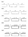
FIGS. 3 to 15 are cross-sectional views sequentially illustrating each of stages in a method of manufacturing a solar cell according to an example embodiment. - As shown in
FIG. 3 , a plurality of viaholes 181 are formed on asubstrate 110 formed of p-type single crystal silicon or p-type polycrystalline silicon. The via holes 181 are formed through a laser drilling method using a laser beam. Other methods may be used for forming the via holes 181. - As shown in
FIG. 4 , a texturing process is performed on the entire surface of thesubstrate 110 to form a textured surface of thesubstrate 110. However, a side wall of each of the via holes 181 need not have the textured surface, though such may be optional. When thesubstrate 110 is formed of p-type single crystal silicon, the texturing process is performed using a basic solution such as KOH, NaOH, and tetramethylammonium hydroxide (TMAH). When thesubstrate 110 is formed of p-type polycrystalline silicon, the texturing process is performed using an acid solution such as HF and HNO3. - As shown in
FIG. 5 , a high temperature thermal process of a material (for example, POCl3 or H3PO4) containing impurities of a group V element such as P, As, and Sb is performed on thesubstrate 110 to distribute the group V element impurities on thesubstrate 110. Hence, anemitter layer 120 is formed on the entire surface of thesubstrate 110 including a front surface, a rear surface, and an inner surface of thesubstrate 110 and/or a side surface (or side walls) of each of the via holes 181. Unlike the embodiment, when thesubstrate 110 is of an n-type, a high temperature thermal process of a material (for example, B2H6) containing group III element impurities is performed on thesubstrate 110 or the material containing the group III element impurities is stacked on thesubstrate 110 to form the p-type emitter layer 120 on the entire surface of thesubstrate 110. Then, phosphorous silicate glass (PSG) containing phosphor (P) or boron silicate glass (BSG) containing boron (B) produced when p-type impurities or n-type impurities are distributed inside thesubstrate 110 are removed through an etching process. - As shown in
FIG. 6 , ananti-reflection layer 130 is formed on the front surface of thesubstrate 110 and at the side wall of each of the via holes 181 using a chemical vapor deposition (CVD) method such as a plasma enhanced chemical vapor deposition (PECVD) method. In addition, theanti-reflection layer 130 may be formed inside the via holes 181. - As shown in
FIG. 7 , a portion of the rear surface of thesubstrate 110 is removed using a wet or dry etching method, and thus a portion of theemitter layer 120 on the rear surface of thesubstrate 110 is removed. In this case, theemitter layer 120 and/oranti-reflection layer 130 formed at the side wall of the via holes 181 may be partially removed. - Alternatively, a removing operation for the portion of the rear surface of the
substrate 110 may be avoided or omitted if the emitter layer is not formed on the rear surface of thesubstrate 110. That is, instead of forming theemitter layer 120 over the entire surface of thesubstrate 110, including the rear surface of thesubstrate 110, as shown inFIG. 5 , forming of theemitter layer 120 on the rear surface of thesubstrate 110 may be avoided or omitted by using a mask or a barrier layer on the rear surface of thesubstrate 110. The mask or the barrier layer then may be removed, for example, by a separate etching operation. - As shown in
FIGS. 8 to 10 , afirst passivation layer 191 formed of silicon oxide (SiO x), asecond passivation layer 192 formed of silicon nitride (SiNx), and athird passivation layer 193 formed of silicon oxynitride (SiOxNy) are sequentially formed on the rear surface of thesubstrate 110 in the order named using the CVD method such as the PECVD method to complete apassivation layer 190. The first and third passivation layers 191 and 193 each have a thickness of about 200 nm, and thesecond passivation layer 192 has a thickness of about 20 nm. In forming thepassivation layer 190, such as the first through third passivation layers 191-193, on the rear surface of thesubstrate 110, thepassivation layer 190, such as the first through third passivation layers 191-193, may also be deposited in the viahole 181 on the side wall thereof, in the same order as on the rear surface, though such is not required. In embodiments, not all of the first through third passivation layers 191-193 may need to be used or required. That is, components of thepassivation layer 190 within the viahole 181 or on the side wall of the viahole 181 may be different from components of thepassivation layer 190 on the rear surface of thesubstrate 110. Accordingly, thepassivation layer 190 or components thereof for the viahole 181 and thepassivation layer 190 or components thereof for the rear surface of thesubstrate 110 may be formed together or separately. - As shown in
FIG. 11 , a paste containing Ag is coated on a corresponding portion of thesubstrate 110 using a screen printing method and then is dried at about 120°C to 200°C to form a front electrodecurrent collector pattern 165 and a rear electrodecurrent collector pattern 166. - As shown in
FIG. 12 , a paste containing Ag is coated on a corresponding portion using the screen printing method and then is dried to form afront electrode pattern 140. The Ag-containing paste forming the front electrodecurrent collector pattern 165, the rear electrodecurrent collector pattern 166, and thefront electrode pattern 140 may include at least one selected from the group consisting of Ni, Cu, Al, Sn, Zn, In, Ti, Au, and a combination thereof, instead of Ag. Other conductive metal materials may be used. - As shown in
FIG. 13 , a paste containing Al is coated on a corresponding portion of thesubstrate 110 using the screen printing method and then is dried to form a rear electrodeconductive layer pattern 150. In this case, the rear electrodeconductive layer pattern 150 is formed in a remaining portion excluding a formation portion of the front electrodecurrent collector pattern 165 and the rear electrodecurrent collector pattern 166 from the rear surface of thesubstrate 110. In the embodiment, a formation order of thefront electrode pattern 140, the front electrodecurrent collector pattern 165, the rear electrodecurrent collector pattern 166, and the rear electrodeconductive layer pattern 150 may vary. - As shown in
FIG. 14 , a laser beam is irradiated onto a fixed portion of the rear electrodeconductive layer pattern 150 to formrear electrode patterns 153 formed of a molten mixture of components of the rear electrodeconductive layer pattern 150, thepassivation layer 190, and thesubstrate 110. - A wavelength of the laser beam used may be approximately 355 nm or 532 nm. When the wavelength of the laser beam is approximately 355 nm, an intensity of the laser beam is approximately 1W. When the wavelength of the laser beam is approximately 532 nm, an intensity of the laser beam is approximately 10W. The wavelength and the intensity of the laser beam used may vary depending on a thickness and a material of the rear electrode
conductive layer pattern 150, a material and the number of layers of thepassivation layer 190, etc. Further, the number of irradiation operations of the laser beam onto the same portion may vary depending on the thickness and the material of the rear electrodeconductive layer pattern 150, the material and the number of layers of thepassivation layer 190, etc. - As shown in
FIG. 15 , thesubstrate 110 including thefront electrode pattern 140, the front electrodecurrent collector pattern 165, the rear electrodecurrent collector pattern 166, and the rear electrodeconductive layer pattern 150 is fired at a temperature of about 750°C to 800°C to form a plurality offront electrodes 141, a plurality of front electrodecurrent collectors 161 electrically connected to thefront electrodes 141, a rear electrodeconductive layer 155 including a plurality ofrear electrodes 151, and a plurality of BSF layers 171. - More specifically, when a thermal process is performed, the plurality of
front electrodes 141, that pass through contact portions with theanti-reflection layer 130 and thefront electrode pattern 140 and contact theemitter layer 120, are formed due to elements such as Pb contained in thefront electrode pattern 140. In addition, therear electrode patterns 153 contact thesubstrate 110 to form the plurality ofrear electrodes 151. In this case, metal components contained in each of thepatterns layers - Further, when the thermal process is performed, Al contained in the
rear electrodes 151 is distributed to thesubstrate 110 contacting therear electrodes 151 to form the plurality of BSF layers 171 between therear electrodes 151 and thesubstrate 110. In this case, the BSF layers 171 are an area doped with impurities of the same conductive type as thesubstrate 110, for example, p-type impurities. An impurity doping concentration of the BSF layers 171 is greater than an impurity doping concentration of thesubstrate 110, and thus the BSF layers 171 are a p+-type area. - In the embodiment, because the
anti-reflection layer 130 and thepassivation layer 190 are formed at the side wall of each of the via holes 181, a damage of theemitter layer 120 generated when the high temperature thermal process including the drying and firing operations is performed can be reduced or prevented, and a generation of a leakage current can be reduced or prevented. Further, because thepassivation layer 190 has the multi-layered structure, the damage of theemitter layer 120 is further reduced or prevented. - Next, a plurality of exposing
portions 182 exposing a portion of thesubstrate 110 are formed around the front electrodecurrent collectors 161 using a laser beam to electrically separate therear electrodes 151 electrically connected to thesubstrate 110 from the front electrodecurrent collectors 161. The solar cell 1 shown inFIGS. 1 and 2 is completed thereby. Further, before and after the plurality of exposingportions 182 are formed, a portion of theanti-reflection layer 130 formed at an edge of the front surface of thesubstrate 110 and a portion of theemitter layer 120 underlying theanti-reflection layer 130 are removed to form an exposing portion (not shown) exposing a portion of the front surface of thesubstrate 110. Hence, an edge isolation of thesubstrate 110 is implemented through the exposing portion. In addition, the exposingportions 182 and the exposing portion used in the edge isolation may be formed using a PECVD method instead of the laser beam. - In the solar cell 1 manufactured through the above-described processes, the
anti-reflection layer 130 and thepassivation layer 190 may be non-uniformly formed at the side wall of the viahole 181 depending on a diameter of the viahole 181, a diffusion speed, a diffusion distance, a diffusion state, etc. when theanti-reflection layer 130 and thepassivation layer 190 are formed. Accordingly, as shown inFIG. 16 , the number of layers formed at the side wall of the viahole 181 may vary depending on a location of the side wall of the viahole 181. For example, the number of layers formed at the side wall of the viahole 181 increases in a portion adjacent to an injection location of a process gas in a vapor state used to form each of layers constituting thepassivation layer 190. Namely, the number of layers formed at the side wall of the viahole 181 increases as the side wall of the viahole 181 approaches the rear surface of thesubstrate 110. - Further, as shown in
FIG. 16 , even if the number of layers formed at the side wall of the viahole 181 is constant, a total thickness of layers formed at the side wall of the viahole 181 may vary depending on a the injection location of the process gas, i.e., depending on a distance (i.e., an injection distance) between the injection location of the process gas and the side wall of the viahole 181. Accordingly, the total thickness of layers formed at the side wall of the viahole 181 increases as the side wall of the viahole 181 approaches the rear surface of the substrate 110 (i.e., as the injection distance becomes shorter). However, in this case, because the side wall of the viahole 181 is protected by theanti-reflection layer 130 and thepassivation layer 190 including at least one layer, a generation of a leakage current resulting from the damage of theemitter layer 120 after the thermal process is reduced or prevented. During a fabrication of the solar cell 1 through the processes illustrated inFIGS. 3 to 15 , a portion of thesubstrate 110 may be exposed through the side wall of the viahole 181. - As shown in
FIG. 7 , when theemitter layer 120 on the rear surface of thesubstrate 110 is removed, a portion of theanti-reflection layer 130 inside the viahole 181 and a portion of theemitter layer 120 underlying theanti-reflection layer 130 may be removed. Hence, after a removing process of theemitter layer 120 on the rear surface of thesubstrate 110, a portion of thesubstrate 110 may be exposed through the side wall of the viahole 181. In this case, as theemitter layer 120 and theanti-reflection layer 130 approach the rear surface of thesubstrate 110, a probability to remove theemitter layer 120 and theanti-reflection layer 130 inside the viahole 181 together with theemitter layer 120 on the rear surface of thesubstrate 110 increases. However, in the embodiment, because thepassivation layer 190 having the multi-layered structure is positioned at the side wall of the viahole 181, as shown inFIG. 17 , the portion of the substrate 11 0 exposed at the side wall of the viahole 181 is covered by theantireflection layer 130 in a subsequent process. - As shown in
FIG. 16 , because a formation of thepassivation layer 190 is easily performed at the rear surface of thesubstrate 110 having a high removing probability of theemitter layer 120, the exposed portion of thesubstrate 110 through at the side wall of the viahole 181 is easily covered by thepassivation layer 190. Accordingly, even if the portion of theemitter layer 120 and the portion of theanti-reflection layer 130 are damaged and the portion of the substrate 11 0 is exposed at the side wall of the viahole 181, the exposed portion of thesubstrate 110 is protected by thepassivation layer 190. Hence, a leakage phenomenon of a current flowing from thefront electrode 141 to the front electrodecurrent collector 161 is reduced. - In embodiments of the invention, reference to front or back, with respect to electrode, a surface of the substrate, or others is not limiting. For example, such a reference is for convenience of description since front or back is easily understood as examples of first or second of the electrode, the surface of the substrate or others.
- While this invention has been described in connection with what is presently considered to be practical example embodiments, it is to be understood that the invention is not limited to the disclosed embodiments, but, on the contrary, is intended to cover various modifications and equivalent arrangements included within the scope of the appended claims.
Claims (10)
- A solar cell (1), comprising:a substrate (110) of a first conductive type having at least one via hole (181);an emitter layer (120) only on at least a portion of the at least one via hole (181) and at least one selected from a group consisting of an incident surface and side surfaces of the substrate (110), the emitter layer (120) having a second conductive type opposite the first conductive type;at least one first electrode (141) on the incident surface of the substrate (110), the first electrode (141) being electrically connected to the emitter layer (120);a second electrode (151) connected to an opposite surface to the incident surface of the substrate (120);at least one first electrode current collector (161) on the opposite surface, the at least one first electrode current collector (161) being insulated from the second electrode (151) and being electrically connected to the at least one first electrode (141) through the at least one via hole (181); anda passivation layer (190) on the opposite surface of the substrate (110) and on at least a portion of a side wall of the at least one via hole (181),characterized in that the passivation layer (190) includes a first passivation layer (191) on the opposite surface of the substrate (110), a second passivation layer (192) on the first passivation layer (191), and a third passivation layer (193) on the second passivation layer (192), andeach of the first, second, and third passivation layers (191-193) is formed of one of silicon oxide, silicon nitride, silicon oxynitride, or amorphous silicon.
- The solar cell of claim 1, wherein the first passivation layer (191) is formed of silicon oxide, the second passivation layer (192) is formed of silicon nitride, and the third passivation layer (192) is formed of silicon oxynitride.
- The solar cell of claim 1, wherein each of the first, second, and third passivation layers (191-193) has a different refractive index.
- The solar cell of claim 3, wherein the first passivation layer (191) has a minimum refractive index of the first, second, and third passivation layers (191-193), and the second passivation layer (192) has a maximum refractive index of the first, second, and third passivation layers.
- The solar cell of claim 1, wherein the thickness of the passivation layer (190) formed at the side wall of the at least one via hole (181) increases as the side wall of the at least one via hole (181) approaches the opposite surface of the substrate (110).
- The solar cell of claim 5, wherein a number of layers constituting the passivation layer (190) formed at the side wall of the at least one via hole (181) increases as the side wall of the at least one via hole approaches the opposite surface of the substrate (110).
- The solar cell of claim 1, wherein the emitter layer (120) is positioned at a side wall of the at least one via hole (181).
- The solar cell of claim 1, further comprising an anti-reflection layer (130) between the emitter layer (120) and the passivation layer (190).
- The solar cell of claim 8, wherein the anti-reflection layer (130) is formed of silicon oxide or silicon nitride.
- The solar cell of claim 1, further comprising at least one second electrode current collector (162) electrically connected to the second electrode (151).
Applications Claiming Priority (2)
| Application Number | Priority Date | Filing Date | Title |
|---|---|---|---|
| KR1020090055379A KR101032624B1 (en) | 2009-06-22 | 2009-06-22 | Solar cell and mehtod for manufacturing the same |
| PCT/KR2009/005051 WO2010150943A1 (en) | 2009-06-22 | 2009-09-07 | Solar cell and method of manufacturing the same |
Publications (3)
| Publication Number | Publication Date |
|---|---|
| EP2371010A1 EP2371010A1 (en) | 2011-10-05 |
| EP2371010A4 EP2371010A4 (en) | 2013-10-09 |
| EP2371010B1 true EP2371010B1 (en) | 2014-11-05 |
Family
ID=42933370
Family Applications (1)
| Application Number | Title | Priority Date | Filing Date |
|---|---|---|---|
| EP09846574.3A Not-in-force EP2371010B1 (en) | 2009-06-22 | 2009-09-07 | Solar cell and method of manufacturing the same |
Country Status (6)
| Country | Link |
|---|---|
| US (3) | US8203072B2 (en) |
| EP (1) | EP2371010B1 (en) |
| JP (1) | JP5302414B2 (en) |
| KR (1) | KR101032624B1 (en) |
| CN (1) | CN102292825B (en) |
| WO (1) | WO2010150943A1 (en) |
Families Citing this family (62)
| Publication number | Priority date | Publication date | Assignee | Title |
|---|---|---|---|---|
| US8815104B2 (en) | 2008-03-21 | 2014-08-26 | Alliance For Sustainable Energy, Llc | Copper-assisted, anti-reflection etching of silicon surfaces |
| JP5185157B2 (en) * | 2009-02-25 | 2013-04-17 | 浜松ホトニクス株式会社 | Photodiode manufacturing method and photodiode |
| JP5643293B2 (en) | 2009-04-21 | 2014-12-17 | テトラサン インコーポレイテッド | Method for forming a structure in a solar cell |
| WO2010147260A1 (en) * | 2009-06-18 | 2010-12-23 | Lg Electronics Inc. | Solar cell and method of manufacturing the same |
| CN102388465B (en) * | 2009-09-29 | 2014-11-05 | 京瓷株式会社 | Solar cell element and solar cell module |
| TWI415277B (en) * | 2009-11-20 | 2013-11-11 | Ind Tech Res Inst | Solar cell structure |
| KR101579318B1 (en) * | 2010-04-29 | 2015-12-21 | 엘지전자 주식회사 | Solar cell and method for manufacturing the same |
| US20130089944A1 (en) * | 2010-06-11 | 2013-04-11 | Amtech Systems, Inc. | Solar cell silicon wafer process |
| DE102010026960A1 (en) * | 2010-07-12 | 2012-01-12 | Fraunhofer-Gesellschaft zur Förderung der angewandten Forschung e.V. | Photovoltaic solar cell and method for producing a photovoltaic solar cell |
| NL2005261C2 (en) | 2010-08-24 | 2012-02-27 | Solland Solar Cells B V | Back contacted photovoltaic cell with an improved shunt resistance. |
| KR101624989B1 (en) * | 2010-09-10 | 2016-05-27 | 주식회사 원익아이피에스 | Surface processing method of silicon substrate for solar cell, and manufacturing method of solar cell |
| KR101275575B1 (en) * | 2010-10-11 | 2013-06-14 | 엘지전자 주식회사 | Back contact solar cell and manufacturing method thereof |
| TWI435454B (en) * | 2010-10-25 | 2014-04-21 | Au Optronics Corp | Solar cell |
| KR101699310B1 (en) * | 2010-12-17 | 2017-02-13 | 엘지전자 주식회사 | Solar cell and method for manufacturing the same |
| KR101729745B1 (en) * | 2011-01-05 | 2017-04-24 | 엘지전자 주식회사 | Solar cell and manufacturing method thereof |
| CN102593204B (en) * | 2011-01-10 | 2014-09-24 | Lg电子株式会社 | Solar cell and method for manufacturing the same |
| KR101745683B1 (en) * | 2011-01-14 | 2017-06-09 | 엘지전자 주식회사 | Solar cell and method for manufacturing the same |
| KR20120084104A (en) * | 2011-01-19 | 2012-07-27 | 엘지전자 주식회사 | Solar cell |
| CN102610661A (en) * | 2011-01-25 | 2012-07-25 | 东方电气集团(宜兴)迈吉太阳能科技有限公司 | Lamination-recombination passive film used for front surface of single-crystalline-silicon solar cell |
| CN102610662A (en) * | 2011-01-25 | 2012-07-25 | 东方电气集团(宜兴)迈吉太阳能科技有限公司 | Laminated composite passivation film used on back surface of monocrystalline silicon solar cell |
| NL2006161C2 (en) * | 2011-02-08 | 2012-08-09 | Tsc Solar B V | Method of manufacturing a solar cell and solar cell thus obtained. |
| CN103283001A (en) * | 2011-03-08 | 2013-09-04 | 可持续能源联盟有限责任公司 | Efficient black silicon photovoltaic devices with enhanced blue response |
| KR20120111378A (en) * | 2011-03-31 | 2012-10-10 | 삼성디스플레이 주식회사 | Solar cell and fabrication method of the same |
| CN102800741B (en) * | 2011-05-27 | 2015-04-15 | 苏州阿特斯阳光电力科技有限公司 | Method for manufacturing back contact crystalline silicon solar battery piece |
| CN102800743B (en) * | 2011-05-27 | 2015-12-02 | 苏州阿特斯阳光电力科技有限公司 | Back contacts crystal silicon solar cell sheet manufacture method |
| US9153713B2 (en) | 2011-04-02 | 2015-10-06 | Csi Cells Co., Ltd | Solar cell modules and methods of manufacturing the same |
| US8916410B2 (en) | 2011-05-27 | 2014-12-23 | Csi Cells Co., Ltd | Methods of manufacturing light to current converter devices |
| KR101738000B1 (en) * | 2011-06-20 | 2017-05-19 | 엘지전자 주식회사 | Solar cell and method for manufacturing the same |
| KR101278441B1 (en) * | 2011-08-31 | 2013-07-01 | 한화케미칼 주식회사 | Fabrication Method of Emitter Wrap Through Solar Cell Using One―step Doping Process |
| CN102386249B (en) * | 2011-10-31 | 2013-08-14 | 北京吉阳技术股份有限公司 | High-efficiency crystalline silicon cell with next-generation structure and manufacturing method for high-efficiency crystalline silicon cell |
| CN102361040A (en) * | 2011-11-08 | 2012-02-22 | 天威新能源控股有限公司 | Solar cell and preparation method thereof |
| KR101295552B1 (en) | 2011-11-16 | 2013-08-12 | 엘지전자 주식회사 | Solar cell and method for manufacturing the same |
| CN102544235A (en) * | 2012-02-24 | 2012-07-04 | 上饶光电高科技有限公司 | Preparation method for MWT solar battery electrode |
| CN102709336A (en) * | 2012-04-27 | 2012-10-03 | 苏州阿特斯阳光电力科技有限公司 | Back electrode structure of back contact solar cell |
| NL2008970C2 (en) * | 2012-06-08 | 2013-12-10 | Tempress Ip B V | Method of manufacturing a solar cell and solar cell thus obtained. |
| KR101921738B1 (en) * | 2012-06-26 | 2018-11-23 | 엘지전자 주식회사 | Solar cell |
| JP6187053B2 (en) | 2012-09-18 | 2017-08-30 | 株式会社リコー | Information processing system, information processing apparatus, and program |
| CN103022160B (en) * | 2013-01-10 | 2015-11-18 | 常州天合光能有限公司 | The solar cell passivated reflection reducing membrane of the anti-PID effect of energy |
| CN103258915A (en) * | 2013-05-31 | 2013-08-21 | 英利集团有限公司 | MWT solar battery piece and manufacturing method thereof |
| CN203423193U (en) * | 2013-07-08 | 2014-02-05 | 南京日托光伏科技有限公司 | MWT solar cell |
| CN103594529A (en) * | 2013-11-27 | 2014-02-19 | 奥特斯维能源(太仓)有限公司 | MWT and passivation combined crystal silicon solar cell and manufacturing method thereof |
| US9218958B2 (en) | 2013-12-10 | 2015-12-22 | Infineon Technologies Ag | Method for forming a semiconductor device |
| US9570576B2 (en) * | 2013-12-10 | 2017-02-14 | Infineon Technologies Ag | Method for forming a semiconductor device having insulating parts or layers formed via anodic oxidation |
| WO2015118592A1 (en) * | 2014-02-06 | 2015-08-13 | パナソニックIpマネジメント株式会社 | Solar cell and solar cell manufacturing method |
| US9716192B2 (en) * | 2014-03-28 | 2017-07-25 | International Business Machines Corporation | Method for fabricating a photovoltaic device by uniform plating on emitter-lined through-wafer vias and interconnects |
| CN104377268A (en) * | 2014-07-01 | 2015-02-25 | 安徽旭腾光伏电力有限公司 | Solar cell panel and crystal silicon wafer thereof |
| US20160284917A1 (en) * | 2015-03-27 | 2016-09-29 | Seung Bum Rim | Passivation Layer for Solar Cells |
| KR102550458B1 (en) * | 2015-05-13 | 2023-07-04 | 상라오 징코 솔라 테크놀러지 디벨롭먼트 컴퍼니, 리미티드 | Solar cell and method for manufacturing the same |
| CN105161569A (en) * | 2015-08-18 | 2015-12-16 | 英利能源(中国)有限公司 | MWT (metal wrap through) solar cell and preparation method therefor |
| WO2017078164A1 (en) * | 2015-11-04 | 2017-05-11 | 株式会社カネカ | Method for manufacturing crystalline silicon-based solar cell and method for manufacturing crystalline silicon-based solar cell module |
| CN107611183B (en) * | 2016-06-30 | 2020-06-19 | 比亚迪股份有限公司 | Cell, cell matrix, solar cell and preparation method of cell |
| CN106409926A (en) * | 2016-11-30 | 2017-02-15 | 庞倩桃 | Multilayer passivation film of crystalline-silicon battery and manufacturing method thereof |
| CN107425085A (en) * | 2017-03-30 | 2017-12-01 | 陈文英 | A kind of preparation method of the back contacts crystal silicon solar batteries of passivating back |
| CN107564988B (en) * | 2017-09-05 | 2021-06-25 | 北京普扬科技有限公司 | MWT battery and preparation method thereof |
| WO2019204119A1 (en) * | 2018-04-16 | 2019-10-24 | Sunpower Corporation | Solar cells having junctions retracted from cleaved edges |
| DE102019006099B4 (en) * | 2019-08-29 | 2022-03-17 | Azur Space Solar Power Gmbh | Stacked multi-junction solar cell with metallization comprising a multi-layer system |
| DE102019006097A1 (en) * | 2019-08-29 | 2021-03-04 | Azur Space Solar Power Gmbh | Passivation process for a through hole in a semiconductor wafer |
| DE102019006096A1 (en) * | 2019-08-29 | 2021-03-04 | Azur Space Solar Power Gmbh | Stacked multi-junction solar cell with a dielectric insulation layer system |
| CN111668317B (en) * | 2020-05-29 | 2021-09-24 | 晶科绿能(上海)管理有限公司 | Photovoltaic module, solar cell and preparation method thereof |
| CN111668318B (en) * | 2020-05-29 | 2021-09-24 | 晶科绿能(上海)管理有限公司 | Photovoltaic module, solar cell and preparation method thereof |
| CN116314356A (en) * | 2021-02-23 | 2023-06-23 | 浙江晶科能源有限公司 | Solar cell, manufacturing method thereof and solar module |
| CN115132851B (en) * | 2021-08-26 | 2023-06-16 | 上海晶科绿能企业管理有限公司 | Solar cell, manufacturing method thereof and photovoltaic module |
Family Cites Families (26)
| Publication number | Priority date | Publication date | Assignee | Title |
|---|---|---|---|---|
| US3903428A (en) * | 1973-12-28 | 1975-09-02 | Hughes Aircraft Co | Solar cell contact design |
| US3903427A (en) * | 1973-12-28 | 1975-09-02 | Hughes Aircraft Co | Solar cell connections |
| DE3536299A1 (en) * | 1985-10-11 | 1987-04-16 | Nukem Gmbh | SOLAR CELL MADE OF SILICON |
| JPS6482570A (en) * | 1987-09-24 | 1989-03-28 | Mitsubishi Electric Corp | Manufacture of photoelectric conversion device |
| US4838952A (en) * | 1988-04-29 | 1989-06-13 | Spectrolab, Inc. | Controlled reflectance solar cell |
| US5380553A (en) * | 1990-12-24 | 1995-01-10 | Dow Corning Corporation | Reverse direction pyrolysis processing |
| JPH04276665A (en) * | 1991-03-04 | 1992-10-01 | Canon Inc | Integrated solar battery |
| JP2755281B2 (en) * | 1992-12-28 | 1998-05-20 | 富士電機株式会社 | Thin film solar cell and method of manufacturing the same |
| US5468988A (en) * | 1994-03-04 | 1995-11-21 | United Solar Systems Corporation | Large area, through-hole, parallel-connected photovoltaic device |
| EP0881694A1 (en) * | 1997-05-30 | 1998-12-02 | Interuniversitair Micro-Elektronica Centrum Vzw | Solar cell and process of manufacturing the same |
| JP2001068693A (en) | 1999-08-25 | 2001-03-16 | Hitachi Cable Ltd | Solar cell |
| JP2003142579A (en) * | 2001-11-07 | 2003-05-16 | Hitachi Ltd | Semiconductor device and method for manufacturing the same |
| CN100454584C (en) * | 2003-01-10 | 2009-01-21 | 株式会社钟化 | Transparent thin-film solar cell module and its manufacturing method |
| US7656001B2 (en) * | 2006-11-01 | 2010-02-02 | Udt Sensors, Inc. | Front-side illuminated, back-side contact double-sided PN-junction photodiode arrays |
| US20060060238A1 (en) * | 2004-02-05 | 2006-03-23 | Advent Solar, Inc. | Process and fabrication methods for emitter wrap through back contact solar cells |
| US7144751B2 (en) * | 2004-02-05 | 2006-12-05 | Advent Solar, Inc. | Back-contact solar cells and methods for fabrication |
| US20060130891A1 (en) * | 2004-10-29 | 2006-06-22 | Carlson David E | Back-contact photovoltaic cells |
| KR100682017B1 (en) * | 2004-12-16 | 2007-02-12 | 주식회사 실트론 | Solar cell and method for manufacturing the same |
| US20070023082A1 (en) * | 2005-07-28 | 2007-02-01 | Venkatesan Manivannan | Compositionally-graded back contact photovoltaic devices and methods of fabricating such devices |
| KR101212198B1 (en) * | 2006-04-06 | 2012-12-13 | 삼성에스디아이 주식회사 | Solar cell |
| JP5025184B2 (en) | 2006-07-28 | 2012-09-12 | 京セラ株式会社 | Solar cell element, solar cell module using the same, and manufacturing method thereof |
| KR20080032866A (en) * | 2006-10-11 | 2008-04-16 | 삼성에스디아이 주식회사 | Mentalization wrap through type solar cell |
| JP5103038B2 (en) * | 2007-03-14 | 2012-12-19 | シャープ株式会社 | Photoelectric conversion element, solar cell module, solar power generation system |
| JP2008294080A (en) * | 2007-05-22 | 2008-12-04 | Sanyo Electric Co Ltd | Solar cell and manufacturing method of same |
| NL2001015C2 (en) * | 2007-11-19 | 2009-05-20 | Energieonderzoek Ct Nederland | Method for fabricating a rear-contact photovoltaic cell, and rear-contact photovoltaic cell made by such a method. |
| WO2009066583A1 (en) * | 2007-11-22 | 2009-05-28 | Sharp Kabushiki Kaisha | Wiring member between elements, photoelectric conversion element, and photoelectric conversion element connecting body and photoelectric conversion module using the wiring member between elements and the photoelectric conversion element |
-
2009
- 2009-06-22 KR KR1020090055379A patent/KR101032624B1/en active IP Right Grant
- 2009-09-07 EP EP09846574.3A patent/EP2371010B1/en not_active Not-in-force
- 2009-09-07 JP JP2011543385A patent/JP5302414B2/en not_active Expired - Fee Related
- 2009-09-07 CN CN200980155217.7A patent/CN102292825B/en not_active Expired - Fee Related
- 2009-09-07 WO PCT/KR2009/005051 patent/WO2010150943A1/en active Application Filing
- 2009-09-15 US US12/559,542 patent/US8203072B2/en active Active
-
2012
- 2012-05-18 US US13/475,659 patent/US8507789B2/en active Active
- 2012-05-18 US US13/475,680 patent/US8481847B2/en active Active
Also Published As
| Publication number | Publication date |
|---|---|
| JP2012513685A (en) | 2012-06-14 |
| CN102292825B (en) | 2014-09-03 |
| CN102292825A (en) | 2011-12-21 |
| EP2371010A4 (en) | 2013-10-09 |
| KR20100137117A (en) | 2010-12-30 |
| US8203072B2 (en) | 2012-06-19 |
| US8507789B2 (en) | 2013-08-13 |
| US20120264252A1 (en) | 2012-10-18 |
| US20120227804A1 (en) | 2012-09-13 |
| KR101032624B1 (en) | 2011-05-06 |
| WO2010150943A1 (en) | 2010-12-29 |
| EP2371010A1 (en) | 2011-10-05 |
| JP5302414B2 (en) | 2013-10-02 |
| US20100258177A1 (en) | 2010-10-14 |
| US8481847B2 (en) | 2013-07-09 |
Similar Documents
| Publication | Publication Date | Title |
|---|---|---|
| EP2371010B1 (en) | Solar cell and method of manufacturing the same | |
| US8569614B2 (en) | Solar cell and method of manufacturing the same | |
| EP2371009B1 (en) | Solar cell and method of manufacturing the same | |
| US9306084B2 (en) | Solar cell and method of manufacturing the same | |
| EP3297038B1 (en) | Solar cell | |
| US9825190B2 (en) | Solar cell and method for manufacturing the same | |
| KR101714779B1 (en) | Solar cell and manufacturing method thereof | |
| EP3379583B1 (en) | Method of manufacturing a solar cell | |
| KR101135585B1 (en) | Solar cell and method for manufacturing the same | |
| KR101588458B1 (en) | Solar cell and manufacturing mehtod of the same | |
| KR101199649B1 (en) | Localized Emitter Solar Cell and Method for Manufacturing Thereof | |
| KR101114198B1 (en) | Localized emitter solar cell and method for manufacturing thereof | |
| KR101199213B1 (en) | Bifacial Photovoltaic Localized Emitter Solar Cell and Method for Manufacturing Thereof | |
| KR101173399B1 (en) | Localized Emitter Solar Cell and Method for Manufacturing Thereof | |
| KR20110138648A (en) | Solar cell and method for manufacturing the same | |
| KR20120031693A (en) | Solar cell and method for manufacturing the same |
Legal Events
| Date | Code | Title | Description |
|---|---|---|---|
| PUAI | Public reference made under article 153(3) epc to a published international application that has entered the european phase |
Free format text: ORIGINAL CODE: 0009012 |
|
| 17P | Request for examination filed |
Effective date: 20110615 |
|
| AK | Designated contracting states |
Kind code of ref document: A1 Designated state(s): AT BE BG CH CY CZ DE DK EE ES FI FR GB GR HR HU IE IS IT LI LT LU LV MC MK MT NL NO PL PT RO SE SI SK SM TR |
|
| DAX | Request for extension of the european patent (deleted) | ||
| REG | Reference to a national code |
Ref country code: DE Ref legal event code: R079 Ref document number: 602009027644 Country of ref document: DE Free format text: PREVIOUS MAIN CLASS: H01L0031042000 Ipc: H01L0031021600 |
|
| A4 | Supplementary search report drawn up and despatched |
Effective date: 20130910 |
|
| RIC1 | Information provided on ipc code assigned before grant |
Ipc: H01L 31/0224 20060101ALI20130904BHEP Ipc: H01L 31/0216 20060101AFI20130904BHEP Ipc: H01L 31/068 20120101ALI20130904BHEP |
|
| GRAP | Despatch of communication of intention to grant a patent |
Free format text: ORIGINAL CODE: EPIDOSNIGR1 |
|
| INTG | Intention to grant announced |
Effective date: 20140513 |
|
| GRAS | Grant fee paid |
Free format text: ORIGINAL CODE: EPIDOSNIGR3 |
|
| GRAA | (expected) grant |
Free format text: ORIGINAL CODE: 0009210 |
|
| AK | Designated contracting states |
Kind code of ref document: B1 Designated state(s): AT BE BG CH CY CZ DE DK EE ES FI FR GB GR HR HU IE IS IT LI LT LU LV MC MK MT NL NO PL PT RO SE SI SK SM TR |
|
| REG | Reference to a national code |
Ref country code: GB Ref legal event code: FG4D |
|
| REG | Reference to a national code |
Ref country code: CH Ref legal event code: EP |
|
| REG | Reference to a national code |
Ref country code: AT Ref legal event code: REF Ref document number: 695000 Country of ref document: AT Kind code of ref document: T Effective date: 20141115 |
|
| REG | Reference to a national code |
Ref country code: IE Ref legal event code: FG4D |
|
| REG | Reference to a national code |
Ref country code: DE Ref legal event code: R096 Ref document number: 602009027644 Country of ref document: DE Effective date: 20141218 |
|
| REG | Reference to a national code |
Ref country code: NL Ref legal event code: T3 |
|
| REG | Reference to a national code |
Ref country code: AT Ref legal event code: MK05 Ref document number: 695000 Country of ref document: AT Kind code of ref document: T Effective date: 20141105 |
|
| REG | Reference to a national code |
Ref country code: LT Ref legal event code: MG4D |
|
| PG25 | Lapsed in a contracting state [announced via postgrant information from national office to epo] |
Ref country code: NO Free format text: LAPSE BECAUSE OF FAILURE TO SUBMIT A TRANSLATION OF THE DESCRIPTION OR TO PAY THE FEE WITHIN THE PRESCRIBED TIME-LIMIT Effective date: 20150205 Ref country code: LT Free format text: LAPSE BECAUSE OF FAILURE TO SUBMIT A TRANSLATION OF THE DESCRIPTION OR TO PAY THE FEE WITHIN THE PRESCRIBED TIME-LIMIT Effective date: 20141105 Ref country code: PT Free format text: LAPSE BECAUSE OF FAILURE TO SUBMIT A TRANSLATION OF THE DESCRIPTION OR TO PAY THE FEE WITHIN THE PRESCRIBED TIME-LIMIT Effective date: 20150305 Ref country code: IS Free format text: LAPSE BECAUSE OF FAILURE TO SUBMIT A TRANSLATION OF THE DESCRIPTION OR TO PAY THE FEE WITHIN THE PRESCRIBED TIME-LIMIT Effective date: 20150305 Ref country code: FI Free format text: LAPSE BECAUSE OF FAILURE TO SUBMIT A TRANSLATION OF THE DESCRIPTION OR TO PAY THE FEE WITHIN THE PRESCRIBED TIME-LIMIT Effective date: 20141105 |
|
| PG25 | Lapsed in a contracting state [announced via postgrant information from national office to epo] |
Ref country code: HR Free format text: LAPSE BECAUSE OF FAILURE TO SUBMIT A TRANSLATION OF THE DESCRIPTION OR TO PAY THE FEE WITHIN THE PRESCRIBED TIME-LIMIT Effective date: 20141105 Ref country code: AT Free format text: LAPSE BECAUSE OF FAILURE TO SUBMIT A TRANSLATION OF THE DESCRIPTION OR TO PAY THE FEE WITHIN THE PRESCRIBED TIME-LIMIT Effective date: 20141105 Ref country code: GR Free format text: LAPSE BECAUSE OF FAILURE TO SUBMIT A TRANSLATION OF THE DESCRIPTION OR TO PAY THE FEE WITHIN THE PRESCRIBED TIME-LIMIT Effective date: 20150206 Ref country code: PL Free format text: LAPSE BECAUSE OF FAILURE TO SUBMIT A TRANSLATION OF THE DESCRIPTION OR TO PAY THE FEE WITHIN THE PRESCRIBED TIME-LIMIT Effective date: 20141105 Ref country code: LV Free format text: LAPSE BECAUSE OF FAILURE TO SUBMIT A TRANSLATION OF THE DESCRIPTION OR TO PAY THE FEE WITHIN THE PRESCRIBED TIME-LIMIT Effective date: 20141105 Ref country code: SE Free format text: LAPSE BECAUSE OF FAILURE TO SUBMIT A TRANSLATION OF THE DESCRIPTION OR TO PAY THE FEE WITHIN THE PRESCRIBED TIME-LIMIT Effective date: 20141105 Ref country code: CY Free format text: LAPSE BECAUSE OF FAILURE TO SUBMIT A TRANSLATION OF THE DESCRIPTION OR TO PAY THE FEE WITHIN THE PRESCRIBED TIME-LIMIT Effective date: 20141105 |
|
| PG25 | Lapsed in a contracting state [announced via postgrant information from national office to epo] |
Ref country code: CZ Free format text: LAPSE BECAUSE OF FAILURE TO SUBMIT A TRANSLATION OF THE DESCRIPTION OR TO PAY THE FEE WITHIN THE PRESCRIBED TIME-LIMIT Effective date: 20141105 Ref country code: EE Free format text: LAPSE BECAUSE OF FAILURE TO SUBMIT A TRANSLATION OF THE DESCRIPTION OR TO PAY THE FEE WITHIN THE PRESCRIBED TIME-LIMIT Effective date: 20141105 Ref country code: DK Free format text: LAPSE BECAUSE OF FAILURE TO SUBMIT A TRANSLATION OF THE DESCRIPTION OR TO PAY THE FEE WITHIN THE PRESCRIBED TIME-LIMIT Effective date: 20141105 Ref country code: SK Free format text: LAPSE BECAUSE OF FAILURE TO SUBMIT A TRANSLATION OF THE DESCRIPTION OR TO PAY THE FEE WITHIN THE PRESCRIBED TIME-LIMIT Effective date: 20141105 Ref country code: RO Free format text: LAPSE BECAUSE OF FAILURE TO SUBMIT A TRANSLATION OF THE DESCRIPTION OR TO PAY THE FEE WITHIN THE PRESCRIBED TIME-LIMIT Effective date: 20141105 |
|
| REG | Reference to a national code |
Ref country code: DE Ref legal event code: R097 Ref document number: 602009027644 Country of ref document: DE |
|
| PLBE | No opposition filed within time limit |
Free format text: ORIGINAL CODE: 0009261 |
|
| STAA | Information on the status of an ep patent application or granted ep patent |
Free format text: STATUS: NO OPPOSITION FILED WITHIN TIME LIMIT |
|
| 26N | No opposition filed |
Effective date: 20150806 |
|
| PG25 | Lapsed in a contracting state [announced via postgrant information from national office to epo] |
Ref country code: IT Free format text: LAPSE BECAUSE OF FAILURE TO SUBMIT A TRANSLATION OF THE DESCRIPTION OR TO PAY THE FEE WITHIN THE PRESCRIBED TIME-LIMIT Effective date: 20141105 |
|
| PG25 | Lapsed in a contracting state [announced via postgrant information from national office to epo] |
Ref country code: SI Free format text: LAPSE BECAUSE OF FAILURE TO SUBMIT A TRANSLATION OF THE DESCRIPTION OR TO PAY THE FEE WITHIN THE PRESCRIBED TIME-LIMIT Effective date: 20141105 |
|
| PG25 | Lapsed in a contracting state [announced via postgrant information from national office to epo] |
Ref country code: MC Free format text: LAPSE BECAUSE OF FAILURE TO SUBMIT A TRANSLATION OF THE DESCRIPTION OR TO PAY THE FEE WITHIN THE PRESCRIBED TIME-LIMIT Effective date: 20141105 Ref country code: LU Free format text: LAPSE BECAUSE OF FAILURE TO SUBMIT A TRANSLATION OF THE DESCRIPTION OR TO PAY THE FEE WITHIN THE PRESCRIBED TIME-LIMIT Effective date: 20150907 |
|
| REG | Reference to a national code |
Ref country code: CH Ref legal event code: PL |
|
| GBPC | Gb: european patent ceased through non-payment of renewal fee |
Effective date: 20150907 |
|
| REG | Reference to a national code |
Ref country code: IE Ref legal event code: MM4A |
|
| REG | Reference to a national code |
Ref country code: FR Ref legal event code: ST Effective date: 20160531 |
|
| PG25 | Lapsed in a contracting state [announced via postgrant information from national office to epo] |
Ref country code: LI Free format text: LAPSE BECAUSE OF NON-PAYMENT OF DUE FEES Effective date: 20150930 Ref country code: GB Free format text: LAPSE BECAUSE OF NON-PAYMENT OF DUE FEES Effective date: 20150907 Ref country code: IE Free format text: LAPSE BECAUSE OF NON-PAYMENT OF DUE FEES Effective date: 20150907 Ref country code: CH Free format text: LAPSE BECAUSE OF NON-PAYMENT OF DUE FEES Effective date: 20150930 |
|
| PG25 | Lapsed in a contracting state [announced via postgrant information from national office to epo] |
Ref country code: FR Free format text: LAPSE BECAUSE OF NON-PAYMENT OF DUE FEES Effective date: 20150930 |
|
| PG25 | Lapsed in a contracting state [announced via postgrant information from national office to epo] |
Ref country code: MT Free format text: LAPSE BECAUSE OF FAILURE TO SUBMIT A TRANSLATION OF THE DESCRIPTION OR TO PAY THE FEE WITHIN THE PRESCRIBED TIME-LIMIT Effective date: 20141105 |
|
| PG25 | Lapsed in a contracting state [announced via postgrant information from national office to epo] |
Ref country code: HU Free format text: LAPSE BECAUSE OF FAILURE TO SUBMIT A TRANSLATION OF THE DESCRIPTION OR TO PAY THE FEE WITHIN THE PRESCRIBED TIME-LIMIT; INVALID AB INITIO Effective date: 20090907 Ref country code: SM Free format text: LAPSE BECAUSE OF FAILURE TO SUBMIT A TRANSLATION OF THE DESCRIPTION OR TO PAY THE FEE WITHIN THE PRESCRIBED TIME-LIMIT Effective date: 20141105 Ref country code: BG Free format text: LAPSE BECAUSE OF FAILURE TO SUBMIT A TRANSLATION OF THE DESCRIPTION OR TO PAY THE FEE WITHIN THE PRESCRIBED TIME-LIMIT Effective date: 20141105 |
|
| PG25 | Lapsed in a contracting state [announced via postgrant information from national office to epo] |
Ref country code: ES Free format text: LAPSE BECAUSE OF FAILURE TO SUBMIT A TRANSLATION OF THE DESCRIPTION OR TO PAY THE FEE WITHIN THE PRESCRIBED TIME-LIMIT Effective date: 20141105 |
|
| PG25 | Lapsed in a contracting state [announced via postgrant information from national office to epo] |
Ref country code: TR Free format text: LAPSE BECAUSE OF FAILURE TO SUBMIT A TRANSLATION OF THE DESCRIPTION OR TO PAY THE FEE WITHIN THE PRESCRIBED TIME-LIMIT Effective date: 20141105 |
|
| PG25 | Lapsed in a contracting state [announced via postgrant information from national office to epo] |
Ref country code: BE Free format text: LAPSE BECAUSE OF FAILURE TO SUBMIT A TRANSLATION OF THE DESCRIPTION OR TO PAY THE FEE WITHIN THE PRESCRIBED TIME-LIMIT Effective date: 20141105 |
|
| PGFP | Annual fee paid to national office [announced via postgrant information from national office to epo] |
Ref country code: NL Payment date: 20170810 Year of fee payment: 9 |
|
| PG25 | Lapsed in a contracting state [announced via postgrant information from national office to epo] |
Ref country code: MK Free format text: LAPSE BECAUSE OF FAILURE TO SUBMIT A TRANSLATION OF THE DESCRIPTION OR TO PAY THE FEE WITHIN THE PRESCRIBED TIME-LIMIT Effective date: 20141105 |
|
| PGFP | Annual fee paid to national office [announced via postgrant information from national office to epo] |
Ref country code: DE Payment date: 20180806 Year of fee payment: 10 |
|
| REG | Reference to a national code |
Ref country code: NL Ref legal event code: MM Effective date: 20181001 |
|
| PG25 | Lapsed in a contracting state [announced via postgrant information from national office to epo] |
Ref country code: NL Free format text: LAPSE BECAUSE OF NON-PAYMENT OF DUE FEES Effective date: 20181001 |
|
| REG | Reference to a national code |
Ref country code: DE Ref legal event code: R119 Ref document number: 602009027644 Country of ref document: DE |
|
| PG25 | Lapsed in a contracting state [announced via postgrant information from national office to epo] |
Ref country code: DE Free format text: LAPSE BECAUSE OF NON-PAYMENT OF DUE FEES Effective date: 20200401 |