EP2369623A2 - Light emitting device having several light emitting diodes and light unit having the same - Google Patents
Light emitting device having several light emitting diodes and light unit having the same Download PDFInfo
- Publication number
- EP2369623A2 EP2369623A2 EP11159496A EP11159496A EP2369623A2 EP 2369623 A2 EP2369623 A2 EP 2369623A2 EP 11159496 A EP11159496 A EP 11159496A EP 11159496 A EP11159496 A EP 11159496A EP 2369623 A2 EP2369623 A2 EP 2369623A2
- Authority
- EP
- European Patent Office
- Prior art keywords
- light emitting
- light
- wavelength
- main peak
- emitting diode
- Prior art date
- Legal status (The legal status is an assumption and is not a legal conclusion. Google has not performed a legal analysis and makes no representation as to the accuracy of the status listed.)
- Withdrawn
Links
- 229920005989 resin Polymers 0.000 claims description 13
- 239000011347 resin Substances 0.000 claims description 13
- OAICVXFJPJFONN-UHFFFAOYSA-N Phosphorus Chemical compound [P] OAICVXFJPJFONN-UHFFFAOYSA-N 0.000 claims description 11
- 238000001228 spectrum Methods 0.000 description 16
- 239000000758 substrate Substances 0.000 description 14
- 230000003287 optical effect Effects 0.000 description 11
- 239000010410 layer Substances 0.000 description 9
- 239000000463 material Substances 0.000 description 8
- 230000035945 sensitivity Effects 0.000 description 6
- XUIMIQQOPSSXEZ-UHFFFAOYSA-N Silicon Chemical compound [Si] XUIMIQQOPSSXEZ-UHFFFAOYSA-N 0.000 description 4
- 239000010408 film Substances 0.000 description 4
- 238000012986 modification Methods 0.000 description 4
- 230000004048 modification Effects 0.000 description 4
- 229910052710 silicon Inorganic materials 0.000 description 4
- 239000010703 silicon Substances 0.000 description 4
- 238000009792 diffusion process Methods 0.000 description 3
- 239000004065 semiconductor Substances 0.000 description 3
- 229910001218 Gallium arsenide Inorganic materials 0.000 description 2
- 229920000106 Liquid crystal polymer Polymers 0.000 description 2
- 239000004977 Liquid-crystal polymers (LCPs) Substances 0.000 description 2
- 239000004954 Polyphthalamide Substances 0.000 description 2
- 239000000853 adhesive Substances 0.000 description 2
- 230000001070 adhesive effect Effects 0.000 description 2
- 239000000919 ceramic Substances 0.000 description 2
- 239000011247 coating layer Substances 0.000 description 2
- 239000003086 colorant Substances 0.000 description 2
- 150000001875 compounds Chemical class 0.000 description 2
- PMHQVHHXPFUNSP-UHFFFAOYSA-M copper(1+);methylsulfanylmethane;bromide Chemical compound Br[Cu].CSC PMHQVHHXPFUNSP-UHFFFAOYSA-M 0.000 description 2
- 229910052751 metal Inorganic materials 0.000 description 2
- 239000002184 metal Substances 0.000 description 2
- 229920003229 poly(methyl methacrylate) Polymers 0.000 description 2
- 239000004926 polymethyl methacrylate Substances 0.000 description 2
- 229920006375 polyphtalamide Polymers 0.000 description 2
- 230000001681 protective effect Effects 0.000 description 2
- 229910000980 Aluminium gallium arsenide Inorganic materials 0.000 description 1
- 239000004593 Epoxy Substances 0.000 description 1
- 229910002601 GaN Inorganic materials 0.000 description 1
- 229910000530 Gallium indium arsenide Inorganic materials 0.000 description 1
- BQCADISMDOOEFD-UHFFFAOYSA-N Silver Chemical compound [Ag] BQCADISMDOOEFD-UHFFFAOYSA-N 0.000 description 1
- 101001045744 Sus scrofa Hepatocyte nuclear factor 1-beta Proteins 0.000 description 1
- 230000002159 abnormal effect Effects 0.000 description 1
- 229910010293 ceramic material Inorganic materials 0.000 description 1
- 239000012141 concentrate Substances 0.000 description 1
- 239000002019 doping agent Substances 0.000 description 1
- 230000000694 effects Effects 0.000 description 1
- 230000017525 heat dissipation Effects 0.000 description 1
- 239000004973 liquid crystal related substance Substances 0.000 description 1
- 239000011159 matrix material Substances 0.000 description 1
- 239000007769 metal material Substances 0.000 description 1
- 238000009877 rendering Methods 0.000 description 1
- HBMJWWWQQXIZIP-UHFFFAOYSA-N silicon carbide Chemical compound [Si+]#[C-] HBMJWWWQQXIZIP-UHFFFAOYSA-N 0.000 description 1
- 239000002210 silicon-based material Substances 0.000 description 1
- 229910052709 silver Inorganic materials 0.000 description 1
- 239000004332 silver Substances 0.000 description 1
- 239000002356 single layer Substances 0.000 description 1
- 239000010409 thin film Substances 0.000 description 1
Images

Classifications
-
- H—ELECTRICITY
- H01—ELECTRIC ELEMENTS
- H01L—SEMICONDUCTOR DEVICES NOT COVERED BY CLASS H10
- H01L25/00—Assemblies consisting of a plurality of individual semiconductor or other solid state devices ; Multistep manufacturing processes thereof
- H01L25/03—Assemblies consisting of a plurality of individual semiconductor or other solid state devices ; Multistep manufacturing processes thereof all the devices being of a type provided for in the same subgroup of groups H01L27/00 - H01L33/00, or in a single subclass of H10K, H10N, e.g. assemblies of rectifier diodes
- H01L25/04—Assemblies consisting of a plurality of individual semiconductor or other solid state devices ; Multistep manufacturing processes thereof all the devices being of a type provided for in the same subgroup of groups H01L27/00 - H01L33/00, or in a single subclass of H10K, H10N, e.g. assemblies of rectifier diodes the devices not having separate containers
- H01L25/075—Assemblies consisting of a plurality of individual semiconductor or other solid state devices ; Multistep manufacturing processes thereof all the devices being of a type provided for in the same subgroup of groups H01L27/00 - H01L33/00, or in a single subclass of H10K, H10N, e.g. assemblies of rectifier diodes the devices not having separate containers the devices being of a type provided for in group H01L33/00
- H01L25/0753—Assemblies consisting of a plurality of individual semiconductor or other solid state devices ; Multistep manufacturing processes thereof all the devices being of a type provided for in the same subgroup of groups H01L27/00 - H01L33/00, or in a single subclass of H10K, H10N, e.g. assemblies of rectifier diodes the devices not having separate containers the devices being of a type provided for in group H01L33/00 the devices being arranged next to each other
-
- H—ELECTRICITY
- H01—ELECTRIC ELEMENTS
- H01L—SEMICONDUCTOR DEVICES NOT COVERED BY CLASS H10
- H01L2224/00—Indexing scheme for arrangements for connecting or disconnecting semiconductor or solid-state bodies and methods related thereto as covered by H01L24/00
- H01L2224/01—Means for bonding being attached to, or being formed on, the surface to be connected, e.g. chip-to-package, die-attach, "first-level" interconnects; Manufacturing methods related thereto
- H01L2224/42—Wire connectors; Manufacturing methods related thereto
- H01L2224/47—Structure, shape, material or disposition of the wire connectors after the connecting process
- H01L2224/48—Structure, shape, material or disposition of the wire connectors after the connecting process of an individual wire connector
- H01L2224/4805—Shape
- H01L2224/4809—Loop shape
- H01L2224/48091—Arched
-
- H—ELECTRICITY
- H01—ELECTRIC ELEMENTS
- H01L—SEMICONDUCTOR DEVICES NOT COVERED BY CLASS H10
- H01L2924/00—Indexing scheme for arrangements or methods for connecting or disconnecting semiconductor or solid-state bodies as covered by H01L24/00
- H01L2924/10—Details of semiconductor or other solid state devices to be connected
- H01L2924/102—Material of the semiconductor or solid state bodies
- H01L2924/1025—Semiconducting materials
- H01L2924/10251—Elemental semiconductors, i.e. Group IV
- H01L2924/10253—Silicon [Si]
-
- H—ELECTRICITY
- H01—ELECTRIC ELEMENTS
- H01L—SEMICONDUCTOR DEVICES NOT COVERED BY CLASS H10
- H01L33/00—Semiconductor devices having potential barriers specially adapted for light emission; Processes or apparatus specially adapted for the manufacture or treatment thereof or of parts thereof; Details thereof
- H01L33/48—Semiconductor devices having potential barriers specially adapted for light emission; Processes or apparatus specially adapted for the manufacture or treatment thereof or of parts thereof; Details thereof characterised by the semiconductor body packages
- H01L33/50—Wavelength conversion elements
-
- H—ELECTRICITY
- H01—ELECTRIC ELEMENTS
- H01L—SEMICONDUCTOR DEVICES NOT COVERED BY CLASS H10
- H01L33/00—Semiconductor devices having potential barriers specially adapted for light emission; Processes or apparatus specially adapted for the manufacture or treatment thereof or of parts thereof; Details thereof
- H01L33/48—Semiconductor devices having potential barriers specially adapted for light emission; Processes or apparatus specially adapted for the manufacture or treatment thereof or of parts thereof; Details thereof characterised by the semiconductor body packages
- H01L33/62—Arrangements for conducting electric current to or from the semiconductor body, e.g. lead-frames, wire-bonds or solder balls
Definitions
- the embodiment relates to a light emitting device and a light unit having the same.
- a light emitting diode may constitute a light source for generating light by using GaAs, AlGaAs, GaN, InGaN, and InGaAlP-based compound semiconductor materials.
- Such an LED is packaged so as to be used as a light emitting device that emits lights having various colors.
- the light emitting device is used as a light source in various products such as a lighting indicator, a character indicator, and an image display.
- the embodiment provides a light emitting device having at least two light emitting diodes.
- the embodiment provides a light emitting device including light emitting diodes capable of emitting lights having the same color band and different main peaks.
- the embodiment provides a light unit including a plurality of light emitting device employing light emitting diodes capable of emitting lights having wavelength bands with different main peaks.
- a light emitting device includes a body; a first light emitting diode for emitting a light having a first main peak in a wavelength range of a first color; a second light emitting diode for emitting a light having a second main peak in the wavelength range of the first color; and a plurality of lead electrodes electrically connected to at least one of the first and second light emitting diodes on the body, wherein the first main peak of the first light emitting diode and the second main peak of the second light emitting diode have a wavelength difference of at least 75% based on the wavelength range of the first color.
- a light emitting device includes a body having a cavity; a first light emitting diode for emitting a light having a first main peak in a wavelength range of a first color band; a second light emitting diode for emitting a light having a second main peak in the wavelength range of the first color band; a plurality of lead electrodes electrically connected to at least one of the first and second light emitting diodes on the body; and a resin member disposed in the cavity, wherein a central peak of the first main peak of the first light emitting diode is closer to a short wavelength than to a central wavelength of the first color band, and a central peak of the second main peak of the second light emitting diode is closer to a long wavelength than to the central wavelength of the first color band.
- a light unit includes a board; and a plurality of light emitting devices arrayed on the board, wherein at least one first light emitting device of the light emitting devices includes a body; a first light emitting diode for emitting a light having a first main peak in a wavelength range of a first color; a second light emitting diode for emitting a light having a second main peak in the wavelength range of the first color; and a plurality of lead electrodes electrically connected to at least one of the first and second light emitting diodes on the body, and wherein the first main peak of the first light emitting diode and the second main peak of the second light emitting diode have a wavelength difference of at least 75% based on the wavelength range of the first color.
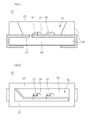
- FIG. 1 is a side sectional view showing a light emitting device according to the first embodiment
- FIG. 2 is a plan view of FIG. 1 ;
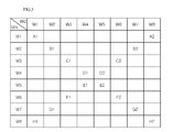
- FIG. 3 is a table showing an example of mixing of main peaks between light emitting devices according to the embodiment.
- FIG. 4 is a grapy showing an example of mixing of main peaks between light emitting devices shown in FIG. 1 ;
- FIG. 5 is a side sectional view showing a light emitting device package according to the second embodiment
- FIG. 6 is a side sectional view showing a light emitting device package according to the third embodiment.
- FIG. 7 is a view showing a light emitting module according to the fourth embodiment.
- FIG. 8 is a view showing a light emitting module according to the fifth embodiment.
- FIG. 9 is a side sectional view showing a display device according to the sixth embodiment.
- FIG. 10 is an exploded perspective view showing a display device according to the seventh embodiment.
- FIG. 11 is a graph showing spectrums of a plurality of light emitting devices in a light unit according to the embodiment.
- FIG. 12 is a perspective view showing a lighting unit including a light emitting device according to the embodiment.
- each layer shown in the drawings may be exaggerated, omitted or schematically drawn for the purpose of convenience or clarity.
- the size of elements does not utterly reflect an actual size.
- FIG. 1 is a side sectional view showing a light emitting device according to the first embodiment, and FIG. 2 is a plan view of FIG. 1 ;
- a light emitting device 10 includes a body 20 having a cavity 22 with an opened top surface, a plurality of lead electrodes 23 and 24, light emitting diodes 31 and 32 electrically connected to the lead electrodes 23 and 24, and a resin member 35 filled in the cavity 22.
- the body 20 may include one of a silicon material, a ceramic material and a resin material.
- the body 20 may include at least one of silicon, silicon carbide (SiC), aluminum nitride (A1N), polyphthalamide (PPA), and liquid crystal polymer (LCP), but the embodiment is not limited thereto.
- the body 20 can be prepared or injection-molded as a structure of a single-layer substrate or a multi-layer substrate, but the embodiment does not limit the shape and the structure of the body.
- the body 20 is formed at an upper portion thereof with the cavity 22 having the opening.
- the cavity 22 has a predetermined depth from the top surface of the body 20.
- the cavity 22 may have a concave cup shape or a concave tube shape having a predetermined curvature.
- a top surface of the cavity 22 may have a circular shape or a polygonal shape, but the embodiment is not limited thereto.
- An inner wall of the cavity 22 may be inclined toward a bottom surface of the cavity 22 to reflect the incident light toward the opening.
- the lead electrodes 23 and 24 are arranged at both sides of the body 20.
- the lead electrodes 23 and 24 are disposed at the lower surface of the body 20 to serve as external electrodes.
- the lead electrodes 23 and 24 are prepared as a lead frame type, a metal thin film type or a PCB (printed circuit board) pattern type.
- the lead frame type lead electrodes 23 and 24 will be described below.
- the light emitting diodes 31 and 32 are bonded to the second lead electrode 24 by an adhesive and electrically connected to the lead electrodes 23 and 24 by using a plurality of wires 34.
- the light emitting diodes 31 and 32 can be mounted by selectively using a die bonding scheme employing at least one wire or an adhesive, and a flip bonding scheme for reverse bonding of a chip. Such a bonding scheme may be selected according to the type of LED chips and the position of the electrode.
- the light emitting diodes 31 and 32 can be connected to the lead electrodes 23 and 24 in series or parallel, but the embodiment is not limited thereto.
- the light emitting diodes 31 and 32 may selectively include a semiconductor device manufactured by using a compound semiconductor, such as AlInGaN, InGaN, GaN, GaAs, InGaP, AlInGaP, InP, or InGaAs.
- the light emitting diodes 31 and 32 may include a blue LED chip, a yellow LED chip, a green LED chip, a red LED chip, a UV (ultraviolet) LED chip, a pumpkin-color LED chip, or a blue-green LED chip. Further, the number and type of the light emitting diodes 31 and 32 disposed in the light emitting device 10 can be changed and the light emitting diodes 31 and 32 may emit the light having the same color.
- the resin member 35 is filled in the cavity 22.
- the resin member 35 may include a transparent resin material, such as silicon or epoxy.
- a top surface of the resin member 35 may have a flat surface, a concave surface or a convex surface and a lens can be attached onto the resin member 35.
- the phosphor may include a yellow phosphor or a yellow/red phosphor.
- the phosphor is a yellow phosphor or a yellow/red phosphor.
- the light emitting device may include a protective device for protecting the light emitting diodes 31 and 32, but the embodiment is not limited thereto.
- the light emitting diodes 31 and 32 have the rank which is the reference for dividing the light emitting diodes 31 and 32 into groups or units. In detail, after the light emitted from the light emitting diodes 31 and 32 has been measured, the light emitting diodes 31 and 32 are divided into groups or units based on the chromatic rank, luminous rank and peak wavelength rank according to the characteristics of the light emitted from the light emitting diodes 31 and 32.
- the light emitting device 10 includes a plurality of light emitting diodes 31 and 32 which emit the spectrums having the same color wavelength band.
- the light emitting diodes 31 and 32 may represent different peak wavelengths.
- the light emitting diode 31 represents the first main peak which is closer to the short wavelength than to the central wavelength of the first color band
- the light emitting diode 32 represents the second main peak which is closer to the long wavelength than to the central wavelength of the first color band.
- the light emitting diode that emits the wavelength spectrum of blue light will be described as an example.
- the wavelength band of the blue light is about 380nm to about 500nm, preferably, about 380nm to about 480nm, more preferably, about 440nm to about 460nm.
- the short wavelength of the blue wavelength is about 380nm or less, preferably, about 440nm or less.
- the long wavelength of the blue wavelength is about 500nm or above, preferably, about 480nm or above, more preferably, about 460nm or above.
- the difference in wavelength between the first main peak of the first light emitting diode 31 and the second main peak of the second light emitting diode is about 75% or more within the wavelength range of one color.
- the difference in wavelength between the first main peak of the first light emitting diode 31 and the second main peak of the second light emitting diode can be represented as the difference between the central peak of the first main peak and the central peak of the second main peak.
- the difference in wavelength between the first main peak of the first light emitting diode 31 and the second main peak of the second light emitting diode can be represented as the actual wavelength difference, which is obtained by subtracting the second main peak from the first main peak.
- the difference is about 75% or above of 20nm, which is obtained by subtracting 440nm from 460nm, that is, about 15nm or above.
- the difference of 75% is about 7.5nm or above.
- the wavelength range of the red light is about 615nm to about 630nm, so the difference of 75% is about 11.25nm or above.
- the wavelength range of the yellow light is about 510nm to about 525nm, so the difference of 75% is about 11.25nm or above.
- the main peak may include the dominant wavelength or the FWHM (full width at half maximum).
- FIG. 3 is a table showing an example of mixing of main peaks between light emitting devices according to the embodiment.
- the blue wavelength band is in the range of about 440nm to about 460nm.
- the main peak of the blue wavelength can be obtained in the range of W1 to W8.
- Each main peak in W1 to W8 can be obtained at an interval of about 0.5nm to about 3.5nm, but the embodiment is not limited thereto.
- W1 is about 440nm to about 442.5nm
- W2 is about 442.5nm to about 445nm
- W3 is about 445nm to about 447.5nm
- W4 is about 447.5nm to about 450nm
- W5 is about 450nm to about 452.5nm
- W6 is about 452,5nm to about 455nm
- W7 is about 455nm to about 457.5nm
- W8 is about 457.5nm to about 460nm.
- the peak wavelengths of two light emitting diodes can be mixed with each other in the form of M1 to M8 by using A1 to A8 and A2 to H2.
- the embodiment may include two light emitting diodes (for instance, M1 and M8) representing great difference of the main peak.
- the first and second light emitting diodes 31 and 32 of the embodiment may be realized by mixing A1 and A2 or H2 and H1.
- the difference between the central peaks of the first and second light emitting diodes 31 and 32 may be about 10nm or above, preferably, about 15nm to about 20nm.
- the main peaks of the first and second light emitting diodes having the range of W1 and W8 are mixed so that the main peak Wx having the central peak W0 is represented.
- the central peak W0 is a peak in a set. For instance, when the central peak W0 is 450nm, the central peak W0 is in the range of 450nm ⁇ 1.25nm.
- the first main peak W1 of the first light emitting diode is a short wavelength spaced apart from the central peak (for instance, 450nm) by 37.5% or more
- the second main peak W8 of the second light emitting diode is a long wavelength spaced apart from the central peak (for instance, 450nm) by 37.5% or more. Since 37.5% is 7.5nm, the first and second main peaks W1 and W8 are spaced apart from the central peak W0 by 7.5nm, respectively.
- the first main peak W1 of the first light emitting diode is in the range of about 440nm to about 442.5nm and the second main peak W8 of the second light emitting diode is in the range of about 457.5nm to about 460nm.
- the difference T between the first main peak W1 of the first light emitting diode and the second main peak W8 of the second light emitting diode corresponds to the difference between the central peak of the first main peak and the central peak of the second main peak.
- the difference T between the central peaks of the first and second main peaks W1 and W8 is about 75% based on the wavelength range WR of the first color band.
- the central peaks of the first and second main peaks W1 and W8 are spaced apart from the central peak W0 of the first color band by about 37.5% in opposition to each other.
- the first main peak W1 of the first light emitting diode can be mixed with the second main peak W8 of the second light emitting diode in such a manner that the main peak Wx can be represented as the central peak in the set.
- the central peak may be a peak wavelength Wp or the actual central wavelength of the main peak.
- At least three light emitting diodes 31, 32 and 33 can be disposed in a light emitting device 10A as shown in FIG. 5 .
- the light emitting diodes 31, 32 and 33 may include first and second light emitting diodes 31 and 32 having the spectrum with the same color and representing the relatively great difference in wavelengths, and a third light emitting diode 33 having a peak wavelength between main peaks of the first and second light emitting diodes 31 and 32.
- the first light emitting diode 31 is disposed at one side of the cavity 22
- the second light emitting diode 32 is disposed at the other side of the cavity 22
- the third light emitting diode 33 is disposed at the center of the cavity 22.
- the first and second light emitting diodes 31 and 32 are aligned such that they have the greatest difference of the wavelength in the blue spectrum, and the third light emitting diode 33 has the third main peak, which is equal or approximate to the average of the central peaks of the first and second light emitting diodes 31 and 32.
- This wavelength range is about 0.5nm to about 2.5nm.
- the third peak wavelength has a value between the first and second peak wavelengths.
- the first to third light emitting diodes 31 to 33 may be prepared as the combination of W1/W8/W4 or W1/W8/W5 in the table shown in FIG. 3 .
- the first to third light emitting diodes 31 to 33 may be variously arranged such that they represent the peak wavelength approximate to the central peak of a desired color band.
- the central peak is the peak wavelength of each color spectrum. For instance, if the peak wavelength is 450nm, the central peak is in the range of 450 ⁇ 1.25nm.
- At least two light emitting diodes representing the green wavelength spectrum or the red wavelength spectrum can be mixed as described above.
- FIG. 6 is a side sectional view showing a light emitting device according to the third embodiment.
- the light emitting device 10B includes an insulating layer 21 formed on a surface of a conductive body 20A, a plurality of lead electrodes 23A and 24A coated on the conductive body 20A, and a plurality of light emitting diodes 31 and 32 disposed on the lead electrodes 23A and 24A.
- the conductive body 20A can be formed by adding N type or P type conductive dopant to a silicon wafer.
- a protective device can be formed on the body 20A to protect the light emitting diodes 31 and 32, or the light emitting diodes 31 and 32 can be directly formed on the body, such as a silicon wafer, but the embodiment is not limited thereto.
- FIG. 7 is a view showing a light emitting module according to the fourth embodiment.
- the light emitting module 60 includes first light emitting devices 10 according to the first embodiment and second light emitting devices 11 having wavelength combination different from that of the first light emitting devices 10.
- the first and second light emitting devices 10 and 11 are arrayed on a board 63.
- the board 63 may selectively include a substrate having a metal plate, a resin PCB, a ceramic substrate or a flexible substrate.
- the first and second light emitting devices 10 and 11 are alternately arrayed on the board 63.
- the second light emitting device 11 may include at least one of M2 to M7 shown in the table of FIG. 3 .
- the number of light emitting diodes disposed in the first light emitting device 10 may be different from the number of light emitting diodes disposed in the second light emitting device 11, but the embodiment is not limited thereto.
- only the light emitting devices 10 shown in FIG. 1 can be arrayed on the board 63.
- the light emitting devices shown in FIG. 5 or 6 can be selectively used in addition to the light emitting devices shown in FIG. 1 .
- the light emitting module 60 shown in FIG. 7 includes a plurality of light emitting devices 10 and 11 which are arranged such that the difference of the central peak between the light emitting devices 10 and 11 is within 2.5nm.
- a light emitting module 60A may include first light emitting devices 10 having wavelength combination as shown in FIG. 1 and light emitting devices 11A and 11B having wavelength combination different from that of the light emitting devices 10.
- the light emitting devices 11A and 11B may be arrayed by selecting at least two of M2 to M7 shown in the table of FIG. 3 .
- the light emitting module 60A shown in FIG. 8 includes a plurality of light emitting devices 10, 11A and 11B which are arranged such that the difference of the peak wavelength among the light emitting devices 10, 11 A and 11B is within 2.5nm.
- the difference of the central peak between two different light emitting devices in the light emitting module 60 or 60A is within 2.5nm, so that the color stain caused by the difference of the color sensitivity in a set, such as the light unit, can be prevented.
- FIG. 9 is a sectional view showing a display device according to the sixth embodiment.
- the display device 50 includes a bottom cover 52, a plurality of light emitting devices 10 and 11 formed on a board 63, an optical sheet 54 and a display panel 55.
- the board 63, the bottom cover 52, and the optical sheet 54 may serve as a light unit 51.
- the bottom cover 52 includes a recess 53 having an open top surface. An inner wall of the recess is inclined.
- the bottom cover 52 and a lateral side of the bottom cover 52 may be prepared as separate structures, but the embodiment is not limited thereto.
- At least one board 63 is disposed on the bottom cover 52.
- the first and second light emitting devices 10 and 11 are arrayed on the board 63.
- the first and second light emitting devices 10 and 11 are arrayed on the board 63 such that the difference of the central peak between the first and second light emitting devices 10 and 11 is within 2.5nm. Since the difference of the peak between the light emitting devices 10 and 11 is narrowed, the color stain or the color sensitivity variation caused by the light emitting devices 10 and 11 can be reduced.
- the optical sheet 54 may include at least one of a diffusion sheet, a horizontal/vertical prism sheet and a brightness enhancement sheet.
- the diffusion sheet diffuses the incident light
- the horizontal/vertical prism sheet concentrates the incident light onto the display region
- the brightness enhancement sheet improves the light efficiency by reusing the wasted light.
- the display panel 55 may be an LCD panel including first and second substrates and a liquid crystal layer interposed between the first and second substrates.
- the first substrate may include a color filter array substrate and the second substrate may include a TFT array substrate, or vice versa.
- the embodiment is not limited to the above display panel, but various modifications are possible.
- a polarizing plate can be attached to at least one surface of the display panel, but the embodiment is not limited thereto.
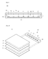
- FIG. 10 is an exploded perspective view showing a display device according to the seventh embodiment.
- the display device 70 includes a board 83, a light emitting module 80 including light emitting devices 10 and 11, a reflective plate 71, a light guide plate 72, an optical sheet 73, and a display panel 74.
- the light emitting module 80, the reflective plate 71, the light guide plate 72, and the optical sheet 73 may serve as a light unit.
- the light unit can be protected by a bottom cover or a bottom chassis.
- the light emitting module 80 includes the light emitting devices 10 and 11 representing the difference of the peak wavelength within 2.5nm. At least one of the light emitting devices 10 and 11 has the wavelength combination as described above.
- the light guide plate 72 is disposed at one side of the light emitting module 80, the reflective plate 71 is disposed below the light guide plate 72 and the optical sheet 73 is disposed above the light guide plate 72.
- the light guide plate 72 may be spaced apart from the light emitting devices 10 and 11 by a distance of 0.5mm or less.
- the light guide plate 72 is made from a PC material or a PMMA (poly methyl methacrylate) material, but the embodiment is not limited thereto.
- the reflective plate 71 reflects the light leaked from the light guide plate 72, and the optical sheet diffuses or collects the light incident through the light guide plate 72 such that the light can be irradiated to the display panel.
- the light emitted from the light emitting module 80 is incident into the light guide plate 72 and the light guide plate 72 guides the light incident from the light emitting module 80 over the whole area of the display device so that the surface light is emitted.
- the optical sheet 73 is disposed above the light guide plate 72.
- the light guide plate 72 and the optical sheet 73 may be defined as an optical member.
- the optical sheet 73 may include at least one of the diffusion sheet, the horizontal/vertical prism sheet, and the brightness enhancement film.
- the display panel 74 may be prepared as an LCD panel.
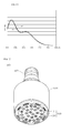
- FIG. 11 is a graph showing spectrums of a plurality of light emitting devices in a light unit according to the embodiment.
- the spectrums shown in the graph are obtained from two light emitting devices and represent wavelengths of green and red phosphors excited by the light emitted from the blue light emitting diode.
- the spectrums P1 and P2 of the two light emitting devices represent the main peaks of the green and red phosphors exited by the light emitted from the blue light emitting device. If the difference of the spectrum peak between two light emitting devices is within 2.5nm, the difference of the intensity of the main peak between the green color and the red color may rarely occur in the spectrums P1 and P2. That is, according to the embodiment, the difference of the peak between the light emitting diodes is set within the critical range in the light emitting device array, so that the difference of the excited wavelength of the phosphor, which is excited by absorbing the light emitted from the light emitting diode, can be reduced.
- the difference of the excited wavelength caused by the light emitting diodes and the phosphor can be reduced, so that the variation of the color sensitivity, such as the reddish or the color stain caused by the difference of the main peaks, can be reduced in the light unit.
- the embodiment can reduce the difference of the color sensitivity between light emitting diodes.
- the embodiment can reduce the difference of the color sensitivity in the set caused by the light emitting device array, so that the color stain or the abnormal color can be reduced.
- the embodiment can provide the light unit having the uniform color distribution.
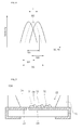
- FIG. 12 is a perspective view showing a lighting device according to the embodiment.
- the lighting device 1500 includes a case 1510, a light emitting module 1530 disposed in the case 1510, and a connection terminal 1520 disposed in the case 1510 to receive power from an external power source.
- the case 1510 includes a material having superior heat dissipation property.
- the case 1510 includes a metallic material or a resin material.
- the light emitting module 1530 may include a board 1532 and light emitting devices 10 and 11 according to the embodiment disposed on the board 1532.
- the light emitting devices 10 and 11 according to the embodiment have main peaks which are different from each other in the same color band.
- the light emitting devices 10 and 11 are spaced apart from each other or arranged in the form of a matrix.
- the board 1532 includes an insulating member printed with a circuit pattern.
- the board 1532 includes a PCB, an MCPCB, an FPCB, a ceramic PCB, and an FR-4 substrate.
- the board 1532 may include a material that effectively reflects the light.
- a coating layer can be formed on the surface of the board 1532. At this time, the coating layer has a white color or a silver color to effectively reflect the light.
- At least one light emitting device can be disposed on the board 1532.
- Each light emitting device 10 or 11 may include at least one LED (light emitting diode) chip.
- the LED chip may include an LED that emits the light of visible ray band having red, green, blue or white color and a UV (ultraviolet) LED that emits UV light.
- the light emitting devices 10 and 11 of the light emitting module 1530 can be variously combined to provide various color sensitivity and brightness.
- the white LED, the red LED and the green LED can be combined to achieve the high color rendering index (CRI).
- connection terminal 1520 is electrically connected to the light emitting module 1530 to supply power to the light emitting module 1530.
- the connection terminal 1520 has a shape of a socket screw-coupled with the external power source, but the embodiment is not limited thereto.
- the connection terminal 1520 can be prepared in the form of a pin inserted into the external power source or connected to the external power source through a wire.
- the light emitting device can emit lights having various colors, so the light emitting device can be used as a light source in various products such as a lighting indicator, a character indicator, and an image display.
- the lighting device may include a lighting lamp, a signal lamp, a headlight of a vehicle, and an electric signboard.
- any reference in this specification to "one embodiment,” “an embodiment,” “example embodiment,” etc. means that a particular feature, structure, or characteristic described in connection with the embodiment is included in at least one embodiment of the invention.
- the appearances of such phrases in various places in the specification are not necessarily all referring to the same embodiment.
Landscapes
- Engineering & Computer Science (AREA)
- Power Engineering (AREA)
- Microelectronics & Electronic Packaging (AREA)
- Physics & Mathematics (AREA)
- Condensed Matter Physics & Semiconductors (AREA)
- General Physics & Mathematics (AREA)
- Computer Hardware Design (AREA)
- Led Device Packages (AREA)
- Non-Portable Lighting Devices Or Systems Thereof (AREA)
Abstract
The light emitting device includes a body (20); a first light emitting diode (31) for emitting a light having a first main peak in a wavelength range of a first color; a second light emitting diode (32) for emitting a light having a second main peak in the wavelength range of the first color; and a plurality of lead electrodes (23,24) electrically connected to at least one of the first and second light emitting diodes on the body. The first main peak of the first light emitting diode and the second main peak of the second light emitting diode have a wavelength difference of at least 75% based on the wavelength range of the first color.
Description
- The embodiment relates to a light emitting device and a light unit having the same.
- A light emitting diode (LED) may constitute a light source for generating light by using GaAs, AlGaAs, GaN, InGaN, and InGaAlP-based compound semiconductor materials.
- Such an LED is packaged so as to be used as a light emitting device that emits lights having various colors. The light emitting device is used as a light source in various products such as a lighting indicator, a character indicator, and an image display.
- The embodiment provides a light emitting device having at least two light emitting diodes.
- The embodiment provides a light emitting device including light emitting diodes capable of emitting lights having the same color band and different main peaks.
- The embodiment provides a light unit including a plurality of light emitting device employing light emitting diodes capable of emitting lights having wavelength bands with different main peaks.
- A light emitting device according to the embodiment includes a body; a first light emitting diode for emitting a light having a first main peak in a wavelength range of a first color; a second light emitting diode for emitting a light having a second main peak in the wavelength range of the first color; and a plurality of lead electrodes electrically connected to at least one of the first and second light emitting diodes on the body, wherein the first main peak of the first light emitting diode and the second main peak of the second light emitting diode have a wavelength difference of at least 75% based on the wavelength range of the first color.
- A light emitting device according to the embodiment includes a body having a cavity; a first light emitting diode for emitting a light having a first main peak in a wavelength range of a first color band; a second light emitting diode for emitting a light having a second main peak in the wavelength range of the first color band; a plurality of lead electrodes electrically connected to at least one of the first and second light emitting diodes on the body; and a resin member disposed in the cavity, wherein a central peak of the first main peak of the first light emitting diode is closer to a short wavelength than to a central wavelength of the first color band, and a central peak of the second main peak of the second light emitting diode is closer to a long wavelength than to the central wavelength of the first color band.
- A light unit according to the embodiment includes a board; and a plurality of light emitting devices arrayed on the board, wherein at least one first light emitting device of the light emitting devices includes a body; a first light emitting diode for emitting a light having a first main peak in a wavelength range of a first color; a second light emitting diode for emitting a light having a second main peak in the wavelength range of the first color; and a plurality of lead electrodes electrically connected to at least one of the first and second light emitting diodes on the body, and wherein the first main peak of the first light emitting diode and the second main peak of the second light emitting diode have a wavelength difference of at least 75% based on the wavelength range of the first color.
-
FIG. 1 is a side sectional view showing a light emitting device according to the first embodiment; -
FIG. 2 is a plan view ofFIG. 1 ; -
FIG. 3 is a table showing an example of mixing of main peaks between light emitting devices according to the embodiment; -
FIG. 4 is a grapy showing an example of mixing of main peaks between light emitting devices shown inFIG. 1 ; -
FIG. 5 is a side sectional view showing a light emitting device package according to the second embodiment; -
FIG. 6 is a side sectional view showing a light emitting device package according to the third embodiment; -
FIG. 7 is a view showing a light emitting module according to the fourth embodiment; -
FIG. 8 is a view showing a light emitting module according to the fifth embodiment; -
FIG. 9 is a side sectional view showing a display device according to the sixth embodiment; -
FIG. 10 is an exploded perspective view showing a display device according to the seventh embodiment; -
FIG. 11 is a graph showing spectrums of a plurality of light emitting devices in a light unit according to the embodiment; and -
FIG. 12 is a perspective view showing a lighting unit including a light emitting device according to the embodiment. - In the description of the embodiments, it will be understood that, when a layer (or film), a region, a pattern, or a structure is referred to as being "on" or "under" another substrate, another layer (or film), another region, another pad, or another pattern, it can be "directly" or "indirectly" on the other substrate, layer (or film), region, pad, or pattern, or one or more intervening layers may also be present. Such a position of the layer has been described with reference to the drawings.
- The thickness and size of each layer shown in the drawings may be exaggerated, omitted or schematically drawn for the purpose of convenience or clarity. In addition, the size of elements does not utterly reflect an actual size.
-
FIG. 1 is a side sectional view showing a light emitting device according to the first embodiment, andFIG. 2 is a plan view ofFIG. 1 ; - Referring to
FIGS. 1 and 2 , alight emitting device 10 includes abody 20 having acavity 22 with an opened top surface, a plurality oflead electrodes light emitting diodes lead electrodes resin member 35 filled in thecavity 22. - The
body 20 may include one of a silicon material, a ceramic material and a resin material. For instance, thebody 20 may include at least one of silicon, silicon carbide (SiC), aluminum nitride (A1N), polyphthalamide (PPA), and liquid crystal polymer (LCP), but the embodiment is not limited thereto. In addition, thebody 20 can be prepared or injection-molded as a structure of a single-layer substrate or a multi-layer substrate, but the embodiment does not limit the shape and the structure of the body. - The
body 20 is formed at an upper portion thereof with thecavity 22 having the opening. Thecavity 22 has a predetermined depth from the top surface of thebody 20. Thecavity 22 may have a concave cup shape or a concave tube shape having a predetermined curvature. In addition, a top surface of thecavity 22 may have a circular shape or a polygonal shape, but the embodiment is not limited thereto. - An inner wall of the
cavity 22 may be inclined toward a bottom surface of thecavity 22 to reflect the incident light toward the opening. - The
lead electrodes body 20. Thelead electrodes body 20 to serve as external electrodes. - The
lead electrodes type lead electrodes - Referring to
FIGS. 1 and 2 , thelight emitting diodes second lead electrode 24 by an adhesive and electrically connected to thelead electrodes wires 34. Thelight emitting diodes - The
light emitting diodes lead electrodes light emitting diodes - In addition, the
light emitting diodes light emitting diodes light emitting device 10 can be changed and thelight emitting diodes - The
resin member 35 is filled in thecavity 22. Theresin member 35 may include a transparent resin material, such as silicon or epoxy. In addition, a top surface of theresin member 35 may have a flat surface, a concave surface or a convex surface and a lens can be attached onto theresin member 35. - At least one type of phosphors can be added to the
resin member 35. The phosphor may include a yellow phosphor or a yellow/red phosphor. For the purpose of convenience of explanation, the following description will be made on the assumption that thelight emitting diodes - The light emitting device according to the embodiment may include a protective device for protecting the
light emitting diodes - The
light emitting diodes light emitting diodes light emitting diodes light emitting diodes light emitting diodes - The
light emitting device 10 includes a plurality oflight emitting diodes light emitting diodes light emitting diode 31 represents the first main peak which is closer to the short wavelength than to the central wavelength of the first color band, and thelight emitting diode 32 represents the second main peak which is closer to the long wavelength than to the central wavelength of the first color band. Hereinafter, the light emitting diode that emits the wavelength spectrum of blue light will be described as an example. The wavelength band of the blue light is about 380nm to about 500nm, preferably, about 380nm to about 480nm, more preferably, about 440nm to about 460nm. The short wavelength of the blue wavelength is about 380nm or less, preferably, about 440nm or less. The long wavelength of the blue wavelength is about 500nm or above, preferably, about 480nm or above, more preferably, about 460nm or above. - The difference in wavelength between the first main peak of the first
light emitting diode 31 and the second main peak of the second light emitting diode is about 75% or more within the wavelength range of one color. The difference in wavelength between the first main peak of the firstlight emitting diode 31 and the second main peak of the second light emitting diode can be represented as the difference between the central peak of the first main peak and the central peak of the second main peak. In addition, the difference in wavelength between the first main peak of the firstlight emitting diode 31 and the second main peak of the second light emitting diode can be represented as the actual wavelength difference, which is obtained by subtracting the second main peak from the first main peak. - When the wavelength range of the blue light is about 440nm to about 460nm, the difference is about 75% or above of 20nm, which is obtained by subtracting 440nm from 460nm, that is, about 15nm or above. For instance, if the wavelength range of the green light is about 525nm to about 535nm, the difference of 75% is about 7.5nm or above. The wavelength range of the red light is about 615nm to about 630nm, so the difference of 75% is about 11.25nm or above. The wavelength range of the yellow light is about 510nm to about 525nm, so the difference of 75% is about 11.25nm or above.
- The main peak may include the dominant wavelength or the FWHM (full width at half maximum).
-
FIG. 3 is a table showing an example of mixing of main peaks between light emitting devices according to the embodiment. - Referring to
FIG. 3 , in the spectrum of the light emitting diode, the blue wavelength band is in the range of about 440nm to about 460nm. For instance, the main peak of the blue wavelength can be obtained in the range of W1 to W8. Each main peak in W1 to W8 can be obtained at an interval of about 0.5nm to about 3.5nm, but the embodiment is not limited thereto. If each main peak is obtained at the interval of 2.5nm in the wavelength spectrum, W1 is about 440nm to about 442.5nm, W2 is about 442.5nm to about 445nm, W3 is about 445nm to about 447.5nm, W4 is about 447.5nm to about 450nm, W5 is about 450nm to about 452.5nm, W6 is about 452,5nm to about 455nm, W7 is about 455nm to about 457.5nm, and W8 is about 457.5nm to about 460nm. - The peak wavelengths of two light emitting diodes can be mixed with each other in the form of M1 to M8 by using A1 to A8 and A2 to H2. The embodiment may include two light emitting diodes (for instance, M1 and M8) representing great difference of the main peak.
- The first and second
light emitting diodes light emitting diodes - According to the embodiment, as shown in
FIG. 4 , for instance, the main peaks of the first and second light emitting diodes having the range of W1 and W8 are mixed so that the main peak Wx having the central peak W0 is represented. The central peak W0 is a peak in a set. For instance, when the central peak W0 is 450nm, the central peak W0 is in the range of 450nm±1.25nm. The first main peak W1 of the first light emitting diode is a short wavelength spaced apart from the central peak (for instance, 450nm) by 37.5% or more, and the second main peak W8 of the second light emitting diode is a long wavelength spaced apart from the central peak (for instance, 450nm) by 37.5% or more. Since 37.5% is 7.5nm, the first and second main peaks W1 and W8 are spaced apart from the central peak W0 by 7.5nm, respectively. That is, in the wavelength range spaced apart from the central peak by 75%, the first main peak W1 of the first light emitting diode is in the range of about 440nm to about 442.5nm and the second main peak W8 of the second light emitting diode is in the range of about 457.5nm to about 460nm. - The difference T between the first main peak W1 of the first light emitting diode and the second main peak W8 of the second light emitting diode corresponds to the difference between the central peak of the first main peak and the central peak of the second main peak. The difference T between the central peaks of the first and second main peaks W1 and W8 is about 75% based on the wavelength range WR of the first color band. In detail, the central peaks of the first and second main peaks W1 and W8 are spaced apart from the central peak W0 of the first color band by about 37.5% in opposition to each other.
- The first main peak W1 of the first light emitting diode can be mixed with the second main peak W8 of the second light emitting diode in such a manner that the main peak Wx can be represented as the central peak in the set. The central peak may be a peak wavelength Wp or the actual central wavelength of the main peak.
- In addition, according to the second embodiment, at least three light emitting
diodes light emitting device 10A as shown inFIG. 5 . Thelight emitting diodes light emitting diodes light emitting diode 33 having a peak wavelength between main peaks of the first and secondlight emitting diodes light emitting device 10A, the firstlight emitting diode 31 is disposed at one side of thecavity 22, the secondlight emitting diode 32 is disposed at the other side of thecavity 22, and the thirdlight emitting diode 33 is disposed at the center of thecavity 22. For instance, the first and secondlight emitting diodes light emitting diode 33 has the third main peak, which is equal or approximate to the average of the central peaks of the first and secondlight emitting diodes - The first to third
light emitting diodes 31 to 33 may be prepared as the combination of W1/W8/W4 or W1/W8/W5 in the table shown inFIG. 3 . In thelight emitting device 10A, the first to thirdlight emitting diodes 31 to 33 may be variously arranged such that they represent the peak wavelength approximate to the central peak of a desired color band. The central peak is the peak wavelength of each color spectrum. For instance, if the peak wavelength is 450nm, the central peak is in the range of 450±1.25nm. - In addition to the light emitting diodes representing the blue wavelength spectrum, at least two light emitting diodes representing the green wavelength spectrum or the red wavelength spectrum can be mixed as described above.
-
FIG. 6 is a side sectional view showing a light emitting device according to the third embodiment. Referring toFIG. 6 , thelight emitting device 10B includes an insulatinglayer 21 formed on a surface of aconductive body 20A, a plurality oflead electrodes conductive body 20A, and a plurality oflight emitting diodes lead electrodes conductive body 20A can be formed by adding N type or P type conductive dopant to a silicon wafer. - According to the third embodiment, a protective device can be formed on the
body 20A to protect thelight emitting diodes light emitting diodes -
FIG. 7 is a view showing a light emitting module according to the fourth embodiment. - Referring to
FIG. 7 , thelight emitting module 60 includes firstlight emitting devices 10 according to the first embodiment and secondlight emitting devices 11 having wavelength combination different from that of the firstlight emitting devices 10. The first and secondlight emitting devices board 63. Theboard 63 may selectively include a substrate having a metal plate, a resin PCB, a ceramic substrate or a flexible substrate. - In detail, the first and second
light emitting devices board 63. - The structure of the first
light emitting device 10 has been described with reference toFIG. 1 , and the secondlight emitting device 11 may include at least one of M2 to M7 shown in the table ofFIG. 3 . According to the embodiment, the number of light emitting diodes disposed in the firstlight emitting device 10 may be different from the number of light emitting diodes disposed in the secondlight emitting device 11, but the embodiment is not limited thereto. In addition, according to the embodiment, only thelight emitting devices 10 shown inFIG. 1 can be arrayed on theboard 63. Further, according to the embodiment, the light emitting devices shown inFIG. 5 or6 can be selectively used in addition to the light emitting devices shown inFIG. 1 . - The
light emitting module 60 shown inFIG. 7 includes a plurality of light emittingdevices devices - In addition, as shown in
FIG. 8 , alight emitting module 60A may include firstlight emitting devices 10 having wavelength combination as shown inFIG. 1 and light emittingdevices light emitting devices 10. For instance, thelight emitting devices FIG. 3 . - The
light emitting module 60A shown inFIG. 8 includes a plurality of light emittingdevices light emitting devices - According to the fifth embodiment, as shown in
FIGS. 7 and 8 , the difference of the central peak between two different light emitting devices in thelight emitting module -
FIG. 9 is a sectional view showing a display device according to the sixth embodiment. - Referring to
FIG. 9 , thedisplay device 50 includes abottom cover 52, a plurality of light emittingdevices board 63, anoptical sheet 54 and adisplay panel 55. Theboard 63, thebottom cover 52, and theoptical sheet 54 may serve as alight unit 51. - The
bottom cover 52 includes arecess 53 having an open top surface. An inner wall of the recess is inclined. Thebottom cover 52 and a lateral side of thebottom cover 52 may be prepared as separate structures, but the embodiment is not limited thereto. - At least one
board 63 is disposed on thebottom cover 52. The first and secondlight emitting devices board 63. According to the embodiment, the first and secondlight emitting devices board 63 such that the difference of the central peak between the first and secondlight emitting devices devices light emitting devices - The
optical sheet 54 may include at least one of a diffusion sheet, a horizontal/vertical prism sheet and a brightness enhancement sheet. The diffusion sheet diffuses the incident light, the horizontal/vertical prism sheet concentrates the incident light onto the display region, and the brightness enhancement sheet improves the light efficiency by reusing the wasted light. - For instance, the
display panel 55 may be an LCD panel including first and second substrates and a liquid crystal layer interposed between the first and second substrates. The first substrate may include a color filter array substrate and the second substrate may include a TFT array substrate, or vice versa. However, the embodiment is not limited to the above display panel, but various modifications are possible. A polarizing plate can be attached to at least one surface of the display panel, but the embodiment is not limited thereto. -
FIG. 10 is an exploded perspective view showing a display device according to the seventh embodiment. - Referring to
FIG. 10 , thedisplay device 70 includes aboard 83, alight emitting module 80 including light emittingdevices reflective plate 71, alight guide plate 72, anoptical sheet 73, and adisplay panel 74. Thelight emitting module 80, thereflective plate 71, thelight guide plate 72, and theoptical sheet 73 may serve as a light unit. The light unit can be protected by a bottom cover or a bottom chassis. - The
light emitting module 80 includes thelight emitting devices light emitting devices - The
light guide plate 72 is disposed at one side of thelight emitting module 80, thereflective plate 71 is disposed below thelight guide plate 72 and theoptical sheet 73 is disposed above thelight guide plate 72. Thelight guide plate 72 may be spaced apart from thelight emitting devices light guide plate 72 is made from a PC material or a PMMA (poly methyl methacrylate) material, but the embodiment is not limited thereto. - The
reflective plate 71 reflects the light leaked from thelight guide plate 72, and the optical sheet diffuses or collects the light incident through thelight guide plate 72 such that the light can be irradiated to the display panel. - The light emitted from the
light emitting module 80 is incident into thelight guide plate 72 and thelight guide plate 72 guides the light incident from thelight emitting module 80 over the whole area of the display device so that the surface light is emitted. Theoptical sheet 73 is disposed above thelight guide plate 72. Thelight guide plate 72 and theoptical sheet 73 may be defined as an optical member. - The
optical sheet 73 may include at least one of the diffusion sheet, the horizontal/vertical prism sheet, and the brightness enhancement film. For instance, thedisplay panel 74 may be prepared as an LCD panel. -
FIG. 11 is a graph showing spectrums of a plurality of light emitting devices in a light unit according to the embodiment. The spectrums shown in the graph are obtained from two light emitting devices and represent wavelengths of green and red phosphors excited by the light emitted from the blue light emitting diode. - As shown in
FIG. 11 , the spectrums P1 and P2 of the two light emitting devices represent the main peaks of the green and red phosphors exited by the light emitted from the blue light emitting device. If the difference of the spectrum peak between two light emitting devices is within 2.5nm, the difference of the intensity of the main peak between the green color and the red color may rarely occur in the spectrums P1 and P2. That is, according to the embodiment, the difference of the peak between the light emitting diodes is set within the critical range in the light emitting device array, so that the difference of the excited wavelength of the phosphor, which is excited by absorbing the light emitted from the light emitting diode, can be reduced. In detail, the difference of the excited wavelength caused by the light emitting diodes and the phosphor can be reduced, so that the variation of the color sensitivity, such as the reddish or the color stain caused by the difference of the main peaks, can be reduced in the light unit. - The embodiment can reduce the difference of the color sensitivity between light emitting diodes. The embodiment can reduce the difference of the color sensitivity in the set caused by the light emitting device array, so that the color stain or the abnormal color can be reduced. The embodiment can provide the light unit having the uniform color distribution.
-
FIG. 12 is a perspective view showing a lighting device according to the embodiment. - Referring to
FIG. 12 , thelighting device 1500 includes acase 1510, alight emitting module 1530 disposed in thecase 1510, and aconnection terminal 1520 disposed in thecase 1510 to receive power from an external power source. - Preferably, the
case 1510 includes a material having superior heat dissipation property. For instance, thecase 1510 includes a metallic material or a resin material. - The
light emitting module 1530 may include aboard 1532 and light emittingdevices board 1532. Thelight emitting devices light emitting devices - The
board 1532 includes an insulating member printed with a circuit pattern. For instance, theboard 1532 includes a PCB, an MCPCB, an FPCB, a ceramic PCB, and an FR-4 substrate. - In addition, the
board 1532 may include a material that effectively reflects the light. A coating layer can be formed on the surface of theboard 1532. At this time, the coating layer has a white color or a silver color to effectively reflect the light. - At least one light emitting device can be disposed on the
board 1532. Eachlight emitting device - The
light emitting devices light emitting module 1530 can be variously combined to provide various color sensitivity and brightness. For instance, the white LED, the red LED and the green LED can be combined to achieve the high color rendering index (CRI). - The
connection terminal 1520 is electrically connected to thelight emitting module 1530 to supply power to thelight emitting module 1530. Theconnection terminal 1520 has a shape of a socket screw-coupled with the external power source, but the embodiment is not limited thereto. For instance, theconnection terminal 1520 can be prepared in the form of a pin inserted into the external power source or connected to the external power source through a wire. - The light emitting device according to the embodiment can emit lights having various colors, so the light emitting device can be used as a light source in various products such as a lighting indicator, a character indicator, and an image display. In addition, the lighting device may include a lighting lamp, a signal lamp, a headlight of a vehicle, and an electric signboard.
- Any reference in this specification to "one embodiment," "an embodiment," "example embodiment," etc., means that a particular feature, structure, or characteristic described in connection with the embodiment is included in at least one embodiment of the invention. The appearances of such phrases in various places in the specification are not necessarily all referring to the same embodiment. Further, when a particular feature, structure, or characteristic is described in connection with any embodiment, it is submitted that it is within the purview of one skilled in the art to effect such feature, structure, or characteristic in connection with other ones of the embodiments.
- Although embodiments have been described with reference to a number of illustrative embodiments thereof, it should be understood that numerous other modifications and embodiments can be devised by those skilled in the art that will fall within the spirit and scope of the principles of this disclosure. More particularly, various variations and modifications are possible in the component parts and/or arrangements of the subject combination arrangement within the scope of the disclosure, the drawings and the appended claims. In addition to variations and modifications in the component parts and/or arrangements, alternative uses will also be apparent to those skilled in the art.
Claims (14)
- A light emitting device comprising:a body (20);a first light emitting diode (31) for emitting a light having a first main peak in a wavelength range of a first color band;a second light emitting diode (32) for emitting a light having a second main peak in the wavelength range of the first color band; anda plurality of lead electrodes (23,24) electrically connected to at least one of the first and second light emitting diodes on the body,wherein a difference of a central peak between the first main peak of the first light emitting diode (31) and the second main peak of the second light emitting diode (32) is at least 75% based on the wavelength range of the first color band.
- The light emitting device of claim 1, wherein difference of the central peak between the first main peak of the first light emitting diode (31) and the second main peak of the second light emitting diode (32) is at least 15nm based on the wavelength range of the first color.
- The light emitting device of claim 1 , wherein the first main peak of the first light emitting diode (31) is shifted from a central wavelength of the first color band in a short wavelength direction by at least 7.5nm.
- The light emitting device of claim 3, wherein the second main peak of the second light emitting diode (32) is shifted from a central wavelength of the first color band in a long wavelength direction by at least 7.5nm.
- The light emitting device of any one of claims 1 to 4, further comprising a cavity (22) formed at an upper portion of the body, wherein the first and second light emitting diodes (31, 32) and the lead electrodes (23,24) are disposed in the cavity, further comprising a resin member (35) filled in the cavity (22).
- The light emitting device of claim 5, wherein the resin member (35) includes at least one of a green phosphor, a yellow phosphor, and a red phosphor.
- The light emitting device of claim 4, further comprising a third light emitting diode (33) disposed between the first and second light emitting diodes (31, 32).
- The light emitting device of claim 7, wherein a central peak of a third main peak of a light emitted from the third light emitting diode has a difference within 2.5nm with respect to an average of central peaks of the first and second main peaks.
- The light emitting device of any one of claims 1 to 5 , wherein the first and second light emitting diodes (31,32) emit a blue light.
- The light emitting device of claim 9, wherein the first and second light emitting diodes (31, 32) emit lights having a wavelength in a range of 440nm to 460nm.
- The light emitting device of claim 4, wherein the long wavelength is equal to or lower than 440nm, and the long wavelength is equal to or higher than 460nm.
- The light emitting device of claim 9, wherein the first main peak of the first light emitting diode (31) is in a range of 440nm to 442.5nm and the second main peak of the second light emitting diode (32) is in a range of 457.5nm to 460nm.
- The light emitting device of claim 9, wherein a central peak of the first main peak of the first light emitting diode (31) is closer to a short wavelength than to a central wavelength of the first color band, and a central peak of the second main peak of the second light emitting diode (32) is closer to a long wavelength than to the central wavelength of the first color band.
- A light unit comprising:a board(63); anda plurality of light emitting devices (10, 11) arrayed on the board (63),wherein at least one (10, 11) of the light emitting devices is any one of claims 1-14,wherein the difference of the central peak between the first main peak of the first light emitting diode and the second main peak of the second light emitting diode is at least 15nm.
Applications Claiming Priority (1)
| Application Number | Priority Date | Filing Date | Title |
|---|---|---|---|
| KR1020100027405A KR100999809B1 (en) | 2010-03-26 | 2010-03-26 | Light emitting device and light unit having thereof |
Publications (1)
| Publication Number | Publication Date |
|---|---|
| EP2369623A2 true EP2369623A2 (en) | 2011-09-28 |
Family
ID=43512616
Family Applications (1)
| Application Number | Title | Priority Date | Filing Date |
|---|---|---|---|
| EP11159496A Withdrawn EP2369623A2 (en) | 2010-03-26 | 2011-03-24 | Light emitting device having several light emitting diodes and light unit having the same |
Country Status (6)
| Country | Link |
|---|---|
| US (1) | US8132934B2 (en) |
| EP (1) | EP2369623A2 (en) |
| JP (1) | JP2011211196A (en) |
| KR (1) | KR100999809B1 (en) |
| CN (1) | CN102201504A (en) |
| TW (1) | TW201203504A (en) |
Families Citing this family (15)
| Publication number | Priority date | Publication date | Assignee | Title |
|---|---|---|---|---|
| KR20130014256A (en) * | 2011-07-29 | 2013-02-07 | 엘지이노텍 주식회사 | Light emitting device package and lighting system using the same |
| JP2013135083A (en) * | 2011-12-26 | 2013-07-08 | Toyoda Gosei Co Ltd | Light-emitting device |
| JP5781631B2 (en) * | 2012-01-31 | 2015-09-24 | シャープ株式会社 | LED classification method, LED classification apparatus, LED classification program, and recording medium |
| US8757839B2 (en) | 2012-04-13 | 2014-06-24 | Cree, Inc. | Gas cooled LED lamp |
| US9410687B2 (en) | 2012-04-13 | 2016-08-09 | Cree, Inc. | LED lamp with filament style LED assembly |
| US9395051B2 (en) * | 2012-04-13 | 2016-07-19 | Cree, Inc. | Gas cooled LED lamp |
| JP2014007355A (en) * | 2012-06-27 | 2014-01-16 | Rohm Co Ltd | Semiconductor light-emitting device and lighting device |
| CN103545300B (en) * | 2012-07-09 | 2016-07-06 | 展晶科技(深圳)有限公司 | Package structure for LED |
| JP2014096505A (en) * | 2012-11-09 | 2014-05-22 | Sharp Corp | Backlight and method for manufacturing the same |
| TWI523277B (en) * | 2013-07-12 | 2016-02-21 | White light emitting diode module with ultraviolet light | |
| JP2015046445A (en) * | 2013-08-27 | 2015-03-12 | 富士通株式会社 | Compound semiconductor device and method of manufacturing the same |
| CN106322225B (en) * | 2015-06-16 | 2019-05-10 | 群创光电股份有限公司 | The backlight of display device |
| US9825206B2 (en) * | 2016-02-25 | 2017-11-21 | Toyoda Gosei, Co., Ltd. | Light-emitting device |
| TWI646651B (en) * | 2017-01-26 | 2019-01-01 | 宏碁股份有限公司 | Light-emitting diode display and manufacturing method thereof |
| TWI741799B (en) * | 2020-09-18 | 2021-10-01 | 葳天科技股份有限公司 | Light-emitting apparatus |
Family Cites Families (12)
| Publication number | Priority date | Publication date | Assignee | Title |
|---|---|---|---|---|
| JP4932078B2 (en) * | 2000-12-04 | 2012-05-16 | 日亜化学工業株式会社 | Light emitting device and manufacturing method thereof |
| JP3840940B2 (en) * | 2001-09-28 | 2006-11-01 | 株式会社日立製作所 | Image display device |
| US7066623B2 (en) * | 2003-12-19 | 2006-06-27 | Soo Ghee Lee | Method and apparatus for producing untainted white light using off-white light emitting diodes |
| KR100655894B1 (en) * | 2004-05-06 | 2006-12-08 | 서울옵토디바이스주식회사 | Light Emitting Device |
| JP4534717B2 (en) * | 2004-10-29 | 2010-09-01 | 豊田合成株式会社 | Light emitting device |
| KR20060061867A (en) * | 2004-12-02 | 2006-06-08 | 삼성전자주식회사 | Light generating device and display device having the same |
| JP2006352030A (en) | 2005-06-20 | 2006-12-28 | Arumo Technos Kk | Light emitting diode |
| JP4989936B2 (en) * | 2006-07-27 | 2012-08-01 | 株式会社朝日ラバー | Lighting device |
| KR100862446B1 (en) | 2007-01-26 | 2008-10-08 | 삼성전기주식회사 | White light led light source module |
| JP5346448B2 (en) | 2007-06-07 | 2013-11-20 | シャープ株式会社 | LIGHT EMITTING DEVICE AND CAMERA MOBILE MOBILE WITH THE SAME |
| KR100891810B1 (en) | 2007-11-06 | 2009-04-07 | 삼성전기주식회사 | White light emitting device |
| CN101482235B (en) * | 2009-01-22 | 2012-05-30 | 深圳市聚飞光电股份有限公司 | Color temperature-adjustable high-color development LED lamp and manufacturing method thereof |
-
2010
- 2010-03-26 KR KR1020100027405A patent/KR100999809B1/en active IP Right Grant
-
2011
- 2011-03-23 TW TW100109827A patent/TW201203504A/en unknown
- 2011-03-24 US US13/070,616 patent/US8132934B2/en not_active Expired - Fee Related
- 2011-03-24 EP EP11159496A patent/EP2369623A2/en not_active Withdrawn
- 2011-03-24 JP JP2011065438A patent/JP2011211196A/en active Pending
- 2011-03-28 CN CN2011100788270A patent/CN102201504A/en active Pending
Non-Patent Citations (1)
| Title |
|---|
| None |
Also Published As
| Publication number | Publication date |
|---|---|
| KR100999809B1 (en) | 2010-12-08 |
| CN102201504A (en) | 2011-09-28 |
| US20110235363A1 (en) | 2011-09-29 |
| TW201203504A (en) | 2012-01-16 |
| JP2011211196A (en) | 2011-10-20 |
| US8132934B2 (en) | 2012-03-13 |
Similar Documents
| Publication | Publication Date | Title |
|---|---|---|
| US8132934B2 (en) | Light emitting device and light unit having the same | |
| US10541235B2 (en) | Light emitting device package | |
| US10677417B2 (en) | Package for light emitting device and method for packaging the same | |
| US8309983B2 (en) | Light emitting device package and lighting system having the same | |
| US8278670B2 (en) | Light emitting apparatus and display apparatus having the same | |
| KR100901618B1 (en) | Light emitting diode package and manufacturing method thereof | |
| JP6299176B2 (en) | LIGHT EMITTING DEVICE, ITS MANUFACTURING METHOD, AND LIGHTING DEVICE EQUIPPED WITH THE LIGHT EMITTING DEVICE | |
| EP2551927A1 (en) | Light emitting device package | |
| US8344601B2 (en) | Light emitting device | |
| KR20120132931A (en) | Light-emitting device | |
| EP2346103A2 (en) | Light emitting device and backlight unit | |
| EP2445020B1 (en) | Light emitting diode package structure | |
| KR20120045539A (en) | Light emitting device package | |
| KR101683888B1 (en) | Light emitting apparatus and display apparatus having the same | |
| JP5779220B2 (en) | Phosphor and light emitting device including the same | |
| KR20170073350A (en) | Phosphor and light emitting device having thereof | |
| KR20170073353A (en) | Light emitting device and lighting system having thereof | |
| TWI381544B (en) | Method for manufacturing light emitting diode device with multiple wavelengths | |
| KR20120073929A (en) | Light emitting device package | |
| KR20130079869A (en) | Light emitting device package and lighting system including the same |
Legal Events
| Date | Code | Title | Description |
|---|---|---|---|
| PUAI | Public reference made under article 153(3) epc to a published international application that has entered the european phase |
Free format text: ORIGINAL CODE: 0009012 |
|
| 17P | Request for examination filed |
Effective date: 20110415 |
|
| AK | Designated contracting states |
Kind code of ref document: A2 Designated state(s): AL AT BE BG CH CY CZ DE DK EE ES FI FR GB GR HR HU IE IS IT LI LT LU LV MC MK MT NL NO PL PT RO RS SE SI SK SM TR |
|
| AX | Request for extension of the european patent |
Extension state: BA ME |
|
| STAA | Information on the status of an ep patent application or granted ep patent |
Free format text: STATUS: THE APPLICATION IS DEEMED TO BE WITHDRAWN |
|
| 18D | Application deemed to be withdrawn |
Effective date: 20141001 |