EP2367259A2 - Batteriepack und Verfahren zur Ladung eines Batteriepacks - Google Patents
Batteriepack und Verfahren zur Ladung eines Batteriepacks Download PDFInfo
- Publication number
- EP2367259A2 EP2367259A2 EP10197007A EP10197007A EP2367259A2 EP 2367259 A2 EP2367259 A2 EP 2367259A2 EP 10197007 A EP10197007 A EP 10197007A EP 10197007 A EP10197007 A EP 10197007A EP 2367259 A2 EP2367259 A2 EP 2367259A2
- Authority
- EP
- European Patent Office
- Prior art keywords
- voltage
- charging
- battery cell
- battery pack
- switching element
- Prior art date
- Legal status (The legal status is an assumption and is not a legal conclusion. Google has not performed a legal analysis and makes no representation as to the accuracy of the status listed.)
- Withdrawn
Links
Images


Classifications
-
- H—ELECTRICITY
- H02—GENERATION; CONVERSION OR DISTRIBUTION OF ELECTRIC POWER
- H02J—ELECTRIC POWER NETWORKS; CIRCUIT ARRANGEMENTS OR SYSTEMS FOR SUPPLYING OR DISTRIBUTING ELECTRIC POWER; SYSTEMS FOR STORING ELECTRIC ENERGY
- H02J7/00—Circuit arrangements for charging or discharging batteries or for supplying loads from batteries
- H02J7/60—Circuit arrangements for charging or discharging batteries or for supplying loads from batteries including safety or protection arrangements
- H02J7/663—Circuit arrangements for charging or discharging batteries or for supplying loads from batteries including safety or protection arrangements using battery or load disconnect circuits
-
- H—ELECTRICITY
- H01—ELECTRIC ELEMENTS
- H01M—PROCESSES OR MEANS, e.g. BATTERIES, FOR THE DIRECT CONVERSION OF CHEMICAL ENERGY INTO ELECTRICAL ENERGY
- H01M10/00—Secondary cells; Manufacture thereof
- H01M10/42—Methods or arrangements for servicing or maintenance of secondary cells or secondary half-cells
- H01M10/44—Methods for charging or discharging
- H01M10/441—Methods for charging or discharging for several batteries or cells simultaneously or sequentially
-
- Y—GENERAL TAGGING OF NEW TECHNOLOGICAL DEVELOPMENTS; GENERAL TAGGING OF CROSS-SECTIONAL TECHNOLOGIES SPANNING OVER SEVERAL SECTIONS OF THE IPC; TECHNICAL SUBJECTS COVERED BY FORMER USPC CROSS-REFERENCE ART COLLECTIONS [XRACs] AND DIGESTS
- Y02—TECHNOLOGIES OR APPLICATIONS FOR MITIGATION OR ADAPTATION AGAINST CLIMATE CHANGE
- Y02E—REDUCTION OF GREENHOUSE GAS [GHG] EMISSIONS, RELATED TO ENERGY GENERATION, TRANSMISSION OR DISTRIBUTION
- Y02E60/00—Enabling technologies; Technologies with a potential or indirect contribution to GHG emissions mitigation
- Y02E60/10—Energy storage using batteries
Definitions
- the disclosed technology relates to a battery pack and a method of charging the battery pack.
- a battery may take the form of a battery pack which has a battery cell and a protection circuit for controlling charging and discharging of the battery cell, and may be lithium ion batteries, nickel-cadmium (Ni-Cd) batteries, and the like.
- discharging voltage and charging voltage vary according to the type of battery cells.
- charging voltage may vary according to the configuration of bare cells in the battery cells even if the type of battery cells is the same. Battery cells are charged with a rated voltage, or otherwise battery cells may be damaged. Thus, when battery cells are charged, chargers use voltages which correspond to the type of battery cells used.
- aspects include a battery pack that is chargeable by any of a variety of types of chargers and a method of charging the battery pack.
- One aspect is a battery pack including a chargeable battery cell, a charging terminal part selectively connectable to the battery cell, a protection circuit configured to control charging and discharging of the battery cell, and a first switching element connected between the battery cell and the charging terminal part.
- the battery pack also includes a converter circuit connected to the charging terminal part, the converter circuit configured to receive an input voltage applied to the charging terminal part and to output a voltage different from the input voltage, and a second switching element connected between the converter circuit and the battery cell.
- Another aspect is a method of charging a battery pack including a battery cell and a charging control circuit for controlling charging of the battery cell.
- the method includes determining that a charger is connected to the battery pack, determining a first voltage applied by the charger, determining a voltage for charging the battery cell, and charging the battery cell with one of the first voltage and a voltage based on the first voltage according to the voltage for charging the battery cell.
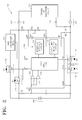
- FIG. 1 is a block diagram illustrating a battery pack 100 according to an embodiment.
- the battery pack 100 includes a battery cell 110, a charging terminal part 120, a protection circuit 130, a first switching element 140, a second switching element 150, a first converter circuit 160, and a charging and discharging switch 170.
- the battery cell 110 may include at least one bare cell. If the battery cell 110 is connected to an external device through the charging terminal part 120, the battery cell 110 may be charged or discharged.
- the bare cell includes an electrode assembly including a positive electrode plate, a negative electrode plate, a separator, a can accommodating the electrode assembly therein and having a top opening, and a cap assembly covering the top opening of the can to seal the can.
- the battery cell 110 may be a rechargeable secondary battery.
- the battery cell 110 may have various output voltages. The voltages that may be output by the battery cell 110 include a common voltage and a high voltage. In some embodiments, the common voltage may be about 4.2 V, and the high voltage may be in the range of about 4.35 V to about 4.4 V.
- the charging terminal part 120 may be connected to an external charger.
- the charging terminal part 120 includes a positive electrode terminal 121 and a negative electrode terminal 122.
- the charging terminal part 120 is connected in parallel to the battery cell 110, and may be connected to an external charger to charge the battery cell 110. If the charging terminal part 120 is connected to an external electronic device, the battery cell 100 is discharged via the charging terminal part 120.
- a path between the charging terminal part 120 and the battery cell 110 may be a large current path used for charging and discharging the battery cell 110.
- a large current may flow via the large current path.
- the protection circuit 130 controls internal operations of the battery pack 100 to allow the battery cell 110 to stably operate.
- the protection circuit 130 controls the first switching element 140, the second switching element 150, and the charging and discharging switch 170 to control the charging and discharging of the battery cell 110.
- the protection circuit 130 detects the voltage output by the battery cell 110 via a VDD terminal, and if the protection circuit 130 determines that the battery cell 110 is overcharged or over-discharged, a charging control signal Sc or a discharging control signal Sd is applied to the charging and discharging switch 170.
- the charging control signal Sc and the discharging control signal Sd may control a transistor included in the charging and discharging switch 170 to selectively interrupt current flow.
- the protection circuit 130 determines an input voltage applied to the charging terminal part 120 and the voltage for charging the battery cell 110.
- the input voltage applied to the charging terminal part 120 may, for example, be an output voltage of a charger.
- the protection circuit 130 outputs a switching control signal Cs via a VT terminal.
- the switching control signal CS controls any one of the first switching element 140 and the second switching element 150 to be in an on-state.
- the input voltage applied to the charging terminal part 120 and the voltage for charging the battery cell 110 may be determined based on a voltage applied to a VR terminal.
- the first switching element 140 is connected between the battery cell 110 and the charging terminal part 120 on the large current path to form a charging or discharging path.
- the first switching element 140 is controlled to be in one of on and off states by the switching control signal CS generated by the protection circuit 130. When the first switching element 140 is in the on-state, a charging voltage from the charger connected to the charging terminal part 120 is applied to the battery cell 110.
- the second switching element 150 is connected between the battery cell 110 and the first converter circuit 160 on a current path to form a charging or discharging path.
- the second switching element 150 is controlled to be in one of on and off states by the switching control signal CS generated by the protection circuit 130. When the second switching element 150 is in an on-state, an output voltage of the first converter circuit 160 is applied to the battery cell 110.
- the first converter circuit 160 increases or decreases the voltage applied to the charging terminal part 120 according to a control signal generated by the protection circuit 130, and outputs the voltage to the second switching element 150.
- the first converter circuit 160 may include a voltage increasing circuit for increasing the voltage applied thereto, and a voltage decreasing circuit for decreasing the voltage applied thereto.
- the voltage applied to the first converter circuit 160 is the output voltage of the charger.
- the output voltage of the charger corresponds to the voltage for charging the battery cell to be charged by the charger.
- the voltage applied to the first converter circuit 160 may be about 4.2 V, and may also be in the range of about 4.3 V to about 4.5 V.
- the charging and discharging switch 170 controls the charging and discharging of the battery cell 110 according to the charging and discharging control signals Sc and Sd applied from the protection circuit 130.
- FIG. 2 is a circuit diagram of the battery pack of FIG. 1 .
- the charging terminal part 120 includes the positive electrode terminal 121 and the negative electrode terminal 122.
- the positive electrode terminal 121 and the negative electrode terminal 122 are connected to an electronic device, the battery cell 110 is discharged.
- the positive electrode terminal 121 and the negative electrode terminal 122 are connected to a charger, the battery cell 110 is charged.
- the negative electrode terminal 122 may be connected to a capacitance detecting resistor R4 that represents the capacitance of the battery cell 110.
- One terminal 123 of the capacitance detecting resistor R4 is connected to an external device, and the external device detects a resistance value of the capacitance detecting resistor R4 to determine the capacitance of the battery cell 110.
- the protection circuit 130 includes a logic circuit 131, a resistance detecting circuit 132, a plurality of overcharging detecting parts 133 and 134, an over-current detecting circuit 135, a plurality of input terminals, and a plurality of output terminals.
- the protection circuit 130 may include VSS, VDD, ID, VR1, VR2 and VR3 terminals as input terminals, and includes VT, VC, DC and CC terminals as output terminals.
- the logic circuit 131 controls the operation of the protection circuit 130, and generally controls the charging and discharging of the battery cell 110.
- the logic circuit 131 generates the switching control signal CS, the charging control signal Sc, the discharging control signal Sd, and a voltage increasing control signal according to the output voltage of the charger, the voltage for charging the battery cell 100, charging and discharging states of the battery cell 110, and internal current flow state of the battery pack 100.
- the switching control signal CS, the charging control signal Sc, the discharging control signal Sd, and the voltage increasing control signal are respectively output via the VT terminal, the DC terminal, the CC terminal, and the VC terminal, respectively.
- the voltage for charging the battery cell 110 may be previously stored in the logic circuit 131.
- the protection circuit 130 may include the resistance detecting circuit 132.
- the resistance detecting circuit 132 recognizes a resistor Ra connected between the VR1 terminal and the VR2 terminal of the protection circuit 130 and a resistor Rb connected between the VR2 terminal and the VR3 terminal of the protection circuit 130.
- a voltage is applied to the resistors Ra and Rb, and the resistance detecting circuit 132 may detect the voltage for charging the battery cell 110 and the output voltage of the charger from voltage values corresponding to resistance values of the resistors Ra and Rb.
- the resistance values of the resistors Ra and Rb may vary according to the voltage for charging the battery cell 110.
- the voltage for charging the battery cell 110 may be determined by using a ratio of the resistance value of the resistor Ra to the resistance value of the resistor Rb.
- the output voltage of the charger may be determined in such a way that the total values of the resistance values of the resistors Ra and Rb remain constant.
- the output voltage of the charger is 4.2 V
- 1.4 V is imposed between the VR1 terminal and the VR2 terminal
- 0.7 V is imposed between the VR2 terminal and the VR3 terminal.
- the resistance detecting circuit 132 detects the voltages of 1.4 V and 0.7 V to determine that the voltage for charging the battery cell 110 is a common voltage.
- 2.1 V is imposed between the VR1 terminal and the VR3 terminal, and the resistance detecting circuit 132 detects the voltage of 2.1 V to determine that the output voltage of the charger is 4.2 V.
- 0.725 V is imposed between the VR1 terminal and the VR2 terminal
- 1.45 V is imposed between the VR2 terminal and the VR3 terminal.
- the resistance detecting circuit 132 detects the voltages of 0.725 V and 1.45 V to determine that the voltage for charging the battery cell 110 is a high voltage.
- 2.175 V is imposed between the VR1 terminal and the VR3 terminal, and the resistance detecting circuit 132 detects the voltage of 2.175 V to determine that the output voltage of the charger is 4.35 V.
- the determination method of the voltage for charging the battery cell 110 and the output voltage of the charger described above is an example and is not limited thereto. That is, the voltage for charging the battery cell 110 and the output voltage of the charger could be determined using other methods.
- the plurality of overcharging detecting parts 133 and 134 compare a voltage applied to the VDD terminal with reference voltages Vref1 and Vref2 to detect whether the battery cell 110 is overcharged.
- the VDD terminal is connected to a terminal between a capacitor C1 and a resistor R1 connected in series between positive and negative electrodes of the battery cell 110.
- the over-current detecting circuit 135 measures a current supplied to the ID terminal to detect whether there is an over-current flowing inside the battery pack 100.
- a resistor R2 may be connected between the ID terminal and the negative electrode terminal 122.
- the protection circuit 130 has a ground terminal that connects the VSS terminal with the negative electrode of the battery cell 110.
- the first switching element 140 includes a field effect transistor (FET) and a parasitic diode (D), and the second switching element 150 includes a FET and a D.
- the first switching element 140 includes a FET1 and a D1
- the second switching element 150 includes a FET2 and a D2.
- a channel type of the FET1 may be different from a channel type of the FET2.
- the FET1 may be an n-channel FET
- the FET2 may be a p-channel FET, or vice versa.
- Both the first switching element 140 and the second switching element 150 form a path for charging.
- source electrodes of the FET1 and the FET2 are connected to the positive electrode of the battery cell 110. Accordingly, when the battery cell 110 is charged, a charging current may be prevented from being supplied to the battery cell 110 simultaneously via the first switching element 140 and the second switching element 150.
- the FET1 of the first switching element 140 and the FET2 of the second switching element 150 are switching devices, and may be any of other kinds of electric devices that may act as a switching device.
- the charging and discharging switch 170 may include a charging control switch 171 and a discharging control switch 172.
- the charging control switch 171 includes a FET3 and a D3
- the discharging control switch 172 includes a FET4 and a D4.
- a connection direction between a source and a drain of the FET3 of the charging control switch 171 are set opposite to those of the transistor FET4 of the discharging control switch 172.
- the FET3 of the charging control switch 171 is connected so as to restrict a current flowing from the charging terminal part 120 towards the battery cell 110
- the FET4 of the discharging control switch 172 is connected so as to restrict a current flowing from the battery cell 110 towards the charging terminal part 120.
- the FET3 of the charging control switch 171 and the FET4 of the discharging control switch 172 are switching devices, and may be any of other kinds of electric devices that may act as a switching device.
- the D3 of the charging control switch 171 and the D4 of the discharging control switch 172 are connected in opposite directions in which current is restricted by FETs thereof.
- FIG. 3 is a flowchart illustrating a method of charging a battery pack, according to an embodiment.
- the battery cell 110 recognizes that the charger is connected to the charging terminal part 120 (operation S100).
- the charger detects an internal resistance value of the battery pack 100 to determine the capacitance of the battery cell 110.
- the battery pack 100 determines the voltage for charging the battery cell 110 and the output voltage of the charger by using the resistance detecting circuit 132 (operations S101 and S102).
- the battery pack 100 may determine whether the voltage for charging the battery cell 110 is a high voltage or a common voltage.
- the battery pack 100 may determine whether the charger is a charger for a common voltage type battery cell or a charger for a high voltage type battery cell.
- the common voltage may indicate that the output of the battery cell 110 is about 4.2 V
- the high voltage may indicate that the output of the battery cell is in the range of about 4.35 V to about 4.4 V.
- the voltage for charging the battery cell 110 may be determined by using resistance values of the resistors connected to the protection circuit 130, but is not limited thereto.
- the voltage for charging the battery cell 110 may be determined by previously storing the voltage for charging the battery cell 110 in the logic circuit 131, when the battery pack 100 is manufactured.
- the output voltage of the charger is substantially the same as a charging voltage (operation S103), and if different, whether the charging voltage is greater than the output voltage of the charger (operation S105).
- the charging voltage is used to charge the battery cell 110, and its value depends on the voltage for charging the battery cell 110.
- the logic circuit 131 applies the low-level switching control signal CS to the first switching element 140 to switch on the FET1 (operation S104).
- the logic circuit 131 applies the high-level charging control signal Sc to the charging control switch 171 to switch on the FET3.
- a large current path through the positive electrode terminal 121, the FET1, the battery cell 110, the D4, the FET3, and the negative electrode terminal 122 is formed.
- the logic circuit 131 controls the first converter circuit 160 to increase the output voltage of the charger and output a voltage that is substantially the same as the charging voltage (operation S106). On the other hand, if the charging voltage is lower than the output voltage of the charger, the logic circuit 131 controls the first converter circuit 160 to decrease the output voltage of the charger and to output a voltage that is substantially the same as the charging voltage (operation S107).
- the logic circuit 131 applies the low-level switching control signal CS to the second switching element 150 to switch on the FET2 (operation S108). As a result, a current path through the positive electrode terminal 121, the first converter circuit 160, the FET2, the battery cell 110, the D4, the FET3, and the negative electrode terminal 122 is formed.
- the battery cell 110 is charged via the current path (operation S109). It is determined whether the battery cell 110 is fully charged (operation S110). If the battery cell 110 is fully charged, the charging of the battery cell 110 is terminated, and if not, the operation goes back to the operation S109 to continue the charging of the battery cell 110.
- the battery pack 100 determines the voltage for charging the battery cell 110 and the output voltage of the charger, and changes or uses the output voltage of the charger as a result of the determination. Thus, optimal charging of the battery cell 110 may be performed.
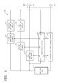
- FIG. 4 is a block diagram illustrating a battery pack 300 according to another embodiment.
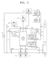
- FIG. 5 is a circuit diagram of the battery pack 300 of FIG. 4 .
- the battery pack 300 has structures and functions similar to those of the battery pack 100 illustrated in FIGS. 1 and 2 , and thus some differences between the battery pack 300 and the battery pack 100 are described.
- the battery pack 300 may further include a second converter circuit 361 and a third switching element 351.
- the first converter circuit 160 increases and decreases the input voltage, but in the present embodiment, a first converter circuit 360 increases the input voltage, and a second converter circuit 361 decreases the input voltage.
- the third switching element 351 is connected in series with a current path between a battery cell 310 and the second converter circuit 361 to form a charging path.
- the third switching element 351 is controlled to be in one of on and off states by a control signal from a protection circuit 330. When the third switching element 351 is in an on-state, an output voltage of the second converter circuit 361 is applied to the battery cell 310 as a charging voltage.
- a first switching element 340 includes the FET1 and the D1
- a second switching element 350 includes the FET2 and the D2
- the third switching element 351 includes a FET5 and a D5.
- all three switches are not controlled using only one control signal, and different control signals generated in a logic circuit 331 are applied to the FET1, the FET2, and the FET5, respectively.
- Each of the first through third switching elements 340, 350 and 351 form a path for charging.
- source electrodes of the FET1, FET2 and FET5 are connected to a positive electrode of the battery cell 310. Accordingly, when the battery cell 310 is charged, a charging current may be prevented from being supplied to the battery cell 310 simultaneously via the first switching element 340, the second switching element 350, and the third switching element 351.
- FIG. 6 is a flowchart illustrating a method of charging a battery pack 300.
- the method of charging the battery pack 300 in the present embodiment is similar to the method for the battery pack 100 illustrated in FIG. 3 , and thus certain differences therebetween are described.
- the battery pack 300 includes a circuit for increasing the output voltage of the charger and a circuit for decreasing the output voltage thereof.
- a logic circuit 331 does not need to control the first converter circuit 360 to increase or decrease the output voltage of the charger. Therefore, if the charging voltage is greater than the output voltage of the charger, the first converter circuit 360 increases the output voltage of the charger (operation S306). To allow the increased voltage to be applied to the battery cell 310, the logic circuit 331 applies a low-level control signal to the second switching element 350 to switch on the FET2 (operation S307). Accordingly, a current path through a positive electrode terminal 321, the first converter circuit 360, the FET2, the battery cell 310, the D4, the FET3, and a negative electrode terminal 322 is formed.
- the second converter circuit 360 decreases the output voltage of the charger (operation S308).
- the logic circuit 331 applies a low-level control signal to the third switching element 351 to switch on the FET5 (operation S309). Accordingly, a current path through the positive electrode terminal 321, the second converter circuit 361, the FET5, the battery cell 310, the D4, the FET3, and the negative electrode terminal 322 is formed.
- a program for executing methods of charging a battery pack according to the one or more of the above embodiments of the present invention may be stored in recording media.
- the term "recording media" used herein includes computer or processor readable media, and the recording media may be semiconductor recording media, for example, flash memories.
- the recording media is readable by a computer, and may be executed in a processor.
Landscapes
- Engineering & Computer Science (AREA)
- Power Engineering (AREA)
- Manufacturing & Machinery (AREA)
- Chemical & Material Sciences (AREA)
- Chemical Kinetics & Catalysis (AREA)
- Electrochemistry (AREA)
- General Chemical & Material Sciences (AREA)
- Secondary Cells (AREA)
- Charge And Discharge Circuits For Batteries Or The Like (AREA)
- Battery Mounting, Suspending (AREA)
Applications Claiming Priority (1)
| Application Number | Priority Date | Filing Date | Title |
|---|---|---|---|
| KR1020090131800A KR101097262B1 (ko) | 2009-12-28 | 2009-12-28 | 배터리 팩, 이의 충전방법 |
Publications (1)
| Publication Number | Publication Date |
|---|---|
| EP2367259A2 true EP2367259A2 (de) | 2011-09-21 |
Family
ID=44174938
Family Applications (1)
| Application Number | Title | Priority Date | Filing Date |
|---|---|---|---|
| EP10197007A Withdrawn EP2367259A2 (de) | 2009-12-28 | 2010-12-24 | Batteriepack und Verfahren zur Ladung eines Batteriepacks |
Country Status (5)
| Country | Link |
|---|---|
| US (1) | US8633677B2 (de) |
| EP (1) | EP2367259A2 (de) |
| JP (1) | JP5495443B2 (de) |
| KR (1) | KR101097262B1 (de) |
| CN (1) | CN102110864B (de) |
Cited By (1)
| Publication number | Priority date | Publication date | Assignee | Title |
|---|---|---|---|---|
| US10118498B2 (en) | 2013-03-21 | 2018-11-06 | Byd Company Limited | Power supply system for electric vehicle and method for controlling the same |
Families Citing this family (42)
| Publication number | Priority date | Publication date | Assignee | Title |
|---|---|---|---|---|
| JP6028499B2 (ja) * | 2012-04-06 | 2016-11-16 | ソニー株式会社 | 電力供給装置 |
| CN202906496U (zh) * | 2012-06-19 | 2013-04-24 | 无锡中星微电子有限公司 | 移动电源 |
| CN102751765B (zh) * | 2012-07-17 | 2014-08-13 | 无锡中星微电子有限公司 | 移动电源 |
| CN102751764B (zh) * | 2012-07-17 | 2014-09-10 | 无锡中星微电子有限公司 | 移动电源 |
| JP5791007B2 (ja) | 2012-08-07 | 2015-10-07 | ▲華▼▲為▼▲終▼端有限公司 | 電力供給の装置および方法ならびにユーザ装置 |
| CN103869858B (zh) * | 2012-12-11 | 2017-03-15 | 厦门雅迅网络股份有限公司 | 一种对车载电子设备电源的自适应控制方法及其系统 |
| TWI472785B (zh) * | 2013-07-19 | 2015-02-11 | Chen Tech Electric Mfg Co Ltd | Intelligent Scheduling System for Battery Test Production and Its |
| KR102247393B1 (ko) * | 2014-03-12 | 2021-05-03 | 삼성에스디아이 주식회사 | 배터리 팩 및 이의 제어방법 |
| WO2016013451A1 (ja) * | 2014-07-22 | 2016-01-28 | ローム株式会社 | 充電回路およびそれを利用した電子機器、充電器 |
| CN104218648A (zh) * | 2014-09-24 | 2014-12-17 | 苏州贝昂科技有限公司 | 一种充放电保护电路和充放电系统 |
| KR102335018B1 (ko) * | 2015-03-05 | 2021-12-02 | 삼성에스디아이 주식회사 | 충전 전압 제어 장치 |
| JP6441189B2 (ja) * | 2015-09-10 | 2018-12-19 | 東芝三菱電機産業システム株式会社 | 無停電電源装置 |
| DE102015221101B4 (de) * | 2015-10-28 | 2022-12-08 | Dialog Semiconductor (Uk) Limited | Batterieladeregler, Ladegerät zum Laden einer Batterie, tragbare elektronische Vorrichtung mit Ladegerät und Verfahren für einen Betrieb eines Ladegeräts |
| KR102516355B1 (ko) * | 2015-12-21 | 2023-03-31 | 삼성전자주식회사 | 배터리 제어 방법, 배터리 제어 장치, 및 배터리 팩 |
| US9515496B1 (en) * | 2016-03-21 | 2016-12-06 | Hangzhou Chic Intelligent Technology Co., Ltd | Battery management system for human-machine interaction vehicles |
| US11088549B2 (en) * | 2016-03-22 | 2021-08-10 | Intersil Americas LLC | Multiple chargers configuration in one system |
| US10594152B1 (en) | 2016-03-25 | 2020-03-17 | Intersil Americas LLC | Method and system for a battery charger |
| CN106026225B (zh) * | 2016-05-20 | 2020-05-08 | 深圳维普创新科技有限公司 | 充电电池的快速充电电路及充电方法 |
| DE102016109862A1 (de) * | 2016-05-30 | 2017-11-30 | Hella Kgaa Hueck & Co. | Schaltvorrichtung zum Schalten einer elektrischen Verbindung, Energiespeichersystem für ein Fahrzeug sowie Verfahren zum Schalten einer elektrischen Verbindung |
| JP6828296B2 (ja) * | 2016-08-09 | 2021-02-10 | 株式会社Gsユアサ | 蓄電装置および蓄電装置の充電制御方法 |
| KR102222119B1 (ko) | 2016-08-11 | 2021-03-03 | 삼성에스디아이 주식회사 | 배터리 팩 |
| WO2018068243A1 (zh) | 2016-10-12 | 2018-04-19 | 广东欧珀移动通信有限公司 | 移动终端 |
| CN107947252B (zh) | 2016-10-12 | 2020-09-22 | Oppo广东移动通信有限公司 | 终端和设备 |
| US10305312B2 (en) * | 2016-11-08 | 2019-05-28 | Lenovo (Singapore) Pte. Ltd. | Supplemental power system for battery powered device |
| GB2543225C (en) * | 2017-01-25 | 2020-02-19 | O2Micro Inc | Controlling power delivery to a battery |
| JP7059290B2 (ja) * | 2017-04-07 | 2022-04-25 | オッポ広東移動通信有限公司 | 無線充電装置、無線充電方法及び被充電機器 |
| AU2018249241B2 (en) * | 2017-04-07 | 2020-07-16 | Guangdong Oppo Mobile Telecommunications Corp., Ltd. | Wireless charging apparatus, device to be charged and control method therefor |
| WO2018184230A1 (zh) * | 2017-04-07 | 2018-10-11 | Oppo广东移动通信有限公司 | 无线充电系统、装置、方法及待充电设备 |
| KR102318241B1 (ko) | 2017-04-13 | 2021-10-27 | 광동 오포 모바일 텔레커뮤니케이션즈 코포레이션 리미티드 | 충전 대기 설비 및 충전 방법 |
| US11218006B2 (en) | 2017-04-13 | 2022-01-04 | Enphase Energy, Inc. | Method and system for an AC battery |
| DE102018005747A1 (de) | 2017-08-22 | 2019-02-28 | Sew-Eurodrive Gmbh & Co. Kg | Energiespeicheranordnung und Fahrzeug mit Energiespeicheranordnung |
| CN107453455B (zh) * | 2017-09-29 | 2020-06-05 | 上海摩软通讯技术有限公司 | 移动终端的充电方法及系统 |
| CN111279574B (zh) * | 2018-04-25 | 2024-03-22 | Oppo广东移动通信有限公司 | 终端设备和充电控制方法 |
| CN115632454B (zh) * | 2018-07-27 | 2023-10-13 | 荣耀终端有限公司 | 一种终端设备的供电电路、终端设备及供电方法 |
| CN109130948B (zh) * | 2018-09-12 | 2024-03-01 | 深圳市思达仪表有限公司 | 一种bms双辅源供电系统 |
| US11251707B2 (en) | 2019-01-30 | 2022-02-15 | Renesas Electronics America Inc. | Power delivery architecture for multiport systems |
| CN111262301B (zh) * | 2020-03-12 | 2023-04-07 | 福建飞毛腿动力科技有限公司 | 一种锂电池充电管理模块 |
| US11588336B2 (en) * | 2020-06-16 | 2023-02-21 | Semiconductor Components Industries, Llc | Methods and apparatus for a battery system |
| CN115498710A (zh) * | 2021-06-17 | 2022-12-20 | 中兴通讯股份有限公司 | 充电电路、充电方法、电子设备及存储介质 |
| CN115811104A (zh) * | 2021-09-14 | 2023-03-17 | 艾普凌科株式会社 | 单元平衡电路与装置、充放电控制电路与装置及电池装置 |
| JP2023118534A (ja) * | 2022-02-15 | 2023-08-25 | 株式会社Limno | 情報端末装置および情報端末システム |
| CN114498866B (zh) * | 2022-04-19 | 2022-07-29 | 伏达半导体(合肥)有限公司 | 双电池充电装置、方法及其控制器 |
Family Cites Families (17)
| Publication number | Priority date | Publication date | Assignee | Title |
|---|---|---|---|---|
| JPH06105476A (ja) | 1992-09-17 | 1994-04-15 | Sony Corp | 電池充電装置 |
| KR0181164B1 (ko) | 1996-07-06 | 1999-05-15 | 삼성전자주식회사 | 다종 배터리 공용 충전장치 및 그 제어방법 |
| JPH11185824A (ja) | 1997-10-15 | 1999-07-09 | Sony Corp | 一次電池互換バッテリーパック |
| JP4499966B2 (ja) | 2001-09-14 | 2010-07-14 | 株式会社リコー | 二次電池の充電回路 |
| US7012405B2 (en) | 2001-09-14 | 2006-03-14 | Ricoh Company, Ltd. | Charging circuit for secondary battery |
| US20040164711A1 (en) | 2003-02-25 | 2004-08-26 | Isao Hayashi | Battery charger and method therefor |
| JP4047194B2 (ja) * | 2003-02-25 | 2008-02-13 | キヤノン株式会社 | バッテリ充電装置およびその制御方法 |
| JP4133735B2 (ja) * | 2003-10-27 | 2008-08-13 | ソニー株式会社 | 電池パック |
| US7456614B2 (en) | 2003-10-27 | 2008-11-25 | Sony Corporation | Battery pack |
| US7737658B2 (en) | 2003-10-27 | 2010-06-15 | Sony Corporation | Battery packs having a charging mode and a discharging mode |
| JP4114592B2 (ja) | 2003-10-28 | 2008-07-09 | ソニー株式会社 | 電池パック |
| US6867588B1 (en) * | 2003-12-23 | 2005-03-15 | Intel Corporation | Nuclear spin resonance clock arrangements |
| KR100530691B1 (ko) | 2005-04-04 | 2005-11-29 | 주식회사 벡터전자 | 충전전압 자동 선택 배터리충전기 |
| JP2007060772A (ja) | 2005-08-23 | 2007-03-08 | Fuji Electric Device Technology Co Ltd | 充電電圧の切替え設定方式 |
| KR20080028170A (ko) | 2006-09-26 | 2008-03-31 | 엘지전자 주식회사 | 배터리 충전장치 및 방법 |
| US7863865B2 (en) * | 2007-07-26 | 2011-01-04 | Summit Microelectronics, Inc. | Systems and methods for pulse charging a battery |
| TW200919917A (en) * | 2007-10-19 | 2009-05-01 | Syspotek Corp | Power supply device with voltage conversion circuit |
-
2009
- 2009-12-28 KR KR1020090131800A patent/KR101097262B1/ko not_active Expired - Fee Related
-
2010
- 2010-09-01 JP JP2010195567A patent/JP5495443B2/ja not_active Expired - Fee Related
- 2010-12-24 EP EP10197007A patent/EP2367259A2/de not_active Withdrawn
- 2010-12-27 US US12/979,190 patent/US8633677B2/en not_active Expired - Fee Related
- 2010-12-28 CN CN201010623422.6A patent/CN102110864B/zh not_active Expired - Fee Related
Non-Patent Citations (1)
| Title |
|---|
| None |
Cited By (1)
| Publication number | Priority date | Publication date | Assignee | Title |
|---|---|---|---|---|
| US10118498B2 (en) | 2013-03-21 | 2018-11-06 | Byd Company Limited | Power supply system for electric vehicle and method for controlling the same |
Also Published As
| Publication number | Publication date |
|---|---|
| JP5495443B2 (ja) | 2014-05-21 |
| CN102110864A (zh) | 2011-06-29 |
| KR101097262B1 (ko) | 2011-12-21 |
| US8633677B2 (en) | 2014-01-21 |
| JP2011139622A (ja) | 2011-07-14 |
| CN102110864B (zh) | 2015-04-15 |
| KR20110075364A (ko) | 2011-07-06 |
| US20110156655A1 (en) | 2011-06-30 |
Similar Documents
| Publication | Publication Date | Title |
|---|---|---|
| EP2367259A2 (de) | Batteriepack und Verfahren zur Ladung eines Batteriepacks | |
| KR101182890B1 (ko) | 배터리 팩 충전 제어 시스템 | |
| KR101030885B1 (ko) | 이차전지 | |
| US8203309B2 (en) | Battery pack, and battery system | |
| US9077196B2 (en) | Battery pack and power generation circuit in battery pack | |
| KR101182430B1 (ko) | 배터리 팩 | |
| CN103001275B (zh) | 电池包、电子装置及电池包布置 | |
| TWI223917B (en) | Charging control circuit, charger, power supply circuit information processing device, and battery pack | |
| KR101201139B1 (ko) | 배터리 팩의 보호 회로 장치 | |
| US10090690B2 (en) | Secondary battery protection circuit | |
| KR101193170B1 (ko) | 배터리 팩 및 이의 제어방법 | |
| CN101350532A (zh) | 带有旁路的过电压保护电池充电器 | |
| US20110248676A1 (en) | Battery pack | |
| JP2005168159A (ja) | 過電流保護回路と充電式電池パック | |
| JPH08190936A (ja) | 二次電池の充放電保護装置 | |
| US8786258B2 (en) | Battery pack and method of controlling the battery pack | |
| JP2005168160A (ja) | 過電流保護回路と充電式電池パック | |
| JP2002093466A (ja) | 充電制御回路 | |
| KR20060011484A (ko) | 배터리 팩 | |
| KR20260051956A (ko) | 이차전지 보호 집적 회로, 전원 시스템 및 배터리 장치 |
Legal Events
| Date | Code | Title | Description |
|---|---|---|---|
| PUAI | Public reference made under article 153(3) epc to a published international application that has entered the european phase |
Free format text: ORIGINAL CODE: 0009012 |
|
| 17P | Request for examination filed |
Effective date: 20101224 |
|
| AK | Designated contracting states |
Kind code of ref document: A2 Designated state(s): AL AT BE BG CH CY CZ DE DK EE ES FI FR GB GR HR HU IE IS IT LI LT LU LV MC MK MT NL NO PL PT RO RS SE SI SK SM TR |
|
| AX | Request for extension of the european patent |
Extension state: BA ME |
|
| STAA | Information on the status of an ep patent application or granted ep patent |
Free format text: STATUS: REQUEST FOR EXAMINATION WAS MADE |
|
| STAA | Information on the status of an ep patent application or granted ep patent |
Free format text: STATUS: THE APPLICATION IS DEEMED TO BE WITHDRAWN |
|
| 18D | Application deemed to be withdrawn |
Effective date: 20170701 |