EP2363789B1 - Appareil de détection de position - Google Patents
Appareil de détection de position Download PDFInfo
- Publication number
- EP2363789B1 EP2363789B1 EP11151058.2A EP11151058A EP2363789B1 EP 2363789 B1 EP2363789 B1 EP 2363789B1 EP 11151058 A EP11151058 A EP 11151058A EP 2363789 B1 EP2363789 B1 EP 2363789B1
- Authority
- EP
- European Patent Office
- Prior art keywords
- sensor
- conductors
- circuit
- position detection
- signal
- Prior art date
- Legal status (The legal status is an assumption and is not a legal conclusion. Google has not performed a legal analysis and makes no representation as to the accuracy of the status listed.)
- Not-in-force
Links
- 238000001514 detection method Methods 0.000 title claims description 104
- 239000004020 conductor Substances 0.000 claims description 142
- 230000005540 biological transmission Effects 0.000 claims description 85
- 230000010355 oscillation Effects 0.000 claims description 21
- 238000000034 method Methods 0.000 claims description 12
- 230000005674 electromagnetic induction Effects 0.000 description 29
- 239000003990 capacitor Substances 0.000 description 11
- 238000010586 diagram Methods 0.000 description 8
- 230000004044 response Effects 0.000 description 8
- 230000001360 synchronised effect Effects 0.000 description 8
- 230000006698 induction Effects 0.000 description 6
- 238000004804 winding Methods 0.000 description 6
- 230000001681 protective effect Effects 0.000 description 5
- 238000001228 spectrum Methods 0.000 description 5
- 239000000758 substrate Substances 0.000 description 5
- 239000002131 composite material Substances 0.000 description 3
- 230000006866 deterioration Effects 0.000 description 3
- 230000007274 generation of a signal involved in cell-cell signaling Effects 0.000 description 3
- 239000004925 Acrylic resin Substances 0.000 description 2
- 229920000178 Acrylic resin Polymers 0.000 description 2
- 239000011521 glass Substances 0.000 description 2
- 230000008054 signal transmission Effects 0.000 description 2
- 230000007704 transition Effects 0.000 description 2
- 230000008602 contraction Effects 0.000 description 1
- 230000008878 coupling Effects 0.000 description 1
- 238000010168 coupling process Methods 0.000 description 1
- 238000005859 coupling reaction Methods 0.000 description 1
- 230000009977 dual effect Effects 0.000 description 1
- 238000000605 extraction Methods 0.000 description 1
- AMGQUBHHOARCQH-UHFFFAOYSA-N indium;oxotin Chemical compound [In].[Sn]=O AMGQUBHHOARCQH-UHFFFAOYSA-N 0.000 description 1
- 239000004973 liquid crystal related substance Substances 0.000 description 1
- 230000008569 process Effects 0.000 description 1
- 239000012780 transparent material Substances 0.000 description 1
Images


Classifications
-
- G—PHYSICS
- G06—COMPUTING; CALCULATING OR COUNTING
- G06F—ELECTRIC DIGITAL DATA PROCESSING
- G06F3/00—Input arrangements for transferring data to be processed into a form capable of being handled by the computer; Output arrangements for transferring data from processing unit to output unit, e.g. interface arrangements
- G06F3/01—Input arrangements or combined input and output arrangements for interaction between user and computer
- G06F3/03—Arrangements for converting the position or the displacement of a member into a coded form
- G06F3/041—Digitisers, e.g. for touch screens or touch pads, characterised by the transducing means
- G06F3/046—Digitisers, e.g. for touch screens or touch pads, characterised by the transducing means by electromagnetic means
-
- G—PHYSICS
- G06—COMPUTING; CALCULATING OR COUNTING
- G06F—ELECTRIC DIGITAL DATA PROCESSING
- G06F3/00—Input arrangements for transferring data to be processed into a form capable of being handled by the computer; Output arrangements for transferring data from processing unit to output unit, e.g. interface arrangements
- G06F3/01—Input arrangements or combined input and output arrangements for interaction between user and computer
- G06F3/03—Arrangements for converting the position or the displacement of a member into a coded form
- G06F3/041—Digitisers, e.g. for touch screens or touch pads, characterised by the transducing means
- G06F3/044—Digitisers, e.g. for touch screens or touch pads, characterised by the transducing means by capacitive means
- G06F3/0446—Digitisers, e.g. for touch screens or touch pads, characterised by the transducing means by capacitive means using a grid-like structure of electrodes in at least two directions, e.g. using row and column electrodes
-
- G—PHYSICS
- G06—COMPUTING; CALCULATING OR COUNTING
- G06F—ELECTRIC DIGITAL DATA PROCESSING
- G06F2203/00—Indexing scheme relating to G06F3/00 - G06F3/048
- G06F2203/041—Indexing scheme relating to G06F3/041 - G06F3/045
- G06F2203/04106—Multi-sensing digitiser, i.e. digitiser using at least two different sensing technologies simultaneously or alternatively, e.g. for detecting pen and finger, for saving power or for improving position detection
Definitions
- This invention relates to a technique suitable for application to a position detection apparatus wherein a plurality of position detection systems are combined. More particularly, the present invention relates to a position detection apparatus wherein a position detection system of an electromagnetic type for detecting a position pointed to, for example, by a position pointing device (pen) as a pointer is combined with a position detection system of a capacitive type for detecting a position pointed to, for example, by a finger as a pointer.
- a touch panel apparatus is available wherein a position detection apparatus for detecting a pointed position by a pointer is combined with a display area of a liquid crystal display apparatus.
- the touch panel apparatus is an inputting apparatus whose display face is touched by a finger or a pen as a pointer to carry out operation of a computer or the like, and detects a position on the screen touched by a finger or a pen to provide an instruction to a computer.
- This touch panel is utilized widely in a PDA (Personal Digital Assistant), an ATM (Automated Teller Machine), a ticket-vending machine in a railway station and so forth.
- a resistive type system wherein position detection is carried out based on a variation of the resistance, which is caused by the pressure applied to the touch panel by a pointer
- a capacitive system wherein position detection is carried out based on a variation of the capacitance between sensor conductors, and so forth are available.
- a cursor input device with dual input modes including a control computing module, a coordinate sensing module, a first analog multiplexing module, a first signal processing module, a second analog multiplexing module and a second signal processing module, where the coordinate sensing module further including a touch sensing loop unit and an electromagnetic sensing loop unit.
- the control computing module uses the first analog multiplexing unit and the first signal processing module to enable the electromagnetic sensing loop unit to perform signal scanning and processing, and uses the second analog multiplexing unit and the second signal processing module to enable the touch sensing loop unit to perform signal scanning and processing.
- WO 2008/007118 A2 discloses a transducer for a position sensor comprising a single laminate sensor board carrying a plurality of windings formed by conductors on layers of the sensor board, the windings being arrayed over a first area of the sensor board; and detection circuitry mounted on another layer of the sensor board over a second area of the circuit board and electrically coupled to said windings.
- the detection circuitry has a first mode of operation in which signals inductively coupled to or from said windings are detected and a second mode of operation in which signals capacitively coupled to or from said windings are detected.
- the windings and detection circuitry are arranged on the sensor board so that said first and second areas oppose each other.
- a position detection apparatus which uses a combination of a plurality of position detection systems in order to detect a pen and a finger as pointers at the same time.
- the pointer position detection section of the electromagnetic system generates an alternating magnetic field having a predetermined frequency in order to cause a resonance circuit, which is incorporated in a pen as a position pointer, to resonate.
- This alternating magnetic field sometimes has an influence as noise on the position detection section of the capacitive type system and sometimes gives rise to deterioration of the position detection performance by the capacitive type system.
- the present invention has been made in view of such a point as described above, and according to one aspect of the present invention a position detection apparatus incorporating a plurality of position detection systems is provided, wherein interference of transmission signals when these position detection systems operate at the same time can be suppressed thereby to prevent deterioration of a detection performance of the position pointed to by a pointer such as a pen or a finger to achieve a stabilized position pointing performance.
- selection position information of a transmission conductor in a first position detection system is utilized for selecting a reception conductor in a second position detection system thereby to increase the spatial distance between the transmission conductor in the first position detection system and the reception conductor in the second position detection system as much as possible.
- a relationship of frequency interleave is provided between a transmission signal to be supplied to the transmission conductor in the first position detection system and another transmission signal to be supplied to the transmission conductor in the second position detection system.
- the position detection apparatus in the position detection apparatus wherein a plurality of position detection systems are combined and operated simultaneously with each other, such a situation that a transmission signal to a sensor conductor used by one of the position detection apparatus is received as noise by the other position detection apparatus to have a negative influence can be suppressed effectively. Consequently, the position detection apparatus can be provided which prevents deterioration of the position detection performance and can achieve a stabilized position detection function.
- the invention concerns a position detecting apparatus and method according to the appended claims.
- FIGS. 1 to 8 embodiments of the present invention are described with reference to FIGS. 1 to 8 .
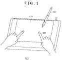
- FIG. 1 is a perspective view of an entire position detection apparatus showing an example of a first embodiment of the present invention.
- the position detection apparatus 101 includes a position detection region 104 for detecting the positions pointed to by a pen 102 as a first position pointer and a finger 105 as a second position pointer, and position information corresponding to an operation of the pen 102 and the finger 105 is supplied to an apparatus such as a personal computer (not shown). Further, a transparent protective cover of a glass plate, an acrylic resin plate or the like, hereinafter described, is disposed on the position detection region 104, and a display section such as a known LCD display unit is disposed below the protective cover. The LCD display unit displays a signal supplied thereto from the apparatus such as a personal computer.
- a user can draw on the LCD display unit.
- a user can expand (enlarge), contract (shrink), or rotate an image displayed on the LCD display unit.
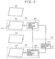
- FIG. 2 is a block diagram illustrating a general internal configuration of the position detection apparatus 101.
- a protective cover 202 is formed of a transparent material, such as a glass plate or an acrylic resin plate, in order to physically protect the position detection region 104 and to allow a display image on an LCD display unit 203 disposed underneath to be transmitted therethrough.
- a capacitive sensor 204 is disposed below the protective cover 202. In the capacitive sensor 204, a plurality of transparent electrodes of an ITO (Indium Tin Oxide) film or the like are disposed in a first direction and a second direction intersecting with the first direction to form a sensor of a grid structure, and the position pointed to by the finger 105 on the position detection region 104 is detected.
- ITO Indium Tin Oxide
- the capacitive sensor 204 is connected to a capacitive signal processing section 205 and detects a capacitance variation of a capacitor formed at a crossing point of a plurality of transparent electrodes which form the capacitive sensor 204 to detect the pointing position of the finger 105. It is to be noted that the capacitive sensor 204 and the capacitive signal processing section 205 form a capacitive type position detection section 206.
- the LCD display unit 203 is disposed below the capacitive sensor 204 and displays a video signal 212 supplied thereto from the apparatus such as the personal computer.
- An electromagnetic induction coil sensor 207 is disposed below the LCD display unit 203.
- the electromagnetic induction coil sensor 207 is formed of a plurality of loop coils. The individual loop coils are disposed in the first direction and the second direction different from the first direction similarly as in the electrode disposition structure of the capacitive sensor 204 to form a sensor of a grid structure.
- the electromagnetic induction coil sensor 207 is connected to an electromagnetic signal processing section 208.
- the electromagnetic induction coil sensor 207 and the electromagnetic signal processing section 208 form an electromagnetic type position detection section 209.
- the electromagnetic signal processing section 208 successively supplies a transmission signal, that is, an AC signal having a predetermined frequency, for a predetermined period of time to each of the loop coils which form the electromagnetic induction coil sensor 207, and then switches over the loop coils so that they function as reception coils to detect an induction magnetic field generated by the pen 102.
- a transmission signal that is, an AC signal having a predetermined frequency
- the coil which forms the resonance circuit Based on this electric current, the coil which forms the resonance circuit generates the induction magnetic field. Even if the AC signal supplied to the loop coil is stopped, the induction magnetic field continues to be generated for a predetermined period of time. By detecting the induction magnetic field by means of the loop coil which is in a signal receiving state, the position of the pen 102 as a position pointer is detected.
- the electromagnetic type position detection section 209 detects the position of the pen 102 based on mutual electromagnetic induction with the pen 102, even if the pen 102 and the electromagnetic induction coil sensor 207 are spaced from each other by some distance, the electromagnetic type position detection section 209 can detect the position pointed to by the pen 102.
- the capacitive type position detection section 206 of the capacitive type detects a capacitance variation of a capacitor caused by close approaching of the finger 105 as a position pointer to the electrodes, preferably the distance from the capacitive sensor 204 to the finger 105 is as small as possible. Therefore, in the illustrated embodiment, the capacitive sensor 204 is disposed immediately below the protective cover 202, and the electromagnetic induction coil sensor 207 is disposed below the capacitive sensor 204 with the LCD display unit 203 interposed therebetween.
- Pointed position data outputted from the capacitive signal processing section 205 and pointed position data outputted from the electromagnetic signal processing section 208 are inputted to an output signal generation section 210.
- the output signal generation section 210 converts the two pointed position data into data of a predetermined transmission format and outputs the pointed position data of the predetermined transmission format as an output signal 211 to an externally connected apparatus such as a personal computer (not shown). It is to be noted that the personal computer side separates the two received pointed position data and, for example, incorporates and utilizes the pointed position data in application software.
- the LCD display unit 203 interposed between the capacitive sensor 204 and the electromagnetic induction coil sensor 207 receives a video signal 212 supplied thereto from the externally connected apparatus such as the personal computer and carries out predetermined display.
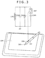
- FIG. 3 shows a configuration of a resonance circuit provided in the pen 102.
- a coil L302, a capacitor C303 and a semi-fixed capacitor C304 are connected in parallel and form a known resonance circuit.
- the resonance circuit resonates in response to reception of an alternating magnetic field from loop coils 408 (408a to 408d) which form the electromagnetic induction coil sensor 207 shown in FIG. 4 , and generates an alternating magnetic field based on a resonance frequency of the resonance circuit after transmission of the alternating magnetic field from the loop coils 408 stops, and supplies the alternating magnetic field to the loop coils 408 which form the electromagnetic induction coil sensor 207.
- the loop coils 408 are switched over so as to function as reception coils for receiving a signal from the pen 102.
- a capacitor C305 and a pushbutton switch 307 which operates in an interlocked relationship with an operation of a pushbutton 306 provided on a side face of the pen 102, are connected in series to each other and are connected in parallel to the coil L302, capacitor C303 and semi-fixed capacitor C304. Accordingly, if the pushbutton switch 307 is controlled between on and off, then the composite capacitance of the capacitors which form the resonance circuit varies, and as a result, the resonance frequency of the resonance circuit varies in response to the state of the pushbutton switch 307. By discriminating the variation of the resonance frequency, the position detection apparatus 101 can determine not only the position pointed to by a pen tip 309 but also the operation state of the pushbutton 306.
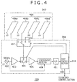
- FIG. 4 is a block diagram of the electromagnetic type position detection section 209.
- An oscillation circuit 402 generates a sine wave AC signal or a square wave signal of a frequency substantially equal to the resonance frequency of the resonance circuit of the pen 102 described hereinabove, and supplies the generated signal to a current driver 403 and a synchronous detector 404.
- the current driver 403 current-amplifies the signal of the predetermined frequency oscillated by the oscillation circuit 402 and supplies the amplified signal to a transmission/reception switching circuit 405.
- the transmission/reception switching circuit 405 selectively connects one of an output terminal of the current driver 403 and an input terminal of a reception amplifier 406 to a coil selection circuit 407.
- the coil selection circuit 407 selects one of a plurality of loop coils 408a, 408b, 408c and 408d which form the electromagnetic induction coil sensor 207 and connects the selected loop coil to the transmission/reception switching circuit 405.
- the coil selection circuit 407 and the current driver 403 are connected to each other through the transmission/reception switching circuit 405, a signal supplied from the current driver 403 is supplied to the loop coils 408a, 408b, 408c and 408d successively selected under the coil-selection control of the coil selection circuit 407.
- the coil selection circuit 407 and the reception amplifier 406 are connected to each other through the transmission/reception switching circuit 405, signals received by the loop coils 408a, 408b, 408c and 408d under the coil-selection control of the coil selection circuit 407 are inputted to the reception amplifier 406. It is to be noted that selection for the transmission/reception switching circuit 405 and the coil selection circuit 407 are controlled by control signals supplied thereto from a first control section 409 hereinafter described.
- the loop coils 408a, 408b, 408c and 408d of a substantially rectangular shape are juxtaposed in parallel to each other on the same plane.
- the loop coils 408a, 408b, 408c and 408d are connected at one terminal thereof to the coil selection circuit 407 and grounded at the other terminal thereof.
- one of the loop coils selected by the coil selection circuit 407 is connected to the output terminal of the current driver 403 through the transmission/reception switching circuit 405
- an alternating magnetic field is generated from one of the loop coils selected by the coil selection circuit 407 in response to a signal supplied thereto from the current driver 403. Accordingly, when the pen 102 is positioned in the neighborhood of a loop coil from which an alternating magnetic is generated, induction electromotive force is generated in the resonance circuit in the pen 102.
- the loop coil is placed into a state in which it can receive an alternating magnetic field generated by the resonance circuit of the pen 102. If the loop coil 408 receives an alternating magnetic field generated by the resonance circuit of the pen 102, then a weak AC signal is generated in the loop coil 408.
- the reception amplifier 406 converts the current into a voltage and amplifies the voltage and supplies the amplified voltage to the input terminal of the synchronous detector 404.
- the electromagnetic type position detection section 209 is in a signal transmitting state to the pen 102.
- the electromagnetic type position detection section 209 is in a signal receiving state from the pen 102.
- loop coils 408a, 408b, 408c and 408d which form the electromagnetic induction coil sensor 207, in parallel to each other in the first direction, and disposing another electromagnetic induction coil sensor 207 having a similar configuration but with its loop coils arranged in the second direction different from the first direction, a two-dimensional position, that is, an X coordinate and a Y coordinate of a position pointed to on the position detection region 104 by the pen 102 can be detected.
- An A/D converter 411 converts an analog signal from the synchronous detector 404 into a digital signal.
- the synchronous detector 404 is known and includes an analog multiplier such that a signal obtained by multiplication of a signal from the oscillation circuit 402 and a reception signal is outputted. Where the signal from the oscillation circuit 402 and the reception signal have frequencies coincident with each other, the synchronous detector 404 outputs a high signal level, but where the signal from the oscillation circuit 402 and the reception signal have frequencies different from each other, the output signal level of the synchronous detector 404 drops. It is to be noted that a variation of the frequency is caused by a variation of the resonance frequency of the resonance circuit of the pen 102.
- the composite capacitance of the capacitors which form the resonance circuit varies, and the level of the signal obtained from the synchronous detector 404 varies in response to the variation of the composite capacitance.
- the frequency variation of the AC magnetic field generated by the pen 102 can be detected, and from this frequency variation, the operation state of the pushbutton 306 provided in the pen 102 can be detected.
- FIG. 5 is a block diagram of the capacitive type position detection section 206. Functions and operation of the capacitive type position detection section 206 are described with reference to FIG. 5 .
- a second control section 503 supplies a transmission conductor selection signal for selecting transmission conductors 504 in a predetermined sequence to a transmission conductor selection circuit 502. Accordingly, an AC signal generated by an oscillation circuit 501 and having a predetermined frequency is successively supplied to the transmission conductors 504, which form the capacitive sensor 204, through the transmission conductor selection circuit 502. Also a reception conductor selection circuit 505 is controlled based on a reception conductor selection signal from the second control section 503.
- reception conductors 506 which form the capacitive sensor 204 are successively selected and connected to an A/D converter 508 in accordance with a predetermined reception conductor selection sequence.
- the A/D converter 508 converts a signal from a reception conductor 506 selected by the reception conductor selection circuit 505 into digital data.
- the second control section 503 controls the transmission conductor selection circuit 502 to determine a transmission conductor 504 to which an AC signal is to be supplied, and receives a signal from a reception conductor 506 through the reception conductor selection circuit 505 and the A/D converter 508, and determines and supplies presence or absence or pointed position information of the finger 105 on the position detection region 104 to the output signal generation section 210.
- a transmission signal to a sensor conductor which is used by one of the position detection apparatus sometimes has a negative influence as noise on the other position detection apparatus.
- a signal from the oscillation circuit 402 provided in the electromagnetic type position detection section 209 of an electromagnetic induction system emitted through the respective loop coils 408 which form the electromagnetic induction coil sensor 207 may have a negative influence when received by a reception conductor 506 which forms the capacitive sensor 204 provided in the capacitive type position detection section 206 of a capacitive type system.
- a transmission signal generated by the oscillation circuit 501 provided in the capacitive type position detection section 206 of a capacitive type system and emitted from the transmission conductor 504 which forms the capacitive sensor 204 may be received as noise similarly when the loop coils 408 which form the electromagnetic induction coil sensor 207 provided in the electromagnetic type position detection section 209 of an electromagnetic induction system are in a state in which they function as reception coils.
- FIG. 6 illustrates a spatial disposition relationship between the electromagnetic induction coil sensor 207 and the capacitive sensor 204.
- the electromagnetic induction coil sensor 207 on which the loop coils 408 extend in the Y-axis direction and are disposed in parallel to each other in the X-axis direction
- the capacitive sensor 204 on which the reception conductors 506 that extend in the Y-axis direction and are disposed in parallel to each other in the X-axis direction are disposed in a superposed relationship with each other, with the LCD display unit 203 interposed therebetween though not shown.
- the loop coils 408 are in a state in which they are transmitting an alternating magnetic field to the pen 102. Further, while in FIG.
- the loop coils 408 are disposed on one of the faces of a substrate which forms the electromagnetic induction coil sensor 207, loop coils 408 having an orthogonal disposition relationship to the loop coils 408 shown are also formed on the other face of the substrate such that, by this configuration, the position pointed to by the pen 102 can be detected two-dimensionally (X/Y coordinates).
- the transmission conductors 504 having an orthogonal relationship to the reception conductors 506 are also formed on the other face of the substrate, such that the position pointed to by the finger 105 as a pointer can be detected two-dimensionally (X/Y coordinates) in cooperation with the reception conductors 506.
- the loop coils 408, which form the electromagnetic induction coil sensor 207 and perform the function of alternating magnetic field transmission, and the reception conductors 506 that form the capacitive sensor 204 are disposed such that their extending directions and parallel disposition directions are spatially the same. It is to be noted that, in the embodiment shown in FIG. 6 , the extending direction is in the Y direction and the parallel disposition direction is in the X direction.
- the first embodiment of the present invention when an alternating magnetic field is transmitted from a particular loop coil 408 to the pen 102 through the coil selection circuit 407 which forms the electromagnetic type position detection section 209 shown in FIG. 4 , information of such a selected coil position is supplied from the first control section 409 to the second control section 503 which forms the capacitive type position detection section 206 shown in FIG. 5 .
- the second control section 503 acquires the selection information of a loop coil for transmission of an alternating magnetic field and controls the selection position of a reception conductor 506 for determining the pointing position of the finger 105 as a pointer in accordance with the selection information.
- the second control section 503 controls the reception conductor selection circuit 505 based on the selection information of the loop coil for transmission supplied from the first control section 409 so that a reception conductor 506 disposed substantially at the center on the capacitive sensor 204 is selected.
- the reception conductors 506 are successively selected in the same direction along the X-axis direction, similarly. Consequently, a predetermined distance is always assured between the selected loop coil 408 and the selected reception conductor 506.
- the selective control of the reception conductors is carried out based on the selection position information of a transmission conductor
- reception conductors based on the selection position information of the transmission conductors 504; (2) the selective control of the reception conductors 506 based on the selection position information of the loop coils 408 as the transmission conductors; (3) the selective control of the loop coils 408 as the transmission conductors based on the selection position information of the reception conductors 506; and (4) the selective control of the transmission conductors 504 based on the selection position information of the loop coils 408 (not shown), having an orthogonal disposition relationship to the loop coils 408 shown in FIG. 4 , as the reception conductors.
- the present invention is not limited to the present embodiment. It is only necessary for the selection position of a loop coil 408 for transmitting an alternating magnetic field and the selection position of a reception conductor 506 to be individually controlled so that a certain predetermined distance may be assured between the two selection positions.
- the selection position of a reception conductor 506 is controlled in an associated relationship with the selection position of a loop coil 408.
- each of the electromagnetic induction coil sensor 207 and the capacitive sensor 204 loop coils and conductors which have an orthogonally disposed relationship are disposed on one face and the other face of a substrate.
- the reception conductors 506 which form the capacitive sensor 204 and have a disposition direction similar to the disposition direction of the loop coils 408 for transmission of an alternating magnetic field which form the electromagnetic induction coil sensor 207 are used for addressing a technical problem to be solved.
- the loop coils 408 disposed on one face of the electromagnetic induction coil sensor 207 and the loop coils 408 disposed on the other face of the electromagnetic induction coil sensor 207 are selectively used to function as the loop coils for transmission of an alternating magnetic field, in response to a selection operation of the loop coils 408 extending in the Y direction as shown in FIG. 4 as the transmission conductors, the reception conductors 506 which also extend in the Y direction and are forming the capacitive sensor 204 as shown in FIG. 5 , i.e., the reception conductors 506 having a similar disposition relationship to the loop coils 408 selected as the transmission conductors, are selected.
- FIG. 7A illustrates a signal supplied to the loop coils 408 provided in the electromagnetic type position detection section 209 (referred to as “EMR (Electro-Magnetic Resonance) driving signal") and FIG. 7B illustrates a signal supplied to the transmission conductors 504 provided in the capacitive type position detection section 206 (referred to as capacitive driving signal).
- EMR Electro-Magnetic Resonance
- the oscillation circuit 402 shown in FIG. 4 generates a sine wave AC signal of a frequency (e.g., 500 KHz) substantially equal to the resonance frequency of the resonance circuit of the pen 102.
- the loop coils 408 include four loop coils 408a, 408b, 408c and 408d for the convenience of description, and each of the coils is placed into a selected state for a period of 64 ⁇ S by the coil selection circuit 407, which is controlled by a predetermined sequence in accordance with an instruction from the first control section 409. Further, the selection operation of the coils is repeated for one cycle of 256 ⁇ S.
- switching control of the coils is carried out at intervals of a signal transmission period of 28 ⁇ S, a switching transition period of 4 ⁇ S, and a signal reception period of 32 ⁇ S, by the transmission/reception switching circuit 405 that carries out switching control in accordance with an instruction from the first control section 409. Accordingly, in the signal transmission period of 28 ⁇ S, the sine wave signal of 500 KHz generated by the oscillation circuit 402 is supplied to the coil.
- the sine wave signal of 250 KHz, for example, generated by the oscillation circuit 501 shown in FIG. 5 is supplied to the conductors which form the transmission conductors 504 through the transmission conductor selection circuit 502.
- the transmission conductor selection circuit 502 supplies the sine wave signal, which is generated by the oscillation circuit 501 in accordance with the predetermined transmission conductor selection sequence based on a control signal from the second control section 503, to a desired transmission conductor 504.
- each of the conductors which form the transmission conductors 504 is successively selected for every 128 ⁇ S (i.e., one conductor per 128 ⁇ S).
- the sine wave signal generated by the oscillation circuit 501 is supplied for a period of 128 ⁇ S to each of the conductors which form the transmission conductors 504 through the transmission conductor selection circuit 502. In other words, the sine wave signal generated by the oscillation circuit 501 is supplied intermittently to each of the transmission conductors 504.
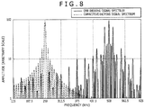
- FIG. 8 illustrates frequency spectra of the two types of transmission signals (EMR driving signal and capacitive driving signal) illustrated in FIGS. 7A and 7B , respectively.
- EMR driving signal and capacitive driving signal the two types of transmission signals illustrated in FIGS. 7A and 7B , respectively.
- the intermittent signal of 500 KHz illustrated in FIG. 7A side lobes are generated on peripheries around a main lobe of 500 KHz.
- the intermittent signal of 250 KHz illustrated in FIG. 7B side lobes are generated on peripheries around a main lobe of 250 KHz.
- the transmission signal illustrated in FIG. 7A and the transmission signal illustrated in FIG. 7B have a relationship of frequency interleave, that is, a relationship in which the frequency spectrum of the transmission signal illustrated in FIG.
- the oscillation circuit 402 shown in FIG. 4 and the oscillation circuit 501 shown in FIG. 5 are controlled by the first control section 409 and the second control section 503, respectively, so as to control at least one of the frequency of the oscillation circuit 402 and the frequency of the oscillation circuit 501 in association with the frequency of the other circuit in order to maintain the relationship of frequency interleave.
- the relationship of frequency interleave exists between the transmission signal illustrated in FIG. 7A and the transmission signal illustrated in FIG. 7B
- signal interference from the other detection section can be eliminated appropriately by using a noise removing filter.
- the signal to be supplied to the transmission conductors is not limited to a sine wave signal, but naturally it is possible to apply a rectangular wave signal, a pulse signal and so forth as well.
- the resonance frequency of the resonance circuit varies in response to the state of the pushbutton switch 307 as described hereinabove with reference to FIG. 3 .
- the deviation of the resonance frequency of the resonance circuit is defined so as to correspond to the spectrum of the EMR driving signal illustrated in FIG. 8 .
- the EMR driving signal has a transmission period of 28 ⁇ S and a switching transition period of 4 ⁇ S as illustrated in FIG. 7A , it has frequency components disposed at frequency intervals of 1/(28 ⁇ S + 4 ⁇ S), that is, 31.25 KHz. Accordingly, by setting the capacitance value of the capacitor C305 shown in FIG.
Landscapes
- Engineering & Computer Science (AREA)
- General Engineering & Computer Science (AREA)
- Theoretical Computer Science (AREA)
- Physics & Mathematics (AREA)
- Human Computer Interaction (AREA)
- General Physics & Mathematics (AREA)
- Electromagnetism (AREA)
- Position Input By Displaying (AREA)
- Measurement Of Length, Angles, Or The Like Using Electric Or Magnetic Means (AREA)
- Transmission And Conversion Of Sensor Element Output (AREA)
- Near-Field Transmission Systems (AREA)
Claims (15)
- Appareil de détection de position (101), comprenant :un premier circuit de détection de position (209) incluant un premier capteur (207) formé d'un premier ensemble de conducteurs (408) disposé dans une première direction et d'un deuxième ensemble de conducteurs disposé dans une direction différente de la première direction, un premier circuit de sélection de conducteurs (407) connecté audit premier capteur et configuré de manière à sélectionner le premier ensemble de conducteurs (408) selon une séquence de sélection de conducteurs de transmission, et un circuit d'oscillation (402) configuré de manière à fournir un signal au premier ensemble de conducteurs (408) à travers ledit premier circuit de sélection de conducteurs (407), le premier circuit de détection de position (209) étant configuré de manière à détecter une position pointée par un premier pointeur (102) sur ledit premier capteur (207) ;un second circuit de détection de position (206) incluant un second capteur (204) formé d'un troisième ensemble de conducteurs (506) disposé sensiblement dans la même direction que la première direction et d'un quatrième ensemble de conducteurs (504) disposé dans une direction différente de la première direction, le second capteur (204) étant disposé dans une relation de superposition avec ledit premier capteur (207), et un deuxième circuit de sélection de conducteurs (505) connecté audit second capteur (204) et configuré de manière à sélectionner le troisième ensemble de conducteurs (506) disposé sensiblement dans la même direction que la première direction selon une séquence de sélection de conducteurs de réception, le second circuit de détection de position (206) étant configuré de manière à détecter une position pointée par un second pointeur (105) sur ledit second capteur (206) ; etcaractérisé parun circuit de commande (409) configuré de manière à commander audit premier circuit de sélection de conducteurs (407) de sélectionner une position de sélection de conducteurs de transmission parmi le premier ensemble de conducteurs (408), et à commander audit deuxième circuit de sélection de conducteurs (505) de sélectionner une position de sélection de conducteurs de réception parmi le troisième ensemble de conducteurs (506), de sorte que la position de sélection de conducteurs de transmission sélectionnée et que la position de sélection de conducteurs de réception sélectionnée sont séparées l'une de l'autre d'une distance prédéterminée dans la première direction.
- Appareil de détection de position selon la revendication 1, dans lequel les conducteurs du premier ensemble de conducteurs (408) disposé dans la première direction sont formés chacun d'un enroulement en boucle, et le premier circuit de détection de position (209) comprend en outre un circuit de commutation de transmission / réception (405) configuré de manière à commuter par répartition dans le temps entre la fourniture d'un signal du circuit d'oscillation (402) à l'enroulement en boucle sélectionné par ledit premier circuit de sélection de conducteurs (407), et la réception d'un signal à partir de l'enroulement en boucle sélectionné par ledit premier circuit de sélection de conducteurs.
- Appareil de détection de position selon la revendication 1 ou 2, dans lequel ledit premier circuit de détection de position (209) est configuré de manière à détecter électromagnétiquement une position pointée par le premier pointeur (102), en transmettant un signal à partir de l'un quelconque des enroulements en boucle à travers ledit circuit de commutation de transmission / réception (405) afin qu'il soit reçu par un circuit de résonance dans le premier pointeur (102), et en recevant un signal émis à partir du circuit de résonance avec les enroulements en boucle.
- Appareil de détection de position selon l'une quelconque des revendications précédentes, dans lequel le circuit de commande (409) est configuré de manière à commander audit deuxième circuit de sélection de conducteurs (505) de sélectionner une position de sélection de conducteurs de réception séparée par la distance prédéterminée de la position de sélection de conducteurs de transmission qui a été sélectionnée par ledit premier circuit de sélection de conducteurs (407).
- Appareil de détection de position selon l'une quelconque des revendications précédentes, dans lequel le circuit de commande (409) est configuré de manière à commander audit premier circuit de sélection de conducteurs (505) de sélectionner une position de sélection de conducteurs de transmission séparée par la distance prédéterminée de la position de sélection de conducteurs de réception qui a été sélectionnée par ledit deuxième circuit de sélection de conducteurs (407).
- Appareil de détection de position selon l'une quelconque des revendications précédentes, dans lequel le second circuit de détection de position (206) comprend en outre un troisième circuit de sélection de conducteurs (502) configuré de manière à sélectionner le quatrième ensemble de conducteurs (504) dudit second capteur (204) selon une séquence de sélection de conducteurs de transmission, et un second circuit d'oscillation (501) configuré de manière à fournir un signal au quatrième ensemble de conducteurs (504) à travers ledit troisième circuit de sélection de conducteurs (502), le second circuit de détection de position étant configuré de manière à détecter une position pointée par le second pointeur (105) sur la base d'une variation de capacité générée dans ledit second capteur (204).
- Appareil de détection de position selon la revendication 6, dans lequel le signal de transmission fourni audit premier capteur (207) à travers ledit premier circuit de sélection de conducteurs (407) et le signal de transmission fourni audit second capteur (204) à travers ledit troisième circuit de sélection de conducteurs (502) présentent une relation d'entrelacement de fréquences.
- Appareil de détection de position selon l'une quelconque des revendications précédentes, dans lequel ledit premier capteur (207) et ledit second capteur (204) sont disposés dans une relation de superposition mutuelle, avec une section d'affichage interposée entre eux, et l'appareil de détection de position (101) est configuré de sorte qu'un pointage de position par les premier et second pointeurs (102, 105) est mis en oeuvre sur une face dudit second capteur (204) opposée à son autre face qui est en regard de ladite section d'affichage.
- Procédé de détection d'un ou plusieurs pointeurs sur un premier capteur (207) et un second capteur (204) d'un appareil de détection de position (101), lesquels sont configurés de manière à détecter le fonctionnement dudit un ou desdits plusieurs pointeurs et sont disposés dans une relation de superposition mutuelle, ledit premier capteur (207) incluant un premier ensemble de conducteurs (408) disposé dans une direction prédéterminée et configuré de manière à transmettre un premier signal, ledit second capteur (204) incluant un deuxième ensemble de conducteurs (506) disposé également dans la direction prédéterminée et configuré de manière à recevoir un second signal ;
le procédé étant caractérisé en ce qu'il comprend les étapes ci-dessous consistant à :sélectionner un premier conducteur parmi le premier ensemble de conducteurs (408) en vue de transmettre le premier signal et sélectionner un second conducteur parmi le deuxième ensemble de conducteurs (506) en vue de recevoir le second signal dans une relation d'association mutuelle, de sorte que la position de sélection de conducteurs de transmission sélectionnée et la position de sélection de conducteurs de réception sélectionnée sont séparées l'une de l'autre d'une distance prédéterminée dans ladite direction prédéterminée. - Procédé selon la revendication 9, dans lequel le premier signal présente une fréquence prédéterminée.
- Procédé selon la revendication 9 ou 10, dans lequel :ledit premier capteur (207) et ledit second capteur (204) incluent chacun un autre ensemble de conducteurs disposé dans une direction différente de la direction prédéterminée ; etla détection d'une opération de pointeur par le premier capteur (207) et la détection d'une opération de pointeur par le second capteur (204) sont mises en oeuvre sur la base de procédés mutuellement différents.
- Procédé selon la revendication 11, dans lequel le premier capteur (207) est configuré de manière à détecter une opération de stylo sur la base d'un procédé de détection de type électromagnétique, tandis que le second capteur (204) est configuré de manière à détecter une opération de doigt sur la base d'un procédé de détection de type capacitif.
- Procédé selon l'une quelconque des revendications 9 à 12, dans lequel le premier capteur (207) et le second capteur (204) sont disposés dans une relation de superposition mutuelle, avec une section d'affichage interposée entre eux ; et
les premier et second capteurs (204, 207) sont agencés de sorte que le fonctionnement d'un ou plusieurs pointeurs est mis en oeuvre sur une face dudit second capteur opposée à son autre face qui est en regard de la section d'affichage. - Procédé selon l'une quelconque des revendications 9 à 13, dans lequel l'étape de sélection des premier et second conducteurs (408, 506) dans une relation d'association mutuelle consiste à sélectionner en premier lieu le premier conducteur, et à sélectionner ensuite le second conducteur qui est séparé par une distance de réduction de brouillage du premier conducteur sélectionné.
- Procédé selon l'une quelconque des revendications 9 à 14, dans lequel l'étape de sélection des premier et second conducteurs (408, 506) dans une relation d'association mutuelle consiste à sélectionner en premier lieu le second conducteur, et à sélectionner ensuite le premier conducteur qui est séparé par une distance de réduction de brouillage du second conducteur sélectionné.
Applications Claiming Priority (1)
| Application Number | Priority Date | Filing Date | Title |
|---|---|---|---|
| JP2010049743A JP5427070B2 (ja) | 2010-03-05 | 2010-03-05 | 位置検出装置 |
Publications (3)
| Publication Number | Publication Date |
|---|---|
| EP2363789A2 EP2363789A2 (fr) | 2011-09-07 |
| EP2363789A3 EP2363789A3 (fr) | 2014-08-20 |
| EP2363789B1 true EP2363789B1 (fr) | 2016-03-30 |
Family
ID=43805765
Family Applications (1)
| Application Number | Title | Priority Date | Filing Date |
|---|---|---|---|
| EP11151058.2A Not-in-force EP2363789B1 (fr) | 2010-03-05 | 2011-01-17 | Appareil de détection de position |
Country Status (7)
| Country | Link |
|---|---|
| US (1) | US8395598B2 (fr) |
| EP (1) | EP2363789B1 (fr) |
| JP (1) | JP5427070B2 (fr) |
| KR (1) | KR101474594B1 (fr) |
| CN (1) | CN102193673B (fr) |
| IL (1) | IL210123A (fr) |
| TW (1) | TWI482071B (fr) |
Families Citing this family (63)
| Publication number | Priority date | Publication date | Assignee | Title |
|---|---|---|---|---|
| US9310923B2 (en) | 2010-12-03 | 2016-04-12 | Apple Inc. | Input device for touch sensitive devices |
| CN202009254U (zh) * | 2011-01-07 | 2011-10-12 | 北京希格玛和芯微电子技术有限公司 | 无线鼠标供电装置以及无线鼠标供电系统 |
| US9329703B2 (en) | 2011-06-22 | 2016-05-03 | Apple Inc. | Intelligent stylus |
| US8928635B2 (en) | 2011-06-22 | 2015-01-06 | Apple Inc. | Active stylus |
| WO2013009071A2 (fr) * | 2011-07-11 | 2013-01-17 | Samsung Electronics Co., Ltd. | Dispositif d'entrée |
| KR101872027B1 (ko) * | 2011-07-12 | 2018-06-27 | 삼성전자주식회사 | 전자기 공진 입력이 가능한 소프트 키를 구비하는 터치 스크린 |
| US9503838B2 (en) * | 2011-08-29 | 2016-11-22 | Electronics And Telecommunications Research Institute | Method and system for communicating between devices |
| KR101830981B1 (ko) * | 2011-09-15 | 2018-02-21 | 삼성전자주식회사 | 전자기 유도 방식에 기초하여 터치 오브젝트의 위치를 측정하는 센싱 장치 및 그 제어 방법 |
| CN102436333B (zh) * | 2011-10-25 | 2014-11-19 | 汉王科技股份有限公司 | 兼容电容定位和电磁定位的输入装置及其输入方法 |
| JP5806921B2 (ja) * | 2011-11-29 | 2015-11-10 | 株式会社熊平製作所 | 静電誘導式タッチシートおよびrfid装置 |
| JP5848589B2 (ja) * | 2011-12-02 | 2016-01-27 | 株式会社ワコム | 位置検出装置および位置検出方法 |
| KR101890420B1 (ko) * | 2012-01-06 | 2018-08-21 | 삼성전자주식회사 | 전자기 유도 입력 방식의 센싱 장치 및 그 제어 방법 |
| EP2811374B1 (fr) * | 2012-01-31 | 2018-01-10 | Panasonic Intellectual Property Management Co., Ltd. | Dispositif et procédé visant à offrir une sensation tactile |
| JP5137150B1 (ja) | 2012-02-23 | 2013-02-06 | 株式会社ワコム | 手書き情報入力装置及び手書き情報入力装置を備えた携帯電子機器 |
| JP5888733B2 (ja) * | 2012-03-09 | 2016-03-22 | 株式会社ワコム | 電磁誘導方式の座標入力装置のセンサ |
| KR102066017B1 (ko) * | 2012-05-11 | 2020-01-14 | 삼성전자주식회사 | 좌표 표시 장치 및 좌표 표시 장치의 입력 위치를 측정하는 좌표 측정 장치 |
| US10379666B2 (en) * | 2012-05-11 | 2019-08-13 | Samsung Electronics Co., Ltd. | Position measuring apparatus, pen and position measuring method |
| KR101471845B1 (ko) * | 2012-06-29 | 2014-12-11 | 엘지디스플레이 주식회사 | 입력 시스템을 구비한 표시장치 및 그 구동 방법 |
| TWI489172B (zh) * | 2012-07-05 | 2015-06-21 | Shih Hua Technology Ltd | 混合式觸摸屏 |
| KR101391243B1 (ko) * | 2012-07-17 | 2014-05-02 | 삼성디스플레이 주식회사 | 터치 인식 기능을 가지는 표시장치 |
| US9557845B2 (en) * | 2012-07-27 | 2017-01-31 | Apple Inc. | Input device for and method of communication with capacitive devices through frequency variation |
| US9652090B2 (en) | 2012-07-27 | 2017-05-16 | Apple Inc. | Device for digital communication through capacitive coupling |
| CN102819374B (zh) * | 2012-08-24 | 2015-07-29 | 北京壹人壹本信息科技有限公司 | 电容和电磁双模触摸屏的触控方法及手持式电子设备 |
| KR102102663B1 (ko) * | 2012-10-05 | 2020-04-22 | 삼성전자주식회사 | 휴대단말기의 사용 방법 및 장치 |
| KR20140046557A (ko) | 2012-10-05 | 2014-04-21 | 삼성전자주식회사 | 다점 입력 인식 방법 및 그 단말 |
| KR20140066452A (ko) * | 2012-11-23 | 2014-06-02 | 삼성전기주식회사 | 입력 장치 |
| US10048775B2 (en) | 2013-03-14 | 2018-08-14 | Apple Inc. | Stylus detection and demodulation |
| KR102157270B1 (ko) * | 2013-04-26 | 2020-10-23 | 삼성전자주식회사 | 펜을 이용하는 사용자 단말 장치 및 그 제어 방법 |
| CN104252272B (zh) * | 2013-06-26 | 2017-07-21 | 昆盈企业股份有限公司 | 数字板及其输入信号的检测与切换方法 |
| CN104346002A (zh) * | 2013-07-25 | 2015-02-11 | 联咏科技股份有限公司 | 触控显示装置 |
| US9939935B2 (en) | 2013-07-31 | 2018-04-10 | Apple Inc. | Scan engine for touch controller architecture |
| KR102131776B1 (ko) | 2013-08-06 | 2020-07-08 | 삼성전자주식회사 | 입력 장치 및 그를 포함하는 전자 장치 |
| US10073578B2 (en) | 2013-08-13 | 2018-09-11 | Samsung Electronics Company, Ltd | Electromagnetic interference signal detection |
| US9569055B2 (en) | 2013-08-13 | 2017-02-14 | Samsung Electronics Company, Ltd. | Interaction sensing |
| US10042446B2 (en) | 2013-08-13 | 2018-08-07 | Samsung Electronics Company, Ltd. | Interaction modes for object-device interactions |
| US10101869B2 (en) | 2013-08-13 | 2018-10-16 | Samsung Electronics Company, Ltd. | Identifying device associated with touch event |
| US10141929B2 (en) | 2013-08-13 | 2018-11-27 | Samsung Electronics Company, Ltd. | Processing electromagnetic interference signal using machine learning |
| KR102111032B1 (ko) * | 2013-08-14 | 2020-05-15 | 삼성디스플레이 주식회사 | 터치 감지 표시 장치 |
| JP6154696B2 (ja) * | 2013-08-23 | 2017-06-28 | 株式会社シロク | 座標検出装置 |
| US9652070B2 (en) * | 2013-09-25 | 2017-05-16 | Lenovo (Singapore) Pte. Ltd. | Integrating multiple different touch based inputs |
| KR102125404B1 (ko) * | 2013-10-15 | 2020-06-22 | 엘지디스플레이 주식회사 | 터치감지시스템 및 표시장치 |
| CN104571634B (zh) * | 2013-10-29 | 2018-07-06 | 联想(北京)有限公司 | 一种输入装置及电子设备 |
| CN104969153A (zh) * | 2013-12-03 | 2015-10-07 | 智通科技有限公司 | 指定位置检测装置 |
| KR102213899B1 (ko) * | 2013-12-03 | 2021-02-08 | 삼성전자주식회사 | 전자 디바이스 및 전자 디바이스의 커버와 전자 디바이스에서 기능 실행 방법 |
| US20150160851A1 (en) * | 2013-12-10 | 2015-06-11 | Kabushiki Kaisha Toshiba | Electronic device, method, and storage medium |
| JP5949748B2 (ja) * | 2013-12-24 | 2016-07-13 | 株式会社デンソー | 位置検出装置 |
| KR102193915B1 (ko) * | 2014-02-10 | 2020-12-23 | 삼성디스플레이 주식회사 | 터치 센서 기판 및 이를 포함하는 표시 장치 |
| KR101457336B1 (ko) * | 2014-02-21 | 2014-11-13 | 주식회사 트레이스 | 3축 자기력 센서와 자기력 펜을 이용한 터치스크린 융합 디지타이저 |
| JP6923995B2 (ja) * | 2014-09-24 | 2021-08-25 | 任天堂株式会社 | 情報処理システム、情報処理装置、情報処理プログラム、および情報処理方法 |
| KR101648446B1 (ko) * | 2014-10-07 | 2016-09-01 | 삼성전자주식회사 | 전자 회의 시스템 및 이의 제어 방법, 그리고 디지털 펜 |
| KR102646080B1 (ko) * | 2014-11-17 | 2024-03-12 | 가부시키가이샤 와코무 | 위치 지시기 |
| US10061450B2 (en) | 2014-12-04 | 2018-08-28 | Apple Inc. | Coarse scan and targeted active mode scan for touch |
| JP6487782B2 (ja) * | 2015-06-08 | 2019-03-20 | 株式会社ワコム | 位置指示器における構成タイプの設定方法 |
| US10474277B2 (en) | 2016-05-31 | 2019-11-12 | Apple Inc. | Position-based stylus communication |
| CN109690459B (zh) * | 2016-09-15 | 2022-02-25 | 夏普株式会社 | 触摸面板内置显示器 |
| JP6194090B2 (ja) * | 2016-11-01 | 2017-09-06 | 株式会社ワコム | カートリッジ |
| JP6815189B2 (ja) * | 2016-12-16 | 2021-01-20 | 株式会社半導体エネルギー研究所 | 情報端末 |
| TWI644241B (zh) * | 2017-05-17 | 2018-12-11 | 劉志岷 | Sensing method of touch sensing antenna of touch device and touch sensing antenna structure of touch device |
| KR20190080997A (ko) | 2017-12-28 | 2019-07-09 | 주식회사 더한 | 이종의 입력장치를 지원하는 펜 입력장치 |
| KR20210010277A (ko) * | 2019-07-18 | 2021-01-27 | 삼성전기주식회사 | 저전력형 듀얼 센싱 기능을 갖는 스위칭 조작 센싱 장치 |
| US11262874B2 (en) * | 2019-08-02 | 2022-03-01 | Samsung Electro-Mechanics Co., Ltd. | Touch sensing device capable of performing touch sensing and force sensing using single sensing structure and electric device including the same |
| US12153764B1 (en) | 2020-09-25 | 2024-11-26 | Apple Inc. | Stylus with receive architecture for position determination |
| KR20220045603A (ko) * | 2020-10-05 | 2022-04-13 | 삼성디스플레이 주식회사 | 전자 장치 |
Family Cites Families (22)
| Publication number | Priority date | Publication date | Assignee | Title |
|---|---|---|---|---|
| JPS60189530A (ja) * | 1984-03-09 | 1985-09-27 | Sharp Corp | 多目的入力装置 |
| US5402151A (en) * | 1989-10-02 | 1995-03-28 | U.S. Philips Corporation | Data processing system with a touch screen and a digitizing tablet, both integrated in an input device |
| JP3496974B2 (ja) * | 1994-04-08 | 2004-02-16 | 株式会社ワコム | 位置検出装置及び方法 |
| TW274598B (en) * | 1994-11-15 | 1996-04-21 | Alps Electric Co Ltd | Coordinate input device for pen of finger tip |
| JPH09138730A (ja) * | 1995-11-14 | 1997-05-27 | Sharp Corp | 情報入力処理装置 |
| JPH09190268A (ja) * | 1996-01-11 | 1997-07-22 | Canon Inc | 情報処理装置およびその方法 |
| JP3434415B2 (ja) * | 1996-07-05 | 2003-08-11 | アルプス電気株式会社 | 座標入力装置 |
| JP2001222378A (ja) * | 2000-02-10 | 2001-08-17 | Nec Saitama Ltd | タッチパネル入力装置 |
| US6762752B2 (en) * | 2001-11-29 | 2004-07-13 | N-Trig Ltd. | Dual function input device and method |
| KR100480823B1 (ko) * | 2002-11-14 | 2005-04-07 | 엘지.필립스 엘시디 주식회사 | 표시장치용 터치 패널 |
| KR100459230B1 (ko) * | 2002-11-14 | 2004-12-03 | 엘지.필립스 엘시디 주식회사 | 표시장치용 터치 패널 |
| JP4750629B2 (ja) * | 2005-11-11 | 2011-08-17 | 株式会社ワコム | 位置検出装置及び位置検出用センス部品 |
| JP4787087B2 (ja) * | 2006-03-23 | 2011-10-05 | 株式会社ワコム | 位置検出装置及び情報処理装置 |
| GB0613983D0 (en) * | 2006-07-13 | 2006-08-23 | Synaptics Uk Ltd | Digitising System |
| JP5094376B2 (ja) * | 2007-12-28 | 2012-12-12 | 株式会社ワコム | 位置検出装置 |
| JP4948471B2 (ja) | 2008-04-15 | 2012-06-06 | 三菱電機株式会社 | タッチパネル装置 |
| US20090267905A1 (en) * | 2008-04-26 | 2009-10-29 | Chung-Wen Hsu | Cursor Input Device With Dual Input Modes |
| KR100896910B1 (ko) | 2008-08-25 | 2009-05-12 | 주식회사 씽코웰 | 장난감을 이용한 아동학습용 매트 |
| TWM374102U (en) * | 2009-03-09 | 2010-02-11 | Dagi Corp Ltd | Touch-control device for capacitive touch control panel |
| TWM365505U (en) * | 2009-04-09 | 2009-09-21 | Yu-Ching Chen | Human-machine interaction apparatus for multiple fingers |
| JP5886489B2 (ja) * | 2009-09-21 | 2016-03-16 | 株式会社ワコム | 位置検出装置 |
| US8535133B2 (en) * | 2009-11-16 | 2013-09-17 | Broadcom Corporation | Video game with controller sensing player inappropriate activity |
-
2010
- 2010-03-05 JP JP2010049743A patent/JP5427070B2/ja active Active
- 2010-11-29 US US12/955,747 patent/US8395598B2/en active Active
- 2010-12-20 IL IL210123A patent/IL210123A/en active IP Right Grant
- 2010-12-27 CN CN201010623079.5A patent/CN102193673B/zh active Active
-
2011
- 2011-01-17 EP EP11151058.2A patent/EP2363789B1/fr not_active Not-in-force
- 2011-01-26 TW TW100102862A patent/TWI482071B/zh active
- 2011-02-22 KR KR1020110015754A patent/KR101474594B1/ko active IP Right Grant
Also Published As
| Publication number | Publication date |
|---|---|
| IL210123A (en) | 2016-12-29 |
| KR20110101053A (ko) | 2011-09-15 |
| IL210123A0 (en) | 2011-03-31 |
| JP2011185680A (ja) | 2011-09-22 |
| US8395598B2 (en) | 2013-03-12 |
| EP2363789A2 (fr) | 2011-09-07 |
| JP5427070B2 (ja) | 2014-02-26 |
| TW201201084A (en) | 2012-01-01 |
| EP2363789A3 (fr) | 2014-08-20 |
| TWI482071B (zh) | 2015-04-21 |
| CN102193673A (zh) | 2011-09-21 |
| KR101474594B1 (ko) | 2014-12-18 |
| CN102193673B (zh) | 2015-07-22 |
| US20110216032A1 (en) | 2011-09-08 |
Similar Documents
| Publication | Publication Date | Title |
|---|---|---|
| EP2363789B1 (fr) | Appareil de détection de position | |
| CN109791459B (zh) | 触摸面板和触摸面板系统 | |
| EP2077489B1 (fr) | Dispositif de détection de position | |
| US7084933B2 (en) | Touch panel for display device | |
| US9557845B2 (en) | Input device for and method of communication with capacitive devices through frequency variation | |
| US20050162411A1 (en) | Input system | |
| EP3163414A1 (fr) | Dispositif d'entrée de coordonnées avec performances améliorées de détection tactile | |
| US20160041677A1 (en) | Position detecting unit | |
| TWI579738B (zh) | 位置檢測裝置及位置檢測方法 | |
| US10802633B2 (en) | Display with built-in touch panel | |
| JP2011175335A (ja) | タッチパネル装置 | |
| CN107077265B (zh) | 检测装置、输入装置以及检测方法 | |
| CN109426369B (zh) | 位置检测传感器以及位置检测装置 | |
| EP2818987B1 (fr) | Tablette munie d'une zone de détection flexible et transparente | |
| EP2835726B1 (fr) | Dispositif d'entrée et dispositif électronique l'incorporant et procédé permettant de déterminer une position d'entrée | |
| US20170255316A1 (en) | Specified position detection unit | |
| KR101811408B1 (ko) | 전자기 유도 방식의 위치 검출 센서를 이용한 터치 입력 장치, 터치 검출기 및 터치 검출 방법 | |
| WO2024225183A1 (fr) | Dispositif et procédé de détection de position d'indication |
Legal Events
| Date | Code | Title | Description |
|---|---|---|---|
| PUAI | Public reference made under article 153(3) epc to a published international application that has entered the european phase |
Free format text: ORIGINAL CODE: 0009012 |
|
| AK | Designated contracting states |
Kind code of ref document: A2 Designated state(s): AL AT BE BG CH CY CZ DE DK EE ES FI FR GB GR HR HU IE IS IT LI LT LU LV MC MK MT NL NO PL PT RO RS SE SI SK SM TR |
|
| AX | Request for extension of the european patent |
Extension state: BA ME |
|
| PUAL | Search report despatched |
Free format text: ORIGINAL CODE: 0009013 |
|
| AK | Designated contracting states |
Kind code of ref document: A3 Designated state(s): AL AT BE BG CH CY CZ DE DK EE ES FI FR GB GR HR HU IE IS IT LI LT LU LV MC MK MT NL NO PL PT RO RS SE SI SK SM TR |
|
| AX | Request for extension of the european patent |
Extension state: BA ME |
|
| RIC1 | Information provided on ipc code assigned before grant |
Ipc: G06F 3/044 20060101AFI20140711BHEP Ipc: G06F 3/046 20060101ALI20140711BHEP |
|
| 17P | Request for examination filed |
Effective date: 20150219 |
|
| RBV | Designated contracting states (corrected) |
Designated state(s): AL AT BE BG CH CY CZ DE DK EE ES FI FR GB GR HR HU IE IS IT LI LT LU LV MC MK MT NL NO PL PT RO RS SE SI SK SM TR |
|
| GRAP | Despatch of communication of intention to grant a patent |
Free format text: ORIGINAL CODE: EPIDOSNIGR1 |
|
| INTG | Intention to grant announced |
Effective date: 20151001 |
|
| RIN1 | Information on inventor provided before grant (corrected) |
Inventor name: ODA, YASUO Inventor name: SUGIYAMA, YOSHIHISA |
|
| GRAS | Grant fee paid |
Free format text: ORIGINAL CODE: EPIDOSNIGR3 |
|
| GRAA | (expected) grant |
Free format text: ORIGINAL CODE: 0009210 |
|
| AK | Designated contracting states |
Kind code of ref document: B1 Designated state(s): AL AT BE BG CH CY CZ DE DK EE ES FI FR GB GR HR HU IE IS IT LI LT LU LV MC MK MT NL NO PL PT RO RS SE SI SK SM TR |
|
| REG | Reference to a national code |
Ref country code: GB Ref legal event code: FG4D |
|
| REG | Reference to a national code |
Ref country code: CH Ref legal event code: EP |
|
| REG | Reference to a national code |
Ref country code: AT Ref legal event code: REF Ref document number: 786031 Country of ref document: AT Kind code of ref document: T Effective date: 20160415 |
|
| REG | Reference to a national code |
Ref country code: IE Ref legal event code: FG4D |
|
| REG | Reference to a national code |
Ref country code: DE Ref legal event code: R096 Ref document number: 602011024496 Country of ref document: DE |
|
| REG | Reference to a national code |
Ref country code: LT Ref legal event code: MG4D |
|
| PG25 | Lapsed in a contracting state [announced via postgrant information from national office to epo] |
Ref country code: NO Free format text: LAPSE BECAUSE OF FAILURE TO SUBMIT A TRANSLATION OF THE DESCRIPTION OR TO PAY THE FEE WITHIN THE PRESCRIBED TIME-LIMIT Effective date: 20160630 Ref country code: HR Free format text: LAPSE BECAUSE OF FAILURE TO SUBMIT A TRANSLATION OF THE DESCRIPTION OR TO PAY THE FEE WITHIN THE PRESCRIBED TIME-LIMIT Effective date: 20160330 Ref country code: FI Free format text: LAPSE BECAUSE OF FAILURE TO SUBMIT A TRANSLATION OF THE DESCRIPTION OR TO PAY THE FEE WITHIN THE PRESCRIBED TIME-LIMIT Effective date: 20160330 Ref country code: GR Free format text: LAPSE BECAUSE OF FAILURE TO SUBMIT A TRANSLATION OF THE DESCRIPTION OR TO PAY THE FEE WITHIN THE PRESCRIBED TIME-LIMIT Effective date: 20160701 |
|
| REG | Reference to a national code |
Ref country code: NL Ref legal event code: MP Effective date: 20160330 |
|
| REG | Reference to a national code |
Ref country code: AT Ref legal event code: MK05 Ref document number: 786031 Country of ref document: AT Kind code of ref document: T Effective date: 20160330 |
|
| PG25 | Lapsed in a contracting state [announced via postgrant information from national office to epo] |
Ref country code: LV Free format text: LAPSE BECAUSE OF FAILURE TO SUBMIT A TRANSLATION OF THE DESCRIPTION OR TO PAY THE FEE WITHIN THE PRESCRIBED TIME-LIMIT Effective date: 20160330 Ref country code: SE Free format text: LAPSE BECAUSE OF FAILURE TO SUBMIT A TRANSLATION OF THE DESCRIPTION OR TO PAY THE FEE WITHIN THE PRESCRIBED TIME-LIMIT Effective date: 20160330 Ref country code: RS Free format text: LAPSE BECAUSE OF FAILURE TO SUBMIT A TRANSLATION OF THE DESCRIPTION OR TO PAY THE FEE WITHIN THE PRESCRIBED TIME-LIMIT Effective date: 20160330 Ref country code: LT Free format text: LAPSE BECAUSE OF FAILURE TO SUBMIT A TRANSLATION OF THE DESCRIPTION OR TO PAY THE FEE WITHIN THE PRESCRIBED TIME-LIMIT Effective date: 20160330 |
|
| PG25 | Lapsed in a contracting state [announced via postgrant information from national office to epo] |
Ref country code: NL Free format text: LAPSE BECAUSE OF FAILURE TO SUBMIT A TRANSLATION OF THE DESCRIPTION OR TO PAY THE FEE WITHIN THE PRESCRIBED TIME-LIMIT Effective date: 20160330 |
|
| PG25 | Lapsed in a contracting state [announced via postgrant information from national office to epo] |
Ref country code: IS Free format text: LAPSE BECAUSE OF FAILURE TO SUBMIT A TRANSLATION OF THE DESCRIPTION OR TO PAY THE FEE WITHIN THE PRESCRIBED TIME-LIMIT Effective date: 20160730 Ref country code: EE Free format text: LAPSE BECAUSE OF FAILURE TO SUBMIT A TRANSLATION OF THE DESCRIPTION OR TO PAY THE FEE WITHIN THE PRESCRIBED TIME-LIMIT Effective date: 20160330 Ref country code: PL Free format text: LAPSE BECAUSE OF FAILURE TO SUBMIT A TRANSLATION OF THE DESCRIPTION OR TO PAY THE FEE WITHIN THE PRESCRIBED TIME-LIMIT Effective date: 20160330 |
|
| PG25 | Lapsed in a contracting state [announced via postgrant information from national office to epo] |
Ref country code: AT Free format text: LAPSE BECAUSE OF FAILURE TO SUBMIT A TRANSLATION OF THE DESCRIPTION OR TO PAY THE FEE WITHIN THE PRESCRIBED TIME-LIMIT Effective date: 20160330 Ref country code: ES Free format text: LAPSE BECAUSE OF FAILURE TO SUBMIT A TRANSLATION OF THE DESCRIPTION OR TO PAY THE FEE WITHIN THE PRESCRIBED TIME-LIMIT Effective date: 20160330 Ref country code: SM Free format text: LAPSE BECAUSE OF FAILURE TO SUBMIT A TRANSLATION OF THE DESCRIPTION OR TO PAY THE FEE WITHIN THE PRESCRIBED TIME-LIMIT Effective date: 20160330 Ref country code: CZ Free format text: LAPSE BECAUSE OF FAILURE TO SUBMIT A TRANSLATION OF THE DESCRIPTION OR TO PAY THE FEE WITHIN THE PRESCRIBED TIME-LIMIT Effective date: 20160330 Ref country code: PT Free format text: LAPSE BECAUSE OF FAILURE TO SUBMIT A TRANSLATION OF THE DESCRIPTION OR TO PAY THE FEE WITHIN THE PRESCRIBED TIME-LIMIT Effective date: 20160801 Ref country code: SK Free format text: LAPSE BECAUSE OF FAILURE TO SUBMIT A TRANSLATION OF THE DESCRIPTION OR TO PAY THE FEE WITHIN THE PRESCRIBED TIME-LIMIT Effective date: 20160330 Ref country code: RO Free format text: LAPSE BECAUSE OF FAILURE TO SUBMIT A TRANSLATION OF THE DESCRIPTION OR TO PAY THE FEE WITHIN THE PRESCRIBED TIME-LIMIT Effective date: 20160330 |
|
| PG25 | Lapsed in a contracting state [announced via postgrant information from national office to epo] |
Ref country code: BE Free format text: LAPSE BECAUSE OF FAILURE TO SUBMIT A TRANSLATION OF THE DESCRIPTION OR TO PAY THE FEE WITHIN THE PRESCRIBED TIME-LIMIT Effective date: 20160330 Ref country code: IT Free format text: LAPSE BECAUSE OF FAILURE TO SUBMIT A TRANSLATION OF THE DESCRIPTION OR TO PAY THE FEE WITHIN THE PRESCRIBED TIME-LIMIT Effective date: 20160330 |
|
| REG | Reference to a national code |
Ref country code: DE Ref legal event code: R097 Ref document number: 602011024496 Country of ref document: DE |
|
| PG25 | Lapsed in a contracting state [announced via postgrant information from national office to epo] |
Ref country code: DK Free format text: LAPSE BECAUSE OF FAILURE TO SUBMIT A TRANSLATION OF THE DESCRIPTION OR TO PAY THE FEE WITHIN THE PRESCRIBED TIME-LIMIT Effective date: 20160330 |
|
| PLBE | No opposition filed within time limit |
Free format text: ORIGINAL CODE: 0009261 |
|
| STAA | Information on the status of an ep patent application or granted ep patent |
Free format text: STATUS: NO OPPOSITION FILED WITHIN TIME LIMIT |
|
| 26N | No opposition filed |
Effective date: 20170103 |
|
| PG25 | Lapsed in a contracting state [announced via postgrant information from national office to epo] |
Ref country code: SI Free format text: LAPSE BECAUSE OF FAILURE TO SUBMIT A TRANSLATION OF THE DESCRIPTION OR TO PAY THE FEE WITHIN THE PRESCRIBED TIME-LIMIT Effective date: 20160330 |
|
| REG | Reference to a national code |
Ref country code: CH Ref legal event code: PL |
|
| PG25 | Lapsed in a contracting state [announced via postgrant information from national office to epo] |
Ref country code: MC Free format text: LAPSE BECAUSE OF FAILURE TO SUBMIT A TRANSLATION OF THE DESCRIPTION OR TO PAY THE FEE WITHIN THE PRESCRIBED TIME-LIMIT Effective date: 20160330 |
|
| REG | Reference to a national code |
Ref country code: FR Ref legal event code: ST Effective date: 20170929 |
|
| PG25 | Lapsed in a contracting state [announced via postgrant information from national office to epo] |
Ref country code: LI Free format text: LAPSE BECAUSE OF NON-PAYMENT OF DUE FEES Effective date: 20170131 Ref country code: CH Free format text: LAPSE BECAUSE OF NON-PAYMENT OF DUE FEES Effective date: 20170131 Ref country code: FR Free format text: LAPSE BECAUSE OF NON-PAYMENT OF DUE FEES Effective date: 20170131 |
|
| REG | Reference to a national code |
Ref country code: IE Ref legal event code: MM4A |
|
| PG25 | Lapsed in a contracting state [announced via postgrant information from national office to epo] |
Ref country code: LU Free format text: LAPSE BECAUSE OF NON-PAYMENT OF DUE FEES Effective date: 20170117 |
|
| PG25 | Lapsed in a contracting state [announced via postgrant information from national office to epo] |
Ref country code: IE Free format text: LAPSE BECAUSE OF NON-PAYMENT OF DUE FEES Effective date: 20170117 |
|
| PG25 | Lapsed in a contracting state [announced via postgrant information from national office to epo] |
Ref country code: MT Free format text: LAPSE BECAUSE OF NON-PAYMENT OF DUE FEES Effective date: 20170117 |
|
| PG25 | Lapsed in a contracting state [announced via postgrant information from national office to epo] |
Ref country code: AL Free format text: LAPSE BECAUSE OF FAILURE TO SUBMIT A TRANSLATION OF THE DESCRIPTION OR TO PAY THE FEE WITHIN THE PRESCRIBED TIME-LIMIT Effective date: 20160330 |
|
| PG25 | Lapsed in a contracting state [announced via postgrant information from national office to epo] |
Ref country code: HU Free format text: LAPSE BECAUSE OF FAILURE TO SUBMIT A TRANSLATION OF THE DESCRIPTION OR TO PAY THE FEE WITHIN THE PRESCRIBED TIME-LIMIT; INVALID AB INITIO Effective date: 20110117 |
|
| PG25 | Lapsed in a contracting state [announced via postgrant information from national office to epo] |
Ref country code: BG Free format text: LAPSE BECAUSE OF FAILURE TO SUBMIT A TRANSLATION OF THE DESCRIPTION OR TO PAY THE FEE WITHIN THE PRESCRIBED TIME-LIMIT Effective date: 20160330 |
|
| PG25 | Lapsed in a contracting state [announced via postgrant information from national office to epo] |
Ref country code: CY Free format text: LAPSE BECAUSE OF NON-PAYMENT OF DUE FEES Effective date: 20160330 |
|
| PG25 | Lapsed in a contracting state [announced via postgrant information from national office to epo] |
Ref country code: MK Free format text: LAPSE BECAUSE OF FAILURE TO SUBMIT A TRANSLATION OF THE DESCRIPTION OR TO PAY THE FEE WITHIN THE PRESCRIBED TIME-LIMIT Effective date: 20160330 |
|
| PG25 | Lapsed in a contracting state [announced via postgrant information from national office to epo] |
Ref country code: TR Free format text: LAPSE BECAUSE OF FAILURE TO SUBMIT A TRANSLATION OF THE DESCRIPTION OR TO PAY THE FEE WITHIN THE PRESCRIBED TIME-LIMIT Effective date: 20160330 |
|
| PGFP | Annual fee paid to national office [announced via postgrant information from national office to epo] |
Ref country code: GB Payment date: 20230119 Year of fee payment: 13 Ref country code: DE Payment date: 20220620 Year of fee payment: 13 |
|
| P01 | Opt-out of the competence of the unified patent court (upc) registered |
Effective date: 20230907 |
|
| REG | Reference to a national code |
Ref country code: DE Ref legal event code: R119 Ref document number: 602011024496 Country of ref document: DE |
|
| GBPC | Gb: european patent ceased through non-payment of renewal fee |
Effective date: 20240117 |
|
| PG25 | Lapsed in a contracting state [announced via postgrant information from national office to epo] |
Ref country code: DE Free format text: LAPSE BECAUSE OF NON-PAYMENT OF DUE FEES Effective date: 20240801 |
|
| PG25 | Lapsed in a contracting state [announced via postgrant information from national office to epo] |
Ref country code: GB Free format text: LAPSE BECAUSE OF NON-PAYMENT OF DUE FEES Effective date: 20240117 |
|
| PG25 | Lapsed in a contracting state [announced via postgrant information from national office to epo] |
Ref country code: GB Free format text: LAPSE BECAUSE OF NON-PAYMENT OF DUE FEES Effective date: 20240117 Ref country code: DE Free format text: LAPSE BECAUSE OF NON-PAYMENT OF DUE FEES Effective date: 20240801 |