EP2348552B1 - Light emitting device package and light unit having the same - Google Patents
Light emitting device package and light unit having the same Download PDFInfo
- Publication number
- EP2348552B1 EP2348552B1 EP10179455.0A EP10179455A EP2348552B1 EP 2348552 B1 EP2348552 B1 EP 2348552B1 EP 10179455 A EP10179455 A EP 10179455A EP 2348552 B1 EP2348552 B1 EP 2348552B1
- Authority
- EP
- European Patent Office
- Prior art keywords
- light emitting
- layer
- emitting device
- electrodes
- light
- Prior art date
- Legal status (The legal status is an assumption and is not a legal conclusion. Google has not performed a legal analysis and makes no representation as to the accuracy of the status listed.)
- Not-in-force
Links
Images

Classifications
-
- H—ELECTRICITY
- H10—SEMICONDUCTOR DEVICES; ELECTRIC SOLID-STATE DEVICES NOT OTHERWISE PROVIDED FOR
- H10H—INORGANIC LIGHT-EMITTING SEMICONDUCTOR DEVICES HAVING POTENTIAL BARRIERS
- H10H20/00—Individual inorganic light-emitting semiconductor devices having potential barriers, e.g. light-emitting diodes [LED]
- H10H20/80—Constructional details
- H10H20/85—Packages
- H10H20/857—Interconnections, e.g. lead-frames, bond wires or solder balls
-
- H—ELECTRICITY
- H10—SEMICONDUCTOR DEVICES; ELECTRIC SOLID-STATE DEVICES NOT OTHERWISE PROVIDED FOR
- H10H—INORGANIC LIGHT-EMITTING SEMICONDUCTOR DEVICES HAVING POTENTIAL BARRIERS
- H10H20/00—Individual inorganic light-emitting semiconductor devices having potential barriers, e.g. light-emitting diodes [LED]
- H10H20/80—Constructional details
- H10H20/85—Packages
- H10H20/855—Optical field-shaping means, e.g. lenses
- H10H20/856—Reflecting means
-
- H—ELECTRICITY
- H10—SEMICONDUCTOR DEVICES; ELECTRIC SOLID-STATE DEVICES NOT OTHERWISE PROVIDED FOR
- H10H—INORGANIC LIGHT-EMITTING SEMICONDUCTOR DEVICES HAVING POTENTIAL BARRIERS
- H10H20/00—Individual inorganic light-emitting semiconductor devices having potential barriers, e.g. light-emitting diodes [LED]
- H10H20/80—Constructional details
- H10H20/85—Packages
- H10H20/8506—Containers
-
- H—ELECTRICITY
- H10—SEMICONDUCTOR DEVICES; ELECTRIC SOLID-STATE DEVICES NOT OTHERWISE PROVIDED FOR
- H10H—INORGANIC LIGHT-EMITTING SEMICONDUCTOR DEVICES HAVING POTENTIAL BARRIERS
- H10H20/00—Individual inorganic light-emitting semiconductor devices having potential barriers, e.g. light-emitting diodes [LED]
- H10H20/80—Constructional details
- H10H20/85—Packages
- H10H20/852—Encapsulations
-
- H—ELECTRICITY
- H10—SEMICONDUCTOR DEVICES; ELECTRIC SOLID-STATE DEVICES NOT OTHERWISE PROVIDED FOR
- H10H—INORGANIC LIGHT-EMITTING SEMICONDUCTOR DEVICES HAVING POTENTIAL BARRIERS
- H10H20/00—Individual inorganic light-emitting semiconductor devices having potential barriers, e.g. light-emitting diodes [LED]
- H10H20/80—Constructional details
- H10H20/85—Packages
- H10H20/858—Means for heat extraction or cooling
- H10H20/8581—Means for heat extraction or cooling characterised by their material
-
- H—ELECTRICITY
- H10—SEMICONDUCTOR DEVICES; ELECTRIC SOLID-STATE DEVICES NOT OTHERWISE PROVIDED FOR
- H10H—INORGANIC LIGHT-EMITTING SEMICONDUCTOR DEVICES HAVING POTENTIAL BARRIERS
- H10H20/00—Individual inorganic light-emitting semiconductor devices having potential barriers, e.g. light-emitting diodes [LED]
- H10H20/80—Constructional details
- H10H20/85—Packages
- H10H20/858—Means for heat extraction or cooling
- H10H20/8582—Means for heat extraction or cooling characterised by their shape
-
- H—ELECTRICITY
- H10—SEMICONDUCTOR DEVICES; ELECTRIC SOLID-STATE DEVICES NOT OTHERWISE PROVIDED FOR
- H10H—INORGANIC LIGHT-EMITTING SEMICONDUCTOR DEVICES HAVING POTENTIAL BARRIERS
- H10H20/00—Individual inorganic light-emitting semiconductor devices having potential barriers, e.g. light-emitting diodes [LED]
- H10H20/80—Constructional details
- H10H20/882—Scattering means
-
- H—ELECTRICITY
- H10—SEMICONDUCTOR DEVICES; ELECTRIC SOLID-STATE DEVICES NOT OTHERWISE PROVIDED FOR
- H10W—GENERIC PACKAGES, INTERCONNECTIONS, CONNECTORS OR OTHER CONSTRUCTIONAL DETAILS OF DEVICES COVERED BY CLASS H10
- H10W90/00—Package configurations
- H10W90/701—Package configurations characterised by the relative positions of pads or connectors relative to package parts
- H10W90/751—Package configurations characterised by the relative positions of pads or connectors relative to package parts of bond wires
- H10W90/754—Package configurations characterised by the relative positions of pads or connectors relative to package parts of bond wires between a chip and a stacked insulating package substrate, interposer or RDL
Definitions
- the embodiment relates to a light emitting device package and a light unit having the same.
- a light emitting diode is a semiconductor light emitting device that converts current into light. Recently, the brightness of the LED has increased, so that the LED has been employed as a light source for a display device, a vehicle, or a lighting device. In addition, the LED can represent a white color having superior light efficiency by employing phosphors or combining LEDs having various colors.
- a light extraction structure In order to increase the brightness and the performance of the LED, a light extraction structure, the structure of an active layer, current diffusion, the structure of an electrode, and the structure of a light emitting diode package have been improved.
- the embodiment provides a light emitting device package having improved light efficiency and a light unit having the same.
- the embodiment provides a light emitting device package including a plurality of protrusions on a body including a conductive material and a light unit having the same.
- the embodiment provides a light emitting device package including a plurality of protrusions protruding from a nonconductive layer, electrodes, and a light unit having the same.
- the embodiment provides a light emitting device package having improved reliability and a light unit package body, a plurality of electrodes on the nonconductive layer, a plurality of protrusions protruding from the electrodes, a light emitting device mounted to a plane of the package body and connected to the electrodes, and a transmissive resin member to encapsulate the light emitting device, wherein at least the plane of the package body other than where the light emitting device is seated is substantially flat.
- a light emitting device package includes a package body including a cavity, in which a top portion is opened, and a conductive material, a nonconductive layer on a surface of the package body, and including a plurality of protrusions in the cavity, a plurality of electrodes on the nonconductive layer that follow a contour of the protrusions, and a light emitting device provided in the cavity and connected to the electrodes, wherein at least a bottom surface of the cavity other than where the light emitting device is seated is substantially flat.
- a light unit includes a plurality of light emitting device packages, a substrate arranged in the light emitting device packages, an optical member provided at one side of the substrate and including at least one of a light guide plate and an optical sheet, and a cover covering outer peripheral portions of the substrate and the optical member
- the light emitting device package includes a package body including a conductive material, a nonconductive layer on a surface of the package body, a plurality of electrodes on the nonconductive layer, a plurality of protrusions from the electrodes, a light emitting device connected to the electrodes, and a transmissive resin member to encapsulate the light emitting device.
- the invention discloses a light emitting structure according to claim 1.
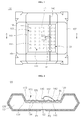
- FIG. 1 is a plan view showing a light emitting device package 100 according to a first embodiment
- FIG. 2 is a sectional view taken along line A-A of FIG. 1 .
- the light emitting device package 100 includes a package body 101, a first electrode 110, a second electrode 120, a nonconductive layer 130, a concave-convex structure 135, and a light emitting device 140.
- the package body 101 may include a conductive wafer such as a wafer level package (WLP) including silicon (Si).
- the package body 101 may include aluminum (Al), aluminum nitride (AlN), AlOx, photo sensitive glass (PSG), sapphire (Al 2 O 3 ), beryllium oxide (BeO), printed circuit board (PCB), or various resins, in addition to Si.
- Al aluminum
- AlN aluminum nitride
- AlOx aluminum oxide
- PSG photo sensitive glass
- Al 2 O 3 sapphire
- BeO beryllium oxide
- PCB printed circuit board
- the package body 101 may be etched through a bulk etching scheme as an etching process.
- a wet etching scheme, a dry etching scheme, and a laser drilling scheme may be used as the etching process. At least two among the etching schemes may be used together.
- a deep reactive ion etching scheme may be employed as the representative scheme of the dry etching scheme.
- a cavity 105 may be formed with a predetermined depth at an upper portion of the package body 101 through an etching process.
- the cavity 105 may include one of a bath tub shape recess, a polygonal recess, and a circular recess, but the embodiment is not limited thereto.
- the cavity may be formed by using wet etchants including anisotropic wet etchants such as a potassium hydroxide (KOH) solution, a Tetramethylammonium hydroxide (TMAH) solution, and an Ethylene Diamine Pyrochatechol (EDP) solution after a micro-pattern has been formed.
- KOH potassium hydroxide
- TMAH Tetramethylammonium hydroxide
- EDP Ethylene Diamine Pyrochatechol
- a lateral surface 103 of the cavity 105 in the package body 101 may be inclined at a predetermined angle or a predetermined curvature with respect to a cavity bottom surface, or may be vertically formed, but the embodiment is not limited thereto.
- An outer lateral surface 107 of the package body 101 may be inclined at a predetermined angle or may be vertically formed.
- the surface of the package body 101 is etched or cut at an angle according to the crystalline characteristic of a package body 101.
- the insulating layer 130 is formed on the surface of the package body 101.
- the insulating layer 130 may include one selected from the group consisting of silicon thermal oxides (e.g., SiO 2 and SixOy), aluminum oxide (e.g., AlOx), silicon nitrides (e.g., Si 3 N 4 , SixNy, and SiOxNy), alumina (e.g., AlN), and Al 2 O 3 .
- the insulating layer 130 insulates the package body 101 from the electrode layers 110 and 120.
- a plurality of protrusions 134 protrude from the insulating layer 130 provided on the bottom surface of the cavity 105, and the protrusions 134 protrude from the bottom surface of the cavity 105 and an opposite surface thereof while being spaced apart from each other.
- the protrusion 134 may have a side section having a lens shape, a hemispherical shape, or a dome shape.
- the protrusion 134 may have a diameter within the range of a few micrometers ( ⁇ m)(e.g. 0.1 ⁇ 9 ⁇ m), and have a height of a few micrometers ( ⁇ m) to a few tens micrometers ( ⁇ m)(e.g. 1 ⁇ 90 ⁇ m).
- the protrusion 134 have a height lower than a top surface of the light emitting device 140.
- the protrusions 134 may include a material the same as that of the insulating layer 130.
- a photoresist layer is coated through a photolithography process, and an exposure and development process is performed to pattern a selected region such that the selected region is exposed. Therefore, the selected region is formed in the structure of a protrusion.
- the protrusions 134 of the insulating layer 130 may be formed through another scheme. According to another scheme, after providing a photoresist layer, the protrusion 134 is formed or a wet etching scheme can be performed.
- the protrusions 134 may be formed at a regular interval or an irregular interval.
- the insulating layer 130 may be deposited through a sputtering scheme or an e-beam deposition scheme, but the embodiment is not limited thereto.
- At least one well may be formed in the package body 101, and the well may be formed in the package body 101 by implanting impurities or through a diffusion process.
- the well is connected to at least one of the electrodes 110 and 120 in the structure of a circuit, and may be realized by using a protective device such as a zener diode or a constant current device.
- a plurality of electrode layers 110 and 120 may be formed on the insulating layer 130.
- the electrode layers 110 and 120 may have a stack structure of a plurality of metallic layers based on thermal conductivity, electrical characteristics, light reflection efficiency, and the manufacturing process.
- the electrode layers 110 and 120 may be formed by coating a photoresist layer on a selected region and patterning the selected region through an exposure and development process such that the selected region is exposed, thereby forming metallic layers.
- the electrode layers 110 and 120 may be formed by performing a patterning process after the metallic layers have been formed, but the embodiment is not limited thereto.
- the first electrode layer 110 may be spaced apart from the second electrode layer 120.
- the first and second electrode layers 110 and 120 may be physically separated from each other by using a separator 145.
- the separator 145 may extend from an inner part of the cavity 105 to a top surface of the package body 110.
- the separator 145 may have the form of a groove and may include an insulating material.
- the separator 145 may have various structures or various shapes, but the embodiment is not limited thereto.
- the first and second electrode layers 110 and 120 may be formed on the insulating layer 130, or may extend to one side and an opposite side of the package body 101. In addition, the first and second electrode layers 110 and 120 may extend to both sides of a bottom surface of the package body 101.
- An end portion P1 of the first electrode layer 110 and an end portion P2 of the second electrode layer 120 may be used as electrode terminals.
- the light emitting device 140 may be provided in the cavity 105.
- the light emitting device 140 may be provided on the first electrode layer 110 and/or the second electrode layer 120.
- a structure in which the light emitting device 140 is provided on the first electrode layer 110 will be described as an example.
- the same number of metallic layers may be stacked at portions of the first and second electrode layers 110 and 120.
- a region of the first electrode layer 110, to which the light emitting device 140 is bonded, serves as a bonding region, and the remaining region of the first electrode layer 110 and the second electrode layer 120 serve as a reflective region.
- a reflective metallic layer may be additionally stacked in the reflective region provided inside and outside the cavity 105.
- the difference of the stack structure may be changed according to a bonding characteristic or a reflective characteristic.
- the light emitting device 140 may be provided on a flat top surface of the first electrode layer 110.
- the region in which the light emitting device 140 is provided may serve as a bonding region.
- the light emitting device 140 may be bonded to the bonding region by using a paste (not shown) or through a die attach scheme.
- the light emitting device 140 may include an LED chip such as a blue, green, red, or yellow LED chip having a visible wavelength, or may include an LED chip in an ultraviolet (UV) band, but the embodiment is not limited to the type or the number of the light emitting devices 140.
- the light emitting device 140 may be bonded onto the first electrode layer 110 and electrically connected to the first electrode layer 110, and may be connected to the second electrode layer 120 through a wire 142.
- the light emitting device 140 may include an LED chip having a vertical type electrode structure in which electrodes are vertically provided.
- An LED chip having a lateral type electrode structure may be connected to the first and second electrode layers 110 and 120 through a wire.
- the light emitting device 140 may employ at least one of a wire, a die bonding scheme, and a flip bonding scheme, but the embodiment is not limited thereto.
- the first electrode layer 110 and the second electrode layer 120 may include at least four metallic layers.
- the bonding region of the first electrode layer 110 may include at least five metallic layers
- the reflective region may include at least one metallic layer formed on the bonding region.
- the reflective region may be formed in a region onto which light is actually incident, and the bonding region may be formed in a region excluding the reflective region.
- the first and second electrode layers 110 and 120 may have a surface roughness of about 30 nm or less (e.g., 0.01 nm to 30 nm), and such a surface roughness can improve a conductive characteristic, a heat dissipation characteristic, and light reflection efficiency.
- the first and second electrode layers 110 and 120 have the concave-convex structure 135 by the protrusions 134 of the insulating layer 130.
- the concave-convex structure 135 is formed on the bottom surface of the cavity 105 excluding a chip mounting region in which the light emitting device 140 is mounted.
- the concave-convex structure 135 of the first and second electrode layers 110 and 120 is provided around the light emitting device 140 to scatter incident light, so that light efficiency can be improved.
- the concave-convex structure 135 includes a plurality of protrusions protruding from the electrode layers 110 and 120.
- a transmissive resin member 150 is formed in the cavity 105, and may have a single layer structure or a multiple layer structure.
- the transmissive resin member 150 seals or encapsulates the light emitting device 140, and includes resin such as silicon or epoxy.
- the transmissive resin member 150 may include at least one kind of phosphors, and the phosphors may include red, green, or yellow phosphors, but the embodiment is not limited thereof.
- the surface of the transmissive resin member 150 may have one of a concave shape, a flat shape, and convex shape.
- a lens may be formed on the cavity 105, and may include a convex lens shape, a concave lens shape, or the mixture of a convex lens shape and a concave lens shape on the transmissive resin member 150.
- the lens may be spaced apart from the transmissive resin member 150 or may make contact with the transmissive resin member 150, but the embodiment is not limited thereto.
- the lens may have various shapes, but the embodiment is not limited thereto.
- a fluorescent film including at least one kind of phosphor may be provided on the cavity 105, but the embodiment is not limited thereto.
- Silicon gel including phosphors or epoxy having superior permeability may be coated on a desired region of the transmissive resin member 150 or on a top surface of the transmissive resin member 150 through a screen printing scheme.
- the manufacturing process of the light emitting device package is as follows. After the insulating layer 130 and the first and second electrode layers 110 and 120 have been formed on the package body 101, the light emitting device 140 is electrically connected to the electrode layers 110 and 120. Then, the transmissive resin member 150 is formed in the cavity 105, and the package body 101 is cut in a package unit. The cut surface may be formed at a region excluding the first and second electrode layers 110 and 120.
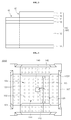
- FIG. 3 is a view showing a stack structure of the first and second electrode layers of FIG. 2 .
- the first and second electrode layers 110 and 120 include a seed layer 111, a conductive layer 112, a barrier layer 113, a bonding layer 114, an adhesion layer 116, and a reflective layer 117.
- a bonding region A1 has a structure in which the seed layer 111, the conductive layer 112, the barrier layer 113, and the bonding layer 114 are sequentially stacked
- the reflective region A2 has a structure in which the seed layer 111, the conductive layer 112, the barrier layer 113, the bonding layer 114, the adhesion layer 116, and the reflective layer 117 are sequentially stacked.
- the highest layer in the bonding region A1 is the bonding layer 114, and the bonding layer 114 may be formed at the bonding region of an LED chip and at the outer portion of a package.
- the bonding layer 114 is provided in the bonding region A1, the light emitting device 140 can adhere or be bonded. Since the uppermost layer of the reflective region A2 is the reflective layer 117, the electrode layers 110 and 120 may be provided in the cavity region or at an outer peripheral portion of the cavity region.
- the bonding layer 114 and the reflective layer 117 may have surface roughness of about 30 nm or less, and, preferably, may have surface roughness of about 20 nm or less.
- the surface roughness of the bonding layer 114 may be lower than the surface roughness of the reflective layer 117.
- the seed layer 111 is deposited through a physical deposition such as a sputtering scheme or an E-beam deposition scheme.
- the conductive layer 112, the barrier layer 113, the bonding layer 114, the adhesion layer 116, and the reflective layer 117 are formed through a plating scheme (electroplating or electroless-plating).
- the seed layer 111 includes a material having higher adhesive property with the insulating layer and higher bonding property with another metal.
- the seed layer 111 includes titanium (Ti), chromium (Cr), and tantalum (Ta) in a single layer structure or a multiple layer structure.
- the seed layer 111 may have a thickness of about 900 ⁇ ⁇ 200 ⁇ .
- the seed layer 111 is formed in the cavity 105 of the package body 101, on a top surface of the package body 101, at a lateral surface of the package body 101, and a bottom surface of the package body 101 to effectively dissipate heat emitted from the light emitting device 140.
- An intermediate seed layer may be further formed on the seed layer 111, and may include Au or Cu. Therefore, the seed layer 111 may have a structure of Cr/Au, Cr/Cu, Ti/Au, Ta/Cu, and Ta/Ti/Cu.
- the intermediate seed layer may have a thickness of about 600 nm ⁇ 50 nm (6000 ⁇ ⁇ 500 ⁇ ) through a physical deposition scheme.
- the conductive layer 112 is formed on the seed layer 111.
- the conductive layer 112 is formed through a plating scheme, and the plating scheme reduces stress with the seed layer 111 deposited through the physical deposition scheme.
- the stress reduction can prevent the surface roughness of the conductive layer 112 from being increased. In other words, the conductive layer 112 can prevent the stress occurring due to the difference in a formation method from the seed layer 111.
- the surface roughness of the conductive layer 112 is gradually reduced to a predetermined thickness in proportion to the thickness of a plated layer.
- the conductive layer 112 may include metal, such as Cu, having higher thermal conductivity and a heat dissipation characteristic.
- the conductive layer 112 may have a thickness of a few tens ⁇ m or less, or may have a thickness of about 30 ⁇ m or less.
- the conductive layer 112 may have a thickness of 10 ⁇ m or less.
- the conductive layer may have surface roughness of 20 nm or less. If the conductive layer 112 has a thickness of 10 ⁇ m to 30 ⁇ m, a heat dissipation characteristic and surface roughness can be improved.
- the conductive layer 112 may include materials such as silver (Ag), gold (Au), and aluminum (Al) in addition to copper (Cu).
- the conductive layer 112 may include Cu-alloy or Ag-alloy.
- the barrier layer 113 may be formed on the conductive layer 112.
- the barrier layer 113 prevents the electrical characteristic of the bonding layer 114 from being reduced due to the conductive layer 112 at a high temperature.
- the barrier layer 113 may be formed through a plating scheme using platinum (Pt) or nickel (Ni), and may have a thickness of about 300 nm ⁇ 50 nm (3000 ⁇ ⁇ 500 ⁇ ).
- the bonding layer 114 is formed on the barrier layer 113.
- the bonding layer 114 may be formed through a plating scheme using gold (Au), and has a thickness of about 500 nm ⁇ 50 nm (5000 ⁇ ⁇ 500 ⁇ ).
- the bonding layer 114 may have a surface roughness of about 30nm or less.
- the surface roughness of the bonding layer 114 can improve the bonding between the bonding layer 114 and the paste. As the surface roughness is increased, air is inflows into the bonded interfacial surface between the bonding layer 114 and the paste, so that thermal conductivity may be degraded. Accordingly, the surface roughness of 30 nm or less can improve the bonding property and thermal conductivity.
- the bonding region Al may have a stack structure of Cr/Au/Cu/Ni/Au, Cr/Cu/Cu/Ni/Au, Ti/Au/Cu/Ni/Au, Ta/Cu/Cu/Ni/Au, or Ta/Ti/Cu/Cu/Ni/Au.
- the conductive layer 112 is formed at a thickness of 10 ⁇ m or less, so that the surface roughness is lowered to 30 nm or less, and the thermal resistance of the metallic layer can be lowered.
- the adhesion layer 116 and the reflective layer 117 are stacked on the bonding layer 114.
- the adhesion layer 116 is formed to bond two adjacent metallic layers to each other, and may include titanium (Ti), chromium (Cr), or tantalum (Ta).
- the adhesion layer 116 may have a thickness of 90 nm ⁇ 10 nm (900 ⁇ ⁇ 100 ⁇ ). However, the adhesion layer 116 may not be formed.
- the reflective layer 117 is formed on the adhesion layer 116.
- the reflective layer 117 may include metal having superior reflectance to reflect light or alloy thereof.
- the reflective layer 117 may include Al, Ag, or alloy thereof.
- the reflective layer 117 is formed on the bottom surface and the lateral surface of the cavity 105 of FIG. 5 , so that light reflectance efficiency can be improved.
- the reflective layer 117 may have a thickness of about 150 nm ⁇ 30 nm (1500 ⁇ ⁇ 300 ⁇ ).
- the conductive layer 112 reduces stress transferred from the seed layer 111, so that the surface roughness of the bonding layer 114 and the reflective layer 117 formed on the conductive layer 112 may be 30 nm or less.
- the concave-convex structure is formed to at least one part of the seed layer 111, the conductive layer 112, the barrier layer 113, the bonding layer 114, the adhesion layer 116, and a reflective layer 117.
- FIG. 4 is a view showing a light emitting device package 100A according to a second embodiment.
- the second embodiment will be described with reference to FIG. 4 while focusing on the difference between the second embodiment and the first embodiment in order to avoid redundancy.
- the light emitting device package 100A includes the first concave-convex structure 135 formed at a bottom surface 102 of the cavity 105 in the package body 101, and a concave-convex structure 135A formed at a top surface 104 of the package body 101.
- a method of forming the first and second concave-convex structures 135 and 135A is considered with reference to the first embodiment.
- the first concave-convex structure 135 provided on the bottom surface of the cavity 105 scatters light emitted from the light emitting device 140 to improve light efficiency.
- the second concave-convex structure 135A provided on the top surface 104 of the package body 101 scatters light reflected by a lens, so that light extraction efficiency can be improved.
- FIGS. 5 and 6 are side sectional view showing the modified examples of a protrusion 134B of the insulating layer 130.
- the protrusion 134B of the insulating layer 130 may have a side section in a prism shape or a polygonal shape.
- the protrusion 134B may be formed through a photolithography process or a dry and/wet etching process by using the material of the insulating layer 130.
- the electrode layers 110 and 120 are formed on the insulating layer 130, thereby improving light reflection efficiency.
- a protrusion 134C of the insulating layer 130 may have a side section in a conical shape or a polygonal pyramid.
- the protrusion 134C may be formed through a photography process or a dry and/or wet etching process.
- the electrode layers 110 and 120 are formed on the insulating layer 130, thereby improving light reflective efficiency.
- Protrusions of the insulating layer 130 may have the same shape. Portions of the protrusions may have shapes different from each other, but the embodiment is not limited thereto.
- the cavity is not formed in the package body 101.
- the insulating layer and protrusions thereof are formed on the flat top surface, and the electrode layer may be formed on the insulating layer.
- a lighting system includes a light emitting module in which the light emitting device package of FIG. 1 is arrayed on a board in plurality.
- a light unit is provided to display apparatuses for portable terminals, notebook computers, etc., or is variously applicable to lighting apparatuses, indicator apparatuses, etc.
- the lighting system may include a display apparatus shown in FIGs. 7 and 8 , a light unit shown in FIG. 9 , in addition to a lighting lamp, a signal light, a vehicle headlight, an electronic display, etc.
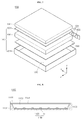
- FIG. 7 is a disassembled perspective view of a display apparatus according to an embodiment.
- the display apparatus 1000 may include a light guide panel 1041, a light emitting module 1031 supplying light to the light guide panel 1041, a reflective member 1022 under the light guide panel 1041, an optical sheet 1051 on the light guide panel 1041, a display panel 1061 on the optical sheet 1051, and a bottom cover 1011 receiving the light guide panel 1041, the light emitting module 1031, and the reflective member 1022, but the present invention is not limited thereto.
- the bottom cover 1011, the reflective sheet 1022, the light guide panel 1041, and the optical sheet 1051 may be defined as a light unit 1050.
- the light guide panel 1041 functions to transform linear light to planar light by diffusing the linear light.
- the light guide panel 1041 may be made of a transparent material, and may include one of acryl-series resin such as polymethyl metaacrylate (PMMA), polyethylene terephthlate (PET), poly carbonate (PC), Cyclic Olefin Copolymer (COC), and polyethylene naphthalate resin.
- PMMA polymethyl metaacrylate
- PET polyethylene terephthlate
- PC poly carbonate
- COC Cyclic Olefin Copolymer
- polyethylene naphthalate resin polyethylene naphthalate resin
- the light emitting module 1031 provides light to at least a side surface of the light guide panel 1041, and ultimately acts as a light source of a display apparatus.
- the light emitting module 1031 may include at least one light emitting device, and provide light directly or indirectly from one side surface of the light guide panel 1041.
- the light emitting module 1031 may include a board 1033, and a light emitting device package 100 according to embodiments disclosed above, and the light emitting device packages 100 may be arrayed apart by a predetermined interval from each other on the board 1033.
- the board 1033 may be a printed circuit board (PCB) including a circuit pattern (not shown).
- the board 1033 may include a metal core PCB (MCPCB), a flexible PCB (FPCB), etc. as well as the general PCB, but the present invention is not limited thereto.
- MCPCB metal core PCB
- FPCB flexible PCB
- the board 1033 may be removed.
- some of the heat releasing plate may contact an upper surface of the bottom cover 1011.
- the plurality of light emitting device packages 100 may be mounted on the board 1033 such that light emitting surfaces of the plurality of light emitting device packages 100 are spaced apart by a predetermined distance from the light guide panel 1041, but the present invention is not limited thereto.
- the light emitting device package 100 may supply light to a light incident part that is one side surface of the light guide panel 1041, directly or indirectly, but the present invention is not limited thereto.
- the reflective member 1022 may be provided under the light guide panel 1041.
- the reflective member 1022 reflects light incident from a lower surface of the light guide panel 1041 to allow the reflected light to be directed toward an upper direction, thereby capable of enhancing brightness of the light unit 1050.
- the reflective member 1022 may be formed of, for example, polyethylene terephthalate (PET), polycarbonate (PC), polyvinyl chloride (PVC) resin, or the like, but the present invention is not limited thereto.
- the bottom cover 1011 may receive the light guide panel 1041, the light emitting module 1031, the reflective member 1022, and the like.
- the bottom cover 1011 may have a receiving part 1012 formed in a box shape a top surface of which is opened, but the present invention is not limited thereto.
- the bottom cover 1011 may be coupled to a top cover, but the present invention is not limited thereto.
- the bottom cover 1011 may be formed of a metal material or resin material, and may be manufactured by using a process such as a press molding or an injection molding. Also, the bottom cover 1011 may include metallic or nonmetallic material having a high thermal conductivity, but the present invention is not limited thereto.
- the display panel 1061 is, for example, an LCD panel, and includes first and second transparent substrates facing each other, and a liquid crystal layer interposed between the first and second substrates.
- a polarizing plate may be attached over at least one surface of the display panel 1061, but the present invention is not limited thereto.
- the display panel 1061 displays information by using light passing through the optical sheet 1051.
- the display apparatus 1000 may be applied to a variety of mobile terminals, monitors for notebook computers, monitors for lap-top computers, televisions, etc.
- the optical sheet 1051 is disposed between the display panel 1061 and the light guide panel 1041, and includes at least one transparent sheet.
- the optical sheet 1051 may include, for example, at least one of a diffusion sheet, a horizontal and/or vertical prism sheet, and a brightness reinforcing sheet.
- the diffusion sheet diffuses incident light
- the horizontal and/or vertical prism sheet focuses incident light on a display region
- the brightness reinforcing sheet enhances the brightness by reusing lost light.
- a protective sheet may be disposed on the display panel 1061, but the present invention is not limited thereto.
- the display apparatus 1000 may include the light guide panel 1041 and the optical sheet 1051 as optical members positioned on a light path of the light emitting module 1031, but the present invention is not limited thereto.
- FIG. 8 is a cross-sectional view of a display apparatus according to an embodiment.
- the display apparatus 1100 includes a bottom cover 1152, a board 1120 on which the light emitting device packages 100 disclosed above are arrayed, an optical member 1154, and a display panel 1155.
- the board 1120 and the light emitting device package 100 may be defined as a light emitting module 1060.
- the bottom cover 1152, the at least one light emitting module 1060, and the optical member 1154 may be defined as a light unit 1150.
- the bottom cover 1152 may be provided with a receiving part 1153, but the present invention is not limited thereto.
- the optical member 1154 may include at least one of a lens, a light guide panel, a diffusion sheet, a horizontal and vertical prism sheet, and a brightness reinforcing sheet.
- the light guide panel may be formed of polycarbonate (PC) or poly methyl methacrylate (PMMA), and may be removed.
- the diffusion sheet diffuses incident light
- the horizontal and vertical prism sheet focuses incident light on a display region
- the brightness reinforcing sheet enhances the brightness by reusing lost light.
- the optical member 1154 is disposed on the light emitting module 1060.
- the optical member 1154 transforms light emitted from the light emitting module 1060 to planar light, and performs diffusion, light focusing, and the like.
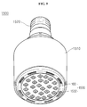
- FIG. 9 is a perspective view of a lighting unit according to an embodiment.
- the lighting unit 1500 may include a case 1510, a light emitting module 1530 equipped in the case 1510, and a connection terminal 1520 equipped in the case 1510 and supplied with an electric power from an external power supply.
- the case 1510 may be preferably formed of a material having good heat shielding characteristics, for example, a metal material or a resin material.
- the light emitting module 1530 may include a board 1532, and at least one light emitting device package 100 according to the embodiments mounted on the board 1532.
- the light emitting device package 100 may include a plurality of light emitting device packages which are arrayed apart by a predetermined distance from one another in a matrix configuration.
- the board 1532 may be an insulator substrate on which a circuit pattern is printed, and may include, for example, a general printed circuit board (PCB), a metal core PCB, a flexible PCB, a ceramic PCB, an FR-4 substrate, etc.
- PCB general printed circuit board
- the board 1532 may be formed of a material to efficiently reflect light, and a surface thereof may be formed in a color capable of efficiently reflecting light, for example, white color, or silver color.
- the at least one light emitting device packages 100 may be mounted on the board 1532.
- Each of the light emitting device packages 100 may include at least one light emitting diode (LED) chip.
- the LED chip may include a color LED emitting red, green, blue or white light, and a UV LED emitting ultraviolet (UV).
- the light emitting module 1530 may have a combination of various light emitting device packages so as to obtain desired color and luminance.
- the light emitting module 1530 may have a combination of a white LED, a red LED, and a green LED so as to obtain a high color rendering index (CRI).
- CRI color rendering index
- connection terminal 1520 may be electrically connected to the light emitting module 1530 to supply power.
- the connection terminal 1520 may be screwed and coupled to an external power in a socket type, but the present invention is not limited thereto.
- the connection terminal 1520 may be made in a pin type and inserted into an external power, or may be connected to the external power through a power line.
- a light emitting module of a light unit includes the light emitting device package.
- the light emitting device package may have the above disclosed package structure.
- the resultant structure is packaged by using a molding member.
- a method of manufacturing a light emitting device package includes steps of forming an insulating layer on a surface of a package body, forming a plurality of protrusions in a first region of the insulating layer, forming a plurality of metallic layers on the insulating layer, and connecting the light emitting device with the metallic layers.
Landscapes
- Led Device Packages (AREA)
Description
- The embodiment relates to a light emitting device package and a light unit having the same.
- A light emitting diode (LED) is a semiconductor light emitting device that converts current into light. Recently, the brightness of the LED has increased, so that the LED has been employed as a light source for a display device, a vehicle, or a lighting device. In addition, the LED can represent a white color having superior light efficiency by employing phosphors or combining LEDs having various colors.
- Documents
WO 2009/014376 andEP 1 816 686 disclose relevant prior art. - In order to increase the brightness and the performance of the LED, a light extraction structure, the structure of an active layer, current diffusion, the structure of an electrode, and the structure of a light emitting diode package have been improved.
- The embodiment provides a light emitting device package having improved light efficiency and a light unit having the same. The embodiment provides a light emitting device package including a plurality of protrusions on a body including a conductive material and a light unit having the same.
- The embodiment provides a light emitting device package including a plurality of protrusions protruding from a nonconductive layer, electrodes, and a light unit having the same.
- The embodiment provides a light emitting device package having improved reliability and a light unit package body, a plurality of electrodes on the nonconductive layer, a plurality of protrusions protruding from the electrodes, a light emitting device mounted to a plane of the package body and connected to the electrodes, and a transmissive resin member to encapsulate the light emitting device, wherein at least the plane of the package body other than where the light emitting device is seated is substantially flat.
- According to the embodiment, a light emitting device package includes a package body including a cavity, in which a top portion is opened, and a conductive material, a nonconductive layer on a surface of the package body, and including a plurality of protrusions in the cavity, a plurality of electrodes on the nonconductive layer that follow a contour of the protrusions, and a light emitting device provided in the cavity and connected to the electrodes, wherein at least a bottom surface of the cavity other than where the light emitting device is seated is substantially flat.
- According to the embodiment, a light unit includes a plurality of light emitting device packages, a substrate arranged in the light emitting device packages, an optical member provided at one side of the substrate and including at least one of a light guide plate and an optical sheet, and a cover covering outer peripheral portions of the substrate and the optical member wherein the light emitting device package includes a package body including a conductive material, a nonconductive layer on a surface of the package body, a plurality of electrodes on the nonconductive layer, a plurality of protrusions from the electrodes, a light emitting device connected to the electrodes, and a transmissive resin member to encapsulate the light emitting device.
- The invention discloses a light emitting structure according to claim 1.
-
-
FIG. 1 is a plan view showing a light emitting device package according to a first embodiment; -
FIG. 2 is a side sectional view showing the light emitting device package ofFIG. 1 ; -
FIG. 3 is a detailed sectional view showing an electrode layer ofFIG. 2 ; -
FIG. 4 is a plan view showing a light emitting device package according to a second embodiment; -
FIG. 5 is a side sectional view showing the modified protrusion according to an embodiment; and -
FIG. 6 is a side sectional view showing the modified protrusion according to an embodiment. -
FIG. 7 is a disassembled perspective view of a display apparatus provided with the light emitting device package ofFIG. 1 . -
FIG. 8 is a schematic sectional view illustrating another example of a display apparatus provided with the light emitting device package ofFIG. 1 . -
FIG. 9 is a perspective view of a lighting apparatus provided with the light emitting device package ofFIG. 1 . - In the description of the embodiments, it will be understood that, when a layer (or film), a region, a pattern, or a structure is referred to as being "on" or "under" another substrate, another layer (or film), another region, another pad, or another pattern, it can be "directly" or "indirectly" on the other substrate, layer (or film), region, pad, or pattern, or one or more intervening layers may also be present. Such a position of the layer has been described with reference to the drawings.
- Hereinafter, the embodiment will be described with reference to accompanying drawings. The thickness and size of each layer shown in the drawings may be exaggerated, omitted or schematically drawn for the purpose of convenience or clarity. In addition, the size of elements does not utterly reflect an actual size.
-
FIG. 1 is a plan view showing a lightemitting device package 100 according to a first embodiment, andFIG. 2 is a sectional view taken along line A-A ofFIG. 1 . - Referring to
FIGS. 1 and 2 , the lightemitting device package 100 includes apackage body 101, afirst electrode 110, asecond electrode 120, anonconductive layer 130, a concave-convex structure 135, and alight emitting device 140. - The
package body 101 may include a conductive wafer such as a wafer level package (WLP) including silicon (Si). Thepackage body 101 may include aluminum (Al), aluminum nitride (AlN), AlOx, photo sensitive glass (PSG), sapphire (Al2O3), beryllium oxide (BeO), printed circuit board (PCB), or various resins, in addition to Si. Hereinafter, according to the embodiment, description will be made regarding a case in which thepackage body 101 includes Si representing superior performance in the manufacturing efficiency and heat dissipation efficiency of the light emitting device package. - The
package body 101 may be etched through a bulk etching scheme as an etching process. In addition, as the etching process, a wet etching scheme, a dry etching scheme, and a laser drilling scheme may be used. At least two among the etching schemes may be used together. A deep reactive ion etching scheme may be employed as the representative scheme of the dry etching scheme. - A
cavity 105 may be formed with a predetermined depth at an upper portion of thepackage body 101 through an etching process. Thecavity 105 may include one of a bath tub shape recess, a polygonal recess, and a circular recess, but the embodiment is not limited thereto. The cavity may be formed by using wet etchants including anisotropic wet etchants such as a potassium hydroxide (KOH) solution, a Tetramethylammonium hydroxide (TMAH) solution, and an Ethylene Diamine Pyrochatechol (EDP) solution after a micro-pattern has been formed. Thecavity 105 may not be formed. - A
lateral surface 103 of thecavity 105 in thepackage body 101 may be inclined at a predetermined angle or a predetermined curvature with respect to a cavity bottom surface, or may be vertically formed, but the embodiment is not limited thereto. An outerlateral surface 107 of thepackage body 101 may be inclined at a predetermined angle or may be vertically formed. The surface of thepackage body 101 is etched or cut at an angle according to the crystalline characteristic of apackage body 101. - The
insulating layer 130 is formed on the surface of thepackage body 101. For example, theinsulating layer 130 may include one selected from the group consisting of silicon thermal oxides (e.g., SiO2 and SixOy), aluminum oxide (e.g., AlOx), silicon nitrides (e.g., Si3N4, SixNy, and SiOxNy), alumina (e.g., AlN), and Al2O3. - The
insulating layer 130 insulates thepackage body 101 from theelectrode layers - A plurality of
protrusions 134 protrude from theinsulating layer 130 provided on the bottom surface of thecavity 105, and theprotrusions 134 protrude from the bottom surface of thecavity 105 and an opposite surface thereof while being spaced apart from each other. - The
protrusion 134 may have a side section having a lens shape, a hemispherical shape, or a dome shape. Theprotrusion 134 may have a diameter within the range of a few micrometers (µm)(e.g. 0.1∼9 µm), and have a height of a few micrometers (µm) to a few tens micrometers (µm)(e.g. 1∼90 µm). In addition, theprotrusion 134 have a height lower than a top surface of thelight emitting device 140. - The
protrusions 134 may include a material the same as that of theinsulating layer 130. In order to form theprotrusions 134 from theinsulating layer 130, after forming theinsulating layer 130 at a predetermined thickness, a photoresist layer is coated through a photolithography process, and an exposure and development process is performed to pattern a selected region such that the selected region is exposed. Therefore, the selected region is formed in the structure of a protrusion. Theprotrusions 134 of theinsulating layer 130 may be formed through another scheme. According to another scheme, after providing a photoresist layer, theprotrusion 134 is formed or a wet etching scheme can be performed. Theprotrusions 134 may be formed at a regular interval or an irregular interval. - The
insulating layer 130 may be deposited through a sputtering scheme or an e-beam deposition scheme, but the embodiment is not limited thereto. - At least one well may be formed in the
package body 101, and the well may be formed in thepackage body 101 by implanting impurities or through a diffusion process. The well is connected to at least one of theelectrodes - A plurality of
electrode layers insulating layer 130. Hereinafter, according to the embodiment, a structure in which theelectrode layers - The electrode layers 110 and 120 may be formed by coating a photoresist layer on a selected region and patterning the selected region through an exposure and development process such that the selected region is exposed, thereby forming metallic layers. In addition, the electrode layers 110 and 120 may be formed by performing a patterning process after the metallic layers have been formed, but the embodiment is not limited thereto.
- The
first electrode layer 110 may be spaced apart from thesecond electrode layer 120. The first and second electrode layers 110 and 120 may be physically separated from each other by using aseparator 145. Theseparator 145 may extend from an inner part of thecavity 105 to a top surface of thepackage body 110. Theseparator 145 may have the form of a groove and may include an insulating material. Theseparator 145 may have various structures or various shapes, but the embodiment is not limited thereto. - The first and second electrode layers 110 and 120 may be formed on the insulating
layer 130, or may extend to one side and an opposite side of thepackage body 101. In addition, the first and second electrode layers 110 and 120 may extend to both sides of a bottom surface of thepackage body 101. - An end portion P1 of the
first electrode layer 110 and an end portion P2 of thesecond electrode layer 120 may be used as electrode terminals. - The
light emitting device 140 may be provided in thecavity 105. Thelight emitting device 140 may be provided on thefirst electrode layer 110 and/or thesecond electrode layer 120. Hereinafter, for the purpose of explanation, a structure in which thelight emitting device 140 is provided on thefirst electrode layer 110 will be described as an example. - The same number of metallic layers may be stacked at portions of the first and second electrode layers 110 and 120. A region of the
first electrode layer 110, to which thelight emitting device 140 is bonded, serves as a bonding region, and the remaining region of thefirst electrode layer 110 and thesecond electrode layer 120 serve as a reflective region. - A reflective metallic layer may be additionally stacked in the reflective region provided inside and outside the
cavity 105. The difference of the stack structure may be changed according to a bonding characteristic or a reflective characteristic. - The
light emitting device 140 may be provided on a flat top surface of thefirst electrode layer 110. The region in which thelight emitting device 140 is provided may serve as a bonding region. Thelight emitting device 140 may be bonded to the bonding region by using a paste (not shown) or through a die attach scheme. Thelight emitting device 140 may include an LED chip such as a blue, green, red, or yellow LED chip having a visible wavelength, or may include an LED chip in an ultraviolet (UV) band, but the embodiment is not limited to the type or the number of thelight emitting devices 140. - The
light emitting device 140 may be bonded onto thefirst electrode layer 110 and electrically connected to thefirst electrode layer 110, and may be connected to thesecond electrode layer 120 through awire 142. According to the embodiment, thelight emitting device 140 may include an LED chip having a vertical type electrode structure in which electrodes are vertically provided. An LED chip having a lateral type electrode structure may be connected to the first and second electrode layers 110 and 120 through a wire. Thelight emitting device 140 may employ at least one of a wire, a die bonding scheme, and a flip bonding scheme, but the embodiment is not limited thereto. - The
first electrode layer 110 and thesecond electrode layer 120 may include at least four metallic layers. For example, the bonding region of thefirst electrode layer 110 may include at least five metallic layers, and the reflective region may include at least one metallic layer formed on the bonding region. The reflective region may be formed in a region onto which light is actually incident, and the bonding region may be formed in a region excluding the reflective region. - The first and second electrode layers 110 and 120 may have a surface roughness of about 30 nm or less (e.g., 0.01 nm to 30 nm), and such a surface roughness can improve a conductive characteristic, a heat dissipation characteristic, and light reflection efficiency.
- Referring to
FIG. 1 , the first and second electrode layers 110 and 120 have the concave-convex structure 135 by theprotrusions 134 of the insulatinglayer 130. The concave-convex structure 135 is formed on the bottom surface of thecavity 105 excluding a chip mounting region in which thelight emitting device 140 is mounted. The concave-convex structure 135 of the first and second electrode layers 110 and 120 is provided around thelight emitting device 140 to scatter incident light, so that light efficiency can be improved. The concave-convex structure 135 includes a plurality of protrusions protruding from the electrode layers 110 and 120. - Referring to
FIG. 2 , atransmissive resin member 150 is formed in thecavity 105, and may have a single layer structure or a multiple layer structure. Thetransmissive resin member 150 seals or encapsulates thelight emitting device 140, and includes resin such as silicon or epoxy. Thetransmissive resin member 150 may include at least one kind of phosphors, and the phosphors may include red, green, or yellow phosphors, but the embodiment is not limited thereof. The surface of thetransmissive resin member 150 may have one of a concave shape, a flat shape, and convex shape. - A lens (not shown) may be formed on the
cavity 105, and may include a convex lens shape, a concave lens shape, or the mixture of a convex lens shape and a concave lens shape on thetransmissive resin member 150. The lens may be spaced apart from thetransmissive resin member 150 or may make contact with thetransmissive resin member 150, but the embodiment is not limited thereto. The lens may have various shapes, but the embodiment is not limited thereto. - A fluorescent film including at least one kind of phosphor may be provided on the
cavity 105, but the embodiment is not limited thereto. Silicon gel including phosphors or epoxy having superior permeability may be coated on a desired region of thetransmissive resin member 150 or on a top surface of thetransmissive resin member 150 through a screen printing scheme. - The manufacturing process of the light emitting device package is as follows. After the insulating
layer 130 and the first and second electrode layers 110 and 120 have been formed on thepackage body 101, thelight emitting device 140 is electrically connected to the electrode layers 110 and 120. Then, thetransmissive resin member 150 is formed in thecavity 105, and thepackage body 101 is cut in a package unit. The cut surface may be formed at a region excluding the first and second electrode layers 110 and 120. -
FIG. 3 is a view showing a stack structure of the first and second electrode layers ofFIG. 2 . - Referring to
FIGS. 2 and3 , the first and second electrode layers 110 and 120 include aseed layer 111, aconductive layer 112, abarrier layer 113, abonding layer 114, anadhesion layer 116, and areflective layer 117. - A bonding region A1 has a structure in which the
seed layer 111, theconductive layer 112, thebarrier layer 113, and thebonding layer 114 are sequentially stacked, and the reflective region A2 has a structure in which theseed layer 111, theconductive layer 112, thebarrier layer 113, thebonding layer 114, theadhesion layer 116, and thereflective layer 117 are sequentially stacked. The highest layer in the bonding region A1 is thebonding layer 114, and thebonding layer 114 may be formed at the bonding region of an LED chip and at the outer portion of a package. - Since the
bonding layer 114 is provided in the bonding region A1, thelight emitting device 140 can adhere or be bonded. Since the uppermost layer of the reflective region A2 is thereflective layer 117, the electrode layers 110 and 120 may be provided in the cavity region or at an outer peripheral portion of the cavity region. - The
bonding layer 114 and thereflective layer 117 may have surface roughness of about 30 nm or less, and, preferably, may have surface roughness of about 20 nm or less. The surface roughness of thebonding layer 114 may be lower than the surface roughness of thereflective layer 117. - The
seed layer 111 is deposited through a physical deposition such as a sputtering scheme or an E-beam deposition scheme. Theconductive layer 112, thebarrier layer 113, thebonding layer 114, theadhesion layer 116, and thereflective layer 117 are formed through a plating scheme (electroplating or electroless-plating). Theseed layer 111 includes a material having higher adhesive property with the insulating layer and higher bonding property with another metal. For example, theseed layer 111 includes titanium (Ti), chromium (Cr), and tantalum (Ta) in a single layer structure or a multiple layer structure. Theseed layer 111 may have a thickness of about 900 Å ± 200 Å. - The
seed layer 111 is formed in thecavity 105 of thepackage body 101, on a top surface of thepackage body 101, at a lateral surface of thepackage body 101, and a bottom surface of thepackage body 101 to effectively dissipate heat emitted from thelight emitting device 140. - An intermediate seed layer may be further formed on the
seed layer 111, and may include Au or Cu. Therefore, theseed layer 111 may have a structure of Cr/Au, Cr/Cu, Ti/Au, Ta/Cu, and Ta/Ti/Cu. The intermediate seed layer may have a thickness of about 600 nm ± 50 nm (6000Å ± 500 Å) through a physical deposition scheme. - The
conductive layer 112 is formed on theseed layer 111. Theconductive layer 112 is formed through a plating scheme, and the plating scheme reduces stress with theseed layer 111 deposited through the physical deposition scheme. The stress reduction can prevent the surface roughness of theconductive layer 112 from being increased. In other words, theconductive layer 112 can prevent the stress occurring due to the difference in a formation method from theseed layer 111. - The surface roughness of the
conductive layer 112 is gradually reduced to a predetermined thickness in proportion to the thickness of a plated layer. Theconductive layer 112 may include metal, such as Cu, having higher thermal conductivity and a heat dissipation characteristic. Theconductive layer 112 may have a thickness of a few tens µm or less, or may have a thickness of about 30 µm or less. Preferably, theconductive layer 112 may have a thickness of 10 µm or less. When theconductive layer 112 has a thickness of a few micrometers (µm), the conductive layer may have surface roughness of 20 nm or less. If theconductive layer 112 has a thickness of 10 µm to 30 µm, a heat dissipation characteristic and surface roughness can be improved. - The
conductive layer 112 may include materials such as silver (Ag), gold (Au), and aluminum (Al) in addition to copper (Cu). Theconductive layer 112 may include Cu-alloy or Ag-alloy. - The
barrier layer 113 may be formed on theconductive layer 112. Thebarrier layer 113 prevents the electrical characteristic of thebonding layer 114 from being reduced due to theconductive layer 112 at a high temperature. Thebarrier layer 113 may be formed through a plating scheme using platinum (Pt) or nickel (Ni), and may have a thickness of about 300 nm ± 50 nm (3000Å ± 500 Å). - The
bonding layer 114 is formed on thebarrier layer 113. Thebonding layer 114 may be formed through a plating scheme using gold (Au), and has a thickness of about 500 nm ± 50 nm (5000 Å ± 500 Å). - The
bonding layer 114 may have a surface roughness of about 30nm or less. The surface roughness of thebonding layer 114 can improve the bonding between thebonding layer 114 and the paste. As the surface roughness is increased, air is inflows into the bonded interfacial surface between thebonding layer 114 and the paste, so that thermal conductivity may be degraded. Accordingly, the surface roughness of 30 nm or less can improve the bonding property and thermal conductivity. - When the
conductive layer 112 includes Cu, thebarrier layer 113 includes Ni, and thebonding layer 114 includes Au, the bonding region Al may have a stack structure of Cr/Au/Cu/Ni/Au, Cr/Cu/Cu/Ni/Au, Ti/Au/Cu/Ni/Au, Ta/Cu/Cu/Ni/Au, or Ta/Ti/Cu/Cu/Ni/Au. In the stack structure, theconductive layer 112 is formed at a thickness of 10 µm or less, so that the surface roughness is lowered to 30 nm or less, and the thermal resistance of the metallic layer can be lowered. - The
adhesion layer 116 and thereflective layer 117 are stacked on thebonding layer 114. Theadhesion layer 116 is formed to bond two adjacent metallic layers to each other, and may include titanium (Ti), chromium (Cr), or tantalum (Ta). Theadhesion layer 116 may have a thickness of 90 nm ± 10 nm (900 Å ± 100 Å). However, theadhesion layer 116 may not be formed. - The
reflective layer 117 is formed on theadhesion layer 116. Thereflective layer 117 may include metal having superior reflectance to reflect light or alloy thereof. For example, thereflective layer 117 may include Al, Ag, or alloy thereof. Thereflective layer 117 is formed on the bottom surface and the lateral surface of thecavity 105 ofFIG. 5 , so that light reflectance efficiency can be improved. Thereflective layer 117 may have a thickness of about 150 nm ± 30 nm (1500 Å ± 300 Å). - The
conductive layer 112 reduces stress transferred from theseed layer 111, so that the surface roughness of thebonding layer 114 and thereflective layer 117 formed on theconductive layer 112 may be 30 nm or less. - The concave-convex structure is formed to at least one part of the
seed layer 111, theconductive layer 112, thebarrier layer 113, thebonding layer 114, theadhesion layer 116, and areflective layer 117. -
FIG. 4 is a view showing a light emittingdevice package 100A according to a second embodiment. Hereinafter, the second embodiment will be described with reference toFIG. 4 while focusing on the difference between the second embodiment and the first embodiment in order to avoid redundancy. - Referring to
FIG. 4 , the light emittingdevice package 100A includes the first concave-convex structure 135 formed at abottom surface 102 of thecavity 105 in thepackage body 101, and a concave-convex structure 135A formed at a top surface 104 of thepackage body 101. - A method of forming the first and second concave-
convex structures convex structure 135 provided on the bottom surface of thecavity 105 scatters light emitted from thelight emitting device 140 to improve light efficiency. The second concave-convex structure 135A provided on the top surface 104 of thepackage body 101 scatters light reflected by a lens, so that light extraction efficiency can be improved. -
FIGS. 5 and 6 are side sectional view showing the modified examples of aprotrusion 134B of the insulatinglayer 130. - Referring to
FIG. 5 , theprotrusion 134B of the insulatinglayer 130 may have a side section in a prism shape or a polygonal shape. Theprotrusion 134B may be formed through a photolithography process or a dry and/wet etching process by using the material of the insulatinglayer 130. The electrode layers 110 and 120 are formed on the insulatinglayer 130, thereby improving light reflection efficiency. - Referring to
FIG. 6 , aprotrusion 134C of the insulatinglayer 130 may have a side section in a conical shape or a polygonal pyramid. Theprotrusion 134C may be formed through a photography process or a dry and/or wet etching process. The electrode layers 110 and 120 are formed on the insulatinglayer 130, thereby improving light reflective efficiency. - Protrusions of the insulating
layer 130 may have the same shape. Portions of the protrusions may have shapes different from each other, but the embodiment is not limited thereto. - According to the embodiment, the cavity is not formed in the
package body 101. In this case, the insulating layer and protrusions thereof are formed on the flat top surface, and the electrode layer may be formed on the insulating layer. - A lighting system according to an embodiment includes a light emitting module in which the light emitting device package of
FIG. 1 is arrayed on a board in plurality. In the lighting system, a light unit is provided to display apparatuses for portable terminals, notebook computers, etc., or is variously applicable to lighting apparatuses, indicator apparatuses, etc. - The lighting system may include a display apparatus shown in
FIGs. 7 and 8 , a light unit shown inFIG. 9 , in addition to a lighting lamp, a signal light, a vehicle headlight, an electronic display, etc. -
FIG. 7 is a disassembled perspective view of a display apparatus according to an embodiment. - Referring to
FIG. 7 , thedisplay apparatus 1000 according to the embodiment may include alight guide panel 1041, alight emitting module 1031 supplying light to thelight guide panel 1041, areflective member 1022 under thelight guide panel 1041, anoptical sheet 1051 on thelight guide panel 1041, adisplay panel 1061 on theoptical sheet 1051, and abottom cover 1011 receiving thelight guide panel 1041, thelight emitting module 1031, and thereflective member 1022, but the present invention is not limited thereto. - The
bottom cover 1011, thereflective sheet 1022, thelight guide panel 1041, and theoptical sheet 1051 may be defined as alight unit 1050. - The
light guide panel 1041 functions to transform linear light to planar light by diffusing the linear light. Thelight guide panel 1041 may be made of a transparent material, and may include one of acryl-series resin such as polymethyl metaacrylate (PMMA), polyethylene terephthlate (PET), poly carbonate (PC), Cyclic Olefin Copolymer (COC), and polyethylene naphthalate resin. - The
light emitting module 1031 provides light to at least a side surface of thelight guide panel 1041, and ultimately acts as a light source of a display apparatus. - The
light emitting module 1031 may include at least one light emitting device, and provide light directly or indirectly from one side surface of thelight guide panel 1041. Thelight emitting module 1031 may include aboard 1033, and a light emittingdevice package 100 according to embodiments disclosed above, and the light emitting device packages 100 may be arrayed apart by a predetermined interval from each other on theboard 1033. - The
board 1033 may be a printed circuit board (PCB) including a circuit pattern (not shown). Theboard 1033 may include a metal core PCB (MCPCB), a flexible PCB (FPCB), etc. as well as the general PCB, but the present invention is not limited thereto. In the case where the light emittingdevice package 100 is mounted on a side surface or a heat releasing plate, theboard 1033 may be removed. Herein, some of the heat releasing plate may contact an upper surface of thebottom cover 1011. - The plurality of light emitting device packages 100 may be mounted on the
board 1033 such that light emitting surfaces of the plurality of light emitting device packages 100 are spaced apart by a predetermined distance from thelight guide panel 1041, but the present invention is not limited thereto. The light emittingdevice package 100 may supply light to a light incident part that is one side surface of thelight guide panel 1041, directly or indirectly, but the present invention is not limited thereto. - The
reflective member 1022 may be provided under thelight guide panel 1041. Thereflective member 1022 reflects light incident from a lower surface of thelight guide panel 1041 to allow the reflected light to be directed toward an upper direction, thereby capable of enhancing brightness of thelight unit 1050. Thereflective member 1022 may be formed of, for example, polyethylene terephthalate (PET), polycarbonate (PC), polyvinyl chloride (PVC) resin, or the like, but the present invention is not limited thereto. - The
bottom cover 1011 may receive thelight guide panel 1041, thelight emitting module 1031, thereflective member 1022, and the like. For this purpose, thebottom cover 1011 may have a receivingpart 1012 formed in a box shape a top surface of which is opened, but the present invention is not limited thereto. Thebottom cover 1011 may be coupled to a top cover, but the present invention is not limited thereto. - The
bottom cover 1011 may be formed of a metal material or resin material, and may be manufactured by using a process such as a press molding or an injection molding. Also, thebottom cover 1011 may include metallic or nonmetallic material having a high thermal conductivity, but the present invention is not limited thereto. - The
display panel 1061 is, for example, an LCD panel, and includes first and second transparent substrates facing each other, and a liquid crystal layer interposed between the first and second substrates. A polarizing plate may be attached over at least one surface of thedisplay panel 1061, but the present invention is not limited thereto. Thedisplay panel 1061 displays information by using light passing through theoptical sheet 1051. Thedisplay apparatus 1000 may be applied to a variety of mobile terminals, monitors for notebook computers, monitors for lap-top computers, televisions, etc. - The
optical sheet 1051 is disposed between thedisplay panel 1061 and thelight guide panel 1041, and includes at least one transparent sheet. Theoptical sheet 1051 may include, for example, at least one of a diffusion sheet, a horizontal and/or vertical prism sheet, and a brightness reinforcing sheet. The diffusion sheet diffuses incident light, the horizontal and/or vertical prism sheet focuses incident light on a display region, and the brightness reinforcing sheet enhances the brightness by reusing lost light. Also, a protective sheet may be disposed on thedisplay panel 1061, but the present invention is not limited thereto. - Herein, the
display apparatus 1000 may include thelight guide panel 1041 and theoptical sheet 1051 as optical members positioned on a light path of thelight emitting module 1031, but the present invention is not limited thereto. -
FIG. 8 is a cross-sectional view of a display apparatus according to an embodiment. - Referring to
FIG. 8 , thedisplay apparatus 1100 includes abottom cover 1152, aboard 1120 on which the light emitting device packages 100 disclosed above are arrayed, anoptical member 1154, and adisplay panel 1155. - The
board 1120 and the light emittingdevice package 100 may be defined as a light emitting module 1060. Thebottom cover 1152, the at least one light emitting module 1060, and theoptical member 1154 may be defined as alight unit 1150. - The
bottom cover 1152 may be provided with a receivingpart 1153, but the present invention is not limited thereto. - Herein, the
optical member 1154 may include at least one of a lens, a light guide panel, a diffusion sheet, a horizontal and vertical prism sheet, and a brightness reinforcing sheet. The light guide panel may be formed of polycarbonate (PC) or poly methyl methacrylate (PMMA), and may be removed. The diffusion sheet diffuses incident light, the horizontal and vertical prism sheet focuses incident light on a display region, and the brightness reinforcing sheet enhances the brightness by reusing lost light. - The
optical member 1154 is disposed on the light emitting module 1060. Theoptical member 1154 transforms light emitted from the light emitting module 1060 to planar light, and performs diffusion, light focusing, and the like. -
FIG. 9 is a perspective view of a lighting unit according to an embodiment. - Referring to
FIG. 9 , thelighting unit 1500 may include acase 1510, alight emitting module 1530 equipped in thecase 1510, and aconnection terminal 1520 equipped in thecase 1510 and supplied with an electric power from an external power supply. - The
case 1510 may be preferably formed of a material having good heat shielding characteristics, for example, a metal material or a resin material. - The
light emitting module 1530 may include aboard 1532, and at least one light emittingdevice package 100 according to the embodiments mounted on theboard 1532. The light emittingdevice package 100 may include a plurality of light emitting device packages which are arrayed apart by a predetermined distance from one another in a matrix configuration. - The
board 1532 may be an insulator substrate on which a circuit pattern is printed, and may include, for example, a general printed circuit board (PCB), a metal core PCB, a flexible PCB, a ceramic PCB, an FR-4 substrate, etc. - Also, the
board 1532 may be formed of a material to efficiently reflect light, and a surface thereof may be formed in a color capable of efficiently reflecting light, for example, white color, or silver color. - The at least one light emitting device packages 100 may be mounted on the
board 1532. Each of the light emitting device packages 100 may include at least one light emitting diode (LED) chip. The LED chip may include a color LED emitting red, green, blue or white light, and a UV LED emitting ultraviolet (UV). - The
light emitting module 1530 may have a combination of various light emitting device packages so as to obtain desired color and luminance. For example, thelight emitting module 1530 may have a combination of a white LED, a red LED, and a green LED so as to obtain a high color rendering index (CRI). - The
connection terminal 1520 may be electrically connected to thelight emitting module 1530 to supply power. Theconnection terminal 1520 may be screwed and coupled to an external power in a socket type, but the present invention is not limited thereto. For example, theconnection terminal 1520 may be made in a pin type and inserted into an external power, or may be connected to the external power through a power line. - A light emitting module of a light unit includes the light emitting device package. The light emitting device package may have the above disclosed package structure. In addition, after mounting the light emitting devices having lateral-type and vertical-type electrode structures on a substrate, the resultant structure is packaged by using a molding member.
- According to the embodiment, a method of manufacturing a light emitting device package includes steps of forming an insulating layer on a surface of a package body, forming a plurality of protrusions in a first region of the insulating layer, forming a plurality of metallic layers on the insulating layer, and connecting the light emitting device with the metallic layers.
Claims (15)
- A light emitting structure (100) comprisinga package body (101) including a conductive material;a nonconductive layer (130) on a surface of the package body (101);a plurality of electrodes (110,120) on the nonconductive layer (130);a concave convex structure (135) which includes a plurality of protrusions protruding from the electrodes (110,120);a light emitting device (140) mounted on an area of a plane of the package body (101) and connected to the electrodes (110, 120); anda transmissive resin member (150) to encapsulate the light emitting device (140), wherein at least an area ofthe plane of the package body (101) other than where the light emitting device (140) is mounted is flat,wherein the nonconductive layer (130) includes protrusions (134) corresponding to the protrusions protruding from the electrodes (110,120),the protrusions protruding from the electrodes (110,120) having a height lower than the top surface of the light emitting device (140),wherein the nonconductive layer (130) insulates the package body (101) from the electrodes (110, 120),characterized by:wherein the nonconductive layer (130) and the protrusions (134) of the nonconductive layer (130) are formed on the flat area of the plane of the package body (101) other than the area where the light emitting device is mounted.
- The light emitting structure of claim 1, wherein the area where the light emitting device (140) is mounted is flat.
- The light emitting structure of claim 1 or 2, wherein the protrusions (134) of the nonconductive layer (130) have the height of range of 1 µm∼90 µm.
- The light emitting structure of any one of claims 1 to 3, wherein the protrusions protruding from the electrodes (110, 120) are formed at a regular interval or an irregular interval.
- The light emitting structure of any one of claims 1 to 4, wherein the light emitting device (140) is bonded onto one of the electrodes (110, 120), and a region of the electrodes (110, 120) bonded with the light emitting device (140) has a flat top surface.
- The light emitting structure of any one of claims 1 to 5, wherein the electrodes (110, 120) include:a seed layer (111) on the nonconductive layer (130);a conductive layer (112) on the seed layer (111);a barrier layer (113) on the conductive layer (112); anda bonding layer (114) on the barrier layer (113).
- The light emitting structure of claim 6, wherein the electrodes (110, 120) further include:an adhesion layer (116) at a first region of the bonding layer (114); anda reflective layer (117) on the adhesion layer (116,wherein the protrusions protruding from the electrode (110, 120) are provided in the first region of the electrodes (110, 120).
- The light emitting structure of claim 6 or 7, wherein the conductive layer (112) is formed at a thickness of about 30 µm or less by using at least one selected from the group consisting of Cu, Al, Au, and Ag.
- The light emitting structure of claim 6 or 7, wherein the seed layer (111) includes at least one selected from the group consisting of Cr/Au, Cr/Cu, Ti/Au, Ta/Cu, and Ta/Ti/Cu.
- The light emitting structure of any one of claims 1 to 9, wherein the electrodes (110, 120) include a bonding region (A1) in which the light emitting device (140) is mounted, and the bonding region (A1) has a roughness of 0.01nm to 30nm.
- The light emitting structure of any one of claims 1 to 10, wherein the protrusions (134) of the nonconductive layer (130) have a thickness less than or equal to a thickness of the light emitting device (140), and have a section having at least one of a lens shape, a pyramid shape and a polygonal shape.
- The light emitting structure of any one of claims 1 to 11, wherein the light emitting device (140) includes a LED chip having a visible wavelength, or a UV LED chip, wherein the LED chip includes a lateral type LED chip, in which electrodes (110, 120) are laterally arranged, or a vertical type LED chip in which the electrodes (110, 120) are vertically arranged.
- The light emitting structure of any one of claims 1 to 12, wherein the package body (101) comprises a cavity (105) in which the light emitting device (140) is provided,
wherein the protrusions (134) of the nonconductive layer (130) protrude from a bottom surface of the cavity (105) and an opposite surface of the nonconductive (130) while being spaced apart from each other. - The light emitting structure of any one of claims 1 to 13, wherein the protrusions (134) of the nonconductive layer (130) have a height lower than a top surface of the light emitting device (140).
- A light unit comprising:a plurality of light emitting structures;a substrate arranged in the light emitting device structures;an optical member provided at one side of the substrate and including at least one of a light guide plate and an optical sheet; anda cover covering outer peripheral portions of the substrate and the optical member,wherein the light emitting device structures are as defined in one of the claims 1-14.
Applications Claiming Priority (1)
| Application Number | Priority Date | Filing Date | Title |
|---|---|---|---|
| KR1020100005199A KR101091304B1 (en) | 2010-01-20 | 2010-01-20 | Light emitting device package and its manufacturing method |
Publications (3)
| Publication Number | Publication Date |
|---|---|
| EP2348552A2 EP2348552A2 (en) | 2011-07-27 |
| EP2348552A3 EP2348552A3 (en) | 2012-07-04 |
| EP2348552B1 true EP2348552B1 (en) | 2016-06-01 |
Family
ID=43836864
Family Applications (1)
| Application Number | Title | Priority Date | Filing Date |
|---|---|---|---|
| EP10179455.0A Not-in-force EP2348552B1 (en) | 2010-01-20 | 2010-09-24 | Light emitting device package and light unit having the same |
Country Status (5)
| Country | Link |
|---|---|
| US (1) | US8395170B2 (en) |
| EP (1) | EP2348552B1 (en) |
| KR (1) | KR101091304B1 (en) |
| CN (1) | CN102130272B (en) |
| TW (1) | TWI520380B (en) |
Families Citing this family (19)
| Publication number | Priority date | Publication date | Assignee | Title |
|---|---|---|---|---|
| KR101072212B1 (en) * | 2010-01-05 | 2011-10-10 | 엘지이노텍 주식회사 | Light emitting device and method for fabricating the same |
| KR101028329B1 (en) * | 2010-04-28 | 2011-04-12 | 엘지이노텍 주식회사 | Light emitting device package and its manufacturing method |
| KR20130022052A (en) * | 2011-08-24 | 2013-03-06 | 엘지이노텍 주식회사 | The light emitting device package and the light emitting system |
| KR20130035658A (en) * | 2011-09-30 | 2013-04-09 | 서울옵토디바이스주식회사 | Method for fabricating a substrate for light emitting diode device |
| KR101936267B1 (en) | 2012-06-08 | 2019-01-08 | 엘지이노텍 주식회사 | Light emitting device, light emitting device package, and light unit |
| KR20140094752A (en) | 2013-01-22 | 2014-07-31 | 삼성전자주식회사 | An electronic device package and a packaging substrate for the same |
| US20140209950A1 (en) * | 2013-01-31 | 2014-07-31 | Luxo-Led Co., Limited | Light emitting diode package module |
| KR102364160B1 (en) * | 2014-03-06 | 2022-02-21 | 서울반도체 주식회사 | Backlight module with mjt led and backlight unit having the same |
| US10278243B2 (en) | 2014-03-06 | 2019-04-30 | Seoul Semiconductor Co., Ltd. | Backlight module with MJT LED and backlight unit including the same |
| KR20170058489A (en) * | 2015-11-18 | 2017-05-29 | 주식회사 세미콘라이트 | Frame for semiconductor light emitting device |
| US9842977B2 (en) * | 2016-06-08 | 2017-12-12 | Raul A. Klein | Circuit board and method of manufacture |
| US20170084810A1 (en) * | 2016-12-05 | 2017-03-23 | Raul A. Klein | Thermally Conductive Circuit Board Substrate and Method of Manufacture |
| CN107045992A (en) * | 2017-04-19 | 2017-08-15 | 中国科学院上海微系统与信息技术研究所 | Imaging sensor wafer-level encapsulation method and encapsulating structure |
| KR102515673B1 (en) * | 2017-11-09 | 2023-03-30 | 쑤저우 레킨 세미컨덕터 컴퍼니 리미티드 | Lighting apparatus |
| KR102435409B1 (en) | 2018-01-04 | 2022-08-24 | 엘지전자 주식회사 | Display device using semiconductor light emitting device |
| KR20190086300A (en) | 2018-01-12 | 2019-07-22 | 엘지이노텍 주식회사 | Lighting module and lighting apparatus |
| CN112038332B (en) * | 2020-04-27 | 2022-04-12 | 江门市品而亮照明有限公司 | LED lamp strip and manufacturing method thereof |
| CN111968964B (en) * | 2020-04-27 | 2022-03-29 | 深圳赛曼智能照明科技有限公司 | LED illuminating lamp and manufacturing method thereof |
| KR20220060007A (en) * | 2020-11-02 | 2022-05-11 | 삼성디스플레이 주식회사 | Light emitting element ink, display device and method for manufacturing of the same |
Citations (2)
| Publication number | Priority date | Publication date | Assignee | Title |
|---|---|---|---|---|
| EP1816686A1 (en) * | 2004-11-25 | 2007-08-08 | Matsushita Electric Industrial Co., Ltd. | Semiconductor light emitting device, illuminating device, mobile communication device, camera, and manufacturing method therefor |
| WO2009014376A2 (en) * | 2007-07-25 | 2009-01-29 | Lg Innotek Co., Ltd | Light emitting device package and method of manufacturing the same |
Family Cites Families (15)
| Publication number | Priority date | Publication date | Assignee | Title |
|---|---|---|---|---|
| KR100214463B1 (en) * | 1995-12-06 | 1999-08-02 | 구본준 | Lead frame of clip type and method manufacture of the package |
| US20030075724A1 (en) * | 2001-10-19 | 2003-04-24 | Bily Wang | Wing-shaped surface mount package for light emitting diodes |
| US7795623B2 (en) * | 2004-06-30 | 2010-09-14 | Cree, Inc. | Light emitting devices having current reducing structures and methods of forming light emitting devices having current reducing structures |
| JP2006086176A (en) * | 2004-09-14 | 2006-03-30 | Hitachi Kyowa Engineering Co Ltd | LED submount and manufacturing method thereof |
| KR100862515B1 (en) | 2005-09-23 | 2008-10-08 | 삼성전기주식회사 | Light emitting device package |
| KR100678860B1 (en) | 2005-11-10 | 2007-02-05 | 전자부품연구원 | Electrode pattern formation method |
| JP5091421B2 (en) * | 2006-04-07 | 2012-12-05 | 株式会社東芝 | Semiconductor light emitting device |
| KR100854328B1 (en) | 2006-07-07 | 2008-08-28 | 엘지전자 주식회사 | Light emitting device package and its manufacturing method |
| CN101123286A (en) | 2006-08-09 | 2008-02-13 | 刘胜 | Light emitting diode packaging structure and method |
| JP2008053685A (en) * | 2006-08-23 | 2008-03-06 | Samsung Electro Mech Co Ltd | Vertical structure gallium nitride based light-emitting diode device and method of manufacturing the same |
| JP5154819B2 (en) * | 2007-04-03 | 2013-02-27 | 新光電気工業株式会社 | Substrate and manufacturing method thereof |
| KR100877881B1 (en) * | 2007-09-06 | 2009-01-08 | 엘지이노텍 주식회사 | Light emitting diode package and its manufacturing method |
| US7923746B2 (en) * | 2008-03-12 | 2011-04-12 | Industrial Technology Research Institute | Light emitting diode package structure and method for fabricating the same |
| KR100992778B1 (en) * | 2008-05-23 | 2010-11-05 | 엘지이노텍 주식회사 | Light emitting device package and method for manufacturing the same |
| CN201307605Y (en) | 2008-12-05 | 2009-09-09 | 弘凯光电(深圳)有限公司 | LED packaging structure |
-
2010
- 2010-01-20 KR KR1020100005199A patent/KR101091304B1/en not_active Expired - Fee Related
- 2010-09-13 US US12/880,683 patent/US8395170B2/en not_active Expired - Fee Related
- 2010-09-24 EP EP10179455.0A patent/EP2348552B1/en not_active Not-in-force
- 2010-10-13 TW TW099134878A patent/TWI520380B/en not_active IP Right Cessation
- 2010-10-15 CN CN201010513392.3A patent/CN102130272B/en not_active Expired - Fee Related
Patent Citations (2)
| Publication number | Priority date | Publication date | Assignee | Title |
|---|---|---|---|---|
| EP1816686A1 (en) * | 2004-11-25 | 2007-08-08 | Matsushita Electric Industrial Co., Ltd. | Semiconductor light emitting device, illuminating device, mobile communication device, camera, and manufacturing method therefor |
| WO2009014376A2 (en) * | 2007-07-25 | 2009-01-29 | Lg Innotek Co., Ltd | Light emitting device package and method of manufacturing the same |
Also Published As
| Publication number | Publication date |
|---|---|
| CN102130272B (en) | 2014-04-30 |
| KR20110085421A (en) | 2011-07-27 |
| US8395170B2 (en) | 2013-03-12 |
| EP2348552A3 (en) | 2012-07-04 |
| CN102130272A (en) | 2011-07-20 |
| US20110175122A1 (en) | 2011-07-21 |
| TWI520380B (en) | 2016-02-01 |
| KR101091304B1 (en) | 2011-12-07 |
| TW201126767A (en) | 2011-08-01 |
| EP2348552A2 (en) | 2011-07-27 |
Similar Documents
| Publication | Publication Date | Title |
|---|---|---|
| EP2348552B1 (en) | Light emitting device package and light unit having the same | |
| KR101028329B1 (en) | Light emitting device package and its manufacturing method | |
| EP2365550B1 (en) | Light emitting diode package | |
| KR101039994B1 (en) | Light emitting device and light unit having same | |
| EP1537603B1 (en) | Power surface mount light emitting die package | |
| EP2587561B1 (en) | Light source module | |
| US8357948B2 (en) | Light emitting device and lighting system | |
| US8587016B2 (en) | Light emitting device package having light emitting device on inclined side surface and lighting system including the same | |
| KR20110138756A (en) | Light emitting device | |
| KR101047633B1 (en) | Light emitting device and light unit having same | |
| KR20110138757A (en) | Light emitting element | |
| KR101924014B1 (en) | Light emitting device package and lighting system having the same | |
| KR101628381B1 (en) | Light emitting device package and fabricating method thereof | |
| KR101916089B1 (en) | Light emitting device package and light unit having the same | |
| KR20140076879A (en) | Light Emitting Device Package | |
| KR20120087581A (en) | Light emitting device package | |
| KR20120136043A (en) | The light- |
Legal Events
| Date | Code | Title | Description |
|---|---|---|---|
| PUAI | Public reference made under article 153(3) epc to a published international application that has entered the european phase |
Free format text: ORIGINAL CODE: 0009012 |
|
| 17P | Request for examination filed |
Effective date: 20100924 |
|
| AK | Designated contracting states |
Kind code of ref document: A2 Designated state(s): AL AT BE BG CH CY CZ DE DK EE ES FI FR GB GR HR HU IE IS IT LI LT LU LV MC MK MT NL NO PL PT RO SE SI SK SM TR |
|
| AX | Request for extension of the european patent |
Extension state: BA ME RS |
|
| PUAL | Search report despatched |
Free format text: ORIGINAL CODE: 0009013 |
|
| AK | Designated contracting states |
Kind code of ref document: A3 Designated state(s): AL AT BE BG CH CY CZ DE DK EE ES FI FR GB GR HR HU IE IS IT LI LT LU LV MC MK MT NL NO PL PT RO SE SI SK SM TR |
|
| AX | Request for extension of the european patent |
Extension state: BA ME RS |
|
| RIC1 | Information provided on ipc code assigned before grant |
Ipc: H01L 33/48 20100101ALN20120531BHEP Ipc: H01L 33/52 20100101ALN20120531BHEP Ipc: H01L 33/60 20100101ALI20120531BHEP Ipc: H01L 33/62 20100101AFI20120531BHEP Ipc: H01L 33/64 20100101ALN20120531BHEP |
|
| 17Q | First examination report despatched |
Effective date: 20130514 |
|
| RAP1 | Party data changed (applicant data changed or rights of an application transferred) |
Owner name: LG INNOTEK CO., LTD. |
|
| GRAP | Despatch of communication of intention to grant a patent |
Free format text: ORIGINAL CODE: EPIDOSNIGR1 |
|
| INTG | Intention to grant announced |
Effective date: 20151222 |
|
| RIC1 | Information provided on ipc code assigned before grant |
Ipc: H01L 33/64 20100101ALN20151211BHEP Ipc: H01L 33/60 20100101ALI20151211BHEP Ipc: H01L 33/62 20100101AFI20151211BHEP Ipc: H01L 33/52 20100101ALN20151211BHEP Ipc: H01L 33/48 20100101ALN20151211BHEP |
|
| GRAS | Grant fee paid |
Free format text: ORIGINAL CODE: EPIDOSNIGR3 |
|
| GRAA | (expected) grant |
Free format text: ORIGINAL CODE: 0009210 |
|
| AK | Designated contracting states |
Kind code of ref document: B1 Designated state(s): AL AT BE BG CH CY CZ DE DK EE ES FI FR GB GR HR HU IE IS IT LI LT LU LV MC MK MT NL NO PL PT RO SE SI SK SM TR |
|
| REG | Reference to a national code |
Ref country code: GB Ref legal event code: FG4D |
|
| REG | Reference to a national code |
Ref country code: AT Ref legal event code: REF Ref document number: 804346 Country of ref document: AT Kind code of ref document: T Effective date: 20160615 Ref country code: CH Ref legal event code: EP |
|
| REG | Reference to a national code |
Ref country code: IE Ref legal event code: FG4D |
|
| REG | Reference to a national code |
Ref country code: DE Ref legal event code: R096 Ref document number: 602010033748 Country of ref document: DE |
|
| REG | Reference to a national code |
Ref country code: FR Ref legal event code: PLFP Year of fee payment: 7 |
|
| REG | Reference to a national code |
Ref country code: NL Ref legal event code: FP |
|
| REG | Reference to a national code |
Ref country code: LT Ref legal event code: MG4D |
|
| PG25 | Lapsed in a contracting state [announced via postgrant information from national office to epo] |
Ref country code: LT Free format text: LAPSE BECAUSE OF FAILURE TO SUBMIT A TRANSLATION OF THE DESCRIPTION OR TO PAY THE FEE WITHIN THE PRESCRIBED TIME-LIMIT Effective date: 20160601 Ref country code: FI Free format text: LAPSE BECAUSE OF FAILURE TO SUBMIT A TRANSLATION OF THE DESCRIPTION OR TO PAY THE FEE WITHIN THE PRESCRIBED TIME-LIMIT Effective date: 20160601 Ref country code: NO Free format text: LAPSE BECAUSE OF FAILURE TO SUBMIT A TRANSLATION OF THE DESCRIPTION OR TO PAY THE FEE WITHIN THE PRESCRIBED TIME-LIMIT Effective date: 20160901 |
|
| REG | Reference to a national code |
Ref country code: AT Ref legal event code: MK05 Ref document number: 804346 Country of ref document: AT Kind code of ref document: T Effective date: 20160601 |
|
| PG25 | Lapsed in a contracting state [announced via postgrant information from national office to epo] |
Ref country code: SE Free format text: LAPSE BECAUSE OF FAILURE TO SUBMIT A TRANSLATION OF THE DESCRIPTION OR TO PAY THE FEE WITHIN THE PRESCRIBED TIME-LIMIT Effective date: 20160601 Ref country code: LV Free format text: LAPSE BECAUSE OF FAILURE TO SUBMIT A TRANSLATION OF THE DESCRIPTION OR TO PAY THE FEE WITHIN THE PRESCRIBED TIME-LIMIT Effective date: 20160601 Ref country code: GR Free format text: LAPSE BECAUSE OF FAILURE TO SUBMIT A TRANSLATION OF THE DESCRIPTION OR TO PAY THE FEE WITHIN THE PRESCRIBED TIME-LIMIT Effective date: 20160902 Ref country code: HR Free format text: LAPSE BECAUSE OF FAILURE TO SUBMIT A TRANSLATION OF THE DESCRIPTION OR TO PAY THE FEE WITHIN THE PRESCRIBED TIME-LIMIT Effective date: 20160601 Ref country code: ES Free format text: LAPSE BECAUSE OF FAILURE TO SUBMIT A TRANSLATION OF THE DESCRIPTION OR TO PAY THE FEE WITHIN THE PRESCRIBED TIME-LIMIT Effective date: 20160601 |
|
| PG25 | Lapsed in a contracting state [announced via postgrant information from national office to epo] |
Ref country code: IT Free format text: LAPSE BECAUSE OF FAILURE TO SUBMIT A TRANSLATION OF THE DESCRIPTION OR TO PAY THE FEE WITHIN THE PRESCRIBED TIME-LIMIT Effective date: 20160601 Ref country code: IS Free format text: LAPSE BECAUSE OF FAILURE TO SUBMIT A TRANSLATION OF THE DESCRIPTION OR TO PAY THE FEE WITHIN THE PRESCRIBED TIME-LIMIT Effective date: 20161001 Ref country code: SK Free format text: LAPSE BECAUSE OF FAILURE TO SUBMIT A TRANSLATION OF THE DESCRIPTION OR TO PAY THE FEE WITHIN THE PRESCRIBED TIME-LIMIT Effective date: 20160601 Ref country code: RO Free format text: LAPSE BECAUSE OF FAILURE TO SUBMIT A TRANSLATION OF THE DESCRIPTION OR TO PAY THE FEE WITHIN THE PRESCRIBED TIME-LIMIT Effective date: 20160601 Ref country code: EE Free format text: LAPSE BECAUSE OF FAILURE TO SUBMIT A TRANSLATION OF THE DESCRIPTION OR TO PAY THE FEE WITHIN THE PRESCRIBED TIME-LIMIT Effective date: 20160601 Ref country code: CZ Free format text: LAPSE BECAUSE OF FAILURE TO SUBMIT A TRANSLATION OF THE DESCRIPTION OR TO PAY THE FEE WITHIN THE PRESCRIBED TIME-LIMIT Effective date: 20160601 |
|
| PG25 | Lapsed in a contracting state [announced via postgrant information from national office to epo] |
Ref country code: BE Free format text: LAPSE BECAUSE OF NON-PAYMENT OF DUE FEES Effective date: 20160601 Ref country code: AT Free format text: LAPSE BECAUSE OF FAILURE TO SUBMIT A TRANSLATION OF THE DESCRIPTION OR TO PAY THE FEE WITHIN THE PRESCRIBED TIME-LIMIT Effective date: 20160601 Ref country code: SM Free format text: LAPSE BECAUSE OF FAILURE TO SUBMIT A TRANSLATION OF THE DESCRIPTION OR TO PAY THE FEE WITHIN THE PRESCRIBED TIME-LIMIT Effective date: 20160601 Ref country code: PL Free format text: LAPSE BECAUSE OF FAILURE TO SUBMIT A TRANSLATION OF THE DESCRIPTION OR TO PAY THE FEE WITHIN THE PRESCRIBED TIME-LIMIT Effective date: 20160601 Ref country code: PT Free format text: LAPSE BECAUSE OF FAILURE TO SUBMIT A TRANSLATION OF THE DESCRIPTION OR TO PAY THE FEE WITHIN THE PRESCRIBED TIME-LIMIT Effective date: 20161003 |
|
| REG | Reference to a national code |
Ref country code: DE Ref legal event code: R097 Ref document number: 602010033748 Country of ref document: DE |
|
| PLBE | No opposition filed within time limit |
Free format text: ORIGINAL CODE: 0009261 |
|
| STAA | Information on the status of an ep patent application or granted ep patent |
Free format text: STATUS: NO OPPOSITION FILED WITHIN TIME LIMIT |
|
| PG25 | Lapsed in a contracting state [announced via postgrant information from national office to epo] |
Ref country code: MC Free format text: LAPSE BECAUSE OF FAILURE TO SUBMIT A TRANSLATION OF THE DESCRIPTION OR TO PAY THE FEE WITHIN THE PRESCRIBED TIME-LIMIT Effective date: 20160601 |
|
| REG | Reference to a national code |
Ref country code: CH Ref legal event code: PL |
|
| 26N | No opposition filed |
Effective date: 20170302 |
|
| GBPC | Gb: european patent ceased through non-payment of renewal fee |
Effective date: 20160924 |
|
| PG25 | Lapsed in a contracting state [announced via postgrant information from national office to epo] |
Ref country code: SI Free format text: LAPSE BECAUSE OF FAILURE TO SUBMIT A TRANSLATION OF THE DESCRIPTION OR TO PAY THE FEE WITHIN THE PRESCRIBED TIME-LIMIT Effective date: 20160601 Ref country code: DK Free format text: LAPSE BECAUSE OF FAILURE TO SUBMIT A TRANSLATION OF THE DESCRIPTION OR TO PAY THE FEE WITHIN THE PRESCRIBED TIME-LIMIT Effective date: 20160601 |
|
| REG | Reference to a national code |
Ref country code: IE Ref legal event code: MM4A |
|
| PG25 | Lapsed in a contracting state [announced via postgrant information from national office to epo] |
Ref country code: LI Free format text: LAPSE BECAUSE OF NON-PAYMENT OF DUE FEES Effective date: 20160930 Ref country code: GB Free format text: LAPSE BECAUSE OF NON-PAYMENT OF DUE FEES Effective date: 20160924 Ref country code: CH Free format text: LAPSE BECAUSE OF NON-PAYMENT OF DUE FEES Effective date: 20160930 Ref country code: IE Free format text: LAPSE BECAUSE OF NON-PAYMENT OF DUE FEES Effective date: 20160924 |
|
| REG | Reference to a national code |
Ref country code: FR Ref legal event code: PLFP Year of fee payment: 8 |
|
| PG25 | Lapsed in a contracting state [announced via postgrant information from national office to epo] |
Ref country code: LU Free format text: LAPSE BECAUSE OF NON-PAYMENT OF DUE FEES Effective date: 20160924 |
|
| PG25 | Lapsed in a contracting state [announced via postgrant information from national office to epo] |
Ref country code: HU Free format text: LAPSE BECAUSE OF FAILURE TO SUBMIT A TRANSLATION OF THE DESCRIPTION OR TO PAY THE FEE WITHIN THE PRESCRIBED TIME-LIMIT; INVALID AB INITIO Effective date: 20100924 Ref country code: CY Free format text: LAPSE BECAUSE OF FAILURE TO SUBMIT A TRANSLATION OF THE DESCRIPTION OR TO PAY THE FEE WITHIN THE PRESCRIBED TIME-LIMIT Effective date: 20160601 |
|
| PG25 | Lapsed in a contracting state [announced via postgrant information from national office to epo] |
Ref country code: MT Free format text: LAPSE BECAUSE OF NON-PAYMENT OF DUE FEES Effective date: 20160930 Ref country code: TR Free format text: LAPSE BECAUSE OF FAILURE TO SUBMIT A TRANSLATION OF THE DESCRIPTION OR TO PAY THE FEE WITHIN THE PRESCRIBED TIME-LIMIT Effective date: 20160601 Ref country code: MK Free format text: LAPSE BECAUSE OF FAILURE TO SUBMIT A TRANSLATION OF THE DESCRIPTION OR TO PAY THE FEE WITHIN THE PRESCRIBED TIME-LIMIT Effective date: 20160601 |
|
| PG25 | Lapsed in a contracting state [announced via postgrant information from national office to epo] |
Ref country code: BG Free format text: LAPSE BECAUSE OF FAILURE TO SUBMIT A TRANSLATION OF THE DESCRIPTION OR TO PAY THE FEE WITHIN THE PRESCRIBED TIME-LIMIT Effective date: 20160601 |
|
| REG | Reference to a national code |
Ref country code: FR Ref legal event code: PLFP Year of fee payment: 9 |
|
| PG25 | Lapsed in a contracting state [announced via postgrant information from national office to epo] |
Ref country code: AL Free format text: LAPSE BECAUSE OF FAILURE TO SUBMIT A TRANSLATION OF THE DESCRIPTION OR TO PAY THE FEE WITHIN THE PRESCRIBED TIME-LIMIT Effective date: 20160601 |
|
| REG | Reference to a national code |
Ref country code: NL Ref legal event code: PD Owner name: SUZHOU LEKIN SEMICONDUCTOR CO., LTD.; CN Free format text: DETAILS ASSIGNMENT: CHANGE OF OWNER(S), ASSIGNMENT; FORMER OWNER NAME: LG INNOTEK CO., LTD. Effective date: 20210719 |
|
| REG | Reference to a national code |
Ref country code: DE Ref legal event code: R081 Ref document number: 602010033748 Country of ref document: DE Owner name: SUZHOU LEKIN SEMICONDUCTOR CO. LTD., TAICANG, CN Free format text: FORMER OWNER: LG INNOTEK CO., LTD., SEOUL, KR |
|
| PGFP | Annual fee paid to national office [announced via postgrant information from national office to epo] |
Ref country code: NL Payment date: 20230816 Year of fee payment: 14 |
|
| PGFP | Annual fee paid to national office [announced via postgrant information from national office to epo] |
Ref country code: FR Payment date: 20230808 Year of fee payment: 14 Ref country code: DE Payment date: 20230808 Year of fee payment: 14 |
|
| REG | Reference to a national code |
Ref country code: DE Ref legal event code: R079 Ref document number: 602010033748 Country of ref document: DE Free format text: PREVIOUS MAIN CLASS: H01L0033620000 Ipc: H10H0020857000 |
|
| REG | Reference to a national code |
Ref country code: DE Ref legal event code: R119 Ref document number: 602010033748 Country of ref document: DE |
|
| REG | Reference to a national code |
Ref country code: NL Ref legal event code: MM Effective date: 20241001 |
|
| PG25 | Lapsed in a contracting state [announced via postgrant information from national office to epo] |
Ref country code: NL Free format text: LAPSE BECAUSE OF NON-PAYMENT OF DUE FEES Effective date: 20241001 |
|
| PG25 | Lapsed in a contracting state [announced via postgrant information from national office to epo] |
Ref country code: DE Free format text: LAPSE BECAUSE OF NON-PAYMENT OF DUE FEES Effective date: 20250401 |
|
| PG25 | Lapsed in a contracting state [announced via postgrant information from national office to epo] |
Ref country code: FR Free format text: LAPSE BECAUSE OF NON-PAYMENT OF DUE FEES Effective date: 20240930 |