JP5154819B2 - Substrate and manufacturing method thereof - Google Patents
Substrate and manufacturing method thereof Download PDFInfo
- Publication number
- JP5154819B2 JP5154819B2 JP2007097614A JP2007097614A JP5154819B2 JP 5154819 B2 JP5154819 B2 JP 5154819B2 JP 2007097614 A JP2007097614 A JP 2007097614A JP 2007097614 A JP2007097614 A JP 2007097614A JP 5154819 B2 JP5154819 B2 JP 5154819B2
- Authority
- JP
- Japan
- Prior art keywords
- electrode
- substrate
- layer
- manufacturing
- substrate according
- Prior art date
- Legal status (The legal status is an assumption and is not a legal conclusion. Google has not performed a legal analysis and makes no representation as to the accuracy of the status listed.)
- Active
Links
- 239000000758 substrate Substances 0.000 title claims abstract description 126
- 238000004519 manufacturing process Methods 0.000 title claims description 55
- 238000000034 method Methods 0.000 claims description 41
- 238000009713 electroplating Methods 0.000 claims description 9
- 230000002093 peripheral effect Effects 0.000 claims description 6
- 229910052710 silicon Inorganic materials 0.000 claims description 5
- 239000010703 silicon Substances 0.000 claims description 5
- 238000007788 roughening Methods 0.000 claims description 2
- 230000035515 penetration Effects 0.000 claims 1
- 238000003860 storage Methods 0.000 abstract description 19
- 239000010410 layer Substances 0.000 description 177
- 238000007789 sealing Methods 0.000 description 30
- ORQBXQOJMQIAOY-UHFFFAOYSA-N nobelium Chemical compound [No] ORQBXQOJMQIAOY-UHFFFAOYSA-N 0.000 description 26
- 239000010408 film Substances 0.000 description 12
- 238000007747 plating Methods 0.000 description 11
- 238000005530 etching Methods 0.000 description 9
- 239000000654 additive Substances 0.000 description 6
- 238000005240 physical vapour deposition Methods 0.000 description 6
- 230000015572 biosynthetic process Effects 0.000 description 5
- 238000010586 diagram Methods 0.000 description 5
- VYPSYNLAJGMNEJ-UHFFFAOYSA-N Silicium dioxide Chemical compound O=[Si]=O VYPSYNLAJGMNEJ-UHFFFAOYSA-N 0.000 description 4
- 238000005229 chemical vapour deposition Methods 0.000 description 4
- 229910052814 silicon oxide Inorganic materials 0.000 description 4
- 229910000679 solder Inorganic materials 0.000 description 4
- XUIMIQQOPSSXEZ-UHFFFAOYSA-N Silicon Chemical compound [Si] XUIMIQQOPSSXEZ-UHFFFAOYSA-N 0.000 description 3
- 229910052802 copper Inorganic materials 0.000 description 3
- 239000011521 glass Substances 0.000 description 3
- 239000011261 inert gas Substances 0.000 description 3
- 238000005304 joining Methods 0.000 description 3
- 229910052759 nickel Inorganic materials 0.000 description 3
- 230000003287 optical effect Effects 0.000 description 3
- 230000000149 penetrating effect Effects 0.000 description 3
- 239000004065 semiconductor Substances 0.000 description 3
- 239000012790 adhesive layer Substances 0.000 description 2
- 238000000231 atomic layer deposition Methods 0.000 description 2
- 230000001680 brushing effect Effects 0.000 description 2
- 229910052804 chromium Inorganic materials 0.000 description 2
- 238000000151 deposition Methods 0.000 description 2
- 238000007772 electroless plating Methods 0.000 description 2
- 239000000463 material Substances 0.000 description 2
- 239000002184 metal Substances 0.000 description 2
- 229910052751 metal Inorganic materials 0.000 description 2
- 239000011347 resin Substances 0.000 description 2
- 229920005989 resin Polymers 0.000 description 2
- 238000000926 separation method Methods 0.000 description 2
- 229910052715 tantalum Inorganic materials 0.000 description 2
- 238000002230 thermal chemical vapour deposition Methods 0.000 description 2
- 229910052719 titanium Inorganic materials 0.000 description 2
- 230000001133 acceleration Effects 0.000 description 1
- QVGXLLKOCUKJST-UHFFFAOYSA-N atomic oxygen Chemical compound [O] QVGXLLKOCUKJST-UHFFFAOYSA-N 0.000 description 1
- 239000005388 borosilicate glass Substances 0.000 description 1
- 239000000428 dust Substances 0.000 description 1
- 230000002349 favourable effect Effects 0.000 description 1
- 239000007789 gas Substances 0.000 description 1
- 239000012535 impurity Substances 0.000 description 1
- 238000009434 installation Methods 0.000 description 1
- 238000010030 laminating Methods 0.000 description 1
- CNQCVBJFEGMYDW-UHFFFAOYSA-N lawrencium atom Chemical compound [Lr] CNQCVBJFEGMYDW-UHFFFAOYSA-N 0.000 description 1
- 239000011368 organic material Substances 0.000 description 1
- TWNQGVIAIRXVLR-UHFFFAOYSA-N oxo(oxoalumanyloxy)alumane Chemical compound O=[Al]O[Al]=O TWNQGVIAIRXVLR-UHFFFAOYSA-N 0.000 description 1
- 239000001301 oxygen Substances 0.000 description 1
- 229910052760 oxygen Inorganic materials 0.000 description 1
- 238000000059 patterning Methods 0.000 description 1
- 238000004904 shortening Methods 0.000 description 1
- 239000010409 thin film Substances 0.000 description 1
- 235000012431 wafers Nutrition 0.000 description 1
Images


Classifications
-
- H—ELECTRICITY
- H01—ELECTRIC ELEMENTS
- H01L—SEMICONDUCTOR DEVICES NOT COVERED BY CLASS H10
- H01L23/00—Details of semiconductor or other solid state devices
- H01L23/12—Mountings, e.g. non-detachable insulating substrates
-
- H—ELECTRICITY
- H05—ELECTRIC TECHNIQUES NOT OTHERWISE PROVIDED FOR
- H05K—PRINTED CIRCUITS; CASINGS OR CONSTRUCTIONAL DETAILS OF ELECTRIC APPARATUS; MANUFACTURE OF ASSEMBLAGES OF ELECTRICAL COMPONENTS
- H05K1/00—Printed circuits
- H05K1/02—Details
- H05K1/11—Printed elements for providing electric connections to or between printed circuits
- H05K1/115—Via connections; Lands around holes or via connections
- H05K1/116—Lands, clearance holes or other lay-out details concerning the surrounding of a via
-
- H—ELECTRICITY
- H01—ELECTRIC ELEMENTS
- H01L—SEMICONDUCTOR DEVICES NOT COVERED BY CLASS H10
- H01L21/00—Processes or apparatus adapted for the manufacture or treatment of semiconductor or solid state devices or of parts thereof
- H01L21/02—Manufacture or treatment of semiconductor devices or of parts thereof
- H01L21/04—Manufacture or treatment of semiconductor devices or of parts thereof the devices having potential barriers, e.g. a PN junction, depletion layer or carrier concentration layer
- H01L21/48—Manufacture or treatment of parts, e.g. containers, prior to assembly of the devices, using processes not provided for in a single one of the subgroups H01L21/06 - H01L21/326
- H01L21/4814—Conductive parts
- H01L21/4846—Leads on or in insulating or insulated substrates, e.g. metallisation
- H01L21/486—Via connections through the substrate with or without pins
-
- H—ELECTRICITY
- H01—ELECTRIC ELEMENTS
- H01L—SEMICONDUCTOR DEVICES NOT COVERED BY CLASS H10
- H01L23/00—Details of semiconductor or other solid state devices
- H01L23/02—Containers; Seals
- H01L23/04—Containers; Seals characterised by the shape of the container or parts, e.g. caps, walls
- H01L23/053—Containers; Seals characterised by the shape of the container or parts, e.g. caps, walls the container being a hollow construction and having an insulating or insulated base as a mounting for the semiconductor body
- H01L23/055—Containers; Seals characterised by the shape of the container or parts, e.g. caps, walls the container being a hollow construction and having an insulating or insulated base as a mounting for the semiconductor body the leads having a passage through the base
-
- H—ELECTRICITY
- H01—ELECTRIC ELEMENTS
- H01L—SEMICONDUCTOR DEVICES NOT COVERED BY CLASS H10
- H01L23/00—Details of semiconductor or other solid state devices
- H01L23/32—Holders for supporting the complete device in operation, i.e. detachable fixtures
-
- H—ELECTRICITY
- H01—ELECTRIC ELEMENTS
- H01L—SEMICONDUCTOR DEVICES NOT COVERED BY CLASS H10
- H01L23/00—Details of semiconductor or other solid state devices
- H01L23/48—Arrangements for conducting electric current to or from the solid state body in operation, e.g. leads, terminal arrangements ; Selection of materials therefor
- H01L23/488—Arrangements for conducting electric current to or from the solid state body in operation, e.g. leads, terminal arrangements ; Selection of materials therefor consisting of soldered or bonded constructions
- H01L23/498—Leads, i.e. metallisations or lead-frames on insulating substrates, e.g. chip carriers
- H01L23/49827—Via connections through the substrates, e.g. pins going through the substrate, coaxial cables
-
- H—ELECTRICITY
- H01—ELECTRIC ELEMENTS
- H01L—SEMICONDUCTOR DEVICES NOT COVERED BY CLASS H10
- H01L24/00—Arrangements for connecting or disconnecting semiconductor or solid-state bodies; Methods or apparatus related thereto
- H01L24/93—Batch processes
- H01L24/95—Batch processes at chip-level, i.e. with connecting carried out on a plurality of singulated devices, i.e. on diced chips
- H01L24/97—Batch processes at chip-level, i.e. with connecting carried out on a plurality of singulated devices, i.e. on diced chips the devices being connected to a common substrate, e.g. interposer, said common substrate being separable into individual assemblies after connecting
-
- H—ELECTRICITY
- H01—ELECTRIC ELEMENTS
- H01L—SEMICONDUCTOR DEVICES NOT COVERED BY CLASS H10
- H01L21/00—Processes or apparatus adapted for the manufacture or treatment of semiconductor or solid state devices or of parts thereof
- H01L21/70—Manufacture or treatment of devices consisting of a plurality of solid state components formed in or on a common substrate or of parts thereof; Manufacture of integrated circuit devices or of parts thereof
- H01L21/71—Manufacture of specific parts of devices defined in group H01L21/70
- H01L21/768—Applying interconnections to be used for carrying current between separate components within a device comprising conductors and dielectrics
- H01L21/76898—Applying interconnections to be used for carrying current between separate components within a device comprising conductors and dielectrics formed through a semiconductor substrate
-
- H—ELECTRICITY
- H01—ELECTRIC ELEMENTS
- H01L—SEMICONDUCTOR DEVICES NOT COVERED BY CLASS H10
- H01L2224/00—Indexing scheme for arrangements for connecting or disconnecting semiconductor or solid-state bodies and methods related thereto as covered by H01L24/00
- H01L2224/01—Means for bonding being attached to, or being formed on, the surface to be connected, e.g. chip-to-package, die-attach, "first-level" interconnects; Manufacturing methods related thereto
- H01L2224/10—Bump connectors; Manufacturing methods related thereto
- H01L2224/15—Structure, shape, material or disposition of the bump connectors after the connecting process
- H01L2224/16—Structure, shape, material or disposition of the bump connectors after the connecting process of an individual bump connector
-
- H—ELECTRICITY
- H01—ELECTRIC ELEMENTS
- H01L—SEMICONDUCTOR DEVICES NOT COVERED BY CLASS H10
- H01L2224/00—Indexing scheme for arrangements for connecting or disconnecting semiconductor or solid-state bodies and methods related thereto as covered by H01L24/00
- H01L2224/93—Batch processes
- H01L2224/95—Batch processes at chip-level, i.e. with connecting carried out on a plurality of singulated devices, i.e. on diced chips
- H01L2224/97—Batch processes at chip-level, i.e. with connecting carried out on a plurality of singulated devices, i.e. on diced chips the devices being connected to a common substrate, e.g. interposer, said common substrate being separable into individual assemblies after connecting
-
- H—ELECTRICITY
- H01—ELECTRIC ELEMENTS
- H01L—SEMICONDUCTOR DEVICES NOT COVERED BY CLASS H10
- H01L23/00—Details of semiconductor or other solid state devices
- H01L23/12—Mountings, e.g. non-detachable insulating substrates
- H01L23/13—Mountings, e.g. non-detachable insulating substrates characterised by the shape
-
- H—ELECTRICITY
- H01—ELECTRIC ELEMENTS
- H01L—SEMICONDUCTOR DEVICES NOT COVERED BY CLASS H10
- H01L2924/00—Indexing scheme for arrangements or methods for connecting or disconnecting semiconductor or solid-state bodies as covered by H01L24/00
- H01L2924/0001—Technical content checked by a classifier
- H01L2924/00011—Not relevant to the scope of the group, the symbol of which is combined with the symbol of this group
-
- H—ELECTRICITY
- H01—ELECTRIC ELEMENTS
- H01L—SEMICONDUCTOR DEVICES NOT COVERED BY CLASS H10
- H01L2924/00—Indexing scheme for arrangements or methods for connecting or disconnecting semiconductor or solid-state bodies as covered by H01L24/00
- H01L2924/0001—Technical content checked by a classifier
- H01L2924/00014—Technical content checked by a classifier the subject-matter covered by the group, the symbol of which is combined with the symbol of this group, being disclosed without further technical details
-
- H—ELECTRICITY
- H01—ELECTRIC ELEMENTS
- H01L—SEMICONDUCTOR DEVICES NOT COVERED BY CLASS H10
- H01L2924/00—Indexing scheme for arrangements or methods for connecting or disconnecting semiconductor or solid-state bodies as covered by H01L24/00
- H01L2924/01—Chemical elements
- H01L2924/01006—Carbon [C]
-
- H—ELECTRICITY
- H01—ELECTRIC ELEMENTS
- H01L—SEMICONDUCTOR DEVICES NOT COVERED BY CLASS H10
- H01L2924/00—Indexing scheme for arrangements or methods for connecting or disconnecting semiconductor or solid-state bodies as covered by H01L24/00
- H01L2924/01—Chemical elements
- H01L2924/01013—Aluminum [Al]
-
- H—ELECTRICITY
- H01—ELECTRIC ELEMENTS
- H01L—SEMICONDUCTOR DEVICES NOT COVERED BY CLASS H10
- H01L2924/00—Indexing scheme for arrangements or methods for connecting or disconnecting semiconductor or solid-state bodies as covered by H01L24/00
- H01L2924/01—Chemical elements
- H01L2924/01015—Phosphorus [P]
-
- H—ELECTRICITY
- H01—ELECTRIC ELEMENTS
- H01L—SEMICONDUCTOR DEVICES NOT COVERED BY CLASS H10
- H01L2924/00—Indexing scheme for arrangements or methods for connecting or disconnecting semiconductor or solid-state bodies as covered by H01L24/00
- H01L2924/01—Chemical elements
- H01L2924/01019—Potassium [K]
-
- H—ELECTRICITY
- H01—ELECTRIC ELEMENTS
- H01L—SEMICONDUCTOR DEVICES NOT COVERED BY CLASS H10
- H01L2924/00—Indexing scheme for arrangements or methods for connecting or disconnecting semiconductor or solid-state bodies as covered by H01L24/00
- H01L2924/01—Chemical elements
- H01L2924/01024—Chromium [Cr]
-
- H—ELECTRICITY
- H01—ELECTRIC ELEMENTS
- H01L—SEMICONDUCTOR DEVICES NOT COVERED BY CLASS H10
- H01L2924/00—Indexing scheme for arrangements or methods for connecting or disconnecting semiconductor or solid-state bodies as covered by H01L24/00
- H01L2924/01—Chemical elements
- H01L2924/01029—Copper [Cu]
-
- H—ELECTRICITY
- H01—ELECTRIC ELEMENTS
- H01L—SEMICONDUCTOR DEVICES NOT COVERED BY CLASS H10
- H01L2924/00—Indexing scheme for arrangements or methods for connecting or disconnecting semiconductor or solid-state bodies as covered by H01L24/00
- H01L2924/01—Chemical elements
- H01L2924/01033—Arsenic [As]
-
- H—ELECTRICITY
- H01—ELECTRIC ELEMENTS
- H01L—SEMICONDUCTOR DEVICES NOT COVERED BY CLASS H10
- H01L2924/00—Indexing scheme for arrangements or methods for connecting or disconnecting semiconductor or solid-state bodies as covered by H01L24/00
- H01L2924/01—Chemical elements
- H01L2924/01046—Palladium [Pd]
-
- H—ELECTRICITY
- H01—ELECTRIC ELEMENTS
- H01L—SEMICONDUCTOR DEVICES NOT COVERED BY CLASS H10
- H01L2924/00—Indexing scheme for arrangements or methods for connecting or disconnecting semiconductor or solid-state bodies as covered by H01L24/00
- H01L2924/01—Chemical elements
- H01L2924/01073—Tantalum [Ta]
-
- H—ELECTRICITY
- H01—ELECTRIC ELEMENTS
- H01L—SEMICONDUCTOR DEVICES NOT COVERED BY CLASS H10
- H01L2924/00—Indexing scheme for arrangements or methods for connecting or disconnecting semiconductor or solid-state bodies as covered by H01L24/00
- H01L2924/01—Chemical elements
- H01L2924/01078—Platinum [Pt]
-
- H—ELECTRICITY
- H01—ELECTRIC ELEMENTS
- H01L—SEMICONDUCTOR DEVICES NOT COVERED BY CLASS H10
- H01L2924/00—Indexing scheme for arrangements or methods for connecting or disconnecting semiconductor or solid-state bodies as covered by H01L24/00
- H01L2924/01—Chemical elements
- H01L2924/01079—Gold [Au]
-
- H—ELECTRICITY
- H01—ELECTRIC ELEMENTS
- H01L—SEMICONDUCTOR DEVICES NOT COVERED BY CLASS H10
- H01L2924/00—Indexing scheme for arrangements or methods for connecting or disconnecting semiconductor or solid-state bodies as covered by H01L24/00
- H01L2924/10—Details of semiconductor or other solid state devices to be connected
- H01L2924/11—Device type
- H01L2924/12—Passive devices, e.g. 2 terminal devices
- H01L2924/1204—Optical Diode
- H01L2924/12041—LED
-
- H—ELECTRICITY
- H01—ELECTRIC ELEMENTS
- H01L—SEMICONDUCTOR DEVICES NOT COVERED BY CLASS H10
- H01L2924/00—Indexing scheme for arrangements or methods for connecting or disconnecting semiconductor or solid-state bodies as covered by H01L24/00
- H01L2924/10—Details of semiconductor or other solid state devices to be connected
- H01L2924/11—Device type
- H01L2924/14—Integrated circuits
-
- H—ELECTRICITY
- H01—ELECTRIC ELEMENTS
- H01L—SEMICONDUCTOR DEVICES NOT COVERED BY CLASS H10
- H01L2924/00—Indexing scheme for arrangements or methods for connecting or disconnecting semiconductor or solid-state bodies as covered by H01L24/00
- H01L2924/10—Details of semiconductor or other solid state devices to be connected
- H01L2924/146—Mixed devices
- H01L2924/1461—MEMS
-
- H—ELECTRICITY
- H01—ELECTRIC ELEMENTS
- H01L—SEMICONDUCTOR DEVICES NOT COVERED BY CLASS H10
- H01L2924/00—Indexing scheme for arrangements or methods for connecting or disconnecting semiconductor or solid-state bodies as covered by H01L24/00
- H01L2924/15—Details of package parts other than the semiconductor or other solid state devices to be connected
- H01L2924/151—Die mounting substrate
- H01L2924/1515—Shape
- H01L2924/15153—Shape the die mounting substrate comprising a recess for hosting the device
-
- H—ELECTRICITY
- H01—ELECTRIC ELEMENTS
- H01L—SEMICONDUCTOR DEVICES NOT COVERED BY CLASS H10
- H01L2924/00—Indexing scheme for arrangements or methods for connecting or disconnecting semiconductor or solid-state bodies as covered by H01L24/00
- H01L2924/15—Details of package parts other than the semiconductor or other solid state devices to be connected
- H01L2924/151—Die mounting substrate
- H01L2924/15165—Monolayer substrate
-
- H—ELECTRICITY
- H01—ELECTRIC ELEMENTS
- H01L—SEMICONDUCTOR DEVICES NOT COVERED BY CLASS H10
- H01L2924/00—Indexing scheme for arrangements or methods for connecting or disconnecting semiconductor or solid-state bodies as covered by H01L24/00
- H01L2924/15—Details of package parts other than the semiconductor or other solid state devices to be connected
- H01L2924/161—Cap
- H01L2924/1615—Shape
- H01L2924/16195—Flat cap [not enclosing an internal cavity]
-
- H—ELECTRICITY
- H01—ELECTRIC ELEMENTS
- H01L—SEMICONDUCTOR DEVICES NOT COVERED BY CLASS H10
- H01L33/00—Semiconductor devices having potential barriers specially adapted for light emission; Processes or apparatus specially adapted for the manufacture or treatment thereof or of parts thereof; Details thereof
- H01L33/48—Semiconductor devices having potential barriers specially adapted for light emission; Processes or apparatus specially adapted for the manufacture or treatment thereof or of parts thereof; Details thereof characterised by the semiconductor body packages
- H01L33/483—Containers
-
- H—ELECTRICITY
- H05—ELECTRIC TECHNIQUES NOT OTHERWISE PROVIDED FOR
- H05K—PRINTED CIRCUITS; CASINGS OR CONSTRUCTIONAL DETAILS OF ELECTRIC APPARATUS; MANUFACTURE OF ASSEMBLAGES OF ELECTRICAL COMPONENTS
- H05K2201/00—Indexing scheme relating to printed circuits covered by H05K1/00
- H05K2201/09—Shape and layout
- H05K2201/09009—Substrate related
- H05K2201/09036—Recesses or grooves in insulating substrate
-
- H—ELECTRICITY
- H05—ELECTRIC TECHNIQUES NOT OTHERWISE PROVIDED FOR
- H05K—PRINTED CIRCUITS; CASINGS OR CONSTRUCTIONAL DETAILS OF ELECTRIC APPARATUS; MANUFACTURE OF ASSEMBLAGES OF ELECTRICAL COMPONENTS
- H05K2201/00—Indexing scheme relating to printed circuits covered by H05K1/00
- H05K2201/09—Shape and layout
- H05K2201/09009—Substrate related
- H05K2201/09045—Locally raised area or protrusion of insulating substrate
-
- H—ELECTRICITY
- H05—ELECTRIC TECHNIQUES NOT OTHERWISE PROVIDED FOR
- H05K—PRINTED CIRCUITS; CASINGS OR CONSTRUCTIONAL DETAILS OF ELECTRIC APPARATUS; MANUFACTURE OF ASSEMBLAGES OF ELECTRICAL COMPONENTS
- H05K2201/00—Indexing scheme relating to printed circuits covered by H05K1/00
- H05K2201/09—Shape and layout
- H05K2201/09209—Shape and layout details of conductors
- H05K2201/09372—Pads and lands
- H05K2201/09481—Via in pad; Pad over filled via
-
- H—ELECTRICITY
- H05—ELECTRIC TECHNIQUES NOT OTHERWISE PROVIDED FOR
- H05K—PRINTED CIRCUITS; CASINGS OR CONSTRUCTIONAL DETAILS OF ELECTRIC APPARATUS; MANUFACTURE OF ASSEMBLAGES OF ELECTRICAL COMPONENTS
- H05K2201/00—Indexing scheme relating to printed circuits covered by H05K1/00
- H05K2201/09—Shape and layout
- H05K2201/09209—Shape and layout details of conductors
- H05K2201/095—Conductive through-holes or vias
- H05K2201/09563—Metal filled via
-
- H—ELECTRICITY
- H05—ELECTRIC TECHNIQUES NOT OTHERWISE PROVIDED FOR
- H05K—PRINTED CIRCUITS; CASINGS OR CONSTRUCTIONAL DETAILS OF ELECTRIC APPARATUS; MANUFACTURE OF ASSEMBLAGES OF ELECTRICAL COMPONENTS
- H05K2203/00—Indexing scheme relating to apparatus or processes for manufacturing printed circuits covered by H05K3/00
- H05K2203/11—Treatments characterised by their effect, e.g. heating, cooling, roughening
- H05K2203/1147—Sealing or impregnating, e.g. of pores
-
- H—ELECTRICITY
- H05—ELECTRIC TECHNIQUES NOT OTHERWISE PROVIDED FOR
- H05K—PRINTED CIRCUITS; CASINGS OR CONSTRUCTIONAL DETAILS OF ELECTRIC APPARATUS; MANUFACTURE OF ASSEMBLAGES OF ELECTRICAL COMPONENTS
- H05K3/00—Apparatus or processes for manufacturing printed circuits
- H05K3/40—Forming printed elements for providing electric connections to or between printed circuits
- H05K3/42—Plated through-holes or plated via connections
- H05K3/423—Plated through-holes or plated via connections characterised by electroplating method
-
- H—ELECTRICITY
- H05—ELECTRIC TECHNIQUES NOT OTHERWISE PROVIDED FOR
- H05K—PRINTED CIRCUITS; CASINGS OR CONSTRUCTIONAL DETAILS OF ELECTRIC APPARATUS; MANUFACTURE OF ASSEMBLAGES OF ELECTRICAL COMPONENTS
- H05K3/00—Apparatus or processes for manufacturing printed circuits
- H05K3/40—Forming printed elements for providing electric connections to or between printed circuits
- H05K3/42—Plated through-holes or plated via connections
- H05K3/425—Plated through-holes or plated via connections characterised by the sequence of steps for plating the through-holes or via connections in relation to the conductive pattern
- H05K3/426—Plated through-holes or plated via connections characterised by the sequence of steps for plating the through-holes or via connections in relation to the conductive pattern initial plating of through-holes in substrates without metal
-
- Y—GENERAL TAGGING OF NEW TECHNOLOGICAL DEVELOPMENTS; GENERAL TAGGING OF CROSS-SECTIONAL TECHNOLOGIES SPANNING OVER SEVERAL SECTIONS OF THE IPC; TECHNICAL SUBJECTS COVERED BY FORMER USPC CROSS-REFERENCE ART COLLECTIONS [XRACs] AND DIGESTS
- Y10—TECHNICAL SUBJECTS COVERED BY FORMER USPC
- Y10T—TECHNICAL SUBJECTS COVERED BY FORMER US CLASSIFICATION
- Y10T29/00—Metal working
- Y10T29/49—Method of mechanical manufacture
- Y10T29/49002—Electrical device making
- Y10T29/49117—Conductor or circuit manufacturing
- Y10T29/49124—On flat or curved insulated base, e.g., printed circuit, etc.
- Y10T29/49128—Assembling formed circuit to base
-
- Y—GENERAL TAGGING OF NEW TECHNOLOGICAL DEVELOPMENTS; GENERAL TAGGING OF CROSS-SECTIONAL TECHNOLOGIES SPANNING OVER SEVERAL SECTIONS OF THE IPC; TECHNICAL SUBJECTS COVERED BY FORMER USPC CROSS-REFERENCE ART COLLECTIONS [XRACs] AND DIGESTS
- Y10—TECHNICAL SUBJECTS COVERED BY FORMER USPC
- Y10T—TECHNICAL SUBJECTS COVERED BY FORMER US CLASSIFICATION
- Y10T29/00—Metal working
- Y10T29/49—Method of mechanical manufacture
- Y10T29/49002—Electrical device making
- Y10T29/49117—Conductor or circuit manufacturing
- Y10T29/49124—On flat or curved insulated base, e.g., printed circuit, etc.
- Y10T29/49155—Manufacturing circuit on or in base
- Y10T29/49165—Manufacturing circuit on or in base by forming conductive walled aperture in base
Landscapes
- Engineering & Computer Science (AREA)
- Microelectronics & Electronic Packaging (AREA)
- Computer Hardware Design (AREA)
- Power Engineering (AREA)
- Physics & Mathematics (AREA)
- Condensed Matter Physics & Semiconductors (AREA)
- General Physics & Mathematics (AREA)
- Ceramic Engineering (AREA)
- Manufacturing & Machinery (AREA)
- Led Device Packages (AREA)
- Led Devices (AREA)
Abstract
Description
本発明は基板及びその製造方法に係り、特に気密封止されるパッケージに用いられ、貫通電極を有する基板及びその製造方法に関する。 The present invention relates to a substrate and a manufacturing method thereof, and more particularly, to a substrate having a through electrode used for a hermetically sealed package and a manufacturing method thereof.
基板上に形成される、または基板上に搭載される素子には、様々な種類のものが存在するが、当該素子の種類によっては、基板上で封止された状態で用いられることが好ましい場合がある。 There are various types of elements formed on or mounted on a substrate, but depending on the type of the element, it is preferable to be used in a state of being sealed on the substrate There is.
例えば、LED(light emitting diode)などの光機能素子、あるいはマイクロ・エレクトロ・メカニカル・システム(Micro Electro Mechanical System、MEMSと呼ばれる場合がある)を用いた素子(以下文中では「MEMS素子」と称する)は、微細で精密な構成であるので、構造上基板上で封止されて用いられることが好ましい。 For example, an optical functional element such as an LED (light emitting diode) or an element using a micro electro mechanical system (sometimes called a micro electro mechanical system or MEMS) (hereinafter referred to as “MEMS element”). Since it is a fine and precise structure, it is preferable to use it sealed on a board | substrate on a structure.
このような素子としては、光機能素子の他に、例えば圧力センサ、加速度センサ、ジャイロなどがある。このような素子は、真空状態や減圧状態、または不活性ガスで置換された雰囲気で用いられることが好ましく、外気及び外気に含まれる塵埃の影響を受けない封止構造体により封止された空間に収納されていることが好ましい。 Examples of such an element include a pressure sensor, an acceleration sensor, and a gyro in addition to the optical functional element. Such an element is preferably used in a vacuum state, a reduced pressure state, or an atmosphere replaced with an inert gas, and is a space sealed by a sealing structure that is not affected by outside air and dust contained in the outside air. It is preferable to be housed in the container.
この種の気密封止のパッケージとしては、シリコンウェハを張り合わせることにより、半導体素子を封止する方法が提案されている(例えば、特許文献1参照)。 As this type of hermetically sealed package, a method of sealing a semiconductor element by bonding silicon wafers has been proposed (for example, see Patent Document 1).
一方、上記のような気密封止構造を用いた構成においては、素子の電極がシリコン基板(以下「基板」と称する)を貫通する貫通電極に接合されて電気的な接続を行なうように構成することで、パッケージの小型化及び薄型化が図られている。 On the other hand, in the configuration using the hermetic sealing structure as described above, the electrode of the element is joined to a through electrode penetrating a silicon substrate (hereinafter referred to as “substrate”) to make an electrical connection. Thus, the package is reduced in size and thickness.
また、貫通電極を有するパッケージでは、基板の貫通孔の内壁に形成された絶縁層と貫通電極との密着性の低下あるいは劣化が生じると、外気が貫通孔から気密封止された空間に侵入するおそれがある。このような貫通孔における気密性の低下を防ぐ手段として、例えば、貫通孔に形成された貫通電極の端部及び貫通電極周辺の基板表面に導電層を積層して当該導電層と基板表面との密着性により気密性を確保する方法がある(例えば、特許文献2参照)。
しかしながら、上記方法では、当該導電層と基板表面との密着性を得るため、貫通電極を中心とする半径方向に導電層を大きく形成する必要があるので、パッケージ自体が大型化するという問題があった。
また、各素子の小型化に伴って隣接する貫通電極間の距離が狭くなるにつれて導電層の設置スペースが制限されると、十分な気密性を確保することが難しくなる。
However, in the above method, in order to obtain adhesion between the conductive layer and the substrate surface, it is necessary to form a large conductive layer in the radial direction with the through electrode as the center, so there is a problem that the package itself is enlarged. It was.
Further, if the space for installing the conductive layer is limited as the distance between adjacent through electrodes becomes smaller as each element is reduced in size, it becomes difficult to ensure sufficient airtightness.
そこで、本発明は上記事情に鑑み、上記課題を解決した基板及びその製造方法を提供することを目的とする。 SUMMARY OF THE INVENTION In view of the above circumstances, an object of the present invention is to provide a substrate and a method for manufacturing the same that solve the above problems.
上記課題を解決するため、本発明は以下のような手段を有する。 In order to solve the above problems, the present invention has the following means.
本発明の一観点によれば、貫通電極を有する基板の製造方法において、前記貫通電極の端部周辺に位置する前記基板表面に少なくとも凹部または凸部の何れか一方を含む凹凸部を形成する工程と、前記貫通電極の端部表面及び前記凹凸部の表面に外部接続用の電極層を形成する工程と、を有することを特徴とする基板の製造方法により、上記課題を解決するものである。 According to one aspect of the present invention, in a method for manufacturing a substrate having a through electrode, a step of forming a concavo-convex portion including at least one of a concave portion and a convex portion on the surface of the substrate located around the end portion of the through electrode. When, by the manufacturing method of a substrate characterized by having a step of forming an electrode layer for external connection to an end surface and the surface of the uneven portion of the through electrode, it is to solve the above problems.
本発明の他の観点によれば、貫通電極を有する基板において、基板表面の前記貫通電極の端部周辺に形成され、少なくとも凹部または凸部の何れか一方を含む凹凸部と、前記貫通電極の端部表面及び前記凹凸部の表面に形成される外部接続用の電極層とを備えたことを特徴とする基板により、上記課題を解決するものである。 According to another aspect of the present invention , in a substrate having a through electrode, an uneven portion that is formed around the end of the through electrode on the surface of the substrate and includes at least one of a concave portion or a convex portion, and the through electrode The above problem is solved by a substrate comprising an end surface and an electrode layer for external connection formed on the surface of the uneven portion .
本発明によれば、貫通電極の端部周辺に位置する基板表面に少なくとも凹部または凸部の何れか一方を含む凹凸部を形成し、凹凸部の表面に電極層を形成するため、基板表面と電極層との接合距離を凹部または凸部の形状によって実質的に延長することが可能になり、貫通電極周辺での気密性をより高めることができると共に、電極層の設置スペースが小さくても気密性を確保することができるので、パッケージの小型化にも対応することが可能になる。 According to the present invention, in order to form a concavo-convex portion including at least one of a concave portion or a convex portion on the substrate surface located around the end of the through electrode, and to form an electrode layer on the surface of the concavo-convex portion, The bonding distance with the electrode layer can be substantially extended by the shape of the concave or convex portion, and the air tightness around the through electrode can be further increased, and the air tightness can be achieved even if the installation space of the electrode layer is small. Therefore, it is possible to cope with downsizing of the package.
以下、図面を参照して本発明を実施するための最良の形態について説明する。 The best mode for carrying out the present invention will be described below with reference to the drawings.
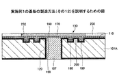
図1は、本発明の実施例1による基板を用いたパッケージ100を模式的に示す縦断面図である。図1を参照するに、パッケージ100は、例えばSiよりなる基板101に、光機能素子として、例えばLEDよりなる発光素子102が実装されてなる半導体装置である。発光素子102は、サファイア(Al2O3)を基材としてP層、N層、電極などが形成されている。
FIG. 1 is a longitudinal sectional view schematically showing a
尚、本実施例では、発光素子102が基板101に実装される構成について説明しているが、発光素子のみではなく、例えば、受光素子あるいはMEMS素子を実装した構成の半導体装置にも本発明を適用することができるのは、勿論である。
In this embodiment, the structure in which the
また、発光素子102上には光透過性の、例えばガラスよりなる平板状のカバー103が設置される。
Further, a light-transmitting
また、基板101には、発光素子102を実装するためのベース101Aと、ベース101A上に起立する壁部101Bとにより画成された収納部101Cが設けられている。この収納部101Cは、基板101の上面側が開口となる向きで形成されている。そして、パッケージ100は、収納部101Cの周囲を囲むように形成された壁部101Bの上端がカバー103と接合されることで発光素子102を封止する構成となる。すなわち、発光素子102は、気密に封止された密閉空間である収納部101Cに実装される。このため、収納部101Cを、例えば減圧状態としたり、または不活性ガスで満たすことが可能となり、発光素子102の性能の維持と長寿命化を図ることが可能となる。
The
また、基板101とカバー103とが陽極接合により接続されていると、例えば樹脂などの有機材料により接合される場合にくらべて発光素子102が封止される空間が清浄に保持されるため、発光素子102の品質が良好となり、好ましい。
In addition, when the
また、発光素子102は、例えばAuよりなるバンプ106上に設置され、当該バンプ106は例えばAu層が表面となるようにNi層とAu層が積層されてなる接続層106Aを介して基板101の底面を貫通するように形成される貫通電極107と電気的に接続されている。また、接続層106Aは、Ni/Pd/Auめっき層(Auが表面になる)あるいは他のめっき層を用いても良い。
The
貫通電極107の、発光素子102が接続される側の反対側(図1中、下端側)には、例えばAu層が表面となるようにNi層とAu層が積層されてなる接続層108Aが形成され、さらに当該接続層108Aに半田バンプ108が形成されている。すなわち、貫通電極107が形成されることによって、発光素子102と、当該発光素子102が封止される空間の外側の接続対象とを、容易に接続することが可能になっている。また、半田バンプ108と貫通電極107の間にも、例えばNi/Auメッキ層よりなる接続層が形成されていてもよいが、本図では図示を省略している。
On the opposite side of the through
また、基板101の下面には、絶縁層(シリコン酸化膜)110が形成され、例えば当該基板101と、貫通電極107との間や、バンプ106との間は絶縁層110によって絶縁されている。
In addition, an insulating layer (silicon oxide film) 110 is formed on the lower surface of the
ここで、基板101のベース101Aを貫通する貫通孔120及び貫通孔120に形成された貫通電極107の封止構造について説明する。図1において、拡大して示す部分が、基板101の封止構造130である。この封止構造130は、貫通孔120の内部の円筒状空間にCuまたはNiを電解めっき法などにより成長させてなる貫通電極107と貫通孔120の内壁に積層された絶縁層(シリコン酸化膜)110との間での密着性が劣化した場合に微小な隙間が生じ、この隙間によって収納部101Cに外気が侵入したり、あるいは収納部101Cに加圧された不活性ガスが外部に漏れたりすることを防止するための封止構造である。
Here, a sealing structure of the through-
封止構造130は、ベース101Aの下面側表面に形成された凹凸部140と、この凹凸部140の表面に積層された密着層150と、密着層150に積層された給電層160と、給電層160の表面に積層された電極層170とから構成されている。
The sealing
凹凸部140は、貫通電極107の外周または貫通孔120の内壁から半径方向に所定距離L1(例えば、10μm〜100μm)離間した位置に形成された第1凹部180と、第1凹部180よりさらに外側へ所定距離L2(例えば、10μm〜100μm)離間した位置に形成された第2凹部190とを有する。
The concavo-
また、第1凹部180と第2凹部190との間には、凸部200が形成されている。凸部200の半径方向の幅L3(例えば、10μm〜100μm)は、第1凹部180と第2凹部190との間隔(離間距離)に等しい。尚、本実施例では、各距離L1,L2,L3が等間隔となるように設定されているが、夫々異なる距離にして不均一な間隔で配置されるようにしても良い。
In addition, a
このように貫通電極107の外周または貫通孔120の内壁から半径方向の異なる位置に第1凹部180、凸部200、第2凹部190が形成されることで凹凸部140に対する密着層150の接合長さLは、電極層170の半径Rに半径方向及び垂直方向の段差部分の長さH(第1凹部180、第2凹部190の深さ)の4倍を加算した長さとなる(L=R+4H)。そのため、電極層170の半径Rよりも第1凹部180、第2凹部190の段差数分だけ接合距離が延長されたことになり、ベース101Aと電極層170との接合強度が高まると共に、ベース101Aの下面側表面での気密性が格段に高められている。
As described above, the first
この第1凹部180、第2凹部190の深さHは、電極層170の半径Rや貫通孔120の内径などに対応する所定値(例えば、1μm〜50μm)に設定される。第1凹部180、第2凹部190の深さHは、同一寸法でも良いし、夫々が異なる寸法となるようにしても良い。
The depth H of the
尚、第1凹部180、第2凹部190の半径方向の位置、及び深さは、上記括弧内の数値に限るものではなく、夫々貫通電極107の直径(貫通孔120の内径)や基板101またはベース101Aの厚さ等によって任意に選択される数値が設定される。
The positions and depths of the
ここで、上記パッケージ100に用いられる封止構造130を製造する製造方法の一例について、図2A〜図2Kに基づき、手順(その1〜11)を説明する。ただし、以下の図中、先に説明した部分には同一の参照符号を付し、説明を省略する場合がある。
Here, an example of a manufacturing method for manufacturing the sealing
まず、図2Aに示す工程において、例えばSiよりなる基板101の上面側をエッチングしてパターニングし、発光素子102(図1参照)を設置するための収納部101Cを形成する。尚、本実施例では、基板101の上面側からエッチングして発光素子102を収納する収納部101Cを形成する製造方法について説明するが、基板101の厚さが薄い場合には、平板状に形成された基板の表面に発光素子102の周囲を囲むための壁を積層して収納部を形成する製造方法を用いて良い。
First, in the step shown in FIG. 2A, for example, the upper surface side of the
次に、図2Bに示す工程において、貫通電極107を形成するための貫通孔120を、エッチングにより基板101のベース101Aを上下方向に貫通するように形成する。
この後の工程では、図2B中に示す貫通孔120及びその周辺を囲むA部に封止構造130を形成する際の手順について説明する。
Next, in the step shown in FIG. 2B, a through
In the subsequent steps, a procedure for forming the sealing
次に、図2Cに示す工程において、ベース101Aの下面側(図2Cでは説明の便宜上下方向を逆向きに示す)の表面101Dにドライフィルムレジスト等のレジスト210を積層する。
Next, in the step shown in FIG. 2C, a resist 210 such as a dry film resist is laminated on the
次に、図2Dに示す工程において、レジスト210をパターニング(露光、現像)して前述した第1凹部180、第2凹部190の形成位置に対応する箇所から除去する。パターニングによりレジスト210に形成された開口212、214は、第1凹部180、第2凹部190の輪郭形状に対応しており、夫々貫通孔120から半径方向に所定距離離間した位置で貫通孔120を囲むように同心円状、または貫通孔120を中心とする四角形状の枠状に形成される。
Next, in the step shown in FIG. 2D, the resist 210 is patterned (exposed and developed) and removed from the locations corresponding to the positions where the
次に、図2Eに示す工程において、パターニングされたレジスト210の開口212、214内に露出するベース101Aの表面101Dにエッチング処理を施し、第1凹部180、第2凹部190からなる環状溝(上方からみて環状)または四角枠状溝(上方からみて四角形)を形成する。実際は、ベース101Aの上面側の面がレジスト210等によりマスクされた状態でエッチングが行なわれるため、ベース101Aの表面101Dに開口212、214のパターン形状(上方からみた形状)に応じた形状の第1凹部180、第2凹部190がエッチングされる。従って、レジスト210の開口212、214の各寸法や間隔を換えることにより、第1凹部180、第2凹部190を任意の寸法及び間隔に形成することが可能になる。
Next, in the step shown in FIG. 2E, the
次に、図2Fに示す工程において、剥離液により膨潤、軟化させ、ブラッシングによりレジスト210を除去する。これにより、ベース101Aの表面101Dに、貫通孔120の周囲を囲むように第1凹部180、第2凹部190、凸部200が同心円状または四角枠状に形成された状態の基板101が得られる。
Next, in the step shown in FIG. 2F, the resist 210 is swollen and softened by a stripping solution and the resist 210 is removed by brushing. Thereby, the
次に、図2Gに示す工程において、ベース101Aの下面(第1凹部180、第2凹部190、凸部200の表面を含む)、収納部101Cの内壁面や貫通孔120の内壁面を含む基板101の表面に、例えば熱CVD法などにより、酸化膜(シリコン酸化膜、または熱酸化膜と呼ぶ場合もある)からなる絶縁層110を形成する。
Next, in the step shown in FIG. 2G, the substrate including the lower surface of the
次に、図2Hに示す工程において、例えば基板101のベース101Aの下面側に導電性テープ220(図2H中、一点鎖線で示す)を貼り付ける。そして、この導電性テープ220を給電層として電解めっき法等により貫通孔120にCu層またはNi層を成長させる。これにより、貫通孔120には、CuまたはNiが析出して得られた貫通電極107が形成される。そして、貫通孔120に貫通電極107が形成された後は、導電性テープ220をベース101Aの下面から剥がして除去する。
Next, in the step shown in FIG. 2H, for example, a conductive tape 220 (indicated by a one-dot chain line in FIG. 2H) is attached to the lower surface side of the
次に、図2Iに示す工程において、PVD(Physical Vapor Deposition)法またはCVD(Chemical Vapor Deposition)法により絶縁層110に対して良好な密着性を有する密着メタル(例えば、Ti,Ta,Crなど)を第1凹部180、第2凹部190、凸部200、貫通電極107を含むベース101Aの表面101D全体に蒸着させて密着層150を積層する。
Next, in the step shown in FIG. 2I, an adhesion metal (eg, Ti, Ta, Cr, etc.) having good adhesion to the insulating
そのため、密着層150の表面は、貫通孔120の内壁(または貫通電極107の外周)からの周縁部までの半径方向(周辺方向)の長さに、第1凹部180、第2凹部190、凸部200の上下方向の深さ(または高さ)を加算した距離を有する。このように密着層150は、第1凹部180、第2凹部190、凸部200の表面(半径方向及び上下方向の壁面を含む)に接合されるため、絶縁層110との間の気密性が高められており、絶縁層110に対して強固に積層される。
For this reason, the surface of the
次に、図2Jに示す工程において、PVD法または無電解めっき法により一例としてCu等からなる給電層160を密着層150の表面に積層する。給電層160は、密着性の高い密着層150に接合されると共に、第1凹部180、第2凹部190、凸部200の表面(上下方向の壁面を含む)にも接合されるため、平坦面に接合する場合よりも接合距離が大幅に延長されることにより、密着層150と給電層160との間の気密性が高められており、密着層150に対して強固に積層される。
Next, in the step shown in FIG. 2J, as an example, a
次に、図2Kに示す工程において、給電層160の表面にめっきレジスト230を形成し、次いでめっきレジスト230をパターニング(露光、現像)して前述した電極層170の形成位置に対応する箇所を除去して電極層形成用開口232を形成する。電極層形成用開口232は、第1凹部180、第2凹部190、凸部200が露出するように上方からみて貫通電極107の軸心を中心とする円形または四角形状に形成される。
Next, in the step shown in FIG. 2K, a plating resist 230 is formed on the surface of the
次に、図2Lに示す工程において、セミアディティブ法により給電層160からの給電による電解めっきを施して給電層160の表面にCuめっき層からなる電極層170を積層する。また、電極層170はサブトラクティブ法などセミアディティブ法以外の方法で形成するようにしても良い。
Next, in the step shown in FIG. 2L, an
このように、電極層170は、第1凹部180、第2凹部190、凸部200の表面に絶縁層110、密着層150、給電層160を介して接合されるため、平坦面に接合する場合よりも接合距離が大幅に延長されることにより、給電層160との間の気密性が高められており、給電層160に対して強固に積層される。
As described above, since the
次に、図2Mに示す工程において、レジスト230を除去し、次いで電極層170の下方部分を除く領域(電極層170の外側の領域)の密着層150と給電層160をエッチングにより除去する。これで、図1に示す封止構造130が完成する。
Next, in the step shown in FIG. 2M, the resist 230 is removed, and then the
このように、封止構造130は、ベース101Aの表面に形成された第1凹部180、第2凹部190、凸部200の表面(上下方向の壁面を含む)に絶縁層110、密着層150、給電層160、電極層170を積層する構成であるので、貫通孔120の内壁と貫通電極107の外周との間に微細な隙間が発生した場合でも、貫通電極107の周囲の気密性を高めることができると共に、平坦面のものよりも接合強度をより一層高めることが可能になる。
As described above, the sealing
続いて、上記封止構造130を有する基板101の収納部101Cに発光素子102を実装する手順(その1〜9)について図3A〜図3Iに基づいて説明する。ただし、以下の図中、先に説明した部分には同一の参照符号を付し、説明を省略する場合がある。
Next, a procedure (Nos. 1 to 9) for mounting the
まず、図3Aに示す工程において、ベース101Aの下面側には、複数の収納部101Cの夫々に設けられた貫通電極107の周辺に気密性が確保された封止構造130が形成されている。
First, in the step shown in FIG. 3A, a sealing
次に、図3Bに示す工程において、例えばメッキ法により、例えばNi/Auよりなる接続層106A,108Aを形成する。この場合、接続層106Aは、それぞれ貫通電極107の上端側(収納部101C側)に形成される。また、接続層108Aは、それぞれ貫通電極107の反対側(下端側)の電極層170上に形成される。
Next, in the step shown in FIG. 3B, connection layers 106A and 108A made of, for example, Ni / Au are formed by, for example, plating. In this case, the
次に、図3Cに示す工程において、接続層106A上に、一例としてAuワイヤのワイヤボンディングにより、それぞれバンプ106を形成する。なお、本図以降では、接続層106Aの図示を省略している。
Next, in the step shown in FIG. 3C, bumps 106 are formed on the
次に、図3Dに示す工程において、収納部101Cの周囲の壁部101Bの上端側表面に形成された絶縁層110を、例えばマスクエッチにより剥離する。本工程によって絶縁層110が除去された壁部101Bの上端には、後の工程においてガラスよりなるカバーを接合することが可能になる。
Next, in the step shown in FIG. 3D, the insulating
次に、図3Eに示す工程において、発光素子102を収納部101C内に設置する。この場合、例えば熱圧着、または超音波接合などを用いて、発光素子102の電極とバンプ106を電気的に接合し、バンプ106を介して発光素子102と貫通電極107が電気的に接続されるように構成する。
Next, in the step shown in FIG. 3E, the
次に、図3Fに示す工程において、例えばホウケイ酸ガラスよりなる、透過性を有する平板状のカバー103と基板101の壁部101Bの上端面を、例えば陽極接合法により接合し、発光素子102を基板101の収納部101C内に封止する構造が形成される。この場合、陽極接合法では、カバー103と基板101との間に高電圧を印加し、カバー103と基板101を昇温することでカバー103と壁部101Bの上端面とを接合する。
Next, in the step shown in FIG. 3F, the flat plate-
上記の陽極接合が行われると、基板を構成するSiと、カバーを構成するガラス中の酸素が結合し、接合力が良好で安定した接合が行われる。また、樹脂材料を用いた接合と異なり、発光素子102が封止される空間を汚染するようなガス、不純物などが殆ど発生することがない。
When the above-described anodic bonding is performed, Si constituting the substrate and oxygen in the glass constituting the cover are bonded to each other, and the bonding force is good and stable bonding is performed. Unlike bonding using a resin material, almost no gas, impurities, or the like that contaminates the space in which the light-emitting
次に、図3Gに示す工程において、接続層108Aに半田バンプ108を形成する。
Next, in the step shown in FIG. 3G, solder bumps 108 are formed on the
次に、図3Hに示す工程において、基板101とカバー103をダイシングにより切断し、個片化することで、先に説明したパッケージ100(図1を参照)が完成する。
Next, in the step shown in FIG. 3H, the
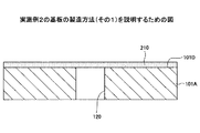
図4は実施例2による基板に用いられた封止構造を模式的に示す縦断面図である。パッケージ100に用いられる封止構造の実施例2について、図4に基づき説明する。以下の図中、先に説明した部分には同一の参照符号を付し、説明を省略する場合がある。
FIG. 4 is a longitudinal sectional view schematically showing the sealing structure used for the substrate according to the second embodiment. Example 2 of the sealing structure used for the
図4に示されるように、実施例2の封止構造330は、ベース101Aの下面側表面に形成された凹凸部340と、この凹凸部340の表面に積層された密着層150と、密着層150に積層された給電層160と、給電層160の表面に積層された電極層170とから構成されている。
As shown in FIG. 4, the sealing
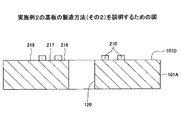
凹凸部340は、貫通電極107の外周または貫通孔120の内壁に対して半径方向に所定距離L1(例えば、10μm〜100μm)離間した位置に形成された第1凸部380と、第1凸部380よりさらに外側へ所定距離L2(例えば、10μm〜100μm)離間した位置に形成された第2凸部390とを有する。
The concavo-
また、第1凸部380と第2凸部390との間には、凹部400が形成されている。凹部400の半径方向の幅L3(例えば、10μm〜100μm)は、第1凸部380と第2凸部390との間隔(離間距離)に等しい。尚、本実施例では、各距離L1,L2,L3が等間隔となるように設定されているが、夫々異なる距離にして不均一な間隔で配置されるようにしても良い。
In addition, a
このように貫通電極107の外周または貫通孔120の内壁から半径方向の異なる位置に第1凸部380、凹部400、第2凸部390が形成されることで凹凸部340に対する密着層150の接合長さLは、電極層170の半径Rに半径方向及び垂直方向の段差部分の長さH(第1凸部380、第2凸部390の高さ)の4倍を加算した長さとなる(L=R+4H)。そのため、電極層170の半径Rよりも第1凸部380、第2凸部390の段差数分だけ接合距離が延長されたことになり、ベース101Aと電極層170との接合強度が高まると共に、ベース101Aの下面側表面での気密性が格段に高められている。
As described above, the first
この第1凸部380、第2凸部390の高さHは、電極層170の半径Rや貫通孔120の内径などに対応する所定値(例えば、1μm〜10μm)に設定される。第1凸部380、第2凸部390の高さHは、同一寸法でも良いし、夫々が異なる寸法となるようにしても良い。
The height H of the
尚、第1凸部380、第2凸部390の半径方向の位置、及び高さは、上記括弧内の数値に限るものではなく、夫々貫通電極107の直径(貫通孔120の内径)や基板101またはベース101Aの厚さ等によって任意に選択される数値が設定される。
Note that the radial positions and heights of the first
次に、上記の封止構造330を製造する製造方法について、図5A〜図5Iに基づき、手順(その1〜9)を説明する。尚、図5A〜図5Iに示す各工程は、前述した図2C〜図2Kに示す工程の別の実施例に相当する。以下の図中、先に説明した部分には同一の参照符号を付し、説明を省略する場合がある。
Next, about the manufacturing method which manufactures said sealing
まず、図5Aに示す工程において、ベース101Aの下面側(図5Aでは説明の便宜上下方向を逆向きに示す)の表面101Dにドライフィルムレジスト等のレジスト210を積層する。
First, in the step shown in FIG. 5A, a resist 210 such as a dry film resist is laminated on the
次に、図5Bに示す工程において、レジスト210をパターニング(露光、現像)して前述した第1凸部380、第2凸部390の形成位置に対応する箇所を除く部分から除去して第1凸部380、第2凸部390の形成位置に対応する箇所にレジスト210を残す。ベース101Aの表面101Dに残されたレジスト210のパターンは、第1凸部380、第2凸部390の輪郭形状に対応しており、夫々貫通孔120から半径方向に所定距離離間した位置で貫通孔120を囲むように同心円状、または貫通孔120を中心とする四角形状の枠状に形成される。
Next, in the step shown in FIG. 5B, the resist 210 is patterned (exposure and development) and removed from portions other than the portions corresponding to the formation positions of the first
次に、図5Cに示す工程において、パターニングされたレジスト210の間に形成された開口216,217,218内に露出するベース101Aの表面101Dにエッチング処理を施す。これにより、レジスト210が積層されていない部分の表面101Dが除去されるため、相対的に第1凸部380、第2凸部390からなる環状凸部(上方からみて環状)または四角枠状凸部(上方からみて四角形)、及び凹部400が形成される。
Next, in the step shown in FIG. 5C, the
実際は、ベース101Aの上面側の面がレジスト210等によりマスクされた状態でエッチングが行なわれるため、開口216,217,218のパターン形状(上方からみた形状)に応じた貫通孔120の周囲及びその外側に位置する凹部400がエッチングされる。従って、レジスト210の開口216,217,218の各寸法や間隔を換えることにより、第1凸部380、第2凸部390を任意の寸法及び間隔に形成することが可能になる。
Actually, the etching is performed in a state where the upper surface of the
次に、図5Dに示す工程において、剥離液により膨潤、軟化させ、ブラッシングによりレジスト210を除去する。これにより、ベース101Aの表面101Dに、貫通孔120の周囲を囲むように第1凸部380、第2凸部390、凹部400が上方からみて同心円状または四角枠状に形成された状態の基板101が得られる。
Next, in the step shown in FIG. 5D, the resist 210 is swollen and softened with a stripping solution, and the resist 210 is removed by brushing. As a result, the first
次に、図5Eに示す工程において、ベース101Aの下面(第1凸部380、第2凸部390、凹部400の表面を含む)、収納部101Cの内壁面や貫通孔120の内壁面を含む基板101の表面に、例えば熱CVD法などにより、酸化膜(シリコン酸化膜、または熱酸化膜と呼ぶ場合もある)からなる絶縁層110を形成する。
Next, in the step shown in FIG. 5E, the lower surface of the
次に、図5Fに示す工程において、例えば基板101のベース101Aの下面側に導電性テープ220(図5F中、一点鎖線で示す)を貼り付ける。そして、この導電性テープ220を給電層として電解めっき法等により貫通孔120にCu層またはNi層を成長させる。これにより、貫通孔120には、CuまたはNiが析出して得られた貫通電極107が形成される。そして、貫通孔120に貫通電極107が形成された後は、導電性テープ220をベース101Aの下面から剥がして除去する。
Next, in the step illustrated in FIG. 5F, for example, a conductive tape 220 (indicated by a one-dot chain line in FIG. 5F) is attached to the lower surface side of the
次に、図5Gに示す工程において、PVD(Physical Vapor Deposition)法またはCVD(Chemical Vapor Deposition)法により絶縁層110に対して良好な密着性を有する密着メタル(例えば、Ti,Ta,Crなど)を第1凸部380、第2凸部390、凹部400貫通電極107を含むベース101Aの表面全体に蒸着させて密着層150を積層する。
そのため、密着層150の表面は、貫通孔120の内壁(または貫通電極107の外周)からの周縁部までの半径方向(周辺方向)の長さに、第1凸部380、第2凸部390、凹部400の上下方向の深さ(または高さ)を加算した距離を有する。このように密着層150は、第1凸部380、第2凸部390、凹部400の表面(半径方向及び上下方向の壁面を含む)に接合されるため、絶縁層110との間の気密性が高められており、絶縁層110に対して強固に積層される。
Next, in the step shown in FIG. 5G, an adhesion metal (eg, Ti, Ta, Cr, etc.) having good adhesion to the insulating
Therefore, the surface of the
次に、図5Hに示す工程において、PVD法または無電解めっき法により一例としてCu等からなる給電層160を密着層150の表面に積層する。給電層160は、密着性の高い密着層150に接合されると共に、第1凸部380、第2凸部390、凹部400の表面(上下方向の壁面を含む)にも接合されるため、平坦面に接合する場合よりも接合距離が大幅に延長されることにより、密着層150と給電層160との間の気密性が高められており、密着層150に対して強固に積層される。
Next, in the step shown in FIG. 5H, a
次に、図5Iに示す工程において、給電層160の表面にめっきレジスト230を形成し、次いでめっきレジスト230をパターニング(露光、現像)して前述した電極層170の形成位置に対応する箇所を除去して電極層形成用開口232を形成する。電極層形成用開口232は、第1凹部180、第2凹部190、凸部200が露出するように上方からみて貫通電極107の軸心を中心とする円形または四角形状に形成される。
Next, in the step shown in FIG. 5I, a plating resist 230 is formed on the surface of the
次に、図5Jに示す工程において、セミアディティブ法により給電層160からの給電による電解めっきを施して給電層160の表面にCuめっき層からなる電極層170を積層する。また、電極層170はサブトラクティブ法などセミアディティブ法以外の方法で形成するようにしても良い。このように、電極層170は、第1凸部380、第2凸部390、凹部400の表面に絶縁層110、密着層150、給電層160を介して接合されるため、平坦面に接合する場合よりも接合距離が大幅に延長されることにより、給電層160との間の気密性が高められており、給電層160に対して強固に積層される。
Next, in the step shown in FIG. 5J, the
次に、図5Kに示す工程において、レジスト230を除去し、次いで電極層170の下方部分を除く領域(電極層170の外側の領域)の密着層150と給電層160をエッチングにより除去する。これで、図4に示す封止構造330が完成する。
Next, in the step shown in FIG. 5K, the resist 230 is removed, and then the
このように、封止構造330は、ベース101Aの表面に形成された第1凸部380、第2凸部390、凹部400の表面(上下方向の壁面を含む)に絶縁層110、密着層150、給電層160、電極層170を積層する構成であるので、貫通孔120の内壁と貫通電極107の外周との間に微細な隙間が発生した場合でも、貫通電極107の周囲の気密性を高めることができると共に、平坦面のものよりも接合強度をより一層高めることが可能になる。
As described above, the sealing
図6は実施例3による基板に用いられた封止構造を模式的に示す縦断面図である。パッケージ100に用いられる封止構造の実施例3について、図6に基づき説明する。以下の図中、先に説明した部分には同一の参照符号を付し、説明を省略する場合がある。
6 is a longitudinal sectional view schematically showing a sealing structure used for a substrate according to Example 3. FIG. Example 3 of the sealing structure used for the
図6に示されるように、実施例3の封止構造430は、貫通孔120の開口の内壁に微小な凹凸による粗面440が形成されている。この粗面440は、前述した実施例1の図2Bの工程において、エッチングにより基板101のベース101Aを上下方向に貫通する貫通孔120を形成した後、貫通孔120の内壁全面または貫通孔120の一部(開口端側)の内壁にハーフエッチングによる粗化処理を施すことにより形成される。
As shown in FIG. 6, the sealing
その後、前述した実施例1の図2G、図2I、図2J、図2Lの工程により、ベース101Aの全面及び貫通孔120の内壁(粗面440を含む)に絶縁層110、密着層150、給電層160を積層し、レジスト230の電極層形成用開口232に電極層170を形成する。また、図2Hの工程により貫通電極107を形成する際は、電解めっき時間を短縮することにより、貫通孔120の開口の一端側の内壁が露出するように貫通電極107の一端が貫通孔120の開口端より低くなるように貫通電極107を形成する。
2G, FIG. 2I, FIG. 2J, and FIG. 2L of the first embodiment described above, the insulating
さらに、密着層150は、粗面440の表面に均一な膜厚で積層されることが望ましい。この密着層150は、例えば、分子レベルでの均一な薄膜形成が可能なALD(アトミック・レイア・デポジジョン)で行なうことが好ましい。そして、微小な凹凸を有する密着層150の表面には、均一な膜厚を有する給電層160が積層されることが望ましい。
Furthermore, it is desirable that the
さらに、セミアディティブ法により給電層160からの給電による電解めっきを施して給電層160の表面にCuめっき層からなる電極層170を積層する。また、電極層170はサブトラクティブ法などセミアディティブ法以外の方法で形成するようにしても良い。
Further, the
これにより、電極層170は、実施例1,2と同様に、実施例1の第1凹部180、第2凹部190(あるいは実施例2の第1凸部380、第2凸部390)の表面に積層されると共に、貫通孔120の開口の一端側の内壁に形成された微小な凹凸を有する粗面440の表面に絶縁層110、密着層150、給電層160を介して接合される。そのため、電極層170は、給電層160との間の気密性がより高められており、給電層160に対して強固に積層される。
Thereby, the
また、実施例3では、貫通孔120の内壁に粗面440と、実施例1の第1凹部180、第2凹部190あるいは実施例2の第1凸部380、第2凸部390とを組み合わせてなるため、上記実施例1,2よりも密着層150、給電層160、電極層170との間の気密性がより一層高められており、給電層160に対して強固に積層される。
In the third embodiment, the inner wall of the through-
上記実施例では、基板101の収納部101Cに発光素子102が実装された場合を例に挙げて説明したが、これに限らず、発光素子102以外の素子(例えば、MEMS素子など)が実装される基板の封止構造にも本発明が適用できるのは勿論である。
また、上記各実施例では、基板101の下面側のみに第1凹部180、第2凹部190あるいは第1凸部380、第2凸部390を設ける構成について説明したが、これに限らず、基板101の上面側及び下面側(貫通電極107の両端側)に第1凹部180、第2凹部190あるいは第1凸部380、第2凸部390を設けるようにしても良いのは勿論である。また、上記実施例3の粗面400を貫通電極107の両端側の開口内壁に形成し、絶縁層110、密着層150、給電層160を介して電極層170を積層するようにしても良い。
In the above embodiment, the case where the
In each of the above embodiments, the configuration in which the first
また、上記各実施例では、発光素子102が実装される基板101に貫通電極107を設ける構成を一例として説明したが、これに限らず、例えば、集積回路が形成されたシリコン基板に貫通電極107を設けると共に、上記実施例1の封止構造130、または実施例2の封止構造530、または貫通孔120の開口内壁に粗面440を形成し、粗面440に絶縁層110、密着層150、給電層160を介して電極層170を積層する構成を適用することも可能である。
In each of the above-described embodiments, the configuration in which the through
100 パッケージ
101 基板
101A ベース
101B 壁部
101C 収納部
102 発光素子
103 カバー
107 貫通電極
108 半田バンプ
110 絶縁層
120 貫通孔
130,330,430 封止構造
140 凹凸部
150 密着層
160 給電層
170 電極層
180 第1凹部
190 第2凹部
200 凸部
380 第1凸部
390 第2凸部
400 凹部
440 粗面
DESCRIPTION OF
Claims (23)
前記貫通電極の端部周辺に位置する前記基板表面に少なくとも凹部または凸部の何れか一方を含む凹凸部を形成する工程と、
前記貫通電極の端部表面及び前記凹凸部の表面に外部接続用の電極層を形成する工程と、
を有することを特徴とする基板の製造方法。 In a method for manufacturing a substrate having a through electrode,
Forming a concavo-convex portion including at least one of a concave portion and a convex portion on the substrate surface located around the end portion of the through electrode; and
Forming an electrode layer for external connection on the end surface of the through electrode and the surface of the uneven portion;
A method for manufacturing a substrate, comprising:
前記凹凸部の表面に前記絶縁層に対する密着性及び導電性を有する密着層を形成する工程と、をさらに有することを特徴とする請求項1乃至4の何れかに記載の基板の製造方法。 The method for manufacturing a substrate according to claim 1, further comprising: forming an adhesion layer having adhesion and conductivity to the insulating layer on a surface of the uneven portion.
前記貫通孔内の途中まで前記貫通電極を形成する工程と、をさらに有することを特徴とする請求項1乃至10の何れかに記載の基板の製造方法。 Forming a through hole for forming the pre SL through electrodes,
A method for manufacturing a substrate according to any one of claims 1 to 10, characterized that you have further, the step of forming the through-electrode to the middle of the through hole.
基板表面の前記貫通電極の端部周辺に形成され、少なくとも凹部または凸部の何れか一方を含む凹凸部と、
前記貫通電極の端部表面及び前記凹凸部の表面に形成される外部接続用の電極層と
を備えたことを特徴とする基板。 In a substrate having a through electrode,
An uneven portion that is formed around the end portion of the through electrode on the surface of the substrate and includes at least one of a concave portion or a convex portion,
A substrate comprising: an electrode layer for external connection formed on an end surface of the through electrode and a surface of the uneven portion.
前記凹凸部の表面に積層され、前記絶縁層に対する密着性及び導電性を有する密着層を有することを特徴とする請求項13乃至17の何れかに記載の基板。 The substrate according to any one of claims 13 to 17, further comprising an adhesion layer that is laminated on a surface of the uneven portion and has adhesion and conductivity to the insulating layer.
Priority Applications (5)
| Application Number | Priority Date | Filing Date | Title |
|---|---|---|---|
| JP2007097614A JP5154819B2 (en) | 2007-04-03 | 2007-04-03 | Substrate and manufacturing method thereof |
| KR1020080030590A KR20080090307A (en) | 2007-04-03 | 2008-04-02 | Substrate and method for manufacturing the same |
| US12/061,203 US8481863B2 (en) | 2007-04-03 | 2008-04-02 | Substrate and method for manufacturing the same |
| EP08154036.1A EP1978558B1 (en) | 2007-04-03 | 2008-04-03 | Substrate and method for manufacturing the same |
| TW097112124A TW200847366A (en) | 2007-04-03 | 2008-04-03 | Substrate and method for manufacturing the same |
Applications Claiming Priority (1)
| Application Number | Priority Date | Filing Date | Title |
|---|---|---|---|
| JP2007097614A JP5154819B2 (en) | 2007-04-03 | 2007-04-03 | Substrate and manufacturing method thereof |
Publications (2)
| Publication Number | Publication Date |
|---|---|
| JP2008258322A JP2008258322A (en) | 2008-10-23 |
| JP5154819B2 true JP5154819B2 (en) | 2013-02-27 |
Family
ID=39430083
Family Applications (1)
| Application Number | Title | Priority Date | Filing Date |
|---|---|---|---|
| JP2007097614A Active JP5154819B2 (en) | 2007-04-03 | 2007-04-03 | Substrate and manufacturing method thereof |
Country Status (5)
| Country | Link |
|---|---|
| US (1) | US8481863B2 (en) |
| EP (1) | EP1978558B1 (en) |
| JP (1) | JP5154819B2 (en) |
| KR (1) | KR20080090307A (en) |
| TW (1) | TW200847366A (en) |
Families Citing this family (14)
| Publication number | Priority date | Publication date | Assignee | Title |
|---|---|---|---|---|
| TWI453878B (en) * | 2009-01-10 | 2014-09-21 | Unimicron Technology Corp | Package substrate and method for fabricating same |
| JP5139347B2 (en) * | 2009-02-18 | 2013-02-06 | 新光電気工業株式会社 | Electronic component device and manufacturing method thereof |
| KR101091304B1 (en) | 2010-01-20 | 2011-12-07 | 엘지이노텍 주식회사 | Light emitting device package and fabricating method thereof |
| KR101637581B1 (en) * | 2010-03-09 | 2016-07-07 | 엘지이노텍 주식회사 | Light emitting device package and fabricating method thereof |
| CN102244178A (en) * | 2010-05-14 | 2011-11-16 | 展晶科技(深圳)有限公司 | Encapsulation structure of LED (light emitting diode) |
| CN102270725A (en) * | 2010-06-01 | 2011-12-07 | 展晶科技(深圳)有限公司 | Light emitting diode packaging structure |
| CN102315354B (en) * | 2010-06-29 | 2013-11-06 | 展晶科技(深圳)有限公司 | Packaging structure of light emitting diode |
| US9704793B2 (en) | 2011-01-04 | 2017-07-11 | Napra Co., Ltd. | Substrate for electronic device and electronic device |
| KR102059402B1 (en) * | 2013-04-15 | 2019-12-26 | 삼성전자주식회사 | Electronic device package and packaging substrate for the same |
| JP6185415B2 (en) | 2014-03-27 | 2017-08-23 | 株式会社東芝 | Semiconductor light emitting device |
| KR20170011366A (en) * | 2015-07-22 | 2017-02-02 | 삼성전자주식회사 | Semiconductor chip and semiconductor package having the same |
| US11282717B2 (en) * | 2018-03-30 | 2022-03-22 | Intel Corporation | Micro-electronic package with substrate protrusion to facilitate dispense of underfill between a narrow die-to-die gap |
| CN110400860A (en) * | 2019-07-23 | 2019-11-01 | 华引芯(武汉)科技有限公司 | A kind of UV LED full-inorganic sealing structure and preparation method thereof |
| JP7469348B2 (en) | 2022-03-16 | 2024-04-16 | アオイ電子株式会社 | Wiring board and method for manufacturing the same |
Family Cites Families (16)
| Publication number | Priority date | Publication date | Assignee | Title |
|---|---|---|---|---|
| JPS62216259A (en) * | 1986-03-17 | 1987-09-22 | Fujitsu Ltd | Manufacture and structure of hybrid integrated circuit |
| JPH02324A (en) * | 1987-12-18 | 1990-01-05 | Mitsui Mining & Smelting Co Ltd | Conducting film circuit and its manufacture |
| JP3317193B2 (en) * | 1997-06-30 | 2002-08-26 | 株式会社村田製作所 | Electronic component package structure and method of manufacturing the same |
| JP4480207B2 (en) * | 1999-01-04 | 2010-06-16 | イビデン株式会社 | Resin package substrate |
| EP1211920B1 (en) * | 1999-08-12 | 2010-09-15 | Ibiden Co., Ltd. | Multilayer printed wiring board and method for manufacturing multilayer printed wiring board |
| JP2002118338A (en) * | 2000-10-06 | 2002-04-19 | Matsushita Electric Ind Co Ltd | Circuit board and its manufacturing method |
| JP2004228392A (en) | 2003-01-24 | 2004-08-12 | Seiko Epson Corp | Manufacturing method of semiconductor device and manufacturing method of semiconductor module |
| JP2004327910A (en) | 2003-04-28 | 2004-11-18 | Sharp Corp | Semiconductor device and its manufacturing method |
| JP2005019966A (en) * | 2003-06-06 | 2005-01-20 | Sanyo Electric Co Ltd | Semiconductor device and method of manufacturing the same |
| JP4098673B2 (en) * | 2003-06-19 | 2008-06-11 | 新光電気工業株式会社 | Manufacturing method of semiconductor package |
| JP3751625B2 (en) * | 2004-06-29 | 2006-03-01 | 新光電気工業株式会社 | Manufacturing method of through electrode |
| JP4873517B2 (en) | 2004-10-28 | 2012-02-08 | オンセミコンダクター・トレーディング・リミテッド | Semiconductor device and manufacturing method thereof |
| JP2007027279A (en) * | 2005-07-13 | 2007-02-01 | Shinko Electric Ind Co Ltd | Semiconductor device and manufacturing method thereof |
| JP2007067216A (en) | 2005-08-31 | 2007-03-15 | Sanyo Electric Co Ltd | Semiconductor device and manufacturing method thereof, and circuit board and manufacturing method thereof |
| JP4782526B2 (en) | 2005-09-30 | 2011-09-28 | Juki株式会社 | sewing machine |
| US7354799B2 (en) * | 2005-11-08 | 2008-04-08 | Intel Corporation | Methods for anchoring a seal ring to a substrate using vias and assemblies including an anchored seal ring |
-
2007
- 2007-04-03 JP JP2007097614A patent/JP5154819B2/en active Active
-
2008
- 2008-04-02 KR KR1020080030590A patent/KR20080090307A/en not_active Application Discontinuation
- 2008-04-02 US US12/061,203 patent/US8481863B2/en active Active
- 2008-04-03 EP EP08154036.1A patent/EP1978558B1/en active Active
- 2008-04-03 TW TW097112124A patent/TW200847366A/en unknown
Also Published As
| Publication number | Publication date |
|---|---|
| JP2008258322A (en) | 2008-10-23 |
| EP1978558A1 (en) | 2008-10-08 |
| KR20080090307A (en) | 2008-10-08 |
| TW200847366A (en) | 2008-12-01 |
| US20080251287A1 (en) | 2008-10-16 |
| EP1978558B1 (en) | 2017-09-13 |
| US8481863B2 (en) | 2013-07-09 |
Similar Documents
| Publication | Publication Date | Title |
|---|---|---|
| JP5154819B2 (en) | Substrate and manufacturing method thereof | |
| JP4828248B2 (en) | Light emitting device and manufacturing method thereof | |
| KR101591991B1 (en) | Light emitting device package and method thereof | |
| US7834438B2 (en) | Sealed structure and method of fabricating sealed structure and semiconductor device and method of fabricating semiconductor device | |
| JP5026038B2 (en) | Electronic component equipment | |
| JP5643880B2 (en) | MEMS device and manufacturing method thereof | |
| JP5137059B2 (en) | Electronic component package, manufacturing method thereof, and electronic component device | |
| JP5568786B2 (en) | Semiconductor package manufacturing method and semiconductor package | |
| CN102592982B (en) | Method for forming chip package | |
| JP2015133520A (en) | Chip package and fabrication method thereof | |
| US9136241B2 (en) | Chip package and manufacturing method thereof | |
| US8309388B2 (en) | MEMS package having formed metal lid | |
| US7829993B2 (en) | Semiconductor apparatus | |
| JP2007027279A (en) | Semiconductor device and manufacturing method thereof | |
| JP4539155B2 (en) | Manufacturing method of sensor system | |
| US20090242923A1 (en) | Hermetically Sealed Device with Transparent Window and Method of Manufacturing Same | |
| JP2009238957A (en) | Via forming method on board | |
| JP2007201361A (en) | Semiconductor device, and method of manufacturing semiconductor device | |
| TWI580081B (en) | Optoelectronic semiconductor component and method for producing the same | |
| JP5248179B2 (en) | Manufacturing method of electronic device | |
| JP2006186357A (en) | Sensor device and its manufacturing method | |
| JP2006201158A (en) | Sensor | |
| JP2013171930A (en) | Electronic component package and method for manufacturing the same | |
| JP2009206215A (en) | Manufacturing method of light emitting device | |
| JP2013173193A (en) | Mems module and method of manufacturing the same |
Legal Events
| Date | Code | Title | Description |
|---|---|---|---|
| A621 | Written request for application examination |
Free format text: JAPANESE INTERMEDIATE CODE: A621 Effective date: 20100119 |
|
| A977 | Report on retrieval |
Free format text: JAPANESE INTERMEDIATE CODE: A971007 Effective date: 20100528 |
|
| A131 | Notification of reasons for refusal |
Free format text: JAPANESE INTERMEDIATE CODE: A131 Effective date: 20120605 |
|
| A521 | Written amendment |
Free format text: JAPANESE INTERMEDIATE CODE: A523 Effective date: 20120802 |
|
| TRDD | Decision of grant or rejection written | ||
| A01 | Written decision to grant a patent or to grant a registration (utility model) |
Free format text: JAPANESE INTERMEDIATE CODE: A01 Effective date: 20121127 |
|
| A61 | First payment of annual fees (during grant procedure) |
Free format text: JAPANESE INTERMEDIATE CODE: A61 Effective date: 20121206 |
|
| FPAY | Renewal fee payment (event date is renewal date of database) |
Free format text: PAYMENT UNTIL: 20151214 Year of fee payment: 3 |
|
| R150 | Certificate of patent or registration of utility model |
Ref document number: 5154819 Country of ref document: JP Free format text: JAPANESE INTERMEDIATE CODE: R150 Free format text: JAPANESE INTERMEDIATE CODE: R150 |