EP1978558A1 - Substrate and method for manufacturing the same - Google Patents
Substrate and method for manufacturing the same Download PDFInfo
- Publication number
- EP1978558A1 EP1978558A1 EP08154036A EP08154036A EP1978558A1 EP 1978558 A1 EP1978558 A1 EP 1978558A1 EP 08154036 A EP08154036 A EP 08154036A EP 08154036 A EP08154036 A EP 08154036A EP 1978558 A1 EP1978558 A1 EP 1978558A1
- Authority
- EP
- European Patent Office
- Prior art keywords
- substrate
- electrode
- hole
- layer
- close contact
- Prior art date
- Legal status (The legal status is an assumption and is not a legal conclusion. Google has not performed a legal analysis and makes no representation as to the accuracy of the status listed.)
- Granted
Links
- 239000000758 substrate Substances 0.000 title claims abstract description 141
- 238000000034 method Methods 0.000 title claims description 92
- 238000004519 manufacturing process Methods 0.000 title claims description 51
- 230000002093 peripheral effect Effects 0.000 claims description 9
- 238000007788 roughening Methods 0.000 claims description 3
- 238000003860 storage Methods 0.000 abstract description 23
- ORQBXQOJMQIAOY-UHFFFAOYSA-N nobelium Chemical compound [No] ORQBXQOJMQIAOY-UHFFFAOYSA-N 0.000 description 27
- 239000010408 film Substances 0.000 description 12
- 238000005530 etching Methods 0.000 description 10
- 238000009713 electroplating Methods 0.000 description 7
- 229920001296 polysiloxane Polymers 0.000 description 7
- 239000000654 additive Substances 0.000 description 6
- 238000005240 physical vapour deposition Methods 0.000 description 6
- 238000005229 chemical vapour deposition Methods 0.000 description 4
- 229910052802 copper Inorganic materials 0.000 description 3
- 239000011261 inert gas Substances 0.000 description 3
- 229910052759 nickel Inorganic materials 0.000 description 3
- 230000003287 optical effect Effects 0.000 description 3
- 239000004065 semiconductor Substances 0.000 description 3
- 229910000679 solder Inorganic materials 0.000 description 3
- 238000000231 atomic layer deposition Methods 0.000 description 2
- 230000008901 benefit Effects 0.000 description 2
- 230000015572 biosynthetic process Effects 0.000 description 2
- 229910052804 chromium Inorganic materials 0.000 description 2
- 238000000151 deposition Methods 0.000 description 2
- 238000007772 electroless plating Methods 0.000 description 2
- 238000009434 installation Methods 0.000 description 2
- 230000001788 irregular Effects 0.000 description 2
- 239000002184 metal Substances 0.000 description 2
- 229910052751 metal Inorganic materials 0.000 description 2
- 230000000149 penetrating effect Effects 0.000 description 2
- 239000011347 resin Substances 0.000 description 2
- 229920005989 resin Polymers 0.000 description 2
- 238000007789 sealing Methods 0.000 description 2
- 229910052715 tantalum Inorganic materials 0.000 description 2
- 238000002230 thermal chemical vapour deposition Methods 0.000 description 2
- 229910052719 titanium Inorganic materials 0.000 description 2
- 230000001133 acceleration Effects 0.000 description 1
- QVGXLLKOCUKJST-UHFFFAOYSA-N atomic oxygen Chemical compound [O] QVGXLLKOCUKJST-UHFFFAOYSA-N 0.000 description 1
- 239000005388 borosilicate glass Substances 0.000 description 1
- 230000007423 decrease Effects 0.000 description 1
- 230000008021 deposition Effects 0.000 description 1
- 239000000428 dust Substances 0.000 description 1
- 239000007789 gas Substances 0.000 description 1
- 239000011521 glass Substances 0.000 description 1
- 238000007496 glass forming Methods 0.000 description 1
- 239000012535 impurity Substances 0.000 description 1
- 239000000463 material Substances 0.000 description 1
- 239000011368 organic material Substances 0.000 description 1
- 239000001301 oxygen Substances 0.000 description 1
- 229910052760 oxygen Inorganic materials 0.000 description 1
- 238000000059 patterning Methods 0.000 description 1
- 238000007747 plating Methods 0.000 description 1
- 230000000630 rising effect Effects 0.000 description 1
- 229910052594 sapphire Inorganic materials 0.000 description 1
- 239000010980 sapphire Substances 0.000 description 1
- 238000004904 shortening Methods 0.000 description 1
- 239000010409 thin film Substances 0.000 description 1
- 235000012431 wafers Nutrition 0.000 description 1
Images


Classifications
-
- H—ELECTRICITY
- H01—ELECTRIC ELEMENTS
- H01L—SEMICONDUCTOR DEVICES NOT COVERED BY CLASS H10
- H01L23/00—Details of semiconductor or other solid state devices
- H01L23/12—Mountings, e.g. non-detachable insulating substrates
-
- H—ELECTRICITY
- H05—ELECTRIC TECHNIQUES NOT OTHERWISE PROVIDED FOR
- H05K—PRINTED CIRCUITS; CASINGS OR CONSTRUCTIONAL DETAILS OF ELECTRIC APPARATUS; MANUFACTURE OF ASSEMBLAGES OF ELECTRICAL COMPONENTS
- H05K1/00—Printed circuits
- H05K1/02—Details
- H05K1/11—Printed elements for providing electric connections to or between printed circuits
- H05K1/115—Via connections; Lands around holes or via connections
- H05K1/116—Lands, clearance holes or other lay-out details concerning the surrounding of a via
-
- H—ELECTRICITY
- H01—ELECTRIC ELEMENTS
- H01L—SEMICONDUCTOR DEVICES NOT COVERED BY CLASS H10
- H01L21/00—Processes or apparatus adapted for the manufacture or treatment of semiconductor or solid state devices or of parts thereof
- H01L21/02—Manufacture or treatment of semiconductor devices or of parts thereof
- H01L21/04—Manufacture or treatment of semiconductor devices or of parts thereof the devices having potential barriers, e.g. a PN junction, depletion layer or carrier concentration layer
- H01L21/48—Manufacture or treatment of parts, e.g. containers, prior to assembly of the devices, using processes not provided for in a single one of the subgroups H01L21/06 - H01L21/326
- H01L21/4814—Conductive parts
- H01L21/4846—Leads on or in insulating or insulated substrates, e.g. metallisation
- H01L21/486—Via connections through the substrate with or without pins
-
- H—ELECTRICITY
- H01—ELECTRIC ELEMENTS
- H01L—SEMICONDUCTOR DEVICES NOT COVERED BY CLASS H10
- H01L23/00—Details of semiconductor or other solid state devices
- H01L23/02—Containers; Seals
- H01L23/04—Containers; Seals characterised by the shape of the container or parts, e.g. caps, walls
- H01L23/053—Containers; Seals characterised by the shape of the container or parts, e.g. caps, walls the container being a hollow construction and having an insulating or insulated base as a mounting for the semiconductor body
- H01L23/055—Containers; Seals characterised by the shape of the container or parts, e.g. caps, walls the container being a hollow construction and having an insulating or insulated base as a mounting for the semiconductor body the leads having a passage through the base
-
- H—ELECTRICITY
- H01—ELECTRIC ELEMENTS
- H01L—SEMICONDUCTOR DEVICES NOT COVERED BY CLASS H10
- H01L23/00—Details of semiconductor or other solid state devices
- H01L23/32—Holders for supporting the complete device in operation, i.e. detachable fixtures
-
- H—ELECTRICITY
- H01—ELECTRIC ELEMENTS
- H01L—SEMICONDUCTOR DEVICES NOT COVERED BY CLASS H10
- H01L23/00—Details of semiconductor or other solid state devices
- H01L23/48—Arrangements for conducting electric current to or from the solid state body in operation, e.g. leads, terminal arrangements ; Selection of materials therefor
- H01L23/488—Arrangements for conducting electric current to or from the solid state body in operation, e.g. leads, terminal arrangements ; Selection of materials therefor consisting of soldered or bonded constructions
- H01L23/498—Leads, i.e. metallisations or lead-frames on insulating substrates, e.g. chip carriers
- H01L23/49827—Via connections through the substrates, e.g. pins going through the substrate, coaxial cables
-
- H—ELECTRICITY
- H01—ELECTRIC ELEMENTS
- H01L—SEMICONDUCTOR DEVICES NOT COVERED BY CLASS H10
- H01L24/00—Arrangements for connecting or disconnecting semiconductor or solid-state bodies; Methods or apparatus related thereto
- H01L24/93—Batch processes
- H01L24/95—Batch processes at chip-level, i.e. with connecting carried out on a plurality of singulated devices, i.e. on diced chips
- H01L24/97—Batch processes at chip-level, i.e. with connecting carried out on a plurality of singulated devices, i.e. on diced chips the devices being connected to a common substrate, e.g. interposer, said common substrate being separable into individual assemblies after connecting
-
- H—ELECTRICITY
- H01—ELECTRIC ELEMENTS
- H01L—SEMICONDUCTOR DEVICES NOT COVERED BY CLASS H10
- H01L21/00—Processes or apparatus adapted for the manufacture or treatment of semiconductor or solid state devices or of parts thereof
- H01L21/70—Manufacture or treatment of devices consisting of a plurality of solid state components formed in or on a common substrate or of parts thereof; Manufacture of integrated circuit devices or of parts thereof
- H01L21/71—Manufacture of specific parts of devices defined in group H01L21/70
- H01L21/768—Applying interconnections to be used for carrying current between separate components within a device comprising conductors and dielectrics
- H01L21/76898—Applying interconnections to be used for carrying current between separate components within a device comprising conductors and dielectrics formed through a semiconductor substrate
-
- H—ELECTRICITY
- H01—ELECTRIC ELEMENTS
- H01L—SEMICONDUCTOR DEVICES NOT COVERED BY CLASS H10
- H01L2224/00—Indexing scheme for arrangements for connecting or disconnecting semiconductor or solid-state bodies and methods related thereto as covered by H01L24/00
- H01L2224/01—Means for bonding being attached to, or being formed on, the surface to be connected, e.g. chip-to-package, die-attach, "first-level" interconnects; Manufacturing methods related thereto
- H01L2224/10—Bump connectors; Manufacturing methods related thereto
- H01L2224/15—Structure, shape, material or disposition of the bump connectors after the connecting process
- H01L2224/16—Structure, shape, material or disposition of the bump connectors after the connecting process of an individual bump connector
-
- H—ELECTRICITY
- H01—ELECTRIC ELEMENTS
- H01L—SEMICONDUCTOR DEVICES NOT COVERED BY CLASS H10
- H01L2224/00—Indexing scheme for arrangements for connecting or disconnecting semiconductor or solid-state bodies and methods related thereto as covered by H01L24/00
- H01L2224/93—Batch processes
- H01L2224/95—Batch processes at chip-level, i.e. with connecting carried out on a plurality of singulated devices, i.e. on diced chips
- H01L2224/97—Batch processes at chip-level, i.e. with connecting carried out on a plurality of singulated devices, i.e. on diced chips the devices being connected to a common substrate, e.g. interposer, said common substrate being separable into individual assemblies after connecting
-
- H—ELECTRICITY
- H01—ELECTRIC ELEMENTS
- H01L—SEMICONDUCTOR DEVICES NOT COVERED BY CLASS H10
- H01L23/00—Details of semiconductor or other solid state devices
- H01L23/12—Mountings, e.g. non-detachable insulating substrates
- H01L23/13—Mountings, e.g. non-detachable insulating substrates characterised by the shape
-
- H—ELECTRICITY
- H01—ELECTRIC ELEMENTS
- H01L—SEMICONDUCTOR DEVICES NOT COVERED BY CLASS H10
- H01L2924/00—Indexing scheme for arrangements or methods for connecting or disconnecting semiconductor or solid-state bodies as covered by H01L24/00
- H01L2924/0001—Technical content checked by a classifier
- H01L2924/00011—Not relevant to the scope of the group, the symbol of which is combined with the symbol of this group
-
- H—ELECTRICITY
- H01—ELECTRIC ELEMENTS
- H01L—SEMICONDUCTOR DEVICES NOT COVERED BY CLASS H10
- H01L2924/00—Indexing scheme for arrangements or methods for connecting or disconnecting semiconductor or solid-state bodies as covered by H01L24/00
- H01L2924/0001—Technical content checked by a classifier
- H01L2924/00014—Technical content checked by a classifier the subject-matter covered by the group, the symbol of which is combined with the symbol of this group, being disclosed without further technical details
-
- H—ELECTRICITY
- H01—ELECTRIC ELEMENTS
- H01L—SEMICONDUCTOR DEVICES NOT COVERED BY CLASS H10
- H01L2924/00—Indexing scheme for arrangements or methods for connecting or disconnecting semiconductor or solid-state bodies as covered by H01L24/00
- H01L2924/01—Chemical elements
- H01L2924/01006—Carbon [C]
-
- H—ELECTRICITY
- H01—ELECTRIC ELEMENTS
- H01L—SEMICONDUCTOR DEVICES NOT COVERED BY CLASS H10
- H01L2924/00—Indexing scheme for arrangements or methods for connecting or disconnecting semiconductor or solid-state bodies as covered by H01L24/00
- H01L2924/01—Chemical elements
- H01L2924/01013—Aluminum [Al]
-
- H—ELECTRICITY
- H01—ELECTRIC ELEMENTS
- H01L—SEMICONDUCTOR DEVICES NOT COVERED BY CLASS H10
- H01L2924/00—Indexing scheme for arrangements or methods for connecting or disconnecting semiconductor or solid-state bodies as covered by H01L24/00
- H01L2924/01—Chemical elements
- H01L2924/01015—Phosphorus [P]
-
- H—ELECTRICITY
- H01—ELECTRIC ELEMENTS
- H01L—SEMICONDUCTOR DEVICES NOT COVERED BY CLASS H10
- H01L2924/00—Indexing scheme for arrangements or methods for connecting or disconnecting semiconductor or solid-state bodies as covered by H01L24/00
- H01L2924/01—Chemical elements
- H01L2924/01019—Potassium [K]
-
- H—ELECTRICITY
- H01—ELECTRIC ELEMENTS
- H01L—SEMICONDUCTOR DEVICES NOT COVERED BY CLASS H10
- H01L2924/00—Indexing scheme for arrangements or methods for connecting or disconnecting semiconductor or solid-state bodies as covered by H01L24/00
- H01L2924/01—Chemical elements
- H01L2924/01024—Chromium [Cr]
-
- H—ELECTRICITY
- H01—ELECTRIC ELEMENTS
- H01L—SEMICONDUCTOR DEVICES NOT COVERED BY CLASS H10
- H01L2924/00—Indexing scheme for arrangements or methods for connecting or disconnecting semiconductor or solid-state bodies as covered by H01L24/00
- H01L2924/01—Chemical elements
- H01L2924/01029—Copper [Cu]
-
- H—ELECTRICITY
- H01—ELECTRIC ELEMENTS
- H01L—SEMICONDUCTOR DEVICES NOT COVERED BY CLASS H10
- H01L2924/00—Indexing scheme for arrangements or methods for connecting or disconnecting semiconductor or solid-state bodies as covered by H01L24/00
- H01L2924/01—Chemical elements
- H01L2924/01033—Arsenic [As]
-
- H—ELECTRICITY
- H01—ELECTRIC ELEMENTS
- H01L—SEMICONDUCTOR DEVICES NOT COVERED BY CLASS H10
- H01L2924/00—Indexing scheme for arrangements or methods for connecting or disconnecting semiconductor or solid-state bodies as covered by H01L24/00
- H01L2924/01—Chemical elements
- H01L2924/01046—Palladium [Pd]
-
- H—ELECTRICITY
- H01—ELECTRIC ELEMENTS
- H01L—SEMICONDUCTOR DEVICES NOT COVERED BY CLASS H10
- H01L2924/00—Indexing scheme for arrangements or methods for connecting or disconnecting semiconductor or solid-state bodies as covered by H01L24/00
- H01L2924/01—Chemical elements
- H01L2924/01073—Tantalum [Ta]
-
- H—ELECTRICITY
- H01—ELECTRIC ELEMENTS
- H01L—SEMICONDUCTOR DEVICES NOT COVERED BY CLASS H10
- H01L2924/00—Indexing scheme for arrangements or methods for connecting or disconnecting semiconductor or solid-state bodies as covered by H01L24/00
- H01L2924/01—Chemical elements
- H01L2924/01078—Platinum [Pt]
-
- H—ELECTRICITY
- H01—ELECTRIC ELEMENTS
- H01L—SEMICONDUCTOR DEVICES NOT COVERED BY CLASS H10
- H01L2924/00—Indexing scheme for arrangements or methods for connecting or disconnecting semiconductor or solid-state bodies as covered by H01L24/00
- H01L2924/01—Chemical elements
- H01L2924/01079—Gold [Au]
-
- H—ELECTRICITY
- H01—ELECTRIC ELEMENTS
- H01L—SEMICONDUCTOR DEVICES NOT COVERED BY CLASS H10
- H01L2924/00—Indexing scheme for arrangements or methods for connecting or disconnecting semiconductor or solid-state bodies as covered by H01L24/00
- H01L2924/10—Details of semiconductor or other solid state devices to be connected
- H01L2924/11—Device type
- H01L2924/12—Passive devices, e.g. 2 terminal devices
- H01L2924/1204—Optical Diode
- H01L2924/12041—LED
-
- H—ELECTRICITY
- H01—ELECTRIC ELEMENTS
- H01L—SEMICONDUCTOR DEVICES NOT COVERED BY CLASS H10
- H01L2924/00—Indexing scheme for arrangements or methods for connecting or disconnecting semiconductor or solid-state bodies as covered by H01L24/00
- H01L2924/10—Details of semiconductor or other solid state devices to be connected
- H01L2924/11—Device type
- H01L2924/14—Integrated circuits
-
- H—ELECTRICITY
- H01—ELECTRIC ELEMENTS
- H01L—SEMICONDUCTOR DEVICES NOT COVERED BY CLASS H10
- H01L2924/00—Indexing scheme for arrangements or methods for connecting or disconnecting semiconductor or solid-state bodies as covered by H01L24/00
- H01L2924/10—Details of semiconductor or other solid state devices to be connected
- H01L2924/146—Mixed devices
- H01L2924/1461—MEMS
-
- H—ELECTRICITY
- H01—ELECTRIC ELEMENTS
- H01L—SEMICONDUCTOR DEVICES NOT COVERED BY CLASS H10
- H01L2924/00—Indexing scheme for arrangements or methods for connecting or disconnecting semiconductor or solid-state bodies as covered by H01L24/00
- H01L2924/15—Details of package parts other than the semiconductor or other solid state devices to be connected
- H01L2924/151—Die mounting substrate
- H01L2924/1515—Shape
- H01L2924/15153—Shape the die mounting substrate comprising a recess for hosting the device
-
- H—ELECTRICITY
- H01—ELECTRIC ELEMENTS
- H01L—SEMICONDUCTOR DEVICES NOT COVERED BY CLASS H10
- H01L2924/00—Indexing scheme for arrangements or methods for connecting or disconnecting semiconductor or solid-state bodies as covered by H01L24/00
- H01L2924/15—Details of package parts other than the semiconductor or other solid state devices to be connected
- H01L2924/151—Die mounting substrate
- H01L2924/15165—Monolayer substrate
-
- H—ELECTRICITY
- H01—ELECTRIC ELEMENTS
- H01L—SEMICONDUCTOR DEVICES NOT COVERED BY CLASS H10
- H01L2924/00—Indexing scheme for arrangements or methods for connecting or disconnecting semiconductor or solid-state bodies as covered by H01L24/00
- H01L2924/15—Details of package parts other than the semiconductor or other solid state devices to be connected
- H01L2924/161—Cap
- H01L2924/1615—Shape
- H01L2924/16195—Flat cap [not enclosing an internal cavity]
-
- H—ELECTRICITY
- H01—ELECTRIC ELEMENTS
- H01L—SEMICONDUCTOR DEVICES NOT COVERED BY CLASS H10
- H01L33/00—Semiconductor devices having potential barriers specially adapted for light emission; Processes or apparatus specially adapted for the manufacture or treatment thereof or of parts thereof; Details thereof
- H01L33/48—Semiconductor devices having potential barriers specially adapted for light emission; Processes or apparatus specially adapted for the manufacture or treatment thereof or of parts thereof; Details thereof characterised by the semiconductor body packages
- H01L33/483—Containers
-
- H—ELECTRICITY
- H05—ELECTRIC TECHNIQUES NOT OTHERWISE PROVIDED FOR
- H05K—PRINTED CIRCUITS; CASINGS OR CONSTRUCTIONAL DETAILS OF ELECTRIC APPARATUS; MANUFACTURE OF ASSEMBLAGES OF ELECTRICAL COMPONENTS
- H05K2201/00—Indexing scheme relating to printed circuits covered by H05K1/00
- H05K2201/09—Shape and layout
- H05K2201/09009—Substrate related
- H05K2201/09036—Recesses or grooves in insulating substrate
-
- H—ELECTRICITY
- H05—ELECTRIC TECHNIQUES NOT OTHERWISE PROVIDED FOR
- H05K—PRINTED CIRCUITS; CASINGS OR CONSTRUCTIONAL DETAILS OF ELECTRIC APPARATUS; MANUFACTURE OF ASSEMBLAGES OF ELECTRICAL COMPONENTS
- H05K2201/00—Indexing scheme relating to printed circuits covered by H05K1/00
- H05K2201/09—Shape and layout
- H05K2201/09009—Substrate related
- H05K2201/09045—Locally raised area or protrusion of insulating substrate
-
- H—ELECTRICITY
- H05—ELECTRIC TECHNIQUES NOT OTHERWISE PROVIDED FOR
- H05K—PRINTED CIRCUITS; CASINGS OR CONSTRUCTIONAL DETAILS OF ELECTRIC APPARATUS; MANUFACTURE OF ASSEMBLAGES OF ELECTRICAL COMPONENTS
- H05K2201/00—Indexing scheme relating to printed circuits covered by H05K1/00
- H05K2201/09—Shape and layout
- H05K2201/09209—Shape and layout details of conductors
- H05K2201/09372—Pads and lands
- H05K2201/09481—Via in pad; Pad over filled via
-
- H—ELECTRICITY
- H05—ELECTRIC TECHNIQUES NOT OTHERWISE PROVIDED FOR
- H05K—PRINTED CIRCUITS; CASINGS OR CONSTRUCTIONAL DETAILS OF ELECTRIC APPARATUS; MANUFACTURE OF ASSEMBLAGES OF ELECTRICAL COMPONENTS
- H05K2201/00—Indexing scheme relating to printed circuits covered by H05K1/00
- H05K2201/09—Shape and layout
- H05K2201/09209—Shape and layout details of conductors
- H05K2201/095—Conductive through-holes or vias
- H05K2201/09563—Metal filled via
-
- H—ELECTRICITY
- H05—ELECTRIC TECHNIQUES NOT OTHERWISE PROVIDED FOR
- H05K—PRINTED CIRCUITS; CASINGS OR CONSTRUCTIONAL DETAILS OF ELECTRIC APPARATUS; MANUFACTURE OF ASSEMBLAGES OF ELECTRICAL COMPONENTS
- H05K2203/00—Indexing scheme relating to apparatus or processes for manufacturing printed circuits covered by H05K3/00
- H05K2203/11—Treatments characterised by their effect, e.g. heating, cooling, roughening
- H05K2203/1147—Sealing or impregnating, e.g. of pores
-
- H—ELECTRICITY
- H05—ELECTRIC TECHNIQUES NOT OTHERWISE PROVIDED FOR
- H05K—PRINTED CIRCUITS; CASINGS OR CONSTRUCTIONAL DETAILS OF ELECTRIC APPARATUS; MANUFACTURE OF ASSEMBLAGES OF ELECTRICAL COMPONENTS
- H05K3/00—Apparatus or processes for manufacturing printed circuits
- H05K3/40—Forming printed elements for providing electric connections to or between printed circuits
- H05K3/42—Plated through-holes or plated via connections
- H05K3/423—Plated through-holes or plated via connections characterised by electroplating method
-
- H—ELECTRICITY
- H05—ELECTRIC TECHNIQUES NOT OTHERWISE PROVIDED FOR
- H05K—PRINTED CIRCUITS; CASINGS OR CONSTRUCTIONAL DETAILS OF ELECTRIC APPARATUS; MANUFACTURE OF ASSEMBLAGES OF ELECTRICAL COMPONENTS
- H05K3/00—Apparatus or processes for manufacturing printed circuits
- H05K3/40—Forming printed elements for providing electric connections to or between printed circuits
- H05K3/42—Plated through-holes or plated via connections
- H05K3/425—Plated through-holes or plated via connections characterised by the sequence of steps for plating the through-holes or via connections in relation to the conductive pattern
- H05K3/426—Plated through-holes or plated via connections characterised by the sequence of steps for plating the through-holes or via connections in relation to the conductive pattern initial plating of through-holes in substrates without metal
-
- Y—GENERAL TAGGING OF NEW TECHNOLOGICAL DEVELOPMENTS; GENERAL TAGGING OF CROSS-SECTIONAL TECHNOLOGIES SPANNING OVER SEVERAL SECTIONS OF THE IPC; TECHNICAL SUBJECTS COVERED BY FORMER USPC CROSS-REFERENCE ART COLLECTIONS [XRACs] AND DIGESTS
- Y10—TECHNICAL SUBJECTS COVERED BY FORMER USPC
- Y10T—TECHNICAL SUBJECTS COVERED BY FORMER US CLASSIFICATION
- Y10T29/00—Metal working
- Y10T29/49—Method of mechanical manufacture
- Y10T29/49002—Electrical device making
- Y10T29/49117—Conductor or circuit manufacturing
- Y10T29/49124—On flat or curved insulated base, e.g., printed circuit, etc.
- Y10T29/49128—Assembling formed circuit to base
-
- Y—GENERAL TAGGING OF NEW TECHNOLOGICAL DEVELOPMENTS; GENERAL TAGGING OF CROSS-SECTIONAL TECHNOLOGIES SPANNING OVER SEVERAL SECTIONS OF THE IPC; TECHNICAL SUBJECTS COVERED BY FORMER USPC CROSS-REFERENCE ART COLLECTIONS [XRACs] AND DIGESTS
- Y10—TECHNICAL SUBJECTS COVERED BY FORMER USPC
- Y10T—TECHNICAL SUBJECTS COVERED BY FORMER US CLASSIFICATION
- Y10T29/00—Metal working
- Y10T29/49—Method of mechanical manufacture
- Y10T29/49002—Electrical device making
- Y10T29/49117—Conductor or circuit manufacturing
- Y10T29/49124—On flat or curved insulated base, e.g., printed circuit, etc.
- Y10T29/49155—Manufacturing circuit on or in base
- Y10T29/49165—Manufacturing circuit on or in base by forming conductive walled aperture in base
Definitions
- the present disclosure relates to a substrate and a method for manufacturing the substrate.
- the invention relates to a substrate which is used in a package to be airtight sealed and includes a through electrode, and to a method for manufacturing the substrate.
- an element which is formed or mounted on a substrate there are available various kinds of elements. Some kinds of elements may preferably be used in such a manner that they are sealed on the substrate.
- an optical function element such as an LED (Light Emitting Diode), or an element (which is hereinafter referred to as a MEMS element) using a micro electro mechanical system (which is also referred to as MEMS) has a fine and delicate structure; and, therefore, when such element is used on the substrate, structurally, it may preferably be used in such a manner that it is sealed.
- This type of element besides the optical function element, there are available a pressure sensor, an acceleration sensor, a gyro, and the like.
- This type of element may preferably be used in a vacuum state or in a reduced pressure state, or in an atmosphere displaced by inert gas; and, it may preferably be stored in a space sealed by such seal structure that is free from the open air and dust contained in the open air.
- the above-mentioned package using the airtight sealed structure it is structured such that the electrode of an element is connected to a through electrode penetrating through a silicone substrate (which is hereinafter referred to as a substrate) to provide an electrical connection between them, whereby the size and thickness of the package can be reduced.
- a silicone substrate which is hereinafter referred to as a substrate
- a conductive layer is formed on the end portion of the through electrode formed in the through hole and on the surface of the substrate existing in the periphery of the through electrode to secure the airtight performance owing to the close contact between the conductive layer and the surface of the substrate (for example, see Japanese Patent Application Publication No. 2005-11987 ).
- Exemplary embodiments of the present invention provide a substrate and a method for manufacturing such substrate. Exemplary embodiments of the present invention has the following means.
- a method for manufacturing a substrate having a through electrode formed in at least a portion of a through hole comprises the steps of:
- the uneven portion may include at least a plurality of recessed portions or a plurality of projecting portions, and the plurality of recessed portions or the plurality of projecting portions may be formed in a peripheral direction of the substrate at positions different from each other with respect to the center of the through hole.
- the method for manufacturing a substrate may further comprise a step of: forming a close contact layer having a close contact property and a conductive property on the surface of the uneven portion.
- the method for manufacturing a substrate may further comprise a step of: forming the through electrode in the portion of the through hole, wherein the electrode layer is formed on an end portion of the through electrode in the through hole.
- the method for manufacturing a substrate may further comprise a step of: performing a roughening processing on an inner wall of the through hole.
- the method for manufacturing a substrate may further comprise a step of: forming a close contact layer having a close contact property and a conductive property on the inner wall of the through hole and on the surface of the uneven portion.
- the method for manufacturing a substrate may further comprise a step of: forming the through hole in the substrate, wherein the through hole is formed before the uneven portion is formed.
- the method for manufacturing a substrate may further comprise a step of: forming the through hole in the substrate, wherein the through hole and the uneven portion are formed at the same time.
- the uneven portion including at least a recessed portion or a projecting portion is formed on the surface of the substrate situated in the periphery of the through hole; and, the electrode layer is formed on the surface of the uneven portion. Therefore, since the connecting distance between the surface of the substrate and electrode layer can be substantially extended according to the shape of the recessed portion or projecting portion, not only the airtightness in the periphery of the through electrode can be enhanced further but also, even when the space for installation of the electrode layer is small, proper airtightness can be secured. Thus, the invention is also able to cope with the reduced size of the package.
- a substrate comprising a through electrode formed in at least a portion of a through hole formed in the substrate; an uneven portion formed on a surface of the substrate in the periphery of the through electrode, and including at least one of a recessed portion and a projecting portion; and an electrode layer formed on a surface of the uneven portion.
- the uneven portion may be formed in such a manner that it surrounds the periphery of the through electrode.
- the uneven portion may include at least a plurality of recessed portions or a plurality of projecting portions, and the plurality of recessed portions or the plurality of projecting portions are formed in a peripheral direction of the substrate at positions different from each other with respect to the center of the through electrode.
- the substrate may further comprise: a close contact layer which is formed on the surface of the uneven portion and has a close contact property and a conductive property.
- a close contact layer which is formed on the surface of the uneven portion and has a close contact property and a conductive property.
- at least a portion of an inner wall of the through hole may have a rough surface having a small uneven portion.
- the substrate may further comprise a close contact layer which is formed on the inner wall of the through hole and on the surface of the uneven portion and has a close contact property and a conductive property.
- a substrate includes a storage portion which is defined by a base for mounting a light emitting element and a wall portion standing up on and from the base.
- a package is structured such that the upper end of the wall portion so formed as to surround the periphery of the storage portion is connected to a cover to thereby seal a light emitting element.
- a seal structure is composed of an uneven portion formed on the lower surface side surface of the base, a close contact layer formed on the surface of the uneven portion, a power supply layer formed on the close contact layer, and an electrode layer formed on the surface of the power supply layer.
- the uneven portion includes a first recessed portion formed at a position spaced in the radial direction from the outer periphery of a through electrode or from the inner wall of a through hole, and a second recessed portion formed at a position spaced further outwardly from the first recessed portion.
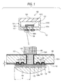
- Fig. 1 is a typical longitudinal section view of a package 100 using a substrate according to an embodiment 1 of the invention.
- the package 100 is a semiconductor device, which includes a substrate 101 made of Si or the like and, a light emitting element 102 as an optical function element.
- the light emitting element 102 is made of an LED or the like and mounted on the substrate 101.
- the light emitting element 102 includes a base member made of sapphire (A1203), a P layer, an N layer, an electrode and the like.
- the invention can also be applied to, for example, a semiconductor device structured such that a light receiving or an MEMS element is mounted on a substrate.
- a light transmissible flat-plate-shaped cover 103 made of glass or the like.
- a storage portion 101C which is defined by a base 101A for mounting the light emitting element 102 and a wall portion 101B provided on and rising up from the base 101A.
- This storage portion 101C is formed in such a direction that the upper surface side of the substrate 101 is open.
- the upper end of the wall portion 101B formed so as to surround the periphery of the storage portion 101C is connected to the cover 103 to thereby seal the light emitting element 102.
- the light emitting element 102 is mounted in the storage portion 101C which is an airtight sealed closed space. Therefore, the storage portion 101C can be decompressed or can be filled with an inert gas, thereby being able not only to maintain the performance of the light emitting element 102 but also to lengthen the life thereof.
- a space for sealing the light emitting element 102 can be held clean, whereby, preferably, the quality of the light emitting element 102 is excellent.
- the light emitting element 102 is placed on a bump 106 made of Au.
- the bump 106 is electrically connected to a through electrode 107 through a connecting layer 106A.
- the through electrode 107 is formed so as to penetrate through the bottom surface of the substrate 101.
- the through electrode 107 is produced by growing Cu or Ni in a cylindrical space within the through hole 120 according to an electrolytic plating method.
- the connecting layer 106A includes a Ni layer and an Au layer superimposed on top of each other in such a manner that, for example, the Au layer provides a front surface.
- the connecting layer 106A may also be made of a Ni/Pd/Au plated layer (Au provides the front surface thereof), or another plated layer.
- a connecting layer 108A which includes a Ni layer and a Au layer superimposed on top of each other in such a manner that, for example, the Au layer provides the front surface.
- a solder bump 108 In the connecting layer 108A, there is formed a solder bump 108. That is, the formation of the through electrode 107 can facilitate the connection between the light emitting element 102 and the object to be connected existing on the outside of a space where the light emitting element 102 is sealed up. Also, between the solder bump 108 and through electrode 107, there may also be formed a connecting layer composed of, for example, a Ni/Au plated layer; however, it is omitted in Fig. 1 .
- an insulating layer 110 insulates the substrate 101 and through electrode 107 from each other as well as the substrate 101 and bump 106 from each other.
- a seal structure which seals not only a through hole 120 penetrating through the base 101A of the substrate 101 but also the through electrode 107 formed in the through hole 120.
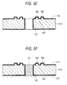
- a portion which is shown in an enlarged manner, provides the seal structure 130 of the through electrode 107.
- the seal structure 130 not only prevents the open air from flowing into the storage portion 101C through such clearance but also prevents an inert gas pressed by the storage portion 101C from leaking to the outside.
- the seal structure 130 includes an uneven portion 140 formed on the lower surface of the base 101A, a contact layer 150 formed on the surface of the uneven portion 140, a power supply layer 160, and an electrode layer 170 formed on the surface of the power supply layer 160.
- the uneven portion 140 includes a first recessed portion 180 formed at a position spaced by a distance L1 (for example, 10 ⁇ m ⁇ 100 ⁇ m) in the radial direction from the outer periphery of the through electrode 107 or from the inner wall of the through hole 120, and a second recessed portion 190 formed at a position spaced further by a given distance L2 (for example, 10 ⁇ m - 100 ⁇ m) from the first recessed portion 180.
- a distance L1 for example, 10 ⁇ m ⁇ 100 ⁇ m
- a projecting portion 200 between the first and second recessed portions 180 and 190, there is formed a projecting portion 200.
- the radial direction width L3 (for example, 10 ⁇ m - 100 ⁇ m) of the projecting portion 200 is equal to an interval (a spaced distance) between the first and second recessed portion 180 and 190.
- the respective distances L1, L2 and L3 are set equal to each other; however, these distances may also be set different from each other and the respective portions may also be disposed at irregular intervals.
- the connecting distance is extended by the number of step portions of the first and second recessed portions 180 and 190 than the radius R of the electrode 170, not only the connecting strength between the base 101A and electrode 170 is increased but also airtightness on the lower surface of the base 101A is enhanced greatly.
- the depth H of the first and second recessed portions 180 and 190 is set for a given value (for example, 1 ⁇ m - 50 ⁇ m) which corresponds to the radius R of the electrode layer 170 or the inside diameter of the through hole 120.
- the depths H of the first and second recessed portions 180 and 190 may be set equal to each other or may be set different from each other.
- the positions and depths in the radial direction of the first and second recessed portions 180 and 190 are not limited to the above-mentioned numeral values that have been shown within the parentheses, but they may be respectively set for numeral values which are selected optionally according to the diameter of the through electrode 107 (the inside diameter of the through hole 120), the thickness of the substrate 101 or the base 101A, or the like.
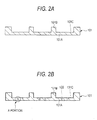
- the upper surface side of the substrate 101 which is made of Si or the like, is etched and patterned to thereby form the storage portion 101C for installing the light emitting element 102 (see Fig. 1 ).
- description will be given of a manufacturing method for etching the upper surface side of the substrate 101 to thereby form the storage portion 101C for storing the light emitting element 102; however, when the substrate 101 is small in thickness, there may also be employed a manufacturing method in which a wall for surrounding the periphery of the light emitting element 102 is formed on the surface of a substrate formed in a flat plate shape to thereby form a storage portion.
- the through hole 120 for forming the through electrode 107 is formed according to an etching operation in such a manner that the through hole 120 penetrates through the base 101A of the substrate 101 in the vertical direction thereof.
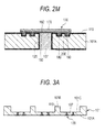
- description will be given below of steps of forming the seal structure 130 in the A portion that is shown in Fig. 2B so as to surround not only the through hole 120 but also its peripheral portion.
- a resist 210 such as a dry film resist is formed on the surface 101D of the lower surface side (in Fig. 2C , for convenience of explanation, the lower direction is shown in a reversed manner) of the base 101A.
- the resist 210 is patterned (exposed and developed) and to thereby remove the portions thereof that correspond to the forming positions of the above-mentioned first and second recessed portions 180 and 190.
- Openings 212 and 214 which are formed in the resist 210 according to the patterning operation, respectively correspond to the outline shapes of the first and second recessed portions 180 and 190.
- the openings 212 and 214 are respectively formed at positions spaced in the radial direction by given distances from the through hole 120 in a concentric circle shape or in a square shape with the through hole 120 as the center thereof in such a manner as to surround the through hole 120.
- an etching processing is enforced on the surface 101D of the base 101A that is exposed to the openings 212 and 214 of the resist 210 formed through the above-mentioned patterned processing, thereby forming ring-shaped grooves (ring shape when viewed from above) or square-frame-shaped grooves (square shape when viewed from above) respectively composed of the first and second recessed portions 180 and 190.
- the etching processing is enforced in such a manner that the surface of the upper surface side of the base 101A is masked by the resist 210 or the like, on the surface 101D of the base 101A, there are etched and formed such first and second recessed portions 180 and 190 that correspond in shape to the patterned shapes (shapes when viewed from above) of the openings 212 and 214. Therefore, by changing the dimensions and intervals of the openings 212 and 214 of the resist 210, the first and second recessed portions 180 and 190 can be formed in arbitrary dimensions and intervals.
- the resist 210 is swollen and softened using a release solution and is then brushed, whereby the resist 210 is removed.
- a substrate 101 in which, on the surface 101D of the base 101A, there are formed a first recessed portion 180, a second recessed portion 190 and a projecting portion 200 respectively having a concentric circle shape or a square frame shape in such a manner that they surround the periphery of the through hole 120.
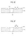
- an insulting layer 110 which is composed of an oxide film (which is also referred to as a silicone oxide film or a thermal oxide film).
- a conductive tape 220 (which is shown by a one-dot chained line in Fig. 2H ) is bonded onto the lower surface side of the base 101A of the substrate 101. And, with the conductive tape 220 as a power supply layer, there is grown a Cu layer or a Ni layer in the through hole 120 according to an electrolytic plating method or the like. Owing to this, in the through hole 120, there is formed a through electrode 107 which is obtained by depositing Cu or Ni. And, after the formation of the through electrode 107, the conductive tape 220 is peeled and removed from the lower surface of the base 101A.
- a close contact metal for example, Ti, Ta or Cr
- a close contact metal having a good close contact property with respect to the insulating layer 110 is deposited on the entire surface 101D of the base 101A including the first recessed portion 180, second recessed portion 190, projecting portion 200 and through electrode 107 to thereby form a close contact layer 150 on the surface 101D.
- the surface of the close contact layer 150 has a distance which is the sum of the radial direction (peripheral direction) length from the inner wall of the through hole 120 (or the outer periphery of the through electrode 107) to the peripheral edge portion of the substrate and the depths (or the heights) of the first recessed portion 180, second recessed portion 190 and projecting portion 200 in the vertical direction. Since the close contact layer 150 is connected to the surfaces (including the radial direction and vertical direction wall surfaces) of the first recessed portion 180, second recessed portion 190, and projecting portion 200 in this manner, the close contact between the close contact layer 150 and insulating layer 110 is enhanced, whereby the close contact layer 150 can be firmly placed on top of the insulating layer 110.
- a power supply layer 160 made of, for example, Cu is formed on the surface of the close contact layer 150. Since the power supply layer 160 is connected not only to the close contact layer 150 having a high close contact property but also to the surfaces (including the vertical direction wall surfaces) of the first recessed portion 180, second recessed portion 190 and projecting portion 200, the connecting distance thereof is extended greatly when compared with a case where it is connected to a flat surface to thereby enhance the degree of the close contact between the close contact layer 150 and power supply layer 160, so that the power supply layer 160 can be placed onto the close contact layer 150 firmly.
- a resist 230 is formed on the surface of the power supply layer 160, and the resist 230 is patterned (exposed and developed) to remove the portion thereof that corresponds to the forming position of the above-mentioned electrode layer 170, thereby forming an electrode forming opening 232.
- the electrode forming opening 232 is formed in a circular or square shape with the axis of the through electrode 107 as a center thereof in such a manner that the first recessed portion 180, second recessed portion 190 and projecting portion 200 are exposed.
- an electrolytic plating processing is enforced on the surface of the power supply layer 160 by supplying power from the power supply layer 160 according to a semi-additive method, whereby an electrode layer 170 made of a Cu plated layer is formed on the surface of the power supply layer 160.
- the electrode layer 170 may also be formed by other methods such as a subtractive method than the semi-additive method.
- the electrode layer 170 is connected to the surfaces of the first recessed portion 180, second recessed portion 190 and projecting portion 200 through the insulating layer 110, close contact layer 150 and power supply layer 160, the close contact between the electrode layer 170 and the base 101A is enhanced, whereby the electrode layer 170 can be placed on top of the base 101A firmly.
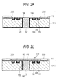
- the resist 230 is removed and, after then, by etching, there are removed the close contact layer 150 and power supply layer 160 except for a portion which exist in the area of the electrode layer 170 (the outside area of the electrode layer 170). This completes the seal structure 130 shown in Fig. 1 .
- the seal structure 130 is structured such that the insulating layer 110, close contact layer 150, power supply layer 160 and electrode layer 170 are placed on the surfaces (including the vertical direction wall surfaces) of the first recessed portion 180, second recessed portion 190 and projecting portion 200. Therefore, even when there is generated a small clearance between the inner wall of the through hole 120 and the outer periphery of the through electrode 107, the airtightness of the periphery of the through electrode 107 can be enhanced as well as the connecting strength can be enhanced when compared with a flat surface structure.
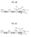
- connecting layers 106A and 108A which are respectively made of Ni/Au or the like.
- the connecting layers 106A are respectively formed on the upper end side (on the storage portion 101C side) of the corresponding through electrodes 107.
- the connecting layers 108A are respectively formed on the opposite side (on the lower end side) of the corresponding through electrodes 107.
- each of the connecting layers 106A there is formed a bump 106 by bonding a wire made of Au or the like to the connecting layer 106A.
- a wire made of Au or the like By the way, in Fig. 3C and its following figures, the illustration of the connecting layers 106A is omitted.
- the insulating layers 110 formed on the upper end side surface of the wall portions 101B in the periphery of the storage portion 101C are removed according to a mask etching method or the like.
- a mask etching method or the like for the insulating layer 110 formed on the upper end side surface of the wall portions 101B in the periphery of the storage portion 101C.
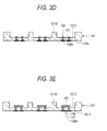
- a light emitting element 102 is disposed within each of the storage portions 101C.
- the electrode of the light emitting element 102 and bump 106 are electrically connected together, whereby the light emitting element 102 and through electrode 107 can be electrically connected together through the bump 106.
- a flat-plate-shaped light transmissible cover 103 made of borosilicate glass or the like is connected to the upper end face of the wall portion 101B of the substrate 101 according to an anode bonding method or the like, thereby forming a structure which seals the light emitting element 102 within the storage portion 101C of the substrate 101.
- anode bonding method there is applied a high voltage into between the cover 103 and substrate 101 to increase the temperatures of the cover 103 and substrate 101, thereby connecting together the cover 103 and the upper end face of the wall portion 101B.
- Si constituting the substrate and oxygen contained in the glass forming the cover are united together, resulting in the connection that is stable and has a good connecting force. Also, differently from the connection that is obtained using resin material, there is little possibility of generation of such gas or impurities that contaminate the space for sealing the light emitting element 102.
- a solder bump 108 is formed in the connecting layer 108A.
- the substrate 101 and cover 103 are diced and cut off into individual pieces, thereby completing the above-mentioned packages 100 (see Fig. 1 ).
- Fig. 4 is a longitudinal section view which typically shows a seal structure used in a substrate according to an embodiment 2 of the invention. Description will be given below of the embodiment 2 of the seal structure used in the package 100 with reference to Fig. 4 .
- the same parts as those that have been described hereinbefore are given the same designations and thus, in some cases, the description thereof will be omitted.
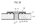
- a seal structure 330 includes an uneven portion 340 formed on the lower side surface of the base 101A, a close contact layer 150 formed on the surface of the uneven portion 340, a power supply layer 160 formed on the close contact layer 150 and an electrode layer 170 formed on the surface of the power supply layer 160.
- the uneven portion 340 includes a first projecting portion 380 formed at a position spaced by a given distance L1 (for example, 10 ⁇ m - 100 ⁇ m) in the radial direction with respect to the outer periphery of the through electrode 107 or the inner wall of the through hole 120, and a second projecting portion 390 formed at a position spaced by a given distance L2 (for example, 10 ⁇ m - 100 ⁇ m) further outwardly from the first projecting portion 380.
- a given distance L1 for example, 10 ⁇ m - 100 ⁇ m
- L2 for example, 10 ⁇ m - 100 ⁇ m
- a recessed portion 400 between the first and second projecting portions 380 and 390, there is formed a recessed portion 400.
- the width L3 (for example, 10 ⁇ m - 100 ⁇ m) in the radial direction of the recessed portion 400 is equal to the interval (spaced distance) between the first and second projecting portions 380 and 390.
- the respective distances L1, L2 and L3 are set to be equal to each other. However, they may also be set different from each other and thus the projecting and recessed portions may also be disposed at irregular intervals.
- the heights H of the first and second projecting portions 380 and 390 are respectively set for given values ((for example, 1 ⁇ m ⁇ 10 ⁇ m) which correspond to the radius R of the electrode layer 170 or the inside diameter of the through hole 120.
- the heights H of the first and second projecting portions 380 and 390 may be set equal to each other or may be set different from each other.
- the radial-direction positions of the first and second projecting portions 380, 390 as well as the heights thereof are not limited to the numerical values that are stated in the above-mentioned parentheses but may be set for arbitrary values depending on the diameter of the through electrode 107 (the inside diameter of the through hole 120), the thickness of the substrate 101 or base 101A, and the like.
- a resist 210 which is made of a dry film resist or the like.
- the resist 210 is patterned (exposed and developed) and is thus removed from the other portions of the surface 101D than the portions thereof corresponding to the forming positions of the above-mentioned first and second projecting portions 380 and 390, whereby the resist 210 is left only in the portions that correspond to the forming portions of the first and second projecting portions 380 and 390.
- the patterns of the resists 210 left on the surface 101D of the base 101A respectively correspond to the outer shapes of the first and second projecting portions 380 and 390.
- these patterns are respectively formed at positions spaced in the radial direction by a given distance from the through hole 120, while they have a concentric circle shape or a square frame shape with the through hole 120 as the center thereof in such a manner that they surround the through hole 120.
- a step shown in Fig. 5C there is enforced an etching processing on the surface 101D of the base 101A exposed in openings 216, 217 and 218 which are respectively formed between the patterned resists 210. Owing to this, the portions of the surface 101D that the resists 210 are not formed on are removed. As a result of this, there are formed a ring-shaped projecting portion (a ring shape when viewed from above) or a square-frame-shaped projecting portion (a square shape when viewed from above) which is composed of the first and second projecting portions 380 and 390, and a recessed portion 400.
- the etching processing is enforced in such a state where the upper surface side surface of the base 101A is masked by the resists 210 or the like.
- the periphery of the through hole 120 and the recessed portion 400 situated outside such periphery both of which correspond to the pattern shapes (when viewed from above) of the openings 216, 217 and 218 of the resists 210. Therefore, by changing the respective dimensions of the openings 216, 217 and 218 of the resists 210 and the spaced distances thereof, the first and second projecting portions 380 and 390 can be formed in arbitrary dimensions and at arbitrary intervals.
- the resists 210 are swollen and softened using a release solution and, after then they are brushed, whereby the resists 210 are removed.
- a substrate 101 structured such that, on the surface 101D of the base 101A, there are formed the first projecting portion 380, second projecting portion 390 and recessed portion 400 respectively having a concentric circle shape or a square frame shape in such a manner as to surround the periphery of the through hole 120.
- an insulating layer 110 made of an oxide film (which is also referred to as a silicone oxide film or a thermal oxide film) according to a thermal CVD method or the like.
- a conductive tape 220 (which is shown by a one-dot chained line in Fig. 5F ) is bonded to, for example, the lower surface side of the base 101A of the substrate 101. And, with the conductive tape 220 as the power supply layer, there is grown a Cu layer or a Ni layer in the through hole 120 according to an electrolytic plating method. As a result of this, in the through hole 120, there is provided a through electrode 107 that is obtained through the deposition of Cu or Ni. After provision of the through electrode 107 in the through hole 120, the conductive tape 220 is separated and removed from the lower surface of the base 101A.
- a close contact metal for example, Ti, Ta, Cr or the like
- a close contact metal having a good close contact property with respect to the insulating layer 110 is deposited on the entire surface of the base 101A including the surfaces of the first projecting portion 380, second projecting portion 390, recessed portion 400 and through electrode 107 to thereby form a close contact layer 150 thereon.
- the surface of the close contact layer 150 has a distance corresponding to the sum of a radial direction (peripheral direction) length from the inner wall of the through hole 120 (or the outer periphery of the through electrode 107) to the peripheral edge surface of the substrate and the vertical direction depths (or heights) of the first projecting portion 380, second projecting portion 390 and recessed portion 400. That is, since the close contact layer 150 is connected to the surfaces (including the radial direction and vertical direction wall surfaces) of the first projecting portion 380, second projecting portion 390 and recessed portion 400 in this manner, the airtightness between the close contact layer 150 and insulating layer 110 is enhanced, whereby the close contact layer 150 can be formed firmly on the insulating layer 110.
- a power supply layer 160 which is made of Cu or the like. Since the power supply layer 160 is sealed not only to the close contact layer 150 having a high close contact property but also to the surfaces (including the vertical direction wall surfaces) the first projecting portion 380, second projecting portion 390 and recessed portion 400, the connecting distance of the power supply layer 160 is extended greatly when compared with a case where it is connected to a flat surface. Owing to this, the airtightness between the close contact layer 150 and power supply layer 160 is enhanced, and thus the power supply layer 160 can be firmly formed on the close contact layer 150.
- a plated resist 230 on the surface of the power supply layer 160; and then, the plated resist 230 is patterned (exposed and developed) to remove the portion of the plated resist 230 that corresponds to the forming portion of the above-mentioned electrode layer 170, thereby forming an electrode layer forming opening 232.
- the electrode layer forming opening 232 is formed in a circular or square shape (when viewed from above) with the axis of the through electrode 107 as the center thereof in order that the first projecting portion 380, second projecting portion 390 and recessed portion 400 can be exposed.
- the electrode layer 170 which is made of a Cu plated layer.
- the electrode layer 170 may also be formed according to other methods such as a subtractive method than the semi-additive method.
- the connecting distance thereof is extended greatly when compared with a case where it is connected to a flat surface. Owing to this, the airtightness between the electrode layer 170 and power supply layer 160 is enhanced, and thus the electrode layer 170 can be firmly formed on the power supply layer 160.
- the resist 230 is removed and, next, the close contact layer 150 and power supply layer 160 existing in the other portion of the electrode layer 170 (the outer portion of the electrode layer 170) than the lower portion thereof are removed by etching. This completes the seal structure 330 shown in Fig. 4 .
- the insulating layer 110, close contact layer 150, power supply layer 160 and electrode layer 170 are formed on top of each other on the surfaces (including the wall surfaces in the vertical direction) of the first projecting portion 380, second projecting portion 390 and recessed portion 400. Therefore, even when there is generated a fine clearance between the inner wall of the through hole 120 and the outer periphery of the through electrode 107, not only the airtightness in the periphery of the through electrode 107 can be enhanced but also the connecting strength can be enhanced more when compared with a case where a flat surface is used.
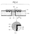
- Fig. 6 is a longitudinal section view which typically shows a seal structure used in a substrate according to an embodiment 3 of the invention. Now, description will be given below of the embodiment 3 of a seal structure used in the package 100 with reference to Fig. 6 .
- the same parts as those that have been described hereinbefore are given the same designations and thus, in some cases, the description thereof will be omitted.
- a rough surface 440 which is composed of a small uneven portion.
- the step shown in Fig. 2B according to the above-mentioned embodiment 1 after the base 101A of the substrate 101 is etched to thereby form the through hole 120 which penetrates through the base 101A in the vertical direction thereof, the entire surface of the inner wall of the through hole 120 or a portion (opening end side) of the inner wall of the through hole 120 is half etched, that is, a roughening processing is enforced on the base 101A.
- an insulating layer 110, a close contact layer 150 and a power supply layer 160 are respectively formed on the entire surface of the base 101A and the inner wall (including the rough surface 440) of the through hole 120, and an electrode layer 170 is formed on the electrode layer forming opening 232 of the resist 230. Also, when forming a through electrode 107 according to the step shown in Fig.
- the through electrode 107 in such a manner that, by shortening the electrolytic plating time, one end of the through electrode 107 is situated lower than the opening end of the through hole 120 so as to allow the exposure of the inner wall of the one end side of the opening of the through hole 120.
- the close contact layer 150 may be formed on the surface of the rough surface 440 with a uniform film thickness.
- This close contact layer 150 may be preferably formed according to, for example, an ALD (Atomic Layer Deposition) method which is capable of forming a uniform thin film at a molecular level.
- ALD Advanced Deposition
- the close contact layer 150 including a small uneven portion preferably, there may be formed such a power supply layer 160 that has a uniform film thickness.
- an electrolytic plating processing according to a semi-additive method by supplying power from the power supply layer 160 to thereby form an electrode layer 170 made of a Cu plated layer on the surface of the power supply layer 160.
- the electrode layer 170 may also be formed according to other methods such as a subtractive method than the semi-additive method.
- the electrode layer 170 not only is formed on the first and second recessed portions 180 and 190 according to the embodiment 1 (or on the first and second projecting portions 380 and 390 according to the embodiment 2) but also is connected through the close contact layer 150 and power supply layer 160 to the surface of the rough surface 440 which is formed on the inner wall of the one end side of the opening of the through hole 120 and includes the small uneven portion. Therefore, the airtightness between the electrode layer 170 and power supply layer 160 is enhanced and thus the electrode layer 170 can be firmly formed on the power supply layer 160.
- the embodiment 3 not only the rough surface 440 but also the first and second recessed portions 180 and 190 according to the embodiment 1 or the first and second projecting portions 380 and 390 according to the embodiment 2 are combined with the inner wall of the through hole 120. Owing to this, the airtightness between the close contact layer 150, power supply layer 160 and electrode layer 170 can be further enhanced than the previously-mentioned embodiments 1 and 2 and thus the electrode layer 170 can be firmly formed on the base 101A.
- first and second recessed portions 180 and 190 or the first and second projecting portions 380 and 390 may also be formed on the upper surface side and lower surface side of the substrate 101 (on both sides of the through electrode 107).
- the rough surface 440 according to the embodiment 3 may also be formed on the opening inner walls on both sides of the through electrode 107; and, the electrode layer 170 may also be formed on the rough surface 440 through the insulating layer 110, close contact layer 150 and power supply layer 160.
- the through electrode 107 is provided on the substrate 101 in which the light emitting element 102 is mounted.
- the invention is not limited to this but, for example, there may also be employed a structure in which the through electrode 107 is provided on a silicone substrate including an integrated circuit, the rough surface 440 is formed in the seal structure 130 according to the embodiment 1, or in the seal structure 330 according to the embodiment 2, or in the inner wall of the opening of the through hole 120, and the electrode layer 170 is formed on the rough surface 440 through the insulating layer 110, close contact layer 150 and power supply layer 160.
- the uneven portion 140 is formed after the through hole 120 is formed, and then the through electrode 107 is formed.
- the invention is not limited to this.
Landscapes
- Engineering & Computer Science (AREA)
- Microelectronics & Electronic Packaging (AREA)
- Computer Hardware Design (AREA)
- Power Engineering (AREA)
- Physics & Mathematics (AREA)
- Condensed Matter Physics & Semiconductors (AREA)
- General Physics & Mathematics (AREA)
- Ceramic Engineering (AREA)
- Manufacturing & Machinery (AREA)
- Led Device Packages (AREA)
- Led Devices (AREA)
Abstract
Description
- This application claims priority to Japanese Patent Application No.
2007-097614, filed April 3, 2007 2007-097614 - The present disclosure relates to a substrate and a method for manufacturing the substrate. Specifically, the invention relates to a substrate which is used in a package to be airtight sealed and includes a through electrode, and to a method for manufacturing the substrate.
- As an element which is formed or mounted on a substrate, there are available various kinds of elements. Some kinds of elements may preferably be used in such a manner that they are sealed on the substrate.
- For example, an optical function element such as an LED (Light Emitting Diode), or an element (which is hereinafter referred to as a MEMS element) using a micro electro mechanical system (which is also referred to as MEMS) has a fine and delicate structure; and, therefore, when such element is used on the substrate, structurally, it may preferably be used in such a manner that it is sealed.
- As this type of element, besides the optical function element, there are available a pressure sensor, an acceleration sensor, a gyro, and the like. This type of element may preferably be used in a vacuum state or in a reduced pressure state, or in an atmosphere displaced by inert gas; and, it may preferably be stored in a space sealed by such seal structure that is free from the open air and dust contained in the open air.
- As a method for manufacturing an airtight sealed package of this type, there is proposed a method which seals a semiconductor element by putting together silicone wafers (for example, see the Japanese Patent Application Publication No.
2005-19966 - On the other hand, in the above-mentioned package using the airtight sealed structure, it is structured such that the electrode of an element is connected to a through electrode penetrating through a silicone substrate (which is hereinafter referred to as a substrate) to provide an electrical connection between them, whereby the size and thickness of the package can be reduced.
- Also, in a package including a through electrode, when close contact property between the through electrode and an insulating layer formed on the inner wall of the through hole of the substrate is reduced or deteriorated, there is a fear that the open air can flow from the through hole into a space which is airtight sealed. As means for preventing such reduction of the airtight performance in the through hole, for example, there is known a method in which a conductive layer is formed on the end portion of the through electrode formed in the through hole and on the surface of the substrate existing in the periphery of the through electrode to secure the airtight performance owing to the close contact between the conductive layer and the surface of the substrate (for example, see Japanese Patent Application Publication No.
2005-11987 - However, in the above-mentioned method, in order to secure close contact between the conductive layer and the surface of the substrate, it is necessary to increase the size of the conductive layer in the radial direction with the through electrode as a center thereof, which results in the increased size of the package itself.
Also, as the distance between the mutually adjoining through electrodes decreases with the reduced sizes of the respective elements, a space for installation of the conductive layer is limited accordingly, which makes it difficult to secure sufficient airtight performance. - The problems in the art are at least partly overcome by the method for manufacturing a substrate according to Claim 1 and a substrate according to Claim 10.
- Exemplary embodiments of the present invention provide a substrate and a method for manufacturing such substrate.
Exemplary embodiments of the present invention has the following means. - Specifically, according to the invention, a method for manufacturing a substrate having a through electrode formed in at least a portion of a through hole, comprises the steps of:
- forming, on a surface of the substrate situated in the periphery of a portion where the through hole is formed or will be formed, an uneven portion including at least one of a recessed portion and a projecting portion; and,
- forming an electrode layer on a surface of the uneven portion.
- The uneven portion may include at least a plurality of recessed portions or a plurality of projecting portions, and the plurality of recessed portions or the plurality of projecting portions may be formed in a peripheral direction of the substrate at positions different from each other with respect to the center of the through hole.
- The method for manufacturing a substrate may further comprise a step of: forming a close contact layer having a close contact property and a conductive property on the surface of the uneven portion.
The method for manufacturing a substrate may further comprise a step of: forming the through electrode in the portion of the through hole, wherein the electrode layer is formed on an end portion of the through electrode in the through hole.
The method for manufacturing a substrate may further comprise a step of: performing a roughening processing on an inner wall of the through hole.
The method for manufacturing a substrate may further comprise a step of: forming a close contact layer having a close contact property and a conductive property on the inner wall of the through hole and on the surface of the uneven portion.
The method for manufacturing a substrate may further comprise a step of: forming the through hole in the substrate, wherein the through hole is formed before the uneven portion is formed.
The method for manufacturing a substrate may further comprise a step of: forming the through hole in the substrate, wherein the through hole and the uneven portion are formed at the same time. - According to the invention, the uneven portion including at least a recessed portion or a projecting portion is formed on the surface of the substrate situated in the periphery of the through hole; and, the electrode layer is formed on the surface of the uneven portion. Therefore, since the connecting distance between the surface of the substrate and electrode layer can be substantially extended according to the shape of the recessed portion or projecting portion, not only the airtightness in the periphery of the through electrode can be enhanced further but also, even when the space for installation of the electrode layer is small, proper airtightness can be secured. Thus, the invention is also able to cope with the reduced size of the package.
According to another aspect of the present invention a substrate is provided comprising a through electrode formed in at least a portion of a through hole formed in the substrate; an uneven portion formed on a surface of the substrate in the periphery of the through electrode, and including at least one of a recessed portion and a projecting portion; and an electrode layer formed on a surface of the uneven portion.
The uneven portion may be formed in such a manner that it surrounds the periphery of the through electrode.
The uneven portion may include at least a plurality of recessed portions or a plurality of projecting portions, and the plurality of recessed portions or the plurality of projecting portions are formed in a peripheral direction of the substrate at positions different from each other with respect to the center of the through electrode.
The substrate may further comprise: a close contact layer which is formed on the surface of the uneven portion and has a close contact property and a conductive property.
According to the invention at least a portion of an inner wall of the through hole may have a rough surface having a small uneven portion.
The substrate may further comprise a close contact layer which is formed on the inner wall of the through hole and on the surface of the uneven portion and has a close contact property and a conductive property.
According to the invention a substrate includes a storage portion which is defined by a base for mounting a light emitting element and a wall portion standing up on and from the base.
A package is structured such that the upper end of the wall portion so formed as to surround the periphery of the storage portion is connected to a cover to thereby seal a light emitting element.
A seal structure is composed of an uneven portion formed on the lower surface side surface of the base, a close contact layer formed on the surface of the uneven portion, a power supply layer formed on the close contact layer, and an electrode layer formed on the surface of the power supply layer.
The uneven portion includes a first recessed portion formed at a position spaced in the radial direction from the outer periphery of a through electrode or from the inner wall of a through hole, and a second recessed portion formed at a position spaced further outwardly from the first recessed portion.
Other features and advantages may be apparent from the following detailed description, the accompanying drawings and the claims. - Embodiments of the present invention are depicted in the drawings and will be described in more detail in the following. Therein:
-
Fig. 1 is a typical longitudinal section view of apackage 100 using a substrate according to an embodiment 1 of the invention. -
Fig. 2A is an explanatory view of one of steps (step 1) of a method for manufacturing the substrate according to the embodiment 1. -
Fig. 2B is an explanatory view of one of steps (step 2) of the method for manufacturing the substrate according to the embodiment 1. -
Fig. 2C is an explanatory view of one of steps of (step 3) of the method for manufacturing the substrate according to the embodiment 1. -
Fig. 2D is an explanatory view of one of steps (step 4) of a method for manufacturing the substrate according to the embodiment 1. -
Fig. 2E is an explanatory view of one of steps (step 5) of the method for manufacturing the substrate according to the embodiment 1. -
Fig. 2F is an explanatory view of one of steps (step 6) of the method for manufacturing the substrate according to the embodiment 1. -
Fig. 2G is an explanatory view of one of steps (step 7) of the method for manufacturing the substrate according to the embodiment 1. -
Fig. 2H is an explanatory view of one of steps (step 8) of the method for manufacturing the substrate according to the embodiment 1. -
Fig. 2I is an explanatory view of one of steps (step 9) of the method for manufacturing the substrate according to the embodiment 1. -
Fig. 2J is an explanatory view of one of steps (step 10) of the method for manufacturing the substrate according to the embodiment 1. -
Fig. 2K is an explanatory view of one of steps (step 11) of the method for manufacturing the substrate according to the embodiment 1. -
Fig. 2L is an explanatory view of one of steps (step 12) of the method for manufacturing the substrate according to the embodiment 1. -
Fig. 2M is an explanatory view of one of steps (step 13) of the method for manufacturing the substrate according to the embodiment 1. -
Fig. 3A is an explanatory view of one of steps (step 1) of a method for mounting a light emitting element into the substrate according to the embodiment 1. -
Fig. 3B is an explanatory view of one of steps (step 2) of the method for mounting a light emitting element into the substrate according to the embodiment 1. -
Fig. 3C is an explanatory view of one of steps (step 3) of the method for mounting a light emitting element into the substrate according to the embodiment 1. -
Fig. 3D is an explanatory view of one of steps (step 4) of the method for mounting a light emitting element into the substrate according to the embodiment 1. -
Fig. 3E is an explanatory view of one of steps (step 5) of the method for mounting a light emitting element into the substrate according to the embodiment 1. -
Fig. 3F is an explanatory view of one of steps (step 6) of the method for mounting a light emitting element into the substrate according to the embodiment 1. -
Fig. 3G is an explanatory view of one of steps (step 7) of the method for mounting a light emitting element into the substrate according to the embodiment 1. -
Fig. 3H is an explanatory view of one of steps (step 8) of the method for mounting a light emitting element into the substrate according to the embodiment 1. -
Fig. 4 is a typical longitudinal section view of a seal structure used in a substrate according to an embodiment 2. -
Fig. 5A is an explanatory view of one of steps (step 1) of a method for manufacturing the substrate according to the embodiment 2. -
Fig. 5B is an explanatory view of one of steps (step 2) of the method for manufacturing the substrate according to the embodiment 2. -
Fig. 5C is an explanatory view of one of steps (step 3) of the method for manufacturing the substrate according to the embodiment 2. -
Fig. 5D is an explanatory view of one of steps (step 4) of the method for manufacturing the substrate according to the embodiment 2. -
Fig. 5E is an explanatory view of one of steps (step 5) of the method for manufacturing the substrate according to the embodiment 2. -
Fig. 5F is an explanatory view of one of steps (step 6) of the method for manufacturing the substrate according to the embodiment 2. -
Fig. 5G is an explanatory view of one of steps (step 7) of the method for manufacturing the substrate according to the embodiment 2. -
Fig. 5H is an explanatory view of one of steps (step 8) of the method for manufacturing the substrate according to the embodiment 2. -
Fig. 5I is an explanatory view of one of steps (step 9) of the method for manufacturing the substrate according to the embodiment 2. -
Fig. 5J is an explanatory view of one of steps (step 10) of the method for manufacturing the substrate according to the embodiment 2. -
Fig. 5K is an explanatory view of one of steps (step 11) of the method for manufacturing the substrate according to the embodiment 2. -
Fig. 6 is a typical longitudinal section view of a seal structure used in a substrate according to an embodiment 3. - Now, description will be given below of the best mode for carrying out the invention with reference to the accompanying drawings.
-
Fig. 1 is a typical longitudinal section view of apackage 100 using a substrate according to an embodiment 1 of the invention. Referring toFig. 1 , thepackage 100 is a semiconductor device, which includes asubstrate 101 made of Si or the like and, alight emitting element 102 as an optical function element. Thelight emitting element 102 is made of an LED or the like and mounted on thesubstrate 101. Thelight emitting element 102 includes a base member made of sapphire (A1203), a P layer, an N layer, an electrode and the like. - By the way, in the present embodiment, although description is given of a structure in which the
light emitting element 102 is mounted on thesubstrate 101, it is not limitative but, of course, the invention can also be applied to, for example, a semiconductor device structured such that a light receiving or an MEMS element is mounted on a substrate. - Also, on the
light emitting element 102, there is placed a light transmissible flat-plate-shapedcover 103 made of glass or the like. - Also, on the
substrate 101, there is provided astorage portion 101C which is defined by abase 101A for mounting thelight emitting element 102 and awall portion 101B provided on and rising up from thebase 101A. Thisstorage portion 101C is formed in such a direction that the upper surface side of thesubstrate 101 is open. And, according to the structure of thepackage 100, the upper end of thewall portion 101B formed so as to surround the periphery of thestorage portion 101C is connected to thecover 103 to thereby seal thelight emitting element 102. Thelight emitting element 102 is mounted in thestorage portion 101C which is an airtight sealed closed space. Therefore, thestorage portion 101C can be decompressed or can be filled with an inert gas, thereby being able not only to maintain the performance of thelight emitting element 102 but also to lengthen the life thereof. - Also, suppose the
substrate 101 and cover 103 are connected together by anode bonding, for example, when compared with they are connected together by organic material such as resin, a space for sealing thelight emitting element 102 can be held clean, whereby, preferably, the quality of thelight emitting element 102 is excellent. - Also, the
light emitting element 102 is placed on abump 106 made of Au. Thebump 106 is electrically connected to a throughelectrode 107 through a connectinglayer 106A. The throughelectrode 107 is formed so as to penetrate through the bottom surface of thesubstrate 101. The throughelectrode 107 is produced by growing Cu or Ni in a cylindrical space within the throughhole 120 according to an electrolytic plating method. The connectinglayer 106A includes a Ni layer and an Au layer superimposed on top of each other in such a manner that, for example, the Au layer provides a front surface. Also, the connectinglayer 106A may also be made of a Ni/Pd/Au plated layer (Au provides the front surface thereof), or another plated layer. - On the opposite side (in
Fig. 1 , the lower end side) of the side of the throughelectrode 107 to which thelight emitting element 102 is connected, there is formed a connectinglayer 108A which includes a Ni layer and a Au layer superimposed on top of each other in such a manner that, for example, the Au layer provides the front surface. In the connectinglayer 108A, there is formed asolder bump 108. That is, the formation of the throughelectrode 107 can facilitate the connection between the light emittingelement 102 and the object to be connected existing on the outside of a space where thelight emitting element 102 is sealed up. Also, between thesolder bump 108 and throughelectrode 107, there may also be formed a connecting layer composed of, for example, a Ni/Au plated layer; however, it is omitted inFig. 1 . - Also, on the lower surface of the
substrate 101, there is formed an insulating layer (silicone oxide film) 110. This insulatinglayer 110 insulates thesubstrate 101 and throughelectrode 107 from each other as well as thesubstrate 101 and bump 106 from each other. - Here, description will be given of a seal structure which seals not only a through
hole 120 penetrating through thebase 101A of thesubstrate 101 but also the throughelectrode 107 formed in the throughhole 120. InFig. 1 , a portion, which is shown in an enlarged manner, provides theseal structure 130 of the throughelectrode 107. When the close contact between the throughelectrode 107, and the insulating layer (silicone oxide film) 110 formed on the inner wall of the throughhole 120 is deteriorated to thereby cause a small clearance, theseal structure 130 not only prevents the open air from flowing into thestorage portion 101C through such clearance but also prevents an inert gas pressed by thestorage portion 101C from leaking to the outside. - The
seal structure 130 includes anuneven portion 140 formed on the lower surface of thebase 101A, acontact layer 150 formed on the surface of theuneven portion 140, apower supply layer 160, and anelectrode layer 170 formed on the surface of thepower supply layer 160. - The
uneven portion 140 includes a first recessedportion 180 formed at a position spaced by a distance L1 (for example, 10 µ m ~ 100 µm) in the radial direction from the outer periphery of the throughelectrode 107 or from the inner wall of the throughhole 120, and a second recessedportion 190 formed at a position spaced further by a given distance L2 (for example, 10 µ m - 100 µ m) from the first recessedportion 180. - Also, between the first and second recessed
portions portion 200. The radial direction width L3 (for example, 10 µm - 100 µm) of the projectingportion 200 is equal to an interval (a spaced distance) between the first and second recessedportion - In this manner, since the first recessed
portion 180, projectingportion 200 and second recessedportion 190 are formed at different positions in the radial direction of the substrate from the outer periphery of the throughelectrode 107 or from the inner wall of the throughhole 120, the connecting length L of thecontact layer 150 with respect to theuneven portion 140 provides a length (L=R+4H) which is the sum of the radius R of theelectrode layer 170 and a product obtained when the length H (the depth of first and second recessedportions 180 and 190) of a step portion in the radial direction and in the vertical direction is multiplied by 4. Therefore, since the connecting distance is extended by the number of step portions of the first and second recessedportions electrode 170, not only the connecting strength between thebase 101A andelectrode 170 is increased but also airtightness on the lower surface of thebase 101A is enhanced greatly. - The depth H of the first and second recessed
portions electrode layer 170 or the inside diameter of the throughhole 120. The depths H of the first and second recessedportions - By the way, the positions and depths in the radial direction of the first and second recessed
portions substrate 101 or thebase 101A, or the like. - Here, description will be given below of an example of a method for manufacturing the
seal structure 130 for use in the above-mentionedpackage 100 with reference toFigs. 2A to 2K , specifically, the steps (1 to 11) of the manufacturing method. However, in these figures, the portions, which have been described above, are given the same reference characters and thus, in some cases, the description thereof will be omitted. - Firstly, in a step shown in
Fig. 2A , the upper surface side of thesubstrate 101, which is made of Si or the like, is etched and patterned to thereby form thestorage portion 101C for installing the light emitting element 102 (seeFig. 1 ). By the way, in the present embodiment, description will be given of a manufacturing method for etching the upper surface side of thesubstrate 101 to thereby form thestorage portion 101C for storing thelight emitting element 102; however, when thesubstrate 101 is small in thickness, there may also be employed a manufacturing method in which a wall for surrounding the periphery of thelight emitting element 102 is formed on the surface of a substrate formed in a flat plate shape to thereby form a storage portion. - Next, in a step shown in
Fig. 2B , the throughhole 120 for forming the throughelectrode 107 is formed according to an etching operation in such a manner that the throughhole 120 penetrates through thebase 101A of thesubstrate 101 in the vertical direction thereof. Referring to the operation to be executed after the present step, description will be given below of steps of forming theseal structure 130 in the A portion that is shown inFig. 2B so as to surround not only the throughhole 120 but also its peripheral portion. - Next, in a step shown in
Fig. 2C , a resist 210 such as a dry film resist is formed on thesurface 101D of the lower surface side (inFig. 2C , for convenience of explanation, the lower direction is shown in a reversed manner) of thebase 101A. - Next, in a step shown in
Fig. 2D , the resist 210 is patterned (exposed and developed) and to thereby remove the portions thereof that correspond to the forming positions of the above-mentioned first and second recessedportions Openings portions openings hole 120 in a concentric circle shape or in a square shape with the throughhole 120 as the center thereof in such a manner as to surround the throughhole 120. - Next, in a step shown in
Fig. 2E , an etching processing is enforced on thesurface 101D of thebase 101A that is exposed to theopenings portions base 101A is masked by the resist 210 or the like, on thesurface 101D of thebase 101A, there are etched and formed such first and second recessedportions openings openings portions - Next, in a step shown in
Fig. 2F , the resist 210 is swollen and softened using a release solution and is then brushed, whereby the resist 210 is removed. As a result of this, there is produced asubstrate 101 in which, on thesurface 101D of thebase 101A, there are formed a first recessedportion 180, a second recessedportion 190 and a projectingportion 200 respectively having a concentric circle shape or a square frame shape in such a manner that they surround the periphery of the throughhole 120. - Next, in a step shown in
Fig. 2G , on the surface of thesubstrate 101 including the lower surface of thebase 101A (containing the surfaces of the first recessedportion 180, second recessedportion 190 and projecting portion 200), the inner wall surface of thestorage portion 101C and the inner wall surface of the throughhole 120, according to a thermal CVD method or the like, there is formed aninsulting layer 110 which is composed of an oxide film (which is also referred to as a silicone oxide film or a thermal oxide film). - Next, in a step shown in
Fig. 2H , for example, a conductive tape 220 (which is shown by a one-dot chained line inFig. 2H ) is bonded onto the lower surface side of thebase 101A of thesubstrate 101. And, with theconductive tape 220 as a power supply layer, there is grown a Cu layer or a Ni layer in the throughhole 120 according to an electrolytic plating method or the like. Owing to this, in the throughhole 120, there is formed a throughelectrode 107 which is obtained by depositing Cu or Ni. And, after the formation of the throughelectrode 107, theconductive tape 220 is peeled and removed from the lower surface of thebase 101A. - Next, in a step shown in
Fig. 2I , according to a PVD (Physical Vapor Deposition) method or a CVD (Chemical Vapor Deposition) method, a close contact metal (for example, Ti, Ta or Cr) having a good close contact property with respect to the insulatinglayer 110 is deposited on theentire surface 101D of thebase 101A including the first recessedportion 180, second recessedportion 190, projectingportion 200 and throughelectrode 107 to thereby form aclose contact layer 150 on thesurface 101D. - Thus, the surface of the
close contact layer 150 has a distance which is the sum of the radial direction (peripheral direction) length from the inner wall of the through hole 120 (or the outer periphery of the through electrode 107) to the peripheral edge portion of the substrate and the depths (or the heights) of the first recessedportion 180, second recessedportion 190 and projectingportion 200 in the vertical direction. Since theclose contact layer 150 is connected to the surfaces (including the radial direction and vertical direction wall surfaces) of the first recessedportion 180, second recessedportion 190, and projectingportion 200 in this manner, the close contact between theclose contact layer 150 and insulatinglayer 110 is enhanced, whereby theclose contact layer 150 can be firmly placed on top of the insulatinglayer 110. - Next, in a step shown in
Fig. 2J , according to the PVD method or an electroless plating method, apower supply layer 160 made of, for example, Cu is formed on the surface of theclose contact layer 150. Since thepower supply layer 160 is connected not only to theclose contact layer 150 having a high close contact property but also to the surfaces (including the vertical direction wall surfaces) of the first recessedportion 180, second recessedportion 190 and projectingportion 200, the connecting distance thereof is extended greatly when compared with a case where it is connected to a flat surface to thereby enhance the degree of the close contact between theclose contact layer 150 andpower supply layer 160, so that thepower supply layer 160 can be placed onto theclose contact layer 150 firmly. - Next, in a step shown in
Fig. 2K , a resist 230 is formed on the surface of thepower supply layer 160, and the resist 230 is patterned (exposed and developed) to remove the portion thereof that corresponds to the forming position of the above-mentionedelectrode layer 170, thereby forming anelectrode forming opening 232. Theelectrode forming opening 232 is formed in a circular or square shape with the axis of the throughelectrode 107 as a center thereof in such a manner that the first recessedportion 180, second recessedportion 190 and projectingportion 200 are exposed. - Next, in a step shown in
Fig. 2L , an electrolytic plating processing is enforced on the surface of thepower supply layer 160 by supplying power from thepower supply layer 160 according to a semi-additive method, whereby anelectrode layer 170 made of a Cu plated layer is formed on the surface of thepower supply layer 160. Also, theelectrode layer 170 may also be formed by other methods such as a subtractive method than the semi-additive method. - Thus, since the
electrode layer 170 is connected to the surfaces of the first recessedportion 180, second recessedportion 190 and projectingportion 200 through the insulatinglayer 110,close contact layer 150 andpower supply layer 160, the close contact between theelectrode layer 170 and thebase 101A is enhanced, whereby theelectrode layer 170 can be placed on top of thebase 101A firmly. - Next, in a step shown in
Fig. 2M , the resist 230 is removed and, after then, by etching, there are removed theclose contact layer 150 andpower supply layer 160 except for a portion which exist in the area of the electrode layer 170 (the outside area of the electrode layer 170). This completes theseal structure 130 shown inFig. 1 . - In this manner, the
seal structure 130 is structured such that the insulatinglayer 110,close contact layer 150,power supply layer 160 andelectrode layer 170 are placed on the surfaces (including the vertical direction wall surfaces) of the first recessedportion 180, second recessedportion 190 and projectingportion 200. Therefore, even when there is generated a small clearance between the inner wall of the throughhole 120 and the outer periphery of the throughelectrode 107, the airtightness of the periphery of the throughelectrode 107 can be enhanced as well as the connecting strength can be enhanced when compared with a flat surface structure. - Now, description will be given below of a procedure (the steps 1 ~ 9 thereof) for mounting the
light emitting element 102 into thestorage portion 101C of thesubstrate 101 having the above-mentionedseal structure 130 with reference toFigs. 3A to 3I . However, in the following figures, the portions, which have been described above, are given the same reference characters and thus, in some cases, the description thereof will be omitted. - Firstly, in a step shown in
Fig. 3A , on the lower surface side of thebase 101A, there are provided airtightness-securedseal structures 130 in the peripheries of the respective throughelectrodes 107 which are respectively disposed in each of a plurality ofstorage portions 101C. - Next, in a step shown in
Fig. 3B , according to a plating method or the like, there are formed connectinglayers layers 106A are respectively formed on the upper end side (on thestorage portion 101C side) of the corresponding throughelectrodes 107. Also, the connectinglayers 108A are respectively formed on the opposite side (on the lower end side) of the corresponding throughelectrodes 107. - Next, in a step shown in
Fig. 3C , on each of the connectinglayers 106A, there is formed abump 106 by bonding a wire made of Au or the like to the connectinglayer 106A. By the way, inFig. 3C and its following figures, the illustration of the connectinglayers 106A is omitted. - Next, in a step shown in
Fig. 3D , the insulatinglayers 110 formed on the upper end side surface of thewall portions 101B in the periphery of thestorage portion 101C are removed according to a mask etching method or the like. To the upper ends of thewall portions 101B, from which the insulatinglayer 110 has been removed in the present step, there can be connected glass-made covers in a step to be executed later. - Next, in a step shown in
Fig. 3E , alight emitting element 102 is disposed within each of thestorage portions 101C. In this case, according to a thermal pressure connection method or an ultrasonic connection method, the electrode of thelight emitting element 102 and bump 106 are electrically connected together, whereby thelight emitting element 102 and throughelectrode 107 can be electrically connected together through thebump 106. - Next, in a step shown in
Fig. 3F , a flat-plate-shaped lighttransmissible cover 103 made of borosilicate glass or the like is connected to the upper end face of thewall portion 101B of thesubstrate 101 according to an anode bonding method or the like, thereby forming a structure which seals thelight emitting element 102 within thestorage portion 101C of thesubstrate 101. In this case, in the anode bonding method, there is applied a high voltage into between thecover 103 andsubstrate 101 to increase the temperatures of thecover 103 andsubstrate 101, thereby connecting together thecover 103 and the upper end face of thewall portion 101B. - Owing to execution of the above-mentioned anode bonding, Si constituting the substrate and oxygen contained in the glass forming the cover are united together, resulting in the connection that is stable and has a good connecting force. Also, differently from the connection that is obtained using resin material, there is little possibility of generation of such gas or impurities that contaminate the space for sealing the
light emitting element 102. - Next, in a step shown in
Fig. 3G , asolder bump 108 is formed in the connectinglayer 108A. - After then, in a step shown in
Fig. 3H , thesubstrate 101 and cover 103 are diced and cut off into individual pieces, thereby completing the above-mentioned packages 100 (seeFig. 1 ). - Now,
Fig. 4 is a longitudinal section view which typically shows a seal structure used in a substrate according to an embodiment 2 of the invention. Description will be given below of the embodiment 2 of the seal structure used in thepackage 100 with reference toFig. 4 . In the following figures, the same parts as those that have been described hereinbefore are given the same designations and thus, in some cases, the description thereof will be omitted. - As shown in
Fig. 4 , aseal structure 330 according to the embodiment 2 includes anuneven portion 340 formed on the lower side surface of thebase 101A, aclose contact layer 150 formed on the surface of theuneven portion 340, apower supply layer 160 formed on theclose contact layer 150 and anelectrode layer 170 formed on the surface of thepower supply layer 160. - The
uneven portion 340 includes a first projectingportion 380 formed at a position spaced by a given distance L1 (for example, 10 µ m - 100 µ m) in the radial direction with respect to the outer periphery of the throughelectrode 107 or the inner wall of the throughhole 120, and a second projectingportion 390 formed at a position spaced by a given distance L2 (for example, 10 µ m - 100 µm) further outwardly from the first projectingportion 380. - Also, between the first and second projecting
portions portion 400. The width L3 (for example, 10 µ m - 100 µ m) in the radial direction of the recessedportion 400 is equal to the interval (spaced distance) between the first and second projectingportions - In this manner, since the first projecting
portion 380, recessedportion 400 and second projectingportion 390 are formed at different positions in the radial direction from the outer periphery of the throughelectrode 107 or the inner wall of the throughhole 120, the connection length L of theclose contact layer 150 with respect to theuneven portion 340 provides the value (L=R+4H) that is obtained as the sum of the radius R of theelectrode layer 170 and the product of four and the length H of the step portions in the radial and vertical directions (the first and second projectingportions 380 and 390). Therefore, the connection length is extended by the number of steps of the first and second projectingportions electrode layer 170. This not only enhances the connection strength between thebase 101A andelectrode layer 170 but also greatly enhances the airtightness of the lower side surface of thebase 101A. - The heights H of the first and second projecting
portions electrode layer 170 or the inside diameter of the throughhole 120. The heights H of the first and second projectingportions - By the way, the radial-direction positions of the first and second projecting
portions substrate 101 orbase 101A, and the like. - Next, description will be given below of the steps (1 to 9) of a method for manufacturing the above-mentioned
seal structure 330 with reference toFigs. 5A to 5I . By the way, the respective steps shown inFigs. 5A to 5I correspond to another embodiments of the steps previously described inFigs. 2C to 2K . In the following figures, the same parts as those that have been described hereinbefore are given the same designations and thus, in some cases, the description thereof will be omitted. - Firstly, in a step shown in
Fig. 5A , on thesurface 101D of the lower surface side (inFig. 5A , for convenience of explanation, the downward direction is shown in a reversed manner) of thebase 101A, there is formed a resist 210 which is made of a dry film resist or the like. - Next, in a step shown in
Fig. 5B , the resist 210 is patterned (exposed and developed) and is thus removed from the other portions of thesurface 101D than the portions thereof corresponding to the forming positions of the above-mentioned first and second projectingportions portions surface 101D of thebase 101A respectively correspond to the outer shapes of the first and second projectingportions hole 120, while they have a concentric circle shape or a square frame shape with the throughhole 120 as the center thereof in such a manner that they surround the throughhole 120. - Next, in a step shown in
Fig. 5C , there is enforced an etching processing on thesurface 101D of thebase 101A exposed inopenings surface 101D that the resists 210 are not formed on are removed. As a result of this, there are formed a ring-shaped projecting portion (a ring shape when viewed from above) or a square-frame-shaped projecting portion (a square shape when viewed from above) which is composed of the first and second projectingportions portion 400. - Actually, the etching processing is enforced in such a state where the upper surface side surface of the
base 101A is masked by the resists 210 or the like. Thus, in the etching processing, there are etched the periphery of the throughhole 120 and the recessedportion 400 situated outside such periphery, both of which correspond to the pattern shapes (when viewed from above) of theopenings openings portions - Next, in a step shown in
Fig. 5D , the resists 210 are swollen and softened using a release solution and, after then they are brushed, whereby the resists 210 are removed. As a result of this, there is obtained asubstrate 101 structured such that, on thesurface 101D of thebase 101A, there are formed the first projectingportion 380, second projectingportion 390 and recessedportion 400 respectively having a concentric circle shape or a square frame shape in such a manner as to surround the periphery of the throughhole 120. - Next, in a step shown in
Fig. 5E , on the lower surface of thebase 101A (including the surfaces of the first projectingportion 380, second projectingportion 390 and recessed portion 400) as well as on the surface of thesubstrate 101 including the inner wall surface of thestorage portion 101C and the inner wall surface of the throughhole 120, there is formed an insulatinglayer 110 made of an oxide film (which is also referred to as a silicone oxide film or a thermal oxide film) according to a thermal CVD method or the like. - Next, in a step shown in
Fig. 5F , a conductive tape 220 (which is shown by a one-dot chained line inFig. 5F ) is bonded to, for example, the lower surface side of thebase 101A of thesubstrate 101. And, with theconductive tape 220 as the power supply layer, there is grown a Cu layer or a Ni layer in the throughhole 120 according to an electrolytic plating method. As a result of this, in the throughhole 120, there is provided a throughelectrode 107 that is obtained through the deposition of Cu or Ni. After provision of the throughelectrode 107 in the throughhole 120, theconductive tape 220 is separated and removed from the lower surface of thebase 101A. - Next, in a step shown in
Fig. 5G , according to a PVD (Physical Vapor Deposition) method or a CVD (Chemical Vapor Deposition) method, a close contact metal (for example, Ti, Ta, Cr or the like) having a good close contact property with respect to the insulatinglayer 110 is deposited on the entire surface of thebase 101A including the surfaces of the first projectingportion 380, second projectingportion 390, recessedportion 400 and throughelectrode 107 to thereby form aclose contact layer 150 thereon.
Thus, the surface of theclose contact layer 150 has a distance corresponding to the sum of a radial direction (peripheral direction) length from the inner wall of the through hole 120 (or the outer periphery of the through electrode 107) to the peripheral edge surface of the substrate and the vertical direction depths (or heights) of the first projectingportion 380, second projectingportion 390 and recessedportion 400. That is, since theclose contact layer 150 is connected to the surfaces (including the radial direction and vertical direction wall surfaces) of the first projectingportion 380, second projectingportion 390 and recessedportion 400 in this manner, the airtightness between theclose contact layer 150 and insulatinglayer 110 is enhanced, whereby theclose contact layer 150 can be formed firmly on the insulatinglayer 110. - Next, in a step shown in
Fig. 5H , according to the PVD method or an electroless plating method, on the surface of theclose contact layer 150, there is formed apower supply layer 160 which is made of Cu or the like. Since thepower supply layer 160 is sealed not only to theclose contact layer 150 having a high close contact property but also to the surfaces (including the vertical direction wall surfaces) the first projectingportion 380, second projectingportion 390 and recessedportion 400, the connecting distance of thepower supply layer 160 is extended greatly when compared with a case where it is connected to a flat surface. Owing to this, the airtightness between theclose contact layer 150 andpower supply layer 160 is enhanced, and thus thepower supply layer 160 can be firmly formed on theclose contact layer 150. - Next, in a step shown in
Fig. 5I , there is formed a plated resist 230 on the surface of thepower supply layer 160; and then, the plated resist 230 is patterned (exposed and developed) to remove the portion of the plated resist 230 that corresponds to the forming portion of the above-mentionedelectrode layer 170, thereby forming an electrodelayer forming opening 232. The electrodelayer forming opening 232 is formed in a circular or square shape (when viewed from above) with the axis of the throughelectrode 107 as the center thereof in order that the first projectingportion 380, second projectingportion 390 and recessedportion 400 can be exposed. - Next, in a step shown in
Fig. 5J , according to a semi-additive method, there is enforced an electrolytic plating using power supply from thepower supply layer 160, whereby, on the surface of thepower supply layer 160, there is formed anelectrode layer 170 which is made of a Cu plated layer. Alternatively, theelectrode layer 170 may also be formed according to other methods such as a subtractive method than the semi-additive method. In this manner, since theelectrode layer 170 is connected through theclose contact layer 150 andpower supply layer 160 to the surfaces of the first projectingportion 380, second projectingportion 390 and recessedportion 400, the connecting distance thereof is extended greatly when compared with a case where it is connected to a flat surface. Owing to this, the airtightness between theelectrode layer 170 andpower supply layer 160 is enhanced, and thus theelectrode layer 170 can be firmly formed on thepower supply layer 160. - Next, in a step shown in
Fig. 5K , the resist 230 is removed and, next, theclose contact layer 150 andpower supply layer 160 existing in the other portion of the electrode layer 170 (the outer portion of the electrode layer 170) than the lower portion thereof are removed by etching. This completes theseal structure 330 shown inFig. 4 . - As described above, in the
seal structure 330, the insulatinglayer 110,close contact layer 150,power supply layer 160 andelectrode layer 170 are formed on top of each other on the surfaces (including the wall surfaces in the vertical direction) of the first projectingportion 380, second projectingportion 390 and recessedportion 400. Therefore, even when there is generated a fine clearance between the inner wall of the throughhole 120 and the outer periphery of the throughelectrode 107, not only the airtightness in the periphery of the throughelectrode 107 can be enhanced but also the connecting strength can be enhanced more when compared with a case where a flat surface is used. -
Fig. 6 is a longitudinal section view which typically shows a seal structure used in a substrate according to an embodiment 3 of the invention. Now, description will be given below of the embodiment 3 of a seal structure used in thepackage 100 with reference toFig. 6 . In the figures to be discussed below, the same parts as those that have been described hereinbefore are given the same designations and thus, in some cases, the description thereof will be omitted. - As shown in
Fig. 6 , in aseal structure 430 according to the embodiment 3 of the invention, in the inner wall of an opening formed in the throughhole 120, there is formed arough surface 440 which is composed of a small uneven portion. To form thisrough surface 440, in the step shown inFig. 2B according to the above-mentioned embodiment 1, after thebase 101A of thesubstrate 101 is etched to thereby form the throughhole 120 which penetrates through thebase 101A in the vertical direction thereof, the entire surface of the inner wall of the throughhole 120 or a portion (opening end side) of the inner wall of the throughhole 120 is half etched, that is, a roughening processing is enforced on thebase 101A. - After then, through the steps respectively shown in
Figs. 2G ,2I ,2J and2L according to the above-mentioned embodiment 1, an insulatinglayer 110, aclose contact layer 150 and apower supply layer 160 are respectively formed on the entire surface of thebase 101A and the inner wall (including the rough surface 440) of the throughhole 120, and anelectrode layer 170 is formed on the electrodelayer forming opening 232 of the resist 230. Also, when forming a throughelectrode 107 according to the step shown inFig. 2H , there is formed the throughelectrode 107 in such a manner that, by shortening the electrolytic plating time, one end of the throughelectrode 107 is situated lower than the opening end of the throughhole 120 so as to allow the exposure of the inner wall of the one end side of the opening of the throughhole 120. - Further, preferably, the
close contact layer 150 may be formed on the surface of therough surface 440 with a uniform film thickness. Thisclose contact layer 150 may be preferably formed according to, for example, an ALD (Atomic Layer Deposition) method which is capable of forming a uniform thin film at a molecular level. And, on the surface of theclose contact layer 150 including a small uneven portion, preferably, there may be formed such apower supply layer 160 that has a uniform film thickness. - Further, there is enforced an electrolytic plating processing according to a semi-additive method by supplying power from the
power supply layer 160 to thereby form anelectrode layer 170 made of a Cu plated layer on the surface of thepower supply layer 160. Alternatively, theelectrode layer 170 may also be formed according to other methods such as a subtractive method than the semi-additive method. - Accordingly, in the present embodiment, similarly to the previous embodiments 1 and 2, the
electrode layer 170 not only is formed on the first and second recessedportions portions close contact layer 150 andpower supply layer 160 to the surface of therough surface 440 which is formed on the inner wall of the one end side of the opening of the throughhole 120 and includes the small uneven portion. Therefore, the airtightness between theelectrode layer 170 andpower supply layer 160 is enhanced and thus theelectrode layer 170 can be firmly formed on thepower supply layer 160. - Also, according to the embodiment 3, not only the
rough surface 440 but also the first and second recessedportions portions hole 120. Owing to this, the airtightness between theclose contact layer 150,power supply layer 160 andelectrode layer 170 can be further enhanced than the previously-mentioned embodiments 1 and 2 and thus theelectrode layer 170 can be firmly formed on thebase 101A. - In the respective embodiments described heretofore, description has been given of an example in which the
light emitting element 102 is mounted within thestorage portion 101C of thesubstrate 101. However, this is not limitative but it goes without saying that the invention can also apply to a substrate seal structure in which other element (such as a MEMS element) than thelight emitting element 102 is mounted.
Also, in the above-mentioned embodiments, description has been given of a structure in which the first and second recessedportions portions substrate 101. However, this is not limitative but, of course, the first and second recessedportions portions rough surface 440 according to the embodiment 3, alternatively, may also be formed on the opening inner walls on both sides of the throughelectrode 107; and, theelectrode layer 170 may also be formed on therough surface 440 through the insulatinglayer 110,close contact layer 150 andpower supply layer 160. - Also, in the above-mentioned respective embodiments, description has been given of an example where the through
electrode 107 is provided on thesubstrate 101 in which thelight emitting element 102 is mounted. However, the invention is not limited to this but, for example, there may also be employed a structure in which the throughelectrode 107 is provided on a silicone substrate including an integrated circuit, therough surface 440 is formed in theseal structure 130 according to the embodiment 1, or in theseal structure 330 according to the embodiment 2, or in the inner wall of the opening of the throughhole 120, and theelectrode layer 170 is formed on therough surface 440 through the insulatinglayer 110,close contact layer 150 andpower supply layer 160.
Further, in the above-mentioned respective embodiments, description has been given of an example where theuneven portion 140 is formed after the throughhole 120 is formed, and then the throughelectrode 107 is formed. However, the invention is not limited to this. For example, there may also be employed a structure in which after theuneven portion 140 is formed, the throughhole 120 and the throughelectrode 107 are formed, or a structure in which after the throughhole 120 and the throughelectrode 107 are formed, theuneven portion 140 is formed. Further, there may be employed a structure in which theuneven portion 140 and the throughhole 120 are formed at the same time, and then the throughelectrode 107 is formed.
While the invention has been described with respect to a limited number of embodiments, those skilled in the art, having benefit of this disclosure, will appreciate that other embodiments can be devised which do not depart from the scope of the invention as disclosed herein. Accordingly, the scope of the invention should be limited only by the attached claims.
Claims (15)
- A method for manufacturing a substrate having a through electrode formed in at least a portion of a through hole, comprising the steps of:forming, on a surface of the substrate situated in the periphery of a portion where the through hole is formed or will be formed, an uneven portion including at least one of a recessed portion and a projecting portion; and,forming an electrode layer on a surface of the uneven portion.
- A method for manufacturing a substrate as set forth in Claim 1, wherein the uneven portion is formed in such a manner that it surrounds the periphery of the through hole.
- A method for manufacturing a substrate as set forth in Claim 1, wherein the uneven portion includes at least a plurality of recessed portions or a plurality of projecting portions, and the plurality of recessed portions or the plurality of projecting portions are formed in a peripheral direction of the substrate at positions different from each other with respect to the center of the through hole.
- A method for manufacturing a substrate as set forth in any one of Claims 1 to 3, further comprising a step of:forming a close contact layer having a close contact property and a conductive property on the surface of the uneven portion.
- A method for manufacturing a substrate as set forth in any one of Claims 1 to 3, further comprising a step of:forming the through electrode in the portion of the through hole,wherein the electrode layer is formed on an end portion of the through electrode in the through hole.
- A method for manufacturing a substrate as set forth in Claim 5, further comprising a step of:performing a roughening processing on an inner wall of the through hole.
- A method for manufacturing a substrate as set forth in Claim 5 or 6, further including a step of:forming a close contact layer having a close contact property and a conductive property on the inner wall of the through hole and on the surface of the uneven portion.
- A method for manufacturing a substrate as set forth in Claim 1, comprising a step of:forming the through hole in the substrate,wherein the through hole is formed before the uneven portion is formed.
- A method for manufacturing a substrate as set forth in Claim 1, comprising a step of:forming the through hole in the substrate,wherein the through hole and the uneven portion are formed at the same time.
- A substrate (101) comprising:a through electrode (107) formed in at least a portion of a through hole (120) formed in the substrate;an uneven portion (140; 340) formed on a surface of the substrate in the periphery of the through electrode, and including at least one of a recessed portion (180; 190) and a projecting portion (200; 380; 390); andan electrode layer (170) formed on a surface of the uneven portion.
- A substrate as set forth in Claim 10, wherein the uneven portion is formed in such a manner that it surrounds the periphery of the through electrode.
- A substrate as set forth in Claim 10 or 11, wherein the uneven portion includes at least a plurality of recessed portions or a plurality of projecting portions, and the plurality of recessed portions or the plurality of projecting portions are formed in a peripheral direction of the substrate at positions different from each other with respect to the center of the through electrode.
- A substrate as set forth in any one of Claims 10 to 12, further comprising:a close contact layer (150) which is formed on the surface of the uneven portion and has a close contact property and a conductive property.
- A substrate as set forth in any one of Claims 10 to 12, wherein at least a portion of an inner wall of the through hole has a rough surface having a small uneven portion.
- A substrate as set forth in Claim 14, further comprising:a close contact layer (150) which is formed on the inner wall of the through hole and on the surface of the uneven portion and has a close contact property and a conductive property.
Applications Claiming Priority (1)
| Application Number | Priority Date | Filing Date | Title |
|---|---|---|---|
| JP2007097614A JP5154819B2 (en) | 2007-04-03 | 2007-04-03 | Substrate and manufacturing method thereof |
Publications (2)
| Publication Number | Publication Date |
|---|---|
| EP1978558A1 true EP1978558A1 (en) | 2008-10-08 |
| EP1978558B1 EP1978558B1 (en) | 2017-09-13 |
Family
ID=39430083
Family Applications (1)
| Application Number | Title | Priority Date | Filing Date |
|---|---|---|---|
| EP08154036.1A Active EP1978558B1 (en) | 2007-04-03 | 2008-04-03 | Substrate and method for manufacturing the same |
Country Status (5)
| Country | Link |
|---|---|
| US (1) | US8481863B2 (en) |
| EP (1) | EP1978558B1 (en) |
| JP (1) | JP5154819B2 (en) |
| KR (1) | KR20080090307A (en) |
| TW (1) | TW200847366A (en) |
Families Citing this family (14)
| Publication number | Priority date | Publication date | Assignee | Title |
|---|---|---|---|---|
| TWI453878B (en) * | 2009-01-10 | 2014-09-21 | Unimicron Technology Corp | Package substrate and method for fabricating same |
| JP5139347B2 (en) * | 2009-02-18 | 2013-02-06 | 新光電気工業株式会社 | Electronic component device and manufacturing method thereof |
| KR101091304B1 (en) | 2010-01-20 | 2011-12-07 | 엘지이노텍 주식회사 | Light emitting device package and fabricating method thereof |
| KR101637581B1 (en) * | 2010-03-09 | 2016-07-07 | 엘지이노텍 주식회사 | Light emitting device package and fabricating method thereof |
| CN102244178A (en) * | 2010-05-14 | 2011-11-16 | 展晶科技(深圳)有限公司 | Encapsulation structure of LED (light emitting diode) |
| CN102270725A (en) * | 2010-06-01 | 2011-12-07 | 展晶科技(深圳)有限公司 | Light emitting diode packaging structure |
| CN102315354B (en) * | 2010-06-29 | 2013-11-06 | 展晶科技(深圳)有限公司 | Packaging structure of light emitting diode |
| US9704793B2 (en) | 2011-01-04 | 2017-07-11 | Napra Co., Ltd. | Substrate for electronic device and electronic device |
| KR102059402B1 (en) * | 2013-04-15 | 2019-12-26 | 삼성전자주식회사 | Electronic device package and packaging substrate for the same |
| JP6185415B2 (en) | 2014-03-27 | 2017-08-23 | 株式会社東芝 | Semiconductor light emitting device |
| KR20170011366A (en) * | 2015-07-22 | 2017-02-02 | 삼성전자주식회사 | Semiconductor chip and semiconductor package having the same |
| US11282717B2 (en) | 2018-03-30 | 2022-03-22 | Intel Corporation | Micro-electronic package with substrate protrusion to facilitate dispense of underfill between a narrow die-to-die gap |
| CN110400860A (en) * | 2019-07-23 | 2019-11-01 | 华引芯(武汉)科技有限公司 | A kind of UV LED full-inorganic sealing structure and preparation method thereof |
| JP7469348B2 (en) * | 2022-03-16 | 2024-04-16 | アオイ電子株式会社 | Wiring board and method for manufacturing the same |
Citations (7)
| Publication number | Priority date | Publication date | Assignee | Title |
|---|---|---|---|---|
| US20040161926A1 (en) * | 2003-01-24 | 2004-08-19 | Seiko Epson Corporation | Method for manufacturing semiconductor device, and method for manufacturing semiconductor module |
| US20040212086A1 (en) * | 2003-04-28 | 2004-10-28 | Sharp Kabushiki Kaisha | Semiconductor apparatus and production method thereof |
| JP2005011987A (en) | 2003-06-19 | 2005-01-13 | Shinko Electric Ind Co Ltd | Method for manufacturing semiconductor package |
| JP2005019966A (en) | 2003-06-06 | 2005-01-20 | Sanyo Electric Co Ltd | Semiconductor device and method of manufacturing the same |
| EP1653510A2 (en) * | 2004-10-28 | 2006-05-03 | Sanyo Electric Co., Ltd. | Semiconductor device and manufacturing method of the same |
| US20070052067A1 (en) * | 2005-08-31 | 2007-03-08 | Sanyo Electric Co., Ltd | Semiconductor device, method of manufacturing the same, circuit board, and method of manufacturing the same |
| JP2007097614A (en) | 2005-09-30 | 2007-04-19 | Juki Corp | Sewing machine |
Family Cites Families (9)
| Publication number | Priority date | Publication date | Assignee | Title |
|---|---|---|---|---|
| JPS62216259A (en) * | 1986-03-17 | 1987-09-22 | Fujitsu Ltd | Manufacture and structure of hybrid integrated circuit |
| JPH02324A (en) * | 1987-12-18 | 1990-01-05 | Mitsui Mining & Smelting Co Ltd | Conducting film circuit and its manufacture |
| JP3317193B2 (en) * | 1997-06-30 | 2002-08-26 | 株式会社村田製作所 | Electronic component package structure and method of manufacturing the same |
| JP4480207B2 (en) * | 1999-01-04 | 2010-06-16 | イビデン株式会社 | Resin package substrate |
| EP2053909B1 (en) * | 1999-08-12 | 2010-10-27 | Ibiden Co., Ltd. | Multilayer printed wiring board with solder resist composition |
| JP2002118338A (en) * | 2000-10-06 | 2002-04-19 | Matsushita Electric Ind Co Ltd | Circuit board and its manufacturing method |
| JP3751625B2 (en) * | 2004-06-29 | 2006-03-01 | 新光電気工業株式会社 | Manufacturing method of through electrode |
| JP2007027279A (en) * | 2005-07-13 | 2007-02-01 | Shinko Electric Ind Co Ltd | Semiconductor device and manufacturing method thereof |
| US7354799B2 (en) * | 2005-11-08 | 2008-04-08 | Intel Corporation | Methods for anchoring a seal ring to a substrate using vias and assemblies including an anchored seal ring |
-
2007
- 2007-04-03 JP JP2007097614A patent/JP5154819B2/en active Active
-
2008
- 2008-04-02 KR KR1020080030590A patent/KR20080090307A/en not_active Application Discontinuation
- 2008-04-02 US US12/061,203 patent/US8481863B2/en active Active
- 2008-04-03 TW TW097112124A patent/TW200847366A/en unknown
- 2008-04-03 EP EP08154036.1A patent/EP1978558B1/en active Active
Patent Citations (7)
| Publication number | Priority date | Publication date | Assignee | Title |
|---|---|---|---|---|
| US20040161926A1 (en) * | 2003-01-24 | 2004-08-19 | Seiko Epson Corporation | Method for manufacturing semiconductor device, and method for manufacturing semiconductor module |
| US20040212086A1 (en) * | 2003-04-28 | 2004-10-28 | Sharp Kabushiki Kaisha | Semiconductor apparatus and production method thereof |
| JP2005019966A (en) | 2003-06-06 | 2005-01-20 | Sanyo Electric Co Ltd | Semiconductor device and method of manufacturing the same |
| JP2005011987A (en) | 2003-06-19 | 2005-01-13 | Shinko Electric Ind Co Ltd | Method for manufacturing semiconductor package |
| EP1653510A2 (en) * | 2004-10-28 | 2006-05-03 | Sanyo Electric Co., Ltd. | Semiconductor device and manufacturing method of the same |
| US20070052067A1 (en) * | 2005-08-31 | 2007-03-08 | Sanyo Electric Co., Ltd | Semiconductor device, method of manufacturing the same, circuit board, and method of manufacturing the same |
| JP2007097614A (en) | 2005-09-30 | 2007-04-19 | Juki Corp | Sewing machine |
Also Published As
| Publication number | Publication date |
|---|---|
| EP1978558B1 (en) | 2017-09-13 |
| US8481863B2 (en) | 2013-07-09 |
| TW200847366A (en) | 2008-12-01 |
| JP5154819B2 (en) | 2013-02-27 |
| US20080251287A1 (en) | 2008-10-16 |
| KR20080090307A (en) | 2008-10-08 |
| JP2008258322A (en) | 2008-10-23 |
Similar Documents
| Publication | Publication Date | Title |
|---|---|---|
| EP1978558B1 (en) | Substrate and method for manufacturing the same | |
| CN102592982B (en) | Method for forming chip package | |
| US9070852B2 (en) | Light emitting device package and manufacturing method thereof | |
| JP4828248B2 (en) | Light emitting device and manufacturing method thereof | |
| EP1806792B1 (en) | Light emitting device and manufacturing method thereof | |
| TW200951062A (en) | System and method of encapsulation | |
| JP2007027279A (en) | Semiconductor device and manufacturing method thereof | |
| JP2007201260A (en) | Sealing structure, method of manufacturing sealing structure, semiconductor device, and method of manufacturing semiconductor device | |
| JP5792106B2 (en) | Micro-electromechanical system sensor and manufacturing method thereof | |
| JP2007194591A (en) | Wafer level packaging cap and its manufacturing method | |
| JP2006247833A (en) | Mems element package and its manufacturing method | |
| WO2015141166A1 (en) | Semiconductor light-emitting device and method for manufacturing same | |
| TWI450345B (en) | Chip package and method for forming the same | |
| JP2012146800A (en) | Semiconductor device and method of manufacturing semiconductor device | |
| TWI580081B (en) | Optoelectronic semiconductor component and method for producing the same | |
| EP3730454B1 (en) | Mems device and fabrication method thereof | |
| JP5620698B2 (en) | Semiconductor structure and manufacturing method of semiconductor structure | |
| CN114023727A (en) | Miniature light-emitting diode, manufacturing method, light-emitting diode module and display device | |
| KR100813196B1 (en) | Luminous chip and luminous device having the same | |
| KR102457271B1 (en) | Method of manufacturing a supporting substrate for light emitting device | |
| KR102437208B1 (en) | Method of transffering a light emitting device to a supporting substrate | |
| CN110707061B (en) | Contact hole structure of infrared detector and manufacturing method thereof | |
| JP7222827B2 (en) | Semiconductor device and manufacturing method thereof | |
| KR102134239B1 (en) | Semiconductor light emitting device and method of manufacturing the same | |
| JP2009206215A (en) | Manufacturing method of light emitting device |
Legal Events
| Date | Code | Title | Description |
|---|---|---|---|
| PUAI | Public reference made under article 153(3) epc to a published international application that has entered the european phase |
Free format text: ORIGINAL CODE: 0009012 |
|
| AK | Designated contracting states |
Kind code of ref document: A1 Designated state(s): AT BE BG CH CY CZ DE DK EE ES FI FR GB GR HR HU IE IS IT LI LT LU LV MC MT NL NO PL PT RO SE SI SK TR |
|
| AX | Request for extension of the european patent |
Extension state: AL BA MK RS |
|
| 17P | Request for examination filed |
Effective date: 20081103 |
|
| 17Q | First examination report despatched |
Effective date: 20090209 |
|
| AKX | Designation fees paid |
Designated state(s): DE |
|
| RIC1 | Information provided on ipc code assigned before grant |
Ipc: H01L 33/48 20100101ALI20160629BHEP Ipc: H05K 3/42 20060101ALI20160629BHEP Ipc: H01L 21/768 20060101ALI20160629BHEP Ipc: H01L 23/498 20060101ALI20160629BHEP Ipc: H01L 23/13 20060101ALI20160629BHEP Ipc: H01L 23/48 20060101AFI20160629BHEP Ipc: H01L 21/48 20060101ALI20160629BHEP Ipc: H05K 1/11 20060101ALI20160629BHEP Ipc: H01L 23/055 20060101ALI20160629BHEP |
|
| GRAP | Despatch of communication of intention to grant a patent |
Free format text: ORIGINAL CODE: EPIDOSNIGR1 |
|
| GRAJ | Information related to disapproval of communication of intention to grant by the applicant or resumption of examination proceedings by the epo deleted |
Free format text: ORIGINAL CODE: EPIDOSDIGR1 |
|
| GRAP | Despatch of communication of intention to grant a patent |
Free format text: ORIGINAL CODE: EPIDOSNIGR1 |
|
| INTG | Intention to grant announced |
Effective date: 20161007 |
|
| GRAJ | Information related to disapproval of communication of intention to grant by the applicant or resumption of examination proceedings by the epo deleted |
Free format text: ORIGINAL CODE: EPIDOSDIGR1 |
|
| GRAP | Despatch of communication of intention to grant a patent |
Free format text: ORIGINAL CODE: EPIDOSNIGR1 |
|
| INTG | Intention to grant announced |
Effective date: 20161103 |
|
| INTG | Intention to grant announced |
Effective date: 20161116 |
|
| INTG | Intention to grant announced |
Effective date: 20161116 |
|
| GRAJ | Information related to disapproval of communication of intention to grant by the applicant or resumption of examination proceedings by the epo deleted |
Free format text: ORIGINAL CODE: EPIDOSDIGR1 |
|
| GRAP | Despatch of communication of intention to grant a patent |
Free format text: ORIGINAL CODE: EPIDOSNIGR1 |
|
| INTG | Intention to grant announced |
Effective date: 20170109 |
|
| GRAJ | Information related to disapproval of communication of intention to grant by the applicant or resumption of examination proceedings by the epo deleted |
Free format text: ORIGINAL CODE: EPIDOSDIGR1 |
|
| GRAP | Despatch of communication of intention to grant a patent |
Free format text: ORIGINAL CODE: EPIDOSNIGR1 |
|
| INTC | Intention to grant announced (deleted) | ||
| INTG | Intention to grant announced |
Effective date: 20170621 |
|
| GRAS | Grant fee paid |
Free format text: ORIGINAL CODE: EPIDOSNIGR3 |
|
| GRAA | (expected) grant |
Free format text: ORIGINAL CODE: 0009210 |
|
| AK | Designated contracting states |
Kind code of ref document: B1 Designated state(s): DE |
|
| REG | Reference to a national code |
Ref country code: DE Ref legal event code: R096 Ref document number: 602008052081 Country of ref document: DE |
|
| REG | Reference to a national code |
Ref country code: DE Ref legal event code: R097 Ref document number: 602008052081 Country of ref document: DE |
|
| PLBE | No opposition filed within time limit |
Free format text: ORIGINAL CODE: 0009261 |
|
| STAA | Information on the status of an ep patent application or granted ep patent |
Free format text: STATUS: NO OPPOSITION FILED WITHIN TIME LIMIT |
|
| 26N | No opposition filed |
Effective date: 20180614 |
|
| PGFP | Annual fee paid to national office [announced via postgrant information from national office to epo] |
Ref country code: DE Payment date: 20240227 Year of fee payment: 17 |