JP2007201260A - Sealing structure, method of manufacturing sealing structure, semiconductor device, and method of manufacturing semiconductor device - Google Patents
Sealing structure, method of manufacturing sealing structure, semiconductor device, and method of manufacturing semiconductor device Download PDFInfo
- Publication number
- JP2007201260A JP2007201260A JP2006019286A JP2006019286A JP2007201260A JP 2007201260 A JP2007201260 A JP 2007201260A JP 2006019286 A JP2006019286 A JP 2006019286A JP 2006019286 A JP2006019286 A JP 2006019286A JP 2007201260 A JP2007201260 A JP 2007201260A
- Authority
- JP
- Japan
- Prior art keywords
- glass plate
- silicon substrate
- recess
- voltage application
- application pattern
- Prior art date
- Legal status (The legal status is an assumption and is not a legal conclusion. Google has not performed a legal analysis and makes no representation as to the accuracy of the status listed.)
- Pending
Links
- 238000007789 sealing Methods 0.000 title claims abstract description 39
- 239000004065 semiconductor Substances 0.000 title claims description 44
- 238000004519 manufacturing process Methods 0.000 title claims description 33
- 239000011521 glass Substances 0.000 claims abstract description 124
- 239000000758 substrate Substances 0.000 claims abstract description 91
- XUIMIQQOPSSXEZ-UHFFFAOYSA-N Silicon Chemical compound [Si] XUIMIQQOPSSXEZ-UHFFFAOYSA-N 0.000 claims abstract description 85
- 239000010703 silicon Substances 0.000 claims abstract description 85
- 229910052710 silicon Inorganic materials 0.000 claims abstract description 85
- 238000000034 method Methods 0.000 claims abstract description 33
- 229910052751 metal Inorganic materials 0.000 claims description 24
- 239000002184 metal Substances 0.000 claims description 24
- 230000005540 biological transmission Effects 0.000 claims description 12
- 239000010409 thin film Substances 0.000 claims description 6
- 238000006243 chemical reaction Methods 0.000 abstract description 31
- 239000012535 impurity Substances 0.000 abstract description 15
- 238000001556 precipitation Methods 0.000 abstract description 5
- 230000003287 optical effect Effects 0.000 abstract description 3
- 238000010586 diagram Methods 0.000 description 12
- 239000011734 sodium Substances 0.000 description 11
- DGAQECJNVWCQMB-PUAWFVPOSA-M Ilexoside XXIX Chemical compound C[C@@H]1CC[C@@]2(CC[C@@]3(C(=CC[C@H]4[C@]3(CC[C@@H]5[C@@]4(CC[C@@H](C5(C)C)OS(=O)(=O)[O-])C)C)[C@@H]2[C@]1(C)O)C)C(=O)O[C@H]6[C@@H]([C@H]([C@@H]([C@H](O6)CO)O)O)O.[Na+] DGAQECJNVWCQMB-PUAWFVPOSA-M 0.000 description 10
- 229910052708 sodium Inorganic materials 0.000 description 10
- 238000005304 joining Methods 0.000 description 9
- 239000010408 film Substances 0.000 description 8
- 238000007747 plating Methods 0.000 description 4
- 229910000679 solder Inorganic materials 0.000 description 4
- VYPSYNLAJGMNEJ-UHFFFAOYSA-N Silicium dioxide Chemical compound O=[Si]=O VYPSYNLAJGMNEJ-UHFFFAOYSA-N 0.000 description 3
- 238000005530 etching Methods 0.000 description 3
- 230000012447 hatching Effects 0.000 description 3
- 229910052814 silicon oxide Inorganic materials 0.000 description 3
- 238000002834 transmittance Methods 0.000 description 3
- 238000005520 cutting process Methods 0.000 description 2
- 238000000151 deposition Methods 0.000 description 2
- 238000010030 laminating Methods 0.000 description 2
- 230000000149 penetrating effect Effects 0.000 description 2
- ZOXJGFHDIHLPTG-UHFFFAOYSA-N Boron Chemical compound [B] ZOXJGFHDIHLPTG-UHFFFAOYSA-N 0.000 description 1
- 230000001133 acceleration Effects 0.000 description 1
- 239000000654 additive Substances 0.000 description 1
- 239000000853 adhesive Substances 0.000 description 1
- 230000001070 adhesive effect Effects 0.000 description 1
- QVGXLLKOCUKJST-UHFFFAOYSA-N atomic oxygen Chemical compound [O] QVGXLLKOCUKJST-UHFFFAOYSA-N 0.000 description 1
- 229910052796 boron Inorganic materials 0.000 description 1
- 239000005388 borosilicate glass Substances 0.000 description 1
- 230000008021 deposition Effects 0.000 description 1
- 239000007789 gas Substances 0.000 description 1
- 239000012943 hotmelt Substances 0.000 description 1
- 239000011261 inert gas Substances 0.000 description 1
- 150000002500 ions Chemical class 0.000 description 1
- 230000000873 masking effect Effects 0.000 description 1
- 239000000463 material Substances 0.000 description 1
- 150000002739 metals Chemical class 0.000 description 1
- 238000012986 modification Methods 0.000 description 1
- 230000004048 modification Effects 0.000 description 1
- 239000001301 oxygen Substances 0.000 description 1
- 229910052760 oxygen Inorganic materials 0.000 description 1
- 230000001376 precipitating effect Effects 0.000 description 1
- 239000011347 resin Substances 0.000 description 1
- 229920005989 resin Polymers 0.000 description 1
- 238000004544 sputter deposition Methods 0.000 description 1
- 239000000126 substance Substances 0.000 description 1
- 238000002230 thermal chemical vapour deposition Methods 0.000 description 1
- 238000005406 washing Methods 0.000 description 1
Images


Classifications
-
- B—PERFORMING OPERATIONS; TRANSPORTING
- B81—MICROSTRUCTURAL TECHNOLOGY
- B81B—MICROSTRUCTURAL DEVICES OR SYSTEMS, e.g. MICROMECHANICAL DEVICES
- B81B7/00—Microstructural systems; Auxiliary parts of microstructural devices or systems
- B81B7/0032—Packages or encapsulation
- B81B7/0067—Packages or encapsulation for controlling the passage of optical signals through the package
-
- H—ELECTRICITY
- H01—ELECTRIC ELEMENTS
- H01L—SEMICONDUCTOR DEVICES NOT COVERED BY CLASS H10
- H01L24/00—Arrangements for connecting or disconnecting semiconductor or solid-state bodies; Methods or apparatus related thereto
- H01L24/93—Batch processes
- H01L24/95—Batch processes at chip-level, i.e. with connecting carried out on a plurality of singulated devices, i.e. on diced chips
- H01L24/97—Batch processes at chip-level, i.e. with connecting carried out on a plurality of singulated devices, i.e. on diced chips the devices being connected to a common substrate, e.g. interposer, said common substrate being separable into individual assemblies after connecting
-
- H—ELECTRICITY
- H01—ELECTRIC ELEMENTS
- H01L—SEMICONDUCTOR DEVICES NOT COVERED BY CLASS H10
- H01L2224/00—Indexing scheme for arrangements for connecting or disconnecting semiconductor or solid-state bodies and methods related thereto as covered by H01L24/00
- H01L2224/01—Means for bonding being attached to, or being formed on, the surface to be connected, e.g. chip-to-package, die-attach, "first-level" interconnects; Manufacturing methods related thereto
- H01L2224/10—Bump connectors; Manufacturing methods related thereto
- H01L2224/15—Structure, shape, material or disposition of the bump connectors after the connecting process
- H01L2224/16—Structure, shape, material or disposition of the bump connectors after the connecting process of an individual bump connector
- H01L2224/161—Disposition
- H01L2224/16151—Disposition the bump connector connecting between a semiconductor or solid-state body and an item not being a semiconductor or solid-state body, e.g. chip-to-substrate, chip-to-passive
- H01L2224/16221—Disposition the bump connector connecting between a semiconductor or solid-state body and an item not being a semiconductor or solid-state body, e.g. chip-to-substrate, chip-to-passive the body and the item being stacked
- H01L2224/16225—Disposition the bump connector connecting between a semiconductor or solid-state body and an item not being a semiconductor or solid-state body, e.g. chip-to-substrate, chip-to-passive the body and the item being stacked the item being non-metallic, e.g. insulating substrate with or without metallisation
Abstract
Description
本発明は、シリコン基板上の素子がガラス板により封止された構造を有する封止構造体、及び封止構造体の製造方法、及び半導体装置、及び半導体装置の製造方法に関する。 The present invention relates to a sealing structure having a structure in which elements on a silicon substrate are sealed with a glass plate, a method for manufacturing the sealing structure, a semiconductor device, and a method for manufacturing the semiconductor device.
基板上に形成される、または基板上に搭載される素子には、様々な種類のものが存在するが、当該素子の種類によっては、基板上で封止された状態で用いられることが好ましい場合がある。 There are various types of elements formed on or mounted on a substrate, but depending on the type of the element, it is preferable to be used in a state of being sealed on the substrate There is.
例えば、マイクロ・エレクトロ・メカニカル・システム(Micro Elector Mechanical System、「MEMS」と呼ばれる場合がある)を用いた素子(以下文中「MEMS素子」という)は、構造上基板上で封止されて用いられることが好ましい代表的な素子である。 For example, an element using a micro electro mechanical system (sometimes referred to as “MEMS”) (hereinafter referred to as “MEMS element”) is structurally sealed on a substrate and used. It is a preferable typical element.
このようなMEMS素子としては、例えば圧力センサ、加速度センサ、デジタル・マイクロミラー・デバイスなどの光機能素子などがある。このようなMEMS素子は、真空状態や減圧状態、または不活性ガスで置換された雰囲気で用いられることが好ましく、素子は気密封止されて用いられることが好ましい。このため、MEMS素子を封止する方法が提案されている(例えば特許文献1参照)。 Examples of such MEMS elements include optical functional elements such as pressure sensors, acceleration sensors, and digital micromirror devices. Such a MEMS element is preferably used in a vacuum state, a reduced pressure state, or an atmosphere substituted with an inert gas, and the element is preferably hermetically sealed. For this reason, a method for sealing a MEMS element has been proposed (see, for example, Patent Document 1).
この特許文献1に記載された半導体装置では、素子が実装されたシリコン基板上に凹部を有する支持板(ガラス)を搭載した状態で陽極接合により基板と支持板を接合して素子を凹部により覆うように構成された封止構造体が用いられている。
しかしながら、従来の半導体装置においては、陽極接合の際に、シリコン基板の下面(裏面)に陽極が当接され、支持板の上面に陰極が当接させた状態で高電圧を印加することにより、シリコン基板が加熱されて可動イオンを含むガラスが軟化し、同時に静電引力によりシリコン基板とガラスとを接合する過程でガラスに含まれる不純物(ナトリウム(Na+))がガラス面の陰極側に析出するという問題があった。 However, in the conventional semiconductor device, during anodic bonding, by applying a high voltage in a state where the anode is in contact with the lower surface (back surface) of the silicon substrate and the cathode is in contact with the upper surface of the support plate, The silicon substrate is heated to soften the glass containing mobile ions, and at the same time, impurities (sodium (Na +)) contained in the glass are deposited on the cathode side of the glass surface in the process of bonding the silicon substrate and glass by electrostatic attraction. There was a problem to do.
このように、ガラス表面にナトリウムによる不透明層が形成されてしまうと、例えば、封止された空間に光機能素子のような光を受光または発光する素子が収納された場合には、光の透過率が低下するおそれがあった。また、ナトリウムは、粘着性を有するため、ガラス表面から除去しにくいので、洗浄などを行なってもガラスの透過性を回復することが難しい。 Thus, when an opaque layer made of sodium is formed on the glass surface, for example, when an element that receives or emits light, such as an optical functional element, is stored in a sealed space, light transmission is performed. There was a risk that the rate would decrease. Moreover, since sodium has adhesiveness, it is difficult to remove it from the glass surface, so that it is difficult to restore the transparency of the glass even after washing.
そこで、本発明は上記事情に鑑み、ガラス表面における不純物の析出を防止することで上記課題を解決した封止構造体、及び封止構造体の製造方法、及び半導体装置、及び半導体装置の製造方法を提供することを目的とする。 Therefore, in view of the above circumstances, the present invention solves the above problems by preventing the precipitation of impurities on the glass surface, the manufacturing method of the sealing structure, the semiconductor device, and the manufacturing method of the semiconductor device The purpose is to provide.
上記課題を解決するため、本発明は以下のような手段を有する。 In order to solve the above problems, the present invention has the following means.
本発明は、シリコン基板または該シリコン基板に接合されるガラス板の何れかに凹部を設け、前記シリコン基板に陽極板を接触させ、前記ガラス板に陰極板を接触させて前記シリコン基板と前記ガラス板とを陽極接合することにより前記凹部を封止する封止構造体であって、前記ガラス板と前記陰極板との間に、前記凹部が対向する非接合領域の周囲を囲む接合領域に沿う電圧印加パターンを形成し、前記電圧印加パターンに高電圧を印加して前記凹部を囲む壁部を前記ガラス板または前記シリコン基板に陽極接合したことを特徴とする。 The present invention provides a recess in either a silicon substrate or a glass plate bonded to the silicon substrate, the anode plate is brought into contact with the silicon substrate, and the cathode plate is brought into contact with the glass plate. A sealing structure that seals the recess by anodically bonding a plate along a bonding region that surrounds the periphery of a non-bonding region facing the recess between the glass plate and the cathode plate A voltage application pattern is formed, a high voltage is applied to the voltage application pattern, and a wall portion surrounding the recess is anodically bonded to the glass plate or the silicon substrate.
また、シリコン基板または該シリコン基板に接合されるガラス板の何れかに凹部を設け、前記シリコン基板に陽極板を接触させ、前記ガラス板に陰極板を接触させて前記シリコン基板と前記ガラス板とを陽極接合することにより前記凹部を封止する封止構造体の製造方法であって、前記ガラス板と前記陰極板との間に、前記凹部が対向する非接合領域の周囲を囲む接合領域に沿う電圧印加パターンを形成する工程と、前記シリコン基板にガラス板を載置して前記凹部を閉塞する工程と、前記電圧印加パターンに高電圧を印加して前記凹部を囲む壁部を前記ガラス板または前記シリコン基板に陽極接合する工程と、を有することを特徴とする。 The silicon substrate or the glass plate bonded to the silicon substrate is provided with a recess, the anode plate is brought into contact with the silicon substrate, the cathode plate is brought into contact with the glass plate, the silicon substrate and the glass plate, A sealing structure that seals the recess by anodic bonding to a bonding region that surrounds the periphery of the non-bonding region facing the recess between the glass plate and the cathode plate. A step of forming a voltage application pattern along the substrate, a step of placing a glass plate on the silicon substrate and closing the recess, and a wall portion surrounding the recess by applying a high voltage to the voltage application pattern. Or anodic bonding to the silicon substrate.
前記電圧印加パターンは、前記ガラス板に導電性金属を所定高さに積層した金属薄膜により形成することが望ましい。 The voltage application pattern is preferably formed of a metal thin film in which a conductive metal is laminated on the glass plate at a predetermined height.
前記電圧印加パターンは、前記ガラス板に同一平面上に均一な厚さを有する導電性金属層を形成し、前記導電性金属層のうち前記凹部に対向する領域に貫通孔を形成することが望ましい。 The voltage application pattern is preferably formed by forming a conductive metal layer having a uniform thickness on the same plane on the glass plate, and forming a through hole in a region of the conductive metal layer facing the recess. .
前記電圧印加パターンは、前記陰極板の表面の前記非接合領域に対向する領域に非接触部を設けることにより形成することが望ましい。 The voltage application pattern is preferably formed by providing a non-contact portion in a region facing the non-bonding region on the surface of the cathode plate.
また、本発明は、シリコン基板または該シリコン基板に接合されるガラス板の何れかに凹部を設け、該凹部内に素子を実装し、前記シリコン基板に陽極板を接触させ、前記ガラス板に陰極板を接触させて前記シリコン基板と前記ガラス板とを陽極接合することにより前記凹部を封止する半導体装置であって、前記ガラス板と前記陰極板との間に、前記素子が対向する光透過領域の周囲を囲む領域に沿う電圧印加パターンを形成し、前記電圧印加パターンに高電圧を印加して前記凹部を囲む壁部を前記ガラス板または前記シリコン基板に陽極接合したことを特徴とする。 The present invention also provides a recess provided in either the silicon substrate or a glass plate bonded to the silicon substrate, an element is mounted in the recess, an anode plate is brought into contact with the silicon substrate, and a cathode is provided on the glass plate. A semiconductor device that seals the recess by anodically bonding the silicon substrate and the glass plate by bringing a plate into contact with each other, wherein the element faces between the glass plate and the cathode plate A voltage application pattern is formed along a region surrounding the periphery of the region, a high voltage is applied to the voltage application pattern, and a wall portion surrounding the recess is anodically bonded to the glass plate or the silicon substrate.
また、本発明は、シリコン基板または該シリコン基板に接合されるガラス板の何れかに凹部を設け、前記シリコン基板に陽極板を接触させ、前記ガラス板に陰極板を接触させて前記シリコン基板と前記ガラス板とを陽極接合することにより前記凹部を封止する封止構造体を有する半導体装置の製造方法であって、前記凹部内に素子を実装する工程と、前記ガラス板と前記陰極板との間に、前記素子が対向する光透過領域の周囲を囲む領域に沿う電圧印加パターンを形成する工程と、前記シリコン基板にガラス板を載置して前記凹部を閉塞する工程と、前記電圧印加パターンに高電圧を印加して前記凹部を囲む壁部を前記ガラス板または前記シリコン基板に陽極接合する工程と、を有することを特徴とする。 Further, the present invention provides a recess in either the silicon substrate or the glass plate bonded to the silicon substrate, the anode plate is brought into contact with the silicon substrate, and the cathode plate is brought into contact with the glass plate. A method for manufacturing a semiconductor device having a sealing structure that seals the recess by anodically bonding the glass plate, the step of mounting an element in the recess, the glass plate, and the cathode plate A step of forming a voltage application pattern along a region surrounding the periphery of the light transmission region opposed to the element, a step of placing a glass plate on the silicon substrate and closing the recess, and the voltage application And applying a high voltage to the pattern to anodic bond the wall surrounding the recess to the glass plate or the silicon substrate.
本発明によれば、シリコン基板または該シリコン基板に接合されるガラス板の何れかに設けた凹部が対向する非接合領域の周囲を囲む領域に沿う電圧印加パターンを形成し、電圧印加パターンに高電圧を印加して凹部を囲む壁部をガラス板またはシリコン基板に接合するため、ガラス板の接合部分にのみ不純物が析出するが、凹部が対向する非接合領域に不純物が析出することを防止できる。そのため、例えば、凹部に実装された素子が受光または発光する場合にガラス板の光透過率の低下を防止することが可能になる。 According to the present invention, the voltage application pattern is formed along the region surrounding the periphery of the non-bonding region where the concave portion provided in either the silicon substrate or the glass plate bonded to the silicon substrate faces, Since the wall surrounding the recess is bonded to the glass plate or the silicon substrate by applying a voltage, impurities are deposited only at the joining portion of the glass plate, but it is possible to prevent impurities from depositing in the non-joining regions where the recesses face each other. . Therefore, for example, when the element mounted in the recess receives or emits light, it is possible to prevent a decrease in light transmittance of the glass plate.
また、本発明によれば、電圧印加パターンが導電性金属を積層した金属薄膜よりなり、金属薄膜を凹部に対向する非接合領域を除く領域に沿うパターンに形成したため、スパッタまたは蒸着法などの薄膜形成法を用いて精密なパターンに形成することが可能になる。 In addition, according to the present invention, the voltage application pattern is made of a metal thin film in which conductive metals are laminated, and the metal thin film is formed in a pattern along the region excluding the non-joining region facing the concave portion. It becomes possible to form a precise pattern using the forming method.
また、本発明によれば、電圧印加パターンが同一平面上に導電性金属層を形成し、前記導電性金属層のうち凹部に対向する非接合領域に貫通孔を形成したため、めっき及びエッチング等により容易に加工することが可能なる。 In addition, according to the present invention, the conductive metal layer is formed on the same plane with the voltage application pattern, and the through hole is formed in the non-joint region facing the recess in the conductive metal layer. It can be easily processed.
また、本発明によれば、電圧印加パターンをガラス板の裏面に接触する陰極の表面に凹部に対向する非接触部を設けることにより形成したため、電圧印加パターンを形成する工程を毎回行う必要がなく、陽極接合の工程数を削減して生産効率を高めることが可能になる。 In addition, according to the present invention, the voltage application pattern is formed by providing the non-contact portion facing the concave portion on the surface of the cathode that contacts the back surface of the glass plate, so there is no need to perform the step of forming the voltage application pattern every time. It is possible to increase the production efficiency by reducing the number of anodic bonding processes.
以下、図面を参照して本発明を実施するための最良の形態について説明する。 The best mode for carrying out the present invention will be described below with reference to the drawings.
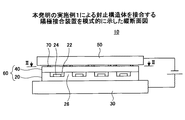
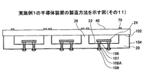
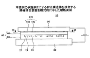
図1は本発明の実施例1による封止構造体を接合する陽極接合装置を模式的に示した縦断面図である。図2は図1中II−II線に沿う横断面図である。図1に示されるように、陽極接合装置10は、シリコン基板20の下面に陽極板30を接触させ、透明なガラス板40の上面に陰極板50を接触させた状態で高電圧を印加することにより、シリコン基板20の上面とガラス板40の下面との間を陽極接合するように構成されている。
FIG. 1 is a longitudinal sectional view schematically showing an anodic bonding apparatus for bonding a sealing structure according to Example 1 of the present invention. FIG. 2 is a cross-sectional view taken along line II-II in FIG. As shown in FIG. 1, the
この場合、陽極接合は、シリコン基板20とガラス板40との間に高電圧を印加し、シリコン基板20とガラス板40の温度を、例えば300〜350℃程度に昇温して行う。尚、ガラス板40は、耐熱性を有するホウ素が加えられたホウ珪酸ガラスが用いられており、陽極接合による熱溶融接合が良好に行なえる。
In this case, the anodic bonding is performed by applying a high voltage between the
シリコン基板20の上面には、複数の凹部22が一定の間隔で配置されており、各凹部22の内部空間には、例えば、光の受光または発光を行う光変換素子24が実装されている。従って、光変換素子24は、凹部22の周囲を囲むように形成された壁部26の内側に収納されている。そして、シリコン基板20とガラス板40との間が陽極接合された封止構造体60は、壁部26の上面がガラス板40に接合されることにより凹部22の上部開口がガラス板40によって気密状態に封止される。
A plurality of
尚、本実施例の封止構造体60は、光変換素子24以外の素子、例えば、前述したMEMS素子などを実装する構成にも適用することが可能である。
Note that the
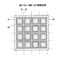
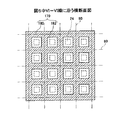
そして、ガラス板40の上面と陰極板50との間には、電圧印加パターン70が形成されている。この電圧印加パターン70は、図2に示されるように、凹部22が対向する非接合領域の周囲を囲む領域に沿う四角枠状(図2中、ハッチングで示す部分)に形成されている。尚、電圧印加パターン70は、凹部22が対向する非接合領域を除く領域に形成されていれば良いので、図2に示すようなパターンに限らず、各電圧印加パターン70を夫々独立させるようなパターンとしても良いし、あるいは、各電圧印加パターン70間を一部または全て接続するようなパターンとすることも可能である。
A
すなわち、この電圧印加パターン70は、壁部26の上面に対応した矩形枠状に形成されており、壁部26の上面とガラス板40との間で効率良く陽極接合を行うことが可能になる。さらに、電圧印加パターン70は、光変換素子24の上方に位置しないように形成されており、光変換素子24が対向する光透過領域を囲むように形成されている。
That is, the
また、電圧印加パターン70は、陰極板50の下面に接触して電圧を印加される陰極パターンとして機能する。そのため、封止構造体60では、電圧印加パターン70に高電圧が印加された際にガラス板40に含まれる不純物(ナトリウム)が電圧印加パターン70に対向する接合領域においてガラス板40の陰極側(接合部分)に析出されるが、凹部22が対向する非接合領域における不純物(ナトリウム)の析出が防止される。
Further, the
これにより、ガラス板40の光透過率が低下することが防止されるため、封止構造体60は、光変換素子24による受光または発光する際の光の透過がガラス板40によって阻害されないように構成されている。また、本実施例の封止構造体60では、シリコン基板20に複数の凹部22が形成されており、複数の凹部22を同時に封止しており、上記陽極接合が終了した後にダイシング工程により図2中一点鎖線で示すスクライブ線80に沿って切断される。
Thereby, since the light transmittance of the
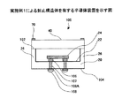
このように陽極接合された封止構造体60より個々の光変換素子24が実装された凹部22毎に切り出された半導体装置100は、図3に示すように構成されている。ここで、半導体装置100の構成について説明する。
The
半導体装置100は、凹部22を有するシリコン基板20と、凹部22に実装された光変換素子24と、ガラス板40とを有し、凹部22を囲む壁部26の上面とガラス板40とを陽極接合して凹部22を封止した構成である。そして、壁部26の上面とガラス板40の下面との接触部分が接合層102となる。
The
また、光変換素子24は、例えばAuよりなるバンプ(Auスタッドバンプ)106上に設置され、光変換素子24は、当該バンプ106を介してシリコン基板20の底面を貫通するように形成されるビアプラグ(貫通配線)107と電気的に接続されている。
The
ビアプラグ107の、光変換素子24が接続される側の反対側には、例えばNi/Auメッキ層よりなる接続層108Aが形成され、さらに当該接続層108Aに半田バンプ108が形成されている。尚、接続層108Aは、半田バンプ108が接合される下面側にAu層が形成されるようにNi層とAu層とが積層されている。
On the opposite side of the via
また、シリコン基板20の表面は、酸化膜(シリコン酸化膜)104が形成され、例えば当該シリコン基板20と、ビアプラグ107との間や、バンプ106との間は絶縁されている。
In addition, an oxide film (silicon oxide film) 104 is formed on the surface of the
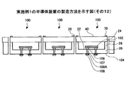
次に、上記の半導体装置100を製造する製造方法の一例について、図4A〜図4Lに基づき、手順を追って説明する。ただし以下の図中、先に説明した部分には同一の参照符号を付し、説明を省略する場合がある。
Next, an example of a manufacturing method for manufacturing the
まず、図4Aに示す工程において、シリコン基板20をエッチングしてパターニングし、光変換素子を設置するための凹部22と、ビアプラグ107を形成するための、シリコン基板20を貫通するビアホール107Aを形成する。
First, in the step shown in FIG. 4A, the
次に、図4Bに示す工程において、凹部22の内壁面やビアホール107Aの内壁面を含むシリコン基板20の表面に、例えば熱CVD(Chemical vaper deposition)法などにより、酸化膜(シリコン酸化膜、または熱酸化膜とよぶ場合もある)104を形成する。
Next, in the step shown in FIG. 4B, an oxide film (silicon oxide film or silicon oxide film) is formed on the surface of the
次に、図4Cに示す工程において、例えばCuのメッキ法(例えばセミアディティブ法)により、ビアホール107Aに、それぞれビアプラグ107を形成する。
Next, in the step shown in FIG. 4C, via
次に、図4Dに示す工程において、例えばメッキ法により、例えばNi/Auよりなる接続層106A,108Aを形成する。この場合、接続層106Aは、ビアプラグ107の凹部22の側に、接続層108Aは、ビアプラグ107の凹部22の反対側に形成される。尚、接続層106A,108Aは、夫々バンプ106,108が接合される接合面がAu層となるようにNi層とAu層とが積層されている。
Next, in the step shown in FIG. 4D, connection layers 106A and 108A made of, for example, Ni / Au are formed by, for example, plating. In this case, the
次に、図4Eに示す工程において、接続層106A上に、それぞれバンプ(Auスタッドバンプ)106を形成する。なお、本図以降では、接続層106Aの図示を省略している。
Next, in the step shown in FIG. 4E, bumps (Au stud bumps) 106 are formed on the
次に、図4Fに示す工程において、凹部22の周囲の壁部26の表面の酸化膜104を、例えばマスクエッチングにより剥離する。本工程によって酸化膜が剥離された部分には後の工程においてガラス板40が接合される。
Next, in the step shown in FIG. 4F, the
次に、図4Gに示す工程において、例えば光変換素子24を凹部22内に設置する。この場合、例えば熱圧着、または超音波接合などを用いて、光変換素子24とバンプ106を電気的に接合し、バンプ106を介して光変換素子24とビアプラグ107が電気的に接続されるように構成する。
Next, in the step shown in FIG. 4G, for example, the
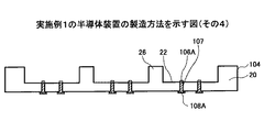
次に、図4Hに示す工程において、ガラス板40の上面(陰極側)に前述した電圧印加パターン70を形成する。電圧印加パターン70の形成法としては、例えば、Cuなどの導電性金属をスパッタ法やCVD法などの薄膜形成技術を用いてガラス板40の上面に積層して形成する。その際、電圧印加パターン70は、図2に示すように、凹部22を囲む壁部26の上面に対向する四角形状となるようにマスクキングを行なって形成される。従って、電圧印加パターン70は、図4Hにおいて、光変換素子24の上面及び凹部22に対向する非接合領域Xの周囲を囲む接合領域Yに沿う形状に形成される。
Next, in the step shown in FIG. 4H, the above-described
また、電圧印加パターン70の厚さは、ガラス板40の上面の平面精度(反りやうねりの大きさ)に応じて設定されており、陰極板50を電圧印加パターン70に接触させた状態でガラス板40の上面と陰極板50とが非接触となる厚さとなるように導電性金属層が積層される。
Further, the thickness of the
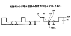
次に、図4Iに示す工程において、ガラス板40をシリコン基板20上に載置する。この工程では、ガラス板40上に形成された電圧印加パターン70がシリコン基板20の壁部26の上面と上下方向で一致(対向)するように相対位置を位置決めして行なわれる。また、この工程において、ガラス板40をシリコン基板20上に載置する際、例えば、粘着性を有する仮止めテープ等を用いてガラス板40とシリコン基板20との相対位置がずれないように接着しても良い。
Next, in the step shown in FIG. 4I, the
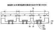
次に、図4Jに示す工程において、シリコン基板20を陽極接合装置10の陽極板30に載置し、陽極接合装置10の陰極板50をガラス板40の上面に形成された電圧印加パターン70に接触させた状態で陽極板30と陰極板50との間に高電圧を印加する。このとき、陰極板50は、電圧印加パターン70に接触することでガラス板40の上面から微小隙間を介して離間した状態になる。
4J, the
また、陽極板30の上面には、シリコン基板20の下面に突出する接続層108Aと接触しないように凹部32が形成されている。そのため、陽極板30は、光変換素子24の下面が対向する領域に凹部32が形成され、凹部32を囲む上面がシリコン基板20の下面に接触している。
Further, a
ガラス板40に対する電圧印加は、電圧印加パターン70を介して行なわれるため、ガラス板40は電圧印加パターン70に対向する接合領域Yが加熱された状態になり、シリコン基板20の壁部26上面に接合される。よって、凹部22及び光変換素子24が対向する非接合領域Xに不純物(ナトリウム)が析出することが防止される。これにより、ガラス板40は、光変換素子24が対向する非接合領域Xの光透過率の低下が発生せず、光変換素子24の受光または発光を阻害しないように接合される。
Since the voltage application to the
上記の陽極接合が行われると、シリコン基板20を構成するSiと、ガラス板40中の酸素とが結合し、接合力が良好で安定した接合が行われる。また、陽極接合では、樹脂材料を用いた接合と異なり、光変換素子24が封止される凹部22の内部空間を汚染するようなガス、不純物などが殆ど発生することがない。
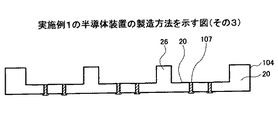
When the above anodic bonding is performed, Si constituting the
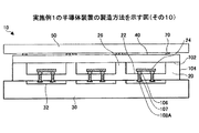
次に、図4Kに示す工程において、接続層108Aにそれぞれ半田バンプ108を形成する。また、この図4Kに示す工程において、エッチングによりガラス板40に形成された電圧印加パターン70を除去しても良い。さらに、この工程において、上記半田バンプ108を設けずに接続層108A自体を外部接続端子として用いても良い。
Next, in the step shown in FIG. 4K, solder bumps 108 are formed on the
次に、図4Lに示す工程において、陽極接合により一体化された封止構造体60をスクライブ線80に沿ってダイシングにより切断し、個片化することで、先に説明した半導体装置100を得ることができる。この切断工程により個片化された半導体装置100は、ガラス板40の上面に電圧印加パターン70が残った状態であるが、光変換素子24の発光及び受光を妨げない位置にあるので、そのまま残しておいても良い。あるいは、半導体装置100をマザーボード等に実装する際に電圧印加パターン70を陽極接合されていることを識別するための識別マークとして活用することも可能である。
Next, in the step shown in FIG. 4L, the sealing
また、電圧印加パターン70の幅を狭く形成することで、スクライブ線80に沿って電圧印加パターン70を形成することが可能になる。この場合、ダイシング工程で切断する際に電圧印加パターン70も同時に削除することが可能になり、電圧印加パターン70を剥離させる必要がある場合には、剥離工程を不要にすることができる。
In addition, the
図5は本発明の実施例2による封止構造体を接合する陽極接合装置を模式的に示した縦断面図である。図6は図5中VI−VI線に沿う横断面図である。尚、図5及び図6において、上記実施例1と同一部分には同一符号を付してその説明を省略する。 FIG. 5 is a longitudinal sectional view schematically showing an anodic bonding apparatus for bonding a sealing structure according to Example 2 of the present invention. FIG. 6 is a cross-sectional view taken along line VI-VI in FIG. 5 and 6, the same parts as those in the first embodiment are denoted by the same reference numerals, and the description thereof is omitted.
図5に示されるように、ガラス板40の上面と陰極板50との間には、電圧印加パターン170が形成されている。この電圧印加パターン170は、図6に示されるように、凹部22が対向する非接合領域の周囲を囲む領域に沿う格子状(図6中、ハッチングで示す部分)に形成されている。
As shown in FIG. 5, a
この電圧印加パターン170の形成方法としては、まず、Cuなどの導電性金属をメッキ法を用いてガラス板40の上面(同一平面上)全体に積層させて均一な厚さを有する導電性金属層180を形成する。次に、導電性金属層180のうち凹部22が対向する非接合領域をマスクエッチングにより除去して上下方向に貫通する貫通孔182を形成する。
As a method for forming the
これで、貫通孔182を有する導電性金属層180によって形成された電圧印加パターン170を得られる。
Thus, the
電圧印加パターン170は、光変換素子24の上方に位置しないように形成されており、光変換素子24が対向する光透過領域を囲むように形成されている。また、電圧印加パターン170は、陰極板50の下面に接触して電圧を印加される陰極パターンとして機能する。そのため、電圧印加パターン170に高電圧が印加された際にガラス板40に含まれる不純物(ナトリウム)が電圧印加パターン170に対向する接合領域においてガラス板40の陰極側(接合部分)に析出されるが、凹部22が対向する非接合領域(光透過領域)における不純物(ナトリウム)の析出が防止される。
The
図7は本発明の実施例3による封止構造体を接合する陽極接合装置を模式的に示した縦断面図である。図8は図7中VIII−VIII線に沿う横断面図である。尚、図7及び図8において、上記実施例1と同一部分には同一符号を付してその説明を省略する。 FIG. 7 is a longitudinal sectional view schematically showing an anodic bonding apparatus for bonding a sealing structure according to Example 3 of the present invention. FIG. 8 is a transverse sectional view taken along line VIII-VIII in FIG. 7 and 8, the same parts as those in the first embodiment are denoted by the same reference numerals, and the description thereof is omitted.
図7に示されるように、ガラス板40の上面と陰極板50との間には、電圧印加パターン270が形成されている。この電圧印加パターン270は、図8に示されるように、陰極板50の下面に設けられており、凹部22が対向する非接合領域(光透過領域)の周囲を囲む領域に沿う格子状(図8中、ハッチングで示す部分)に形成されている。
As shown in FIG. 7, a
この電圧印加パターン270は、陰極板50の表面の非接合領域に対向する領域に非接触部としての逃げ部52を設けることにより形成することができる。従って、逃げ部52が凹部22に対向する位置に配置されることで、陰極板50の下面には、非接合領域(光透過領域)の周囲を囲む接合領域に沿う電圧印加パターン270が形成される。
The
そして、陰極板50の下面に形成された電圧印加パターン270をガラス板40の上面に接触させた状態で、電圧印加パターン270に高電圧が印加されると、ガラス板40に含まれる不純物(ナトリウム)が電圧印加パターン270に対向する接合領域においてガラス板40の陰極側(接合部分)に析出されるが、凹部22が対向する非接合領域(光透過領域)における不純物(ナトリウム)の析出が防止される。
Then, when a high voltage is applied to the
本実施例では、陰極板50の下面に電圧印加パターン270が一体形成されているので、前述した実施例のように電圧印加パターンをガラス板40に形成する工程を省くことができると共に、完成した半導体装置にも電圧印加パターンが残らないので、電圧印加パターンを除去する工程も省くことができる。
In this embodiment, since the
以上、本発明を好ましい実施例について説明したが、本発明は上記の特定の実施例に限定されるものではなく、特許請求の範囲に記載した要旨内において様々な変形・変更が可能である。 Although the present invention has been described with reference to the preferred embodiments, the present invention is not limited to the specific embodiments described above, and various modifications and changes can be made within the scope described in the claims.
図9は実施例4による封止構造体を有する半導体装置を示す図である。尚、図9において、上記図3と同一部分には、同一符号を付してその説明を省略する。図9に示されるように、半導体装置200は、平板状に形成されたシリコン基板20と、下面側に凹部22が形成されたガラス板40と、シリコン基板20上に実装された状態でガラス板40の凹部22内に収納される光変換素子24と、を有し、ガラス板40に設けられた凹部22を囲む壁部26の下面と、シリコン基板20の上面とを陽極接合して凹部22を気密状態に封止した構成である。そして、ガラス板40に設けられた壁部26の下面とシリコン基板20の上面との接触部分が接合層102となる。
FIG. 9 is a diagram illustrating a semiconductor device having a sealing structure according to the fourth embodiment. In FIG. 9, the same parts as those in FIG. As shown in FIG. 9, the
この実施例4の場合も上記実施例と同様に、陽極接合装置10(図1、図5、図7を参照)は、シリコン基板20の下面に陽極板30を接触させ、透明なガラス板40の上面に陰極板50を接触させた状態で高電圧を印加することにより、シリコン基板20の上面とガラス板40の下面との間を陽極接合する。
In the case of Example 4, as in the above example, the anodic bonding apparatus 10 (see FIGS. 1, 5, and 7) brings the
従って、接合層102は、前述した電圧印加パターン70,170,270を介して陽極接合装置10により陽極接合される。本実施例では、ガラス板40の下面に凹部22が形成されているので、凹部22を囲む壁部26もガラスによって形成されている。そのため、陽極接合により封止された凹部22内に実装された光変換素子24は、側面を囲む壁部26を透過する光を発光または受光することができる。
Therefore, the
このように、前述した実施例1〜3では、シリコン基板20に凹部22を形成し、この凹部22に光変換素子24を実装した構成を例に挙げたが、本実施例では、シリコン基板20を平板状に形成し、ガラス板40の下面に凹部22を形成し、シリコン基板20上に実装された光変換素子24をガラス板40の凹部22によって封止する構成とされた封止構造体よりなる半導体装置200にも本発明の製造方法を適用することができる。
As described above, in the first to third embodiments, the configuration in which the
尚、上記実施例では、シリコン基板20の凹部22に光変換素子24を実装してガラス板40により封止する構成の封止構造体及び半導体装置を例に挙げて説明したが、これに限らず、陽極接合を用いて接合する封止構造であれば、上記実施例のような構成のものでなくても本発明を適用できるのは勿論である。
In the above-described embodiment, the sealing structure and the semiconductor device having the configuration in which the
10 陽極接合装置
20 シリコン基板
22 凹部
24 光変換素子
26 壁部
30 陽極板
40 ガラス板
50 陰極板
60 封止構造体
70,170,270 電圧印加パターン
100,200 半導体装置
102 接合層
180 導電性金属層
182 貫通孔
DESCRIPTION OF
Claims (10)
前記ガラス板と前記陰極板との間に、前記凹部が対向する非接合領域の周囲を囲む接合領域に沿う電圧印加パターンを形成し、前記電圧印加パターンに高電圧を印加して前記凹部を囲む壁部を前記ガラス板または前記シリコン基板に陽極接合したことを特徴とする封止構造体。 A recess is provided in either the silicon substrate or the glass plate bonded to the silicon substrate, the anode plate is brought into contact with the silicon substrate, the cathode plate is brought into contact with the glass plate, and the silicon substrate and the glass plate are anoded. A sealing structure that seals the recess by bonding,
A voltage application pattern is formed between the glass plate and the cathode plate along a bonding region surrounding the periphery of the non-bonding region facing the concave portion, and a high voltage is applied to the voltage application pattern to surround the concave portion. A sealing structure characterized in that a wall portion is anodically bonded to the glass plate or the silicon substrate.
前記ガラス板と前記陰極板との間に、前記凹部が対向する非接合領域の周囲を囲む接合領域に沿う電圧印加パターンを形成する工程と、
前記シリコン基板にガラス板を載置して前記凹部を閉塞する工程と、
前記電圧印加パターンに高電圧を印加して前記凹部を囲む壁部を前記ガラス板または前記シリコン基板に陽極接合する工程と、
を有することを特徴とする封止構造体の製造方法。 A recess is provided in either the silicon substrate or the glass plate bonded to the silicon substrate, the anode plate is brought into contact with the silicon substrate, the cathode plate is brought into contact with the glass plate, and the silicon substrate and the glass plate are anoded. A method for producing a sealing structure that seals the recess by bonding,
Forming a voltage application pattern along a bonding region surrounding the non-bonding region facing the concave portion between the glass plate and the cathode plate;
Placing a glass plate on the silicon substrate and closing the recess;
Applying a high voltage to the voltage application pattern and anodically bonding the wall surrounding the recess to the glass plate or the silicon substrate;
The manufacturing method of the sealing structure characterized by having.
前記ガラス板と前記陰極板との間に、前記素子が対向する光透過領域の周囲を囲む領域に沿う電圧印加パターンを形成し、前記電圧印加パターンに高電圧を印加して前記凹部を囲む壁部を前記ガラス板または前記シリコン基板に陽極接合したことを特徴とする半導体装置。 The silicon substrate or a glass plate bonded to the silicon substrate is provided with a recess, an element is mounted in the recess, the anode plate is contacted with the silicon substrate, and the cathode plate is contacted with the glass plate. A semiconductor device that seals the recess by anodically bonding a silicon substrate and the glass plate,
A wall is formed between the glass plate and the cathode plate to form a voltage application pattern along a region surrounding the periphery of the light transmission region facing the device, and a high voltage is applied to the voltage application pattern to surround the recess. A semiconductor device characterized in that a part is anodically bonded to the glass plate or the silicon substrate.
前記凹部内に素子を実装する工程と、
前記ガラス板と前記陰極板との間に、前記素子が対向する光透過領域の周囲を囲む領域に沿う電圧印加パターンを形成する工程と、
前記シリコン基板にガラス板を載置して前記凹部を閉塞する工程と、
前記電圧印加パターンに高電圧を印加して前記凹部を囲む壁部を前記ガラス板または前記シリコン基板に陽極接合する工程と、
を有することを特徴とする半導体装置の製造方法。 A recess is provided in either the silicon substrate or the glass plate bonded to the silicon substrate, the anode plate is brought into contact with the silicon substrate, the cathode plate is brought into contact with the glass plate, and the silicon substrate and the glass plate are anoded. A method of manufacturing a semiconductor device having a sealing structure that seals the recess by bonding,
Mounting an element in the recess;
Forming a voltage application pattern between the glass plate and the cathode plate along a region surrounding the periphery of the light transmission region facing the element;
Placing a glass plate on the silicon substrate and closing the recess;
Applying a high voltage to the voltage application pattern and anodically bonding the wall surrounding the recess to the glass plate or the silicon substrate;
A method for manufacturing a semiconductor device, comprising:
Priority Applications (4)
| Application Number | Priority Date | Filing Date | Title |
|---|---|---|---|
| JP2006019286A JP2007201260A (en) | 2006-01-27 | 2006-01-27 | Sealing structure, method of manufacturing sealing structure, semiconductor device, and method of manufacturing semiconductor device |
| US11/624,440 US7834438B2 (en) | 2006-01-27 | 2007-01-18 | Sealed structure and method of fabricating sealed structure and semiconductor device and method of fabricating semiconductor device |
| TW096102264A TW200733313A (en) | 2006-01-27 | 2007-01-22 | Sealed structure and method of fabricating sealed structure and semiconductor device and method of fabricating semiconductor device |
| EP07001893A EP1813571A2 (en) | 2006-01-27 | 2007-01-29 | Sealed structure and method of fabricating the sealed structure |
Applications Claiming Priority (1)
| Application Number | Priority Date | Filing Date | Title |
|---|---|---|---|
| JP2006019286A JP2007201260A (en) | 2006-01-27 | 2006-01-27 | Sealing structure, method of manufacturing sealing structure, semiconductor device, and method of manufacturing semiconductor device |
Publications (1)
| Publication Number | Publication Date |
|---|---|
| JP2007201260A true JP2007201260A (en) | 2007-08-09 |
Family
ID=38051857
Family Applications (1)
| Application Number | Title | Priority Date | Filing Date |
|---|---|---|---|
| JP2006019286A Pending JP2007201260A (en) | 2006-01-27 | 2006-01-27 | Sealing structure, method of manufacturing sealing structure, semiconductor device, and method of manufacturing semiconductor device |
Country Status (4)
| Country | Link |
|---|---|
| US (1) | US7834438B2 (en) |
| EP (1) | EP1813571A2 (en) |
| JP (1) | JP2007201260A (en) |
| TW (1) | TW200733313A (en) |
Cited By (4)
| Publication number | Priority date | Publication date | Assignee | Title |
|---|---|---|---|---|
| JP2011041069A (en) * | 2009-08-12 | 2011-02-24 | Seiko Instruments Inc | Method for manufacturing package, method for manufacturing piezoelectric vibrator, piezoelectric vibrator, oscillator, electronic equipment, and radio-controlled timepiece |
| JP2011049324A (en) * | 2009-08-26 | 2011-03-10 | Seiko Instruments Inc | Anode boding method and method of manufacturing piezoelectric vibrator |
| JP2011049663A (en) * | 2009-08-25 | 2011-03-10 | Seiko Instruments Inc | Package manufacturing method, piezoelectric vibrator manufacturing method, oscillator, electronic equipment, and radio wave clock |
| JP2011143479A (en) * | 2010-01-12 | 2011-07-28 | Dainippon Printing Co Ltd | Method for manufacturing mems device and mems device |
Families Citing this family (10)
| Publication number | Priority date | Publication date | Assignee | Title |
|---|---|---|---|---|
| TW200737506A (en) * | 2006-03-07 | 2007-10-01 | Sanyo Electric Co | Semiconductor device and manufacturing method of the same |
| TWI367557B (en) * | 2006-08-11 | 2012-07-01 | Sanyo Electric Co | Semiconductor device and manufaturing method thereof |
| JP5010247B2 (en) * | 2006-11-20 | 2012-08-29 | オンセミコンダクター・トレーディング・リミテッド | Semiconductor device and manufacturing method thereof |
| US20090181500A1 (en) * | 2008-01-15 | 2009-07-16 | Jochen Kuhmann | Fabrication of Compact Semiconductor Packages |
| US8390083B2 (en) | 2009-09-04 | 2013-03-05 | Analog Devices, Inc. | System with recessed sensing or processing elements |
| WO2012051340A1 (en) | 2010-10-12 | 2012-04-19 | Analog Devices, Inc. | Microphone package with embedded asic |
| CN103130180B (en) * | 2011-12-02 | 2015-10-28 | 中国科学院微电子研究所 | A kind of wafer scale anode linkage method |
| US9847462B2 (en) | 2013-10-29 | 2017-12-19 | Point Engineering Co., Ltd. | Array substrate for mounting chip and method for manufacturing the same |
| US9666558B2 (en) | 2015-06-29 | 2017-05-30 | Point Engineering Co., Ltd. | Substrate for mounting a chip and chip package using the substrate |
| DE102016116499B4 (en) * | 2016-09-02 | 2022-06-15 | Infineon Technologies Ag | Process for forming semiconductor devices and semiconductor devices |
Citations (4)
| Publication number | Priority date | Publication date | Assignee | Title |
|---|---|---|---|---|
| JP2000211951A (en) * | 1999-01-22 | 2000-08-02 | Canon Inc | Method for vacuum sealing using anodic junction and vacuum device |
| JP2001196486A (en) * | 2000-01-07 | 2001-07-19 | Murata Mfg Co Ltd | Reduced-pressure package structure and manufacturing method thereof |
| JP2005187321A (en) * | 2003-12-02 | 2005-07-14 | Bondotekku:Kk | Bonding method, device produced by this method, and bonding device |
| JP2006100614A (en) * | 2004-09-30 | 2006-04-13 | Hitachi Ltd | Electronic device using anode junction structure |
Family Cites Families (4)
| Publication number | Priority date | Publication date | Assignee | Title |
|---|---|---|---|---|
| US5766053A (en) * | 1995-02-10 | 1998-06-16 | Micron Technology, Inc. | Internal plate flat-panel field emission display |
| JP3347648B2 (en) * | 1997-08-19 | 2002-11-20 | 富士通株式会社 | Display device |
| JP2004241130A (en) * | 2003-02-03 | 2004-08-26 | Seiko Epson Corp | Luminescent display panel and its manufacturing method |
| JP3975194B2 (en) | 2003-12-02 | 2007-09-12 | 株式会社フジクラ | Package manufacturing method |
-
2006
- 2006-01-27 JP JP2006019286A patent/JP2007201260A/en active Pending
-
2007
- 2007-01-18 US US11/624,440 patent/US7834438B2/en active Active
- 2007-01-22 TW TW096102264A patent/TW200733313A/en unknown
- 2007-01-29 EP EP07001893A patent/EP1813571A2/en not_active Withdrawn
Patent Citations (4)
| Publication number | Priority date | Publication date | Assignee | Title |
|---|---|---|---|---|
| JP2000211951A (en) * | 1999-01-22 | 2000-08-02 | Canon Inc | Method for vacuum sealing using anodic junction and vacuum device |
| JP2001196486A (en) * | 2000-01-07 | 2001-07-19 | Murata Mfg Co Ltd | Reduced-pressure package structure and manufacturing method thereof |
| JP2005187321A (en) * | 2003-12-02 | 2005-07-14 | Bondotekku:Kk | Bonding method, device produced by this method, and bonding device |
| JP2006100614A (en) * | 2004-09-30 | 2006-04-13 | Hitachi Ltd | Electronic device using anode junction structure |
Cited By (6)
| Publication number | Priority date | Publication date | Assignee | Title |
|---|---|---|---|---|
| JP2011041069A (en) * | 2009-08-12 | 2011-02-24 | Seiko Instruments Inc | Method for manufacturing package, method for manufacturing piezoelectric vibrator, piezoelectric vibrator, oscillator, electronic equipment, and radio-controlled timepiece |
| JP2011049663A (en) * | 2009-08-25 | 2011-03-10 | Seiko Instruments Inc | Package manufacturing method, piezoelectric vibrator manufacturing method, oscillator, electronic equipment, and radio wave clock |
| CN101997502A (en) * | 2009-08-25 | 2011-03-30 | 精工电子有限公司 | Method for manufacturing package, method of manufacturing piezoelectric vibrator, oscillator, electronic device, and radio-controlled timepiece |
| CN101997502B (en) * | 2009-08-25 | 2015-05-20 | 精工电子有限公司 | Method for manufacturing package, method of manufacturing piezoelectric vibrator, oscillator, electronic device, and radio-controlled timepiece |
| JP2011049324A (en) * | 2009-08-26 | 2011-03-10 | Seiko Instruments Inc | Anode boding method and method of manufacturing piezoelectric vibrator |
| JP2011143479A (en) * | 2010-01-12 | 2011-07-28 | Dainippon Printing Co Ltd | Method for manufacturing mems device and mems device |
Also Published As
| Publication number | Publication date |
|---|---|
| EP1813571A2 (en) | 2007-08-01 |
| TW200733313A (en) | 2007-09-01 |
| US20070177360A1 (en) | 2007-08-02 |
| US7834438B2 (en) | 2010-11-16 |
Similar Documents
| Publication | Publication Date | Title |
|---|---|---|
| JP2007201260A (en) | Sealing structure, method of manufacturing sealing structure, semiconductor device, and method of manufacturing semiconductor device | |
| JP5154819B2 (en) | Substrate and manufacturing method thereof | |
| KR100907514B1 (en) | Sensor device, sensor system and method of manufacturing the same | |
| JP5028486B2 (en) | Manufacturing method of semiconductor device | |
| TW200817278A (en) | Mems device and method of fabricating the same | |
| JP6247006B2 (en) | Electronic device, oscillator, and method of manufacturing electronic device | |
| US7154053B2 (en) | Optoelectronic package with wire-protection lid | |
| JP2011131309A (en) | Method for manufacturing semiconductor package | |
| JP2007027279A (en) | Semiconductor device and manufacturing method thereof | |
| JP2010230655A (en) | Sensor device and manufacturing method thereof | |
| JP2012169564A (en) | Wafer level package, chip size package device, and method of manufacturing wafer level package | |
| EP1898462B1 (en) | Semiconductor apparatus | |
| JP2005129888A (en) | Sensor device and sensor system, and manufacturing method therefor | |
| JP2007173915A (en) | Piezoelectric device unit and method of manufacturing same | |
| CN102311093B (en) | Method for forming the chip package | |
| JP5248179B2 (en) | Manufacturing method of electronic device | |
| JP2010081127A (en) | Crystal oscillator and method of manufacturing same | |
| JP2006186357A (en) | Sensor device and its manufacturing method | |
| JP2014165341A (en) | Electronic device | |
| JP5769482B2 (en) | Manufacturing method of glass sealed package and optical device | |
| JP2008221456A (en) | Dicing technology relating to flip chip usp wafer | |
| JP2005039078A (en) | Wafer substrate for sheet substrate structure formation, method for manufacturing the same, and method for manufacturing mems element | |
| JP4663450B2 (en) | Method for manufacturing photoelectric integrated circuit device | |
| JP5955024B2 (en) | MEMS module and manufacturing method thereof | |
| JP7265728B2 (en) | Mounting substrate and mounting substrate manufacturing method |
Legal Events
| Date | Code | Title | Description |
|---|---|---|---|
| A621 | Written request for application examination |
Free format text: JAPANESE INTERMEDIATE CODE: A621 Effective date: 20081017 |
|
| A977 | Report on retrieval |
Free format text: JAPANESE INTERMEDIATE CODE: A971007 Effective date: 20090623 |
|
| A131 | Notification of reasons for refusal |
Free format text: JAPANESE INTERMEDIATE CODE: A131 Effective date: 20110104 |
|
| A02 | Decision of refusal |
Free format text: JAPANESE INTERMEDIATE CODE: A02 Effective date: 20110426 |