EP2342591B1 - Variable transmission composite interference filter - Google Patents
Variable transmission composite interference filter Download PDFInfo
- Publication number
- EP2342591B1 EP2342591B1 EP09744281.8A EP09744281A EP2342591B1 EP 2342591 B1 EP2342591 B1 EP 2342591B1 EP 09744281 A EP09744281 A EP 09744281A EP 2342591 B1 EP2342591 B1 EP 2342591B1
- Authority
- EP
- European Patent Office
- Prior art keywords
- interference filter
- band pass
- band
- composite
- angle
- Prior art date
- Legal status (The legal status is an assumption and is not a legal conclusion. Google has not performed a legal analysis and makes no representation as to the accuracy of the status listed.)
- Not-in-force
Links
- 239000002131 composite material Substances 0.000 title claims description 37
- 230000005540 biological transmission Effects 0.000 title claims description 33
- 229920006254 polymer film Polymers 0.000 claims description 36
- 125000006850 spacer group Chemical group 0.000 claims description 28
- -1 poly(ethylene terephthalate) Polymers 0.000 claims description 16
- 239000000463 material Substances 0.000 claims description 15
- GWEVSGVZZGPLCZ-UHFFFAOYSA-N Titan oxide Chemical compound O=[Ti]=O GWEVSGVZZGPLCZ-UHFFFAOYSA-N 0.000 claims description 8
- 238000001429 visible spectrum Methods 0.000 claims description 7
- 238000000034 method Methods 0.000 claims description 6
- 229920000139 polyethylene terephthalate Polymers 0.000 claims description 6
- 239000005020 polyethylene terephthalate Substances 0.000 claims description 6
- 230000009467 reduction Effects 0.000 claims description 5
- 239000012939 laminating adhesive Substances 0.000 claims description 4
- 229910001635 magnesium fluoride Inorganic materials 0.000 claims description 4
- VYPSYNLAJGMNEJ-UHFFFAOYSA-N silicon dioxide Inorganic materials O=[Si]=O VYPSYNLAJGMNEJ-UHFFFAOYSA-N 0.000 claims description 4
- BQCADISMDOOEFD-UHFFFAOYSA-N Silver Chemical compound [Ag] BQCADISMDOOEFD-UHFFFAOYSA-N 0.000 claims description 3
- 239000000853 adhesive Substances 0.000 claims description 3
- 230000001070 adhesive effect Effects 0.000 claims description 3
- ZKATWMILCYLAPD-UHFFFAOYSA-N niobium pentoxide Inorganic materials O=[Nb](=O)O[Nb](=O)=O ZKATWMILCYLAPD-UHFFFAOYSA-N 0.000 claims description 3
- 229910052709 silver Inorganic materials 0.000 claims description 3
- 239000004332 silver Substances 0.000 claims description 3
- RYGMFSIKBFXOCR-UHFFFAOYSA-N Copper Chemical compound [Cu] RYGMFSIKBFXOCR-UHFFFAOYSA-N 0.000 claims description 2
- 229910052782 aluminium Inorganic materials 0.000 claims description 2
- XAGFODPZIPBFFR-UHFFFAOYSA-N aluminium Chemical compound [Al] XAGFODPZIPBFFR-UHFFFAOYSA-N 0.000 claims description 2
- 229910052681 coesite Inorganic materials 0.000 claims description 2
- 229910052802 copper Inorganic materials 0.000 claims description 2
- 239000010949 copper Substances 0.000 claims description 2
- 229910052906 cristobalite Inorganic materials 0.000 claims description 2
- PCHJSUWPFVWCPO-UHFFFAOYSA-N gold Chemical compound [Au] PCHJSUWPFVWCPO-UHFFFAOYSA-N 0.000 claims description 2
- 229910052737 gold Inorganic materials 0.000 claims description 2
- 239000010931 gold Substances 0.000 claims description 2
- 229910052682 stishovite Inorganic materials 0.000 claims description 2
- 238000000411 transmission spectrum Methods 0.000 claims description 2
- 229910052905 tridymite Inorganic materials 0.000 claims description 2
- 230000005670 electromagnetic radiation Effects 0.000 claims 2
- 239000003570 air Substances 0.000 claims 1
- 239000010410 layer Substances 0.000 description 64
- 239000000758 substrate Substances 0.000 description 14
- 239000010408 film Substances 0.000 description 13
- 230000000694 effects Effects 0.000 description 7
- 239000003989 dielectric material Substances 0.000 description 6
- 238000001914 filtration Methods 0.000 description 6
- 239000011521 glass Substances 0.000 description 6
- 230000003287 optical effect Effects 0.000 description 6
- 239000004033 plastic Substances 0.000 description 4
- 229920003023 plastic Polymers 0.000 description 4
- 238000001228 spectrum Methods 0.000 description 4
- 239000010409 thin film Substances 0.000 description 4
- 229910021417 amorphous silicon Inorganic materials 0.000 description 3
- 230000009977 dual effect Effects 0.000 description 3
- 229910052751 metal Inorganic materials 0.000 description 3
- 239000002184 metal Substances 0.000 description 3
- 239000002210 silicon-based material Substances 0.000 description 3
- 238000010521 absorption reaction Methods 0.000 description 2
- 230000015572 biosynthetic process Effects 0.000 description 2
- 230000008859 change Effects 0.000 description 2
- 229920002037 poly(vinyl butyral) polymer Polymers 0.000 description 2
- 229920000515 polycarbonate Polymers 0.000 description 2
- 239000004417 polycarbonate Substances 0.000 description 2
- 229920000728 polyester Polymers 0.000 description 2
- 229920002635 polyurethane Polymers 0.000 description 2
- 239000004814 polyurethane Substances 0.000 description 2
- 239000011241 protective layer Substances 0.000 description 2
- 230000005855 radiation Effects 0.000 description 2
- 238000004544 sputter deposition Methods 0.000 description 2
- 229920001169 thermoplastic Polymers 0.000 description 2
- 239000004416 thermosoftening plastic Substances 0.000 description 2
- 229910001316 Ag alloy Inorganic materials 0.000 description 1
- 229920002284 Cellulose triacetate Polymers 0.000 description 1
- 239000004743 Polypropylene Substances 0.000 description 1
- 229910004205 SiNX Inorganic materials 0.000 description 1
- BZHJMEDXRYGGRV-UHFFFAOYSA-N Vinyl chloride Chemical compound ClC=C BZHJMEDXRYGGRV-UHFFFAOYSA-N 0.000 description 1
- 239000005083 Zinc sulfide Substances 0.000 description 1
- 229920006397 acrylic thermoplastic Polymers 0.000 description 1
- 229910045601 alloy Inorganic materials 0.000 description 1
- 239000000956 alloy Substances 0.000 description 1
- 238000003491 array Methods 0.000 description 1
- 230000004888 barrier function Effects 0.000 description 1
- 229920002301 cellulose acetate Polymers 0.000 description 1
- 238000005229 chemical vapour deposition Methods 0.000 description 1
- 238000004891 communication Methods 0.000 description 1
- 229920001577 copolymer Polymers 0.000 description 1
- 230000008878 coupling Effects 0.000 description 1
- 238000010168 coupling process Methods 0.000 description 1
- 238000005859 coupling reaction Methods 0.000 description 1
- 238000000151 deposition Methods 0.000 description 1
- 230000008030 elimination Effects 0.000 description 1
- 238000003379 elimination reaction Methods 0.000 description 1
- 230000008020 evaporation Effects 0.000 description 1
- 238000001704 evaporation Methods 0.000 description 1
- 238000009499 grossing Methods 0.000 description 1
- ORUIBWPALBXDOA-UHFFFAOYSA-L magnesium fluoride Chemical compound [F-].[F-].[Mg+2] ORUIBWPALBXDOA-UHFFFAOYSA-L 0.000 description 1
- 239000000203 mixture Substances 0.000 description 1
- 230000004048 modification Effects 0.000 description 1
- 238000012986 modification Methods 0.000 description 1
- 229920001778 nylon Polymers 0.000 description 1
- 239000012788 optical film Substances 0.000 description 1
- 238000005240 physical vapour deposition Methods 0.000 description 1
- 229920003229 poly(methyl methacrylate) Polymers 0.000 description 1
- 229920006267 polyester film Polymers 0.000 description 1
- 229920000642 polymer Polymers 0.000 description 1
- 229920000098 polyolefin Polymers 0.000 description 1
- 229920001155 polypropylene Polymers 0.000 description 1
- 229920001296 polysiloxane Polymers 0.000 description 1
- 230000008569 process Effects 0.000 description 1
- 239000000377 silicon dioxide Substances 0.000 description 1
- 235000012239 silicon dioxide Nutrition 0.000 description 1
- 229910052814 silicon oxide Inorganic materials 0.000 description 1
- 239000002356 single layer Substances 0.000 description 1
- 239000000126 substance Substances 0.000 description 1
- ISXSCDLOGDJUNJ-UHFFFAOYSA-N tert-butyl prop-2-enoate Chemical compound CC(C)(C)OC(=O)C=C ISXSCDLOGDJUNJ-UHFFFAOYSA-N 0.000 description 1
- 238000000427 thin-film deposition Methods 0.000 description 1
- 239000004408 titanium dioxide Substances 0.000 description 1
- 229920002554 vinyl polymer Polymers 0.000 description 1
- 230000000007 visual effect Effects 0.000 description 1
- 229910052984 zinc sulfide Inorganic materials 0.000 description 1
- DRDVZXDWVBGGMH-UHFFFAOYSA-N zinc;sulfide Chemical compound [S-2].[Zn+2] DRDVZXDWVBGGMH-UHFFFAOYSA-N 0.000 description 1
Images
Classifications
-
- G—PHYSICS
- G02—OPTICS
- G02B—OPTICAL ELEMENTS, SYSTEMS OR APPARATUS
- G02B5/00—Optical elements other than lenses
- G02B5/20—Filters
- G02B5/28—Interference filters
-
- G—PHYSICS
- G02—OPTICS
- G02B—OPTICAL ELEMENTS, SYSTEMS OR APPARATUS
- G02B5/00—Optical elements other than lenses
- G02B5/20—Filters
- G02B5/28—Interference filters
- G02B5/285—Interference filters comprising deposited thin solid films
- G02B5/288—Interference filters comprising deposited thin solid films comprising at least one thin film resonant cavity, e.g. in bandpass filters
Definitions
- the present invention is in the field of light filters in general, and, in particular, the present invention is in the field of band pass interference filters used to selectively transmit desired wavelengths of visible light.
- a source of white light or light comprising components from wavelengths throughout the visible spectrum is filtered so as to transmit only the desired wavelengths.
- absorption filters and interference filters are in common use.
- One type of interference filter utilizes a dielectric layer disposed between two very thin layers of a reflective material.
- the resulting filter transmits light within a band of the visible spectrum.
- the wavelength band of the transmitted light is not constant at all angles of incidence, however.
- the transmitted band will shift as the angle is changed.
- the apparent color of transmitted light will therefore change as the viewing angle of an observer is changed.
- the wavelength of light that is transmitted and the magnitude of the band shift are directly related to the thickness of the dielectric layer and the index of refraction of the dielectric material.
- band pass interference filters can be manufactured to transmit light in a wide variety of bands along the visible light spectrum.
- US-A-5 502 595 discloses a color filter comprising a transparent substrate and two or more multilayer films of amorphous silicon materials deposited on said substrate, each film being different, each layer of said two or more multi-layer films having a thickness less than the wavelength of the visible light and at least three layers of said two or more multi-layer films of amorphous silicon materials in an alternate arrangement wherein the amorphous silicon materials are selected from a-SiOx and a-SiNx.
- US 2006/007547 discloses a multi-bandpass filter comprising a thin film superimposed layer portion by mirror layers, cavity layers, etc., provided on a substrate with two kinds of dielectrics having different refractive indices, the optical film thickness thereof being a quarter of a reference wavelength as one unit, so as to form a plurality of Fabry-Perrot interferometer structures.
- US 6 031 653 discloses interference filters and filter arrays based on thin-metal film interference filters having at least one dielectric layer formed between two thin-metal films to form a Fabry-Perot cavity.
- US 2005/018301 discloses in an optical element, a first mirror stack layer formed on a substrate, and a spacer layer made of a paraelectric material having a secondary electrooptic effect is formed thereon through a first conductive thin film.
- a second mirror stack layer is formed thereon through a second conductive thin film, and a coupling layer is formed thereon.
- interference filters are provided that incorporate two band pass interference filters into a single composite interference filter.
- the two filters each have at least one band pass curve that is centered at the same wavelength for light that is incident at a given angle to the filter surface.
- the band pass curve shifts of the filter components are dissimilar, which results in a decrease of transmitted light as the angle of incidence diverges from the given angle.
- the present invention provides interference filters that can be used in a wide variety of applications, including, for example, as a privacy barrier that restricts complete viewing of an area through a window onto which a filter has been affixed.
- Interference filters of the present invention are composite filters that comprise at least two band pass interference filters that have been combined into a single composite filter.
- the two band pass filters have light transmission bands that are centered on the same wavelength for light that is incident on the filter at a given angle.
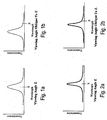
- Figure 1a shows a first filter that has a band pass centered at wavelength X for light that is incident at a given angle Z.
- Figure 2a shows a second filter that has a band pass centered at wavelength X for light that is incident at the same given angle.
- Figure 1b shows a transmission band for the filter shown in Figure 1a at an angle that is oblique to angle Z.
- the transmission band shown in Figure 1b has "shifted" relative to the transmission band shown in Figure 1a , and is now centered at a wavelength that is shorter than wavelength X.
- a transmission band shift of a different magnitude is shown in Figure 2b , which shows the transmission band for the filter of Figure 2a for light incident at an angle that is oblique to angle Z.
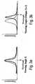
- the present invention combines at least two interference filters, such as those shown in Figures 1a and 2a , to produce a composite filter that undergoes a reduction in total light transmitted as the incident light angle diverges from the given angle.
- Figure 3a shows a light transmission curve for one example of a composite filter of the present invention for light incident at a given angle Z.
- the combination of the two filters results in a filter that transmits light at the given incidence angle in a band that is the union (overlap) of the two transmission bands.
- Figure 3b shows the effect that is achieved for a composite filter of the present invention when light is incident at an angle oblique to Z. As shown in the Figure, the different band shift magnitudes of the two individual filters results in an almost complete transmission blockage over the applicable wavelength range.
- Embodiments of the present invention that use two filters, as just described, can be used to effectively allow viewing at a normal angle through the composite filter while restricting viewing through the filter at oblique angles.
- the "given" angle is the angle that is normal to the surface of the filter, and light transmission will generally decrease as the viewing angle off of the normal viewing angle increases.
- the given angle can be up to 70° off of the normal, which, in various embodiments, results in a filter that allows very little light to pass through at close to the normal angle, but that allows a significant amount of light to pass at angles far off the normal.
- the given angle can be any angle between the normal angle and 60°, 50°, 40°, 30°, or 20° off of the normal.
- filters having multiple peaks in their transmission spectrum can be used as long as at least one peak from each of the two filters exhibit the properties described above and shown in the figures.
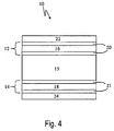
- At least two interference filters are combined to form a composite filter of the present invention, as shown generally at 10 in Figure 4 .
- a first band pass interference filter 12 comprises a first dielectric layer 16 disposed between two reflective layers 20.
- a polymer film 22 is disposed adjacent the first band pass interference filter 12.
- a second band pass interference filter 14 comprises a second dielectric layer 18 disposed between two reflective layers 21.
- a polymer film 24 is disposed adjacent the second band pass filter 14.
- the two polymer films 22, 24 are optional components in these embodiments, and can be added as a substrate onto which the interference filters are formed, or, for example, as an added protective layer.
- the polymer films 22, 24 can include a primer layer to facilitate formation of the interference filter reflective layer component in embodiments in which the polymer films are used as substrates.
- hardcoat layers can be substituted for the polymer films 22, 24, and, in yet further embodiments, rigid substrates such as glass or rigid plastic can be used in place of the polymer films 22, 24. Hardcoat layers can also be used as primer layers or smoothing layers between a band pass interference filter and the substrate on which it is formed.
- a massive spacer 15 which can comprise any suitable material and which will be described in detail below, is disposed between the two interference filters.
- the resulting composite filter 10 will exhibit the combined filtering effect of both of the band pass interference filters as transmitted light is observed across the full range of viewing angles, as described above.
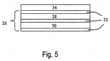
- a dual cavity band pass interference filter 26 comprises a first dielectric layer 28, a second dielectric layer 30, and three reflective layers 32.
- an optional polymer film layer 34 can be included as a substrate upon which to form the filter or as a protective layer.
- Dual cavity filters such as those described above can be used in place of one or both of the single cavity filters shown in Figure 4 in composite filters of the present invention.
- band pass interference filters having three or more dielectric layers and associated reflective layers can also be employed, where appropriate, in place of one or both of the interference filters in a composite filter of the present invention.
- two band pass interference filters are combined with a spacer to form a composite filter of the present invention if the total amount of transmitted visible light at an angle of 45 degrees to the given angle (where the two curve centers are aligned) is less than 80% of the transmitted visible light at the given angle. In some embodiments, the total amount of transmitted visible light at an angle of 45 degrees to the given angle (where the two curve centers are aligned) is less than 60 %, 40%, or 20% of the transmitted visible light at the given angle.
- the figures given immediately above apply to the infrared region of the electromagnetic spectrum, the ultraviolet region, or to other regions, and filters of the present invention can be used in conjunction with infrared remote devices, communication devices, or with any device using any part of the electromagnetic spectrum for which the variable transmission of the present invention would be useful.
- Interference filters of the present invention are useful in a wide variety of light filtering applications, for example, for light collimation, light elimination, or for anti-counterfeiting measures.
- the polymer film shown in Figure 4 as elements 22 and 24 and described herein can be any suitable thermoplastic film that is used in performance film applications.
- the polymer film can comprise polycarbonates, acrylics, nylons, polyesters, polyurethanes, polyolefins such as polypropylene, cellulose acetates and triacetates, vinyl acetals, such as poly(vinyl butyral), vinyl chloride polymers and copolymers and the like, or another plastic suitable for use in a performance film.
- the polymer film is a polyester film, for example poly(ethylene terephthalate).
- the polymer film can have a thickness of 0.012 mm to 0.40 mm, preferably 0.025 mm to 0.1 mm, or 0.04 to 0.06 mm.
- the polymer film can include, where appropriate, a primer layer to facilitate bonding of metalized layers to the polymeric substrate, to provide strength to the substrate, and/or to improve the planarity.
- the polymer films are typically optically transparent (i.e. objects adjacent one side of the layer can be comfortably seen by the eye of a particular observer looking through the layer from the other side).
- the polymer film comprises materials such as re-stretched thermoplastic films having the noted properties, which include polyesters.
- poly(ethylene terephthalate) is used, and, in various embodiments, the poly(ethylene terephthalate) has been biaxially stretched to improve strength, and has been heat stabilized to provide low shrinkage characteristics when subjected to elevated temperatures (e.g. less than 2% shrinkage in both directions after 30 minutes at 150°C).
- a preferred polymer film is poly(ethylene terephthalate).
- a "polymer film” includes multiple layer constructs as well as single layer and coextruded films. For example, two or more separate polymeric layers that are laminated, pressed, or otherwise bound together to form a single film can be used as polymer films of the present invention.
- the thickness of the polymer film can be those given for massive spacers elsewhere herein.
- the dielectric layers of the present invention can comprise any suitable materials, as arc known in the art.
- Useful dielectrics include silicon dioxide, titanium dioxide, magnesium fluoride, and zinc sulfide.
- the following dielectric pairs are used in two single cavity interference filters in a composite filter of the present invention: TiO 2 or Nb 2 O 5 for the first filter, and Si0 2 , MgF 2 , YF 2 for the other filter.
- dielectric pairs having a large difference in index of refraction are preferred. In various embodiments, that difference is one unit or greater.
- the dielectric layers of the present invention can be formed at the appropriate thicknesses so as to provide the desired filtration effect.
- the dielectric layers have a thickness of two or more quarter waves.
- the two layer pair would have a thickness of 340 to 420 nanometers, for example for a MgF 2 layer, and 160 to 240 nanometers, for example for a TiO 2 layer.
- the dielectric layers of the present invention can have any suitable high/low combination of refractive indices, for example, greater than 2 and less than 1.8, and greater than 2.2 and less than 1.5.
- Dielectric layers of the present invention can be formed using any suitable method, as are known in the art, for example, with chemical or physical vapor deposition methods such as evaporation or sputtering.
- Various layer formation techniques are described in Handbook of Thin-Film Deposition Processes and Techniques, edited by Klaus K. Schuegraf. Noyes Publications.
- Reflective layers of the present invention are well known in the art and include any suitable metal composition.
- reflective layers of the present invention comprise a material that is highly reflective to infrared radiation. Examples include silver, gold, aluminum, and copper and their alloys. High infrared radiation reflection is desirable for many applications to prevent the transmission of heat through the filter, such as for embodiments in which incandescent light is filtered. Infrared reflection is also a desirable characteristic for heat sensitive substrates, such as poly(ethylene terephthalate).
- Reflective layers of the present invention can be formed using any suitable method, for example sputtering, and can have any suitable thickness.
- the several reflective layers of the present invention can comprise the same material or different material and can have the same thickness or different thickness, as is desired for a particular embodiment.
- metallic reflective layers comprise silver or silver alloys.
- Massive spacers of the present invention include any suitable laminating adhesives or polymer film layers or combinations of the two. Further, massive spacers can include glass and rigid plastic layers, for example polycarbonate layers, and other suitable rigid substrates.
- Laminating adhesives include those that are conventionally used in the art to bond films together, for example and without limitation, poly(vinyl butyral), polyurethane, silicone, and the like.
- Massive spacers of the present invention include combinations of polymer films and laminating adhesives.
- the two interference filters can be formed on two separate polymer film substrates (elements 22 and 24 in Figure 4 ) and then laminated to a polymer film spacer with an adhesive, in which case the polymer film spacer and the adhesive form the massive spacer.
- Polymer film layers include those disclosed elsewhere herein.
- a massive spacer can be formed using only a polymer film of the desired massive spacer thickness by forming the band pass interference filters directly on a single polymer film.
- a first band pass interference filter is formed on one surface and a second band pass interference filter is formed on the opposite surface of the polymer film.
- the exposed filter surfaces can then be protected with a polymer film layer or a hardcoat, as is known in the art.
- the massive spacer polymer film can include primer layers, as appropriate.
- Massive spacers of the present invention can have any suitable thickness, and in various embodiments the massive spacer has a thickness of at least seven quarter waves optical thickness. In various embodiments, a massive spacer has a thickness of 0.8 to 1.2 micrometers (microns).
- Massive spacers of the present invention can also be combinations of the above-described materials.
- a massive spacer can be a combination of glass and polymer films, wherein one or more polymer films are bonded to the glass.
- Glass and rigid plastic massive spacers of the present invention can have any suitable thickness, and, in various embodiments, such massive spacers can have thicknesses up to 1 millimeter, and, in other embodiments, thicknesses can be greater than 1 millimeter.
- Composite filters of the present invention can effectively be used in many applications, for example and without limitation, as an applied filter on windows and glass applications, as a color filter for various lighting applications, anti-counterfeiting applications, directional light filters, and the like.
- composite interference filters are provided that allow for the variable filtration of light through a range of viewing angles.
- the many benefits of the composite filters is the ability to afford visual privacy through an opening while also allowing the transmission of some of the incident light at acceptable angles.
Landscapes
- Physics & Mathematics (AREA)
- General Physics & Mathematics (AREA)
- Optics & Photonics (AREA)
- Optical Filters (AREA)
Applications Claiming Priority (2)
| Application Number | Priority Date | Filing Date | Title |
|---|---|---|---|
| US12/263,441 US8314991B2 (en) | 2008-10-31 | 2008-10-31 | Variable transmission composite interference filter |
| PCT/US2009/061840 WO2010051231A1 (en) | 2008-10-31 | 2009-10-23 | Variable transmission composite interference filter |
Publications (2)
| Publication Number | Publication Date |
|---|---|
| EP2342591A1 EP2342591A1 (en) | 2011-07-13 |
| EP2342591B1 true EP2342591B1 (en) | 2016-04-13 |
Family
ID=41376297
Family Applications (1)
| Application Number | Title | Priority Date | Filing Date |
|---|---|---|---|
| EP09744281.8A Not-in-force EP2342591B1 (en) | 2008-10-31 | 2009-10-23 | Variable transmission composite interference filter |
Country Status (8)
| Country | Link |
|---|---|
| US (1) | US8314991B2 (zh) |
| EP (1) | EP2342591B1 (zh) |
| JP (1) | JP2012507749A (zh) |
| KR (1) | KR101611641B1 (zh) |
| CN (1) | CN102216817B (zh) |
| BR (1) | BRPI0920529A2 (zh) |
| RU (1) | RU2512089C2 (zh) |
| WO (1) | WO2010051231A1 (zh) |
Families Citing this family (14)
| Publication number | Priority date | Publication date | Assignee | Title |
|---|---|---|---|---|
| JP5682165B2 (ja) * | 2010-07-23 | 2015-03-11 | セイコーエプソン株式会社 | 干渉フィルター、光モジュール、及び分析装置 |
| FR2964458B1 (fr) * | 2010-09-06 | 2012-09-07 | Commissariat Energie Atomique | Dispositif de cartographie et d'analyse a haute resolution d'elements dans des solides |
| DE102013101001B4 (de) * | 2013-01-31 | 2020-10-08 | OSRAM Opto Semiconductors Gesellschaft mit beschränkter Haftung | Optoelektronisches Halbleiterbauteil und Strahlungssensor |
| CN103698829B (zh) * | 2013-11-22 | 2017-03-15 | 中国科学院上海光学精密机械研究所 | 多层介质膜截止滤光片组合器件 |
| KR102197456B1 (ko) | 2014-01-31 | 2020-12-31 | 비아비 솔루션즈 아이엔씨. | 광학 필터 및 분광계 |
| KR102502192B1 (ko) * | 2015-01-23 | 2023-02-21 | 마테리온 코포레이션 | 개선된 투과를 갖는 근적외선 광학 간섭 필터 |
| US10048127B2 (en) | 2015-08-05 | 2018-08-14 | Viavi Solutions Inc. | Optical filter and spectrometer |
| KR20190018550A (ko) * | 2016-07-12 | 2019-02-22 | 쓰리엠 이노베이티브 프로퍼티즈 컴파니 | 광학 스택 |
| KR102306240B1 (ko) * | 2017-04-17 | 2021-09-30 | 가부시키가이샤 무라타 세이사쿠쇼 | 탄성파 장치, 고주파 프론트 엔드 회로 및 통신 장치 |
| DE102017126832B4 (de) * | 2017-11-15 | 2021-07-29 | Hensoldt Optronics Gmbh | Laservorrichtung |
| US20190162885A1 (en) * | 2017-11-30 | 2019-05-30 | Qualcomm Incorporated | Optical bandpass filter design |
| US11215741B2 (en) * | 2018-01-17 | 2022-01-04 | Viavi Solutions Inc. | Angle of incidence restriction for optical filters |
| CN110824599B (zh) * | 2018-08-14 | 2021-09-03 | 白金科技股份有限公司 | 一种红外带通滤波器 |
| RU203242U1 (ru) * | 2020-12-04 | 2021-03-29 | Федеральное государственное учреждение "Федеральный научно-исследовательский центр "Кристаллография и фотоника" Российской академии наук" | Составной интерференционный фильтр |
Family Cites Families (24)
| Publication number | Priority date | Publication date | Assignee | Title |
|---|---|---|---|---|
| DE3300849A1 (de) | 1983-01-13 | 1984-07-19 | Standard Elektrik Lorenz Ag, 7000 Stuttgart | Vorrichtung zum ermitteln der einfallsrichtung von optischer strahlung |
| SU1748112A1 (ru) * | 1990-05-11 | 1992-07-15 | Харьковский государственный университет им.А.М.Горького | Интерференционный фильтр |
| US5159199A (en) | 1991-08-12 | 1992-10-27 | The United States Of America As Represented By The Administrator Of The National Aeronautics And Space Administration | Integrated filter and detector array for spectral imaging |
| JP3166115B2 (ja) * | 1993-08-03 | 2001-05-14 | 富士写真フイルム株式会社 | フィルタ装置 |
| US5502595A (en) | 1994-06-03 | 1996-03-26 | Industrial Technology Research Institute | Color filters and their preparation |
| JPH08237203A (ja) | 1995-02-23 | 1996-09-13 | Fujitsu Ltd | 光フィルタアレイ、光送信機及び光送信システム |
| US6031653A (en) * | 1997-08-28 | 2000-02-29 | California Institute Of Technology | Low-cost thin-metal-film interference filters |
| US6112005A (en) * | 1997-11-12 | 2000-08-29 | Alliance Fiber Optics Products, Inc. | Filter device for use with light and method making the same |
| US6569515B2 (en) | 1998-01-13 | 2003-05-27 | 3M Innovative Properties Company | Multilayered polymer films with recyclable or recycled layers |
| US6049419A (en) | 1998-01-13 | 2000-04-11 | 3M Innovative Properties Co | Multilayer infrared reflecting optical body |
| US6808658B2 (en) | 1998-01-13 | 2004-10-26 | 3M Innovative Properties Company | Method for making texture multilayer optical films |
| JPH11307987A (ja) * | 1998-04-16 | 1999-11-05 | Nippon Sheet Glass Co Ltd | 電磁波フィルタ |
| AU2005202375A1 (en) * | 1999-08-20 | 2005-06-23 | Cpfilms, Inc. | Optical filter for a window |
| US7002696B1 (en) | 2000-11-03 | 2006-02-21 | Optune Technologies | Band pass interferometer with tuning capabilities |
| US6717965B2 (en) | 2001-07-06 | 2004-04-06 | Intel Corporation | Graded thin film wedge interference filter and method of use for laser tuning |
| US6865315B2 (en) | 2001-08-29 | 2005-03-08 | Jds Uniphase Corporation | Dispersion compensating filters |
| US6804063B2 (en) | 2002-10-25 | 2004-10-12 | Research Electro-Optics, Inc. | Optical interference filter having parallel phase control elements |
| JP2005003806A (ja) | 2003-06-10 | 2005-01-06 | Sun Tec Kk | 光学素子、波長可変光フィルタおよび光アドドロップモジュール |
| JP4401880B2 (ja) * | 2004-07-09 | 2010-01-20 | 光伸光学工業株式会社 | 多重バンドパスフィルタ |
| US7289197B2 (en) | 2004-12-22 | 2007-10-30 | Anthony Stephen Kewitsch | Transmissive optical detector |
| CA2537732A1 (en) * | 2005-04-06 | 2006-10-06 | Jds Uniphase Corporation | High chroma optically variable colour-shifting glitter |
| US20060256428A1 (en) | 2005-05-16 | 2006-11-16 | Lake Shore Cryotronics, Inc. | Long wave pass infrared filter based on porous semiconductor material and the method of manufacturing the same |
| US7848000B2 (en) | 2006-01-09 | 2010-12-07 | Chemimage Corporation | Birefringent spectral filter with wide field of view and associated communications method and apparatus |
| US7317576B2 (en) * | 2006-04-21 | 2008-01-08 | Cpfilms, Inc. | Dichroic filters on flexible polymer film substrates |
-
2008
- 2008-10-31 US US12/263,441 patent/US8314991B2/en not_active Expired - Fee Related
-
2009
- 2009-10-23 CN CN2009801439013A patent/CN102216817B/zh not_active Expired - Fee Related
- 2009-10-23 RU RU2011121822/28A patent/RU2512089C2/ru not_active IP Right Cessation
- 2009-10-23 KR KR1020117009740A patent/KR101611641B1/ko active IP Right Grant
- 2009-10-23 EP EP09744281.8A patent/EP2342591B1/en not_active Not-in-force
- 2009-10-23 BR BRPI0920529A patent/BRPI0920529A2/pt not_active Application Discontinuation
- 2009-10-23 JP JP2011534645A patent/JP2012507749A/ja active Pending
- 2009-10-23 WO PCT/US2009/061840 patent/WO2010051231A1/en active Application Filing
Also Published As
| Publication number | Publication date |
|---|---|
| BRPI0920529A2 (pt) | 2015-12-29 |
| KR20110086552A (ko) | 2011-07-28 |
| RU2512089C2 (ru) | 2014-04-10 |
| JP2012507749A (ja) | 2012-03-29 |
| US20100110550A1 (en) | 2010-05-06 |
| KR101611641B1 (ko) | 2016-04-11 |
| CN102216817B (zh) | 2013-09-25 |
| EP2342591A1 (en) | 2011-07-13 |
| CN102216817A (zh) | 2011-10-12 |
| RU2011121822A (ru) | 2012-12-10 |
| US8314991B2 (en) | 2012-11-20 |
| WO2010051231A1 (en) | 2010-05-06 |
Similar Documents
| Publication | Publication Date | Title |
|---|---|---|
| EP2342591B1 (en) | Variable transmission composite interference filter | |
| US11585962B2 (en) | Transparent covering having anti-reflective coatings | |
| KR100691544B1 (ko) | 반사 방지 중합체 구조물 및 이것의 제조 방법 | |
| US6650478B1 (en) | Optical filter for a window | |
| CA1335086C (en) | Multilayer heat-reflecting composite films and glazing products containing the same | |
| JP4314357B2 (ja) | 透明多層デバイス | |
| EP2030051B1 (en) | Multiple band reflector with metal and dielectric layers | |
| US20120099188A1 (en) | Laser Protection Structures and Methods of Fabrication | |
| JP2004526995A (ja) | 複数層薄膜光学的フィルタ構成体 | |
| KR20170030066A (ko) | 투명 차열 단열 부재 및 그 제조 방법 | |
| CN112444898B (zh) | 一种宽角度应用的滤光片 | |
| CA2856776A1 (en) | Laminated glass for use in vehicles or in architecture | |
| US7317576B2 (en) | Dichroic filters on flexible polymer film substrates | |
| AU2005202375A1 (en) | Optical filter for a window | |
| WO2021116849A1 (en) | Optical filter and optical system | |
| US20230003928A1 (en) | Flexible, ultra-thin, hybrid absorptive-reflective thin-film filters and methods of making the same | |
| AU2008207561A1 (en) | Optical filter for a window |
Legal Events
| Date | Code | Title | Description |
|---|---|---|---|
| PUAI | Public reference made under article 153(3) epc to a published international application that has entered the european phase |
Free format text: ORIGINAL CODE: 0009012 |
|
| 17P | Request for examination filed |
Effective date: 20110420 |
|
| AK | Designated contracting states |
Kind code of ref document: A1 Designated state(s): AT BE BG CH CY CZ DE DK EE ES FI FR GB GR HR HU IE IS IT LI LT LU LV MC MK MT NL NO PL PT RO SE SI SK SM TR |
|
| AX | Request for extension of the european patent |
Extension state: AL BA RS |
|
| DAX | Request for extension of the european patent (deleted) | ||
| GRAP | Despatch of communication of intention to grant a patent |
Free format text: ORIGINAL CODE: EPIDOSNIGR1 |
|
| INTG | Intention to grant announced |
Effective date: 20151027 |
|
| GRAS | Grant fee paid |
Free format text: ORIGINAL CODE: EPIDOSNIGR3 |
|
| GRAA | (expected) grant |
Free format text: ORIGINAL CODE: 0009210 |
|
| AK | Designated contracting states |
Kind code of ref document: B1 Designated state(s): AT BE BG CH CY CZ DE DK EE ES FI FR GB GR HR HU IE IS IT LI LT LU LV MC MK MT NL NO PL PT RO SE SI SK SM TR |
|
| REG | Reference to a national code |
Ref country code: GB Ref legal event code: FG4D |
|
| REG | Reference to a national code |
Ref country code: AT Ref legal event code: REF Ref document number: 790737 Country of ref document: AT Kind code of ref document: T Effective date: 20160415 Ref country code: CH Ref legal event code: EP |
|
| REG | Reference to a national code |
Ref country code: IE Ref legal event code: FG4D |
|
| REG | Reference to a national code |
Ref country code: DE Ref legal event code: R096 Ref document number: 602009037780 Country of ref document: DE |
|
| REG | Reference to a national code |
Ref country code: LT Ref legal event code: MG4D |
|
| REG | Reference to a national code |
Ref country code: AT Ref legal event code: MK05 Ref document number: 790737 Country of ref document: AT Kind code of ref document: T Effective date: 20160413 |
|
| REG | Reference to a national code |
Ref country code: NL Ref legal event code: MP Effective date: 20160413 |
|
| REG | Reference to a national code |
Ref country code: FR Ref legal event code: PLFP Year of fee payment: 8 |
|
| PG25 | Lapsed in a contracting state [announced via postgrant information from national office to epo] |
Ref country code: PL Free format text: LAPSE BECAUSE OF FAILURE TO SUBMIT A TRANSLATION OF THE DESCRIPTION OR TO PAY THE FEE WITHIN THE PRESCRIBED TIME-LIMIT Effective date: 20160413 Ref country code: NO Free format text: LAPSE BECAUSE OF FAILURE TO SUBMIT A TRANSLATION OF THE DESCRIPTION OR TO PAY THE FEE WITHIN THE PRESCRIBED TIME-LIMIT Effective date: 20160713 Ref country code: LT Free format text: LAPSE BECAUSE OF FAILURE TO SUBMIT A TRANSLATION OF THE DESCRIPTION OR TO PAY THE FEE WITHIN THE PRESCRIBED TIME-LIMIT Effective date: 20160413 Ref country code: FI Free format text: LAPSE BECAUSE OF FAILURE TO SUBMIT A TRANSLATION OF THE DESCRIPTION OR TO PAY THE FEE WITHIN THE PRESCRIBED TIME-LIMIT Effective date: 20160413 Ref country code: NL Free format text: LAPSE BECAUSE OF FAILURE TO SUBMIT A TRANSLATION OF THE DESCRIPTION OR TO PAY THE FEE WITHIN THE PRESCRIBED TIME-LIMIT Effective date: 20160413 |
|
| PG25 | Lapsed in a contracting state [announced via postgrant information from national office to epo] |
Ref country code: SE Free format text: LAPSE BECAUSE OF FAILURE TO SUBMIT A TRANSLATION OF THE DESCRIPTION OR TO PAY THE FEE WITHIN THE PRESCRIBED TIME-LIMIT Effective date: 20160413 Ref country code: LV Free format text: LAPSE BECAUSE OF FAILURE TO SUBMIT A TRANSLATION OF THE DESCRIPTION OR TO PAY THE FEE WITHIN THE PRESCRIBED TIME-LIMIT Effective date: 20160413 Ref country code: PT Free format text: LAPSE BECAUSE OF FAILURE TO SUBMIT A TRANSLATION OF THE DESCRIPTION OR TO PAY THE FEE WITHIN THE PRESCRIBED TIME-LIMIT Effective date: 20160816 Ref country code: GR Free format text: LAPSE BECAUSE OF FAILURE TO SUBMIT A TRANSLATION OF THE DESCRIPTION OR TO PAY THE FEE WITHIN THE PRESCRIBED TIME-LIMIT Effective date: 20160714 Ref country code: AT Free format text: LAPSE BECAUSE OF FAILURE TO SUBMIT A TRANSLATION OF THE DESCRIPTION OR TO PAY THE FEE WITHIN THE PRESCRIBED TIME-LIMIT Effective date: 20160413 Ref country code: HR Free format text: LAPSE BECAUSE OF FAILURE TO SUBMIT A TRANSLATION OF THE DESCRIPTION OR TO PAY THE FEE WITHIN THE PRESCRIBED TIME-LIMIT Effective date: 20160413 Ref country code: ES Free format text: LAPSE BECAUSE OF FAILURE TO SUBMIT A TRANSLATION OF THE DESCRIPTION OR TO PAY THE FEE WITHIN THE PRESCRIBED TIME-LIMIT Effective date: 20160413 |
|
| PG25 | Lapsed in a contracting state [announced via postgrant information from national office to epo] |
Ref country code: IT Free format text: LAPSE BECAUSE OF FAILURE TO SUBMIT A TRANSLATION OF THE DESCRIPTION OR TO PAY THE FEE WITHIN THE PRESCRIBED TIME-LIMIT Effective date: 20160413 Ref country code: BE Free format text: LAPSE BECAUSE OF FAILURE TO SUBMIT A TRANSLATION OF THE DESCRIPTION OR TO PAY THE FEE WITHIN THE PRESCRIBED TIME-LIMIT Effective date: 20160413 |
|
| REG | Reference to a national code |
Ref country code: DE Ref legal event code: R097 Ref document number: 602009037780 Country of ref document: DE |
|
| PG25 | Lapsed in a contracting state [announced via postgrant information from national office to epo] |
Ref country code: SK Free format text: LAPSE BECAUSE OF FAILURE TO SUBMIT A TRANSLATION OF THE DESCRIPTION OR TO PAY THE FEE WITHIN THE PRESCRIBED TIME-LIMIT Effective date: 20160413 Ref country code: CZ Free format text: LAPSE BECAUSE OF FAILURE TO SUBMIT A TRANSLATION OF THE DESCRIPTION OR TO PAY THE FEE WITHIN THE PRESCRIBED TIME-LIMIT Effective date: 20160413 Ref country code: DK Free format text: LAPSE BECAUSE OF FAILURE TO SUBMIT A TRANSLATION OF THE DESCRIPTION OR TO PAY THE FEE WITHIN THE PRESCRIBED TIME-LIMIT Effective date: 20160413 Ref country code: RO Free format text: LAPSE BECAUSE OF FAILURE TO SUBMIT A TRANSLATION OF THE DESCRIPTION OR TO PAY THE FEE WITHIN THE PRESCRIBED TIME-LIMIT Effective date: 20160413 Ref country code: EE Free format text: LAPSE BECAUSE OF FAILURE TO SUBMIT A TRANSLATION OF THE DESCRIPTION OR TO PAY THE FEE WITHIN THE PRESCRIBED TIME-LIMIT Effective date: 20160413 |
|
| PLBE | No opposition filed within time limit |
Free format text: ORIGINAL CODE: 0009261 |
|
| STAA | Information on the status of an ep patent application or granted ep patent |
Free format text: STATUS: NO OPPOSITION FILED WITHIN TIME LIMIT |
|
| PG25 | Lapsed in a contracting state [announced via postgrant information from national office to epo] |
Ref country code: SM Free format text: LAPSE BECAUSE OF FAILURE TO SUBMIT A TRANSLATION OF THE DESCRIPTION OR TO PAY THE FEE WITHIN THE PRESCRIBED TIME-LIMIT Effective date: 20160413 |
|
| 26N | No opposition filed |
Effective date: 20170116 |
|
| PG25 | Lapsed in a contracting state [announced via postgrant information from national office to epo] |
Ref country code: SI Free format text: LAPSE BECAUSE OF FAILURE TO SUBMIT A TRANSLATION OF THE DESCRIPTION OR TO PAY THE FEE WITHIN THE PRESCRIBED TIME-LIMIT Effective date: 20160413 |
|
| REG | Reference to a national code |
Ref country code: CH Ref legal event code: PL |
|
| GBPC | Gb: european patent ceased through non-payment of renewal fee |
Effective date: 20161023 |
|
| REG | Reference to a national code |
Ref country code: IE Ref legal event code: MM4A |
|
| PG25 | Lapsed in a contracting state [announced via postgrant information from national office to epo] |
Ref country code: GB Free format text: LAPSE BECAUSE OF NON-PAYMENT OF DUE FEES Effective date: 20161023 Ref country code: CH Free format text: LAPSE BECAUSE OF NON-PAYMENT OF DUE FEES Effective date: 20161031 Ref country code: LI Free format text: LAPSE BECAUSE OF NON-PAYMENT OF DUE FEES Effective date: 20161031 |
|
| PG25 | Lapsed in a contracting state [announced via postgrant information from national office to epo] |
Ref country code: LU Free format text: LAPSE BECAUSE OF NON-PAYMENT OF DUE FEES Effective date: 20161023 |
|
| REG | Reference to a national code |
Ref country code: FR Ref legal event code: PLFP Year of fee payment: 9 |
|
| PG25 | Lapsed in a contracting state [announced via postgrant information from national office to epo] |
Ref country code: IE Free format text: LAPSE BECAUSE OF NON-PAYMENT OF DUE FEES Effective date: 20161023 |
|
| PG25 | Lapsed in a contracting state [announced via postgrant information from national office to epo] |
Ref country code: CY Free format text: LAPSE BECAUSE OF FAILURE TO SUBMIT A TRANSLATION OF THE DESCRIPTION OR TO PAY THE FEE WITHIN THE PRESCRIBED TIME-LIMIT Effective date: 20160413 Ref country code: HU Free format text: LAPSE BECAUSE OF FAILURE TO SUBMIT A TRANSLATION OF THE DESCRIPTION OR TO PAY THE FEE WITHIN THE PRESCRIBED TIME-LIMIT; INVALID AB INITIO Effective date: 20091023 |
|
| PG25 | Lapsed in a contracting state [announced via postgrant information from national office to epo] |
Ref country code: TR Free format text: LAPSE BECAUSE OF FAILURE TO SUBMIT A TRANSLATION OF THE DESCRIPTION OR TO PAY THE FEE WITHIN THE PRESCRIBED TIME-LIMIT Effective date: 20160413 Ref country code: MT Free format text: LAPSE BECAUSE OF NON-PAYMENT OF DUE FEES Effective date: 20161031 Ref country code: IS Free format text: LAPSE BECAUSE OF FAILURE TO SUBMIT A TRANSLATION OF THE DESCRIPTION OR TO PAY THE FEE WITHIN THE PRESCRIBED TIME-LIMIT Effective date: 20160413 Ref country code: MK Free format text: LAPSE BECAUSE OF FAILURE TO SUBMIT A TRANSLATION OF THE DESCRIPTION OR TO PAY THE FEE WITHIN THE PRESCRIBED TIME-LIMIT Effective date: 20160413 Ref country code: MC Free format text: LAPSE BECAUSE OF FAILURE TO SUBMIT A TRANSLATION OF THE DESCRIPTION OR TO PAY THE FEE WITHIN THE PRESCRIBED TIME-LIMIT Effective date: 20160413 |
|
| PG25 | Lapsed in a contracting state [announced via postgrant information from national office to epo] |
Ref country code: BG Free format text: LAPSE BECAUSE OF FAILURE TO SUBMIT A TRANSLATION OF THE DESCRIPTION OR TO PAY THE FEE WITHIN THE PRESCRIBED TIME-LIMIT Effective date: 20160413 |
|
| REG | Reference to a national code |
Ref country code: FR Ref legal event code: PLFP Year of fee payment: 10 |
|
| REG | Reference to a national code |
Ref country code: DE Ref legal event code: R082 Ref document number: 602009037780 Country of ref document: DE Representative=s name: WALLINGER RICKER SCHLOTTER TOSTMANN PATENT- UN, DE Ref country code: DE Ref legal event code: R081 Ref document number: 602009037780 Country of ref document: DE Owner name: EASTMAN PERFORMANCE FILMS, LLC, ST. LOUIS, US Free format text: FORMER OWNER: CPFILMS INC., FIELDALE, VA., US |
|
| REG | Reference to a national code |
Ref country code: FR Ref legal event code: CA Effective date: 20181022 Ref country code: FR Ref legal event code: CD Owner name: EASTMAN PERFORMANCE FILMS, LLC, US Effective date: 20181022 Ref country code: FR Ref legal event code: CJ Effective date: 20181022 |
|
| PGFP | Annual fee paid to national office [announced via postgrant information from national office to epo] |
Ref country code: FR Payment date: 20190924 Year of fee payment: 11 |
|
| PGFP | Annual fee paid to national office [announced via postgrant information from national office to epo] |
Ref country code: DE Payment date: 20190917 Year of fee payment: 11 |
|
| REG | Reference to a national code |
Ref country code: DE Ref legal event code: R119 Ref document number: 602009037780 Country of ref document: DE |
|
| PG25 | Lapsed in a contracting state [announced via postgrant information from national office to epo] |
Ref country code: DE Free format text: LAPSE BECAUSE OF NON-PAYMENT OF DUE FEES Effective date: 20210501 Ref country code: FR Free format text: LAPSE BECAUSE OF NON-PAYMENT OF DUE FEES Effective date: 20201031 |